EP1154391A1 - Etiquette d'adhesion - Google Patents
Etiquette d'adhesion Download PDFInfo
- Publication number
- EP1154391A1 EP1154391A1 EP00956795A EP00956795A EP1154391A1 EP 1154391 A1 EP1154391 A1 EP 1154391A1 EP 00956795 A EP00956795 A EP 00956795A EP 00956795 A EP00956795 A EP 00956795A EP 1154391 A1 EP1154391 A1 EP 1154391A1
- Authority
- EP
- European Patent Office
- Prior art keywords
- adhesive
- circuit substrate
- data carrier
- electronic components
- adhesive label
- Prior art date
- Legal status (The legal status is an assumption and is not a legal conclusion. Google has not performed a legal analysis and makes no representation as to the accuracy of the status listed.)
- Granted
Links
Images
Classifications
-
- G—PHYSICS
- G06—COMPUTING; CALCULATING OR COUNTING
- G06K—GRAPHICAL DATA READING; PRESENTATION OF DATA; RECORD CARRIERS; HANDLING RECORD CARRIERS
- G06K19/00—Record carriers for use with machines and with at least a part designed to carry digital markings
- G06K19/06—Record carriers for use with machines and with at least a part designed to carry digital markings characterised by the kind of the digital marking, e.g. shape, nature, code
-
- G—PHYSICS
- G06—COMPUTING; CALCULATING OR COUNTING
- G06K—GRAPHICAL DATA READING; PRESENTATION OF DATA; RECORD CARRIERS; HANDLING RECORD CARRIERS
- G06K19/00—Record carriers for use with machines and with at least a part designed to carry digital markings
- G06K19/02—Record carriers for use with machines and with at least a part designed to carry digital markings characterised by the selection of materials, e.g. to avoid wear during transport through the machine
- G06K19/027—Record carriers for use with machines and with at least a part designed to carry digital markings characterised by the selection of materials, e.g. to avoid wear during transport through the machine the material being suitable for use as a textile, e.g. woven-based RFID-like labels designed for attachment to laundry items
-
- G—PHYSICS
- G06—COMPUTING; CALCULATING OR COUNTING
- G06K—GRAPHICAL DATA READING; PRESENTATION OF DATA; RECORD CARRIERS; HANDLING RECORD CARRIERS
- G06K19/00—Record carriers for use with machines and with at least a part designed to carry digital markings
- G06K19/06—Record carriers for use with machines and with at least a part designed to carry digital markings characterised by the kind of the digital marking, e.g. shape, nature, code
- G06K19/067—Record carriers with conductive marks, printed circuits or semiconductor circuit elements, e.g. credit or identity cards also with resonating or responding marks without active components
- G06K19/07—Record carriers with conductive marks, printed circuits or semiconductor circuit elements, e.g. credit or identity cards also with resonating or responding marks without active components with integrated circuit chips
- G06K19/077—Constructional details, e.g. mounting of circuits in the carrier
- G06K19/07749—Constructional details, e.g. mounting of circuits in the carrier the record carrier being capable of non-contact communication, e.g. constructional details of the antenna of a non-contact smart card
- G06K19/07758—Constructional details, e.g. mounting of circuits in the carrier the record carrier being capable of non-contact communication, e.g. constructional details of the antenna of a non-contact smart card arrangements for adhering the record carrier to further objects or living beings, functioning as an identification tag
- G06K19/0776—Constructional details, e.g. mounting of circuits in the carrier the record carrier being capable of non-contact communication, e.g. constructional details of the antenna of a non-contact smart card arrangements for adhering the record carrier to further objects or living beings, functioning as an identification tag the adhering arrangement being a layer of adhesive, so that the record carrier can function as a sticker
-
- G—PHYSICS
- G09—EDUCATION; CRYPTOGRAPHY; DISPLAY; ADVERTISING; SEALS
- G09F—DISPLAYING; ADVERTISING; SIGNS; LABELS OR NAME-PLATES; SEALS
- G09F3/00—Labels, tag tickets, or similar identification or indication means; Seals; Postage or like stamps
- G09F3/02—Forms or constructions
-
- G—PHYSICS
- G09—EDUCATION; CRYPTOGRAPHY; DISPLAY; ADVERTISING; SEALS
- G09F—DISPLAYING; ADVERTISING; SIGNS; LABELS OR NAME-PLATES; SEALS
- G09F3/00—Labels, tag tickets, or similar identification or indication means; Seals; Postage or like stamps
- G09F3/08—Fastening or securing by means not forming part of the material of the label itself
- G09F3/10—Fastening or securing by means not forming part of the material of the label itself by an adhesive layer
Definitions
- the present invention relates to an adhesive label, more particularly to a contactless data carrier adhesive label.
- the present invention may be advantageously applied to a contactless data carrier or a radio frequency identification card in the form of an adhesive label.
- a contactless data carrier system includes a data carrier (a transponder) and an interrogator, and a data transmission is made without contact therebetween.
- the contactless data carrier system in the form of an adhesive label, is applied, for example, to management of articles to be distributed, by sticking an adhesive label-type data carrier or transponder on a surface of an article, such as personal baggage, to be distributed, or the management of FA (Factory Automation) by sticking an adhesive label-type data carrier or transponder on a surface of a machine component in an assembly-line operation.
- FA Vectory Automation
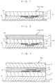
- a typical conventionally used adhesive label-type data carrier has a structure such that a contactless data carrier element mounted on a surface of a circuit substrate 1 is sealed with a resin layer 3, and a surface layer 4 is laminated on the resin layer 3.
- the contactless data carrier element contains, for example, an electric circuit 21 and electronic components 2 such as an IC chip, a capacitor, a battery and so on.
- an entire contactless data carrier element is formed on one side of the circuit substrate 1, as shown in Fig. 3.
- the contactless data carrier element may be prepared by separately forming a part of an electric circuit on each side of the circuit substrate 1, and connecting one to the other via a through-hole, to thus integrate the separately formed parts into a sole contactless data carrier element.
- an adhesive layer 5 is provided on a reverse side of the circuit substrate 1 of the adhesive label-type data carrier.
- the adhesive label-type data carrier is temporarily applied on a release sheet (not shown).
- the adhesive label-type data carrier is peeled therefrom, and applied to a surface of an article 6.
- a mark for identification and so on is generally printed on a label surface 4a, i.e., a surface 4a of the surface layer 4.
- the electronic components forming the contactless data carrier element are thicker than the electric circuit, and thus, an irregular or uneven structure is formed on one surface of the circuit substrate 1. Therefore, this poses a disadvantageous problem in that the irregular or uneven structure affects the surface 4a of the surface layer 4, and a mottle of printing, such as a pin hole occurs.
- the object of the present invention is to provide an adhesive label-type contactless data carrier wherein the irregular or uneven structure formed due to the presence of electronic components on a flat circuit substrate of the contactless data carrier element is not reflected on the label surface; a thinning of the structure can be realized; and an excellent printability obtained.
- an adhesive label according to the present invention characterized by comprising a circuit substrate, electronic components formed on one surface of the circuit substrate, and an adhesive layer on the electronic components to be applied to an article, which are sequentially laminated.
- the adhesive layer is a pressure sensitive adhesive layer.
- a surface layer is provided on a circuit substrate surface that is a reverse side to a surface carrying the electronic components.
- Fig. 1 is a sectional view schematically illustrating a state wherein an adhesive label 10 as an embodiment of the present invention is applied to a surface of an article 6.
- One of main purposes of the sectional views including Fig. 1 attached to the present specification is to illustrate structures of the adhesive label. Therefore, the thickness of each layer illustrated is exaggerated, and the ratios of the layers are not precise.
- the adhesive label 10 of the present invention is composed of the circuit substrate 1; the contactless data carrier element containing an electric circuit 21 and an IC chip 2, and formed on one surface 1a; and the adhesive layer 7 covering and containing the contactless data carrier element.
- the adhesive label 10 is stuck to and held on a surface of an article 6 by the adhesive layer 7, and thus the other surface 1b of the circuit substrate 1 becomes a label surface 10b.
- the label surface 10b of the adhesive label 10 of the present invention is sufficiently flat that, when stuck on a release sheet (not shown) or the article 6 via the adhesive layer 7, it can be printed without any mottle of printing.
- the adhesive label 10 of the present invention as shown in Fig. 1 can be made thinner in comparison with the conventional adhesive label-type data carrier.
- the conventional adhesive label-type data carrier as shown in Fig. 3 has a 4-layered structure composed of the surface layer 4, the resin layer 3 covering and sealing the contactless data carrier element containing the electric circuit 21 and IC chip 2, the circuit substrate 1, and the pressure sensitive adhesive layer 5.
- the adhesive label 10 of the present invention as shown in Fig. 1 has a 2-layered structure composed of the circuit substrate 1, and the adhesive layer 7 covering and containing the contactless data carrier element containing the electric circuit 21 and IC chip 2. Therefore, a thickness of the adhesive label 10 of the present invention can be thinned as a whole, the number of the materials used can be reduced, the manufacturing process can be simplified, and the manufacturing cost can be reduced.
- a surface layer can be added onto the circuit substrate 1, when the circuit substrate 1 of the adhesive label 10 of the present invention as shown in Fig. 1 is transparent or translucent, and thus the contactless data carrier element can be unfavorably seen through the circuit substrate 1 from the label surface 10b, when the material of the circuit substrate 1 has an insufficient printability, or when a part of the electric circuit is formed on a reverse surface to the surface carrying the electronic components such as the IC chip 2.
- the surface layer can provide a concealing effect or printability.
- Fig. 2 is a sectional view schematically illustrating a state where the adhesive label 10 as the embodiment of the present invention having the surface layer is stuck on a surface of the article 6.
- the adhesive label 10 as shown in Fig. 2 comprises the circuit substrate 1, the contactless data carrier element containing the electric circuit 21 and IC chip 2 and formed on one surface 1a of the circuit substrate 1, the adhesive layer 7 covering and containing the contactless data carrier element, and the surface layer 4 formed on another surface of the circuit substrate 1.
- the surface 4b that does not come into contact with the circuit substrate 1 becomes the label surface 10b of the adhesive label 10.
- the label surface 10b of the adhesive label 10 of the present invention is sufficiently flat when stuck on a release sheet (not shown) or the article 6 via the adhesive layer 7, and therefore, can be printed without any mottle of printing. Further, a concealing effect can be obtained when an opaque material is used as the surface layer 4.
- a part of the electric circuit may be formed on each surface of the circuit substrate 1 and connected one to the other via a through-hole, to thus integrate the separately formed parts in to a contactless data carrier element. It is preferable to form a thinner electric circuit on the side of the surface layer.
- a thin electric circuit can be formed, for example, by printing the surface with a silver paste, or sputtering.
- the circuit substrate which may be used in the present invention is not particularly limited, so long as it will function as a support capable of stably carrying an entire contactless data carrier element or at least a part of the electronic components and the electric circuit of an entire contactless data carrier element on one surface, and maintaining a flatness, and at the same time stably carrying a part of the thin electric circuit on the other surface.
- the circuit substrate may be transparent, translucent, or opaque.
- the circuit substrate may be, for example, a paper, a sheet of a natural or synthetic fibrous material, such as a woven fabric sheet, a knitted fabric sheet or a non-woven fabric sheet, a synthetic resin film or sheet.
- synthetic resin there may be mentioned, for example, polyethylene, polypropylene, polyvinyl chloride, polystyrene, polyester such as polyethylene terephthalate or polyethylene naphthalate, polybutene, polyacrylate, polymethacrylate, polyvinyl alcohol, polyvinyl butyral, polyimide, polycarbonate, polyamide, ethylene-vinyl acetate copolymer, ethylene acrylate copolymer, polyvinyl acetal, ethyl cellulose, cellulose triacetate, hydroxypropyl cellulose, or acrylonitrile-butadiene-stylene copolymer, or the like.
- the circuit substrate is preferably opaque.
- the opaque substrate film used may be a substrate made of an opaque material, such as the above-mentioned paper or fibrous material, or a substrate prepared by opacifying the above-mentioned transparent resin film in accordance with any known conventional opacifying methods.
- the conventional opacifying methods may be, for example, a method wherein an opacifying agent, such as titanium oxide or calcium carbonate is incorporated to the film, a method wherein the film surface is coated or printed with the opacifying agent together with a binder, a method wherein a foaming agent is used, or a method wherein talc having a poor compatibility with the film or the like is incorporated to the film, and then the film is expanded to form micropores in the film, or the like.
- an opacifying agent such as titanium oxide or calcium carbonate
- the thickness of the circuit substrate is not particularly limited, but is preferably 25 ⁇ m to 200 ⁇ m.
- the contactless data carrier element formed on the surface of the circuit substrate may be composed of the electronic components and the electric circuit.
- the electric circuit comprises lead wires and antenna coils.
- the electronic components include, for example, an IC chip, a battery, a capacitor, a resistor, a coil, a diode, or the like.
- the contactless data carrier element may be formed on one or both surfaces of the circuit substrate according to any known methods. For example, an IC chip, a battery, or a capacitor may be fixed or connected with an adhesive, a solder or an electrically conductive resin to form the contactless data carrier element.
- the electric circuit may be formed on one surface of the circuit substrate by printing the surface with an electrically conductive resin, sputtering a metal, or etching a metal foil that has been applied on a surface of the circuit substrate.
- the adhesive layer coating the contactless data carrier element may be formed from any pressure sensitive adhesive or heat sensitive adhesive.
- the pressure sensitive adhesive used in the adhesive layer there may be mentioned, for example, an adhesive based on natural rubber, synthetic rubber, acrylic resin, polyvinyl ether resin, urethane resin, or silicone resin.
- the synthetic rubber-based adhesive may be, for example, styrene-butadiene rubber, polyisobutylene rubber, isobutylene-isoprene rubber, isoprene rubber, styreneisoprene block copolymer, styrene-butadiene block copolymer, styrene-ethylene-butylene block copolymer, or the like.
- the acrylic resin-based adhesive may be, for example, a homopolymer or copolymer of acrylic acid, methyl acrylate, ethyl acrylate, propyl acrylate, butyl acrylate, 2-ethylhexyl acrylate, ethyl methacrylate, butyl methacrylate, acrylonitrile or the like.
- the polyvinyl ether resin-based adhesive may be, for example, polyvinyl ether, polyvinyl isobutyl ether or the like.
- the silicone resin-based adhesive may be, for example, dimethyl polysiloxane.
- the heat sensitive adhesive used in the adhesive layer there may be mentioned, for example, an adhesive based on polyethylene, ethylene-vinyl acetate resin, polyester resin, or polyimide resin.
- the pressure sensitive adhesive is preferably used, because of the ease with which it can be stuck to an article.
- the adhesive layer can be formed by coating the circuit substrate carrying the contactless data carrier element with the pressure sensitive adhesives or heat sensitive adhesives according to known methods, for example, by means of a roll coater, a knife coater, a die coater/blade coater, a gravure coater, a screen printing, or the like.
- the thickness of the adhesive layer is generally 20 to 150 ⁇ m.
- the adhesive layer may be a double-coated adhesive layer having an adhesive layer on each surface of a support sheet.
- the support sheet may be a material the same as those mentioned for the circuit substrate.
- the thickness of the support sheet is not particularly limited, but is generally 5 to 30 ⁇ m.
- the adhesive layers formed on both surfaces of the support sheet have a thickness of, preferably 20 to 150 ⁇ m, on the circuit substrate side, and a thickness of, preferably 20 to 100 ⁇ m, on the article side.
- the release sheet is not particularly limited, but for example, is a film of polyethylene terephthalate, polybutylene terephthalate, polyethylene, or polypropylene, polyarylate, or the like, a paper, such as polyethylene laminated paper, polypropylene laminated paper, clay coated paper, resin coated paper, glassine paper, or the like, or the above-mentioned film or paper to which a releasing treatment is applied, if necessary, on a surface to be brought into contact with the adhesive layer.
- a typical releasing treatment is, for example, a coating or preparing a releasing agent, such as a releasing agent based on a silicone resin, long-chain alkyl resin, or fluoro-resin.
- a releasing agent such as a releasing agent based on a silicone resin, long-chain alkyl resin, or fluoro-resin.
- the thickness of the release sheet is not particularly limited, but may be suitably determined.
- the surface layer 4 may be formed on an outer surface (or the surface side) of the circuit substrate 1 of the adhesive label 10 of the present invention so as to provide it with printability.
- the surface layer 4 may be a coated paper, a woodfree paper, a synthetic paper, or a film having printability.
- the surface layer 4 may be stuck to the circuit substrate 1 with an adhesive.
- the adhesive may be the one mentioned for the adhesive layer 4, a cold setting adhesive, a thermosetting adhesive, or an ultraviolet curing adhesive.
- the surface layer is preferably opaque to prevent the data carrier element from being seen from the surface, and enhance printability.
- An opaque paper or film may be used as the surface layer, or a pigment or filler may be dispersed in the adhesive.
- the thickness of the adhesive layer for sticking the surface layer is not particularly limited, but is preferably 10 to 100 ⁇ m.
- the thickness of the surface layer is not particularly limited, but is preferably 25 to 200 ⁇ m.
- an electric circuit and an antenna were formed in accordance with a screen printing method, using a silver paste (manufactured by Toyobo Co., Ltd.; Electrically conductive paste DW ⁇ 250).
- a layer (thickness 30 ⁇ m) of an acrylic pressure sensitive adhesive (manufactured by LINTEC Corporation; PA-T1) was formed on a release sheet prepared by coating a glassine paper with a silicone resin.
- the adhesive layer was superposed onto the surface carrying the contactless data carrier element on the circuit substrate to obtain an adhesive label of the present invention.
- the adhesive label was used to evaluate printability. The results are shown in Table 1.
- An IC chip used in Example 1 was connected with the electric circuit by the flip chip bonding as in Example 1 to form a contactless data carrier element on the circuit substrate.
- a release sheet prepared by coating a glassine paper with a silicone resin was stuck to the double-coated tape on the pressure sensitive adhesive layer having a thickness of 20 ⁇ m.
- the circuit substrate was stuck, at the surface carrying the contactless data carrier element, to the double-coated tape on the pressure sensitive adhesive layer having a thickness of 30 ⁇ m.
- the adhesive label was used to evaluate printability. The results are shown in Table 1.
- the surface layer of the adhesive label prepared in this Example was opaque, and thus the contactless data carrier element was concealed.
- an electric circuit and an antenna were formed in accordance with a screen printing method, using a silver paste (manufactured by Toyobo Co., Ltd.; Electrically conductive paste DW ⁇ 250).
- a layer (thickness 30 ⁇ m) of an acrylic pressure sensitive adhesive (manufactured by LINTEC Corporation; PA-T1) was formed on a release sheet prepared by coating a glassine paper with a silicone resin.
- the adhesive layer was stuck to the circuit substrate on a surface reverse to the surface carrying the contactless data carrier element.
- the adhesive label was printed on a surface reverse to the surface carrying the adhesive layer, by a heat transfer printer (manufactured by Zebra Co., Ltd.; 140Xi), and the resulting printing was visually evaluated.
- An ink ribbon used was B110CX (manufactured by Ricoh Co. Ltd). The evaluation was made from the standpoint of a defacing of the printing, distorted printing, and pin hole into three ratings as follows:
- the present invention can provide an adhesive label that is not influenced by an irregular or uneven structure formed by a contactless data carrier element, even though the present adhesive label is thinner than the conventional adhesive label-type contactless data carrier.
Applications Claiming Priority (3)
| Application Number | Priority Date | Filing Date | Title |
|---|---|---|---|
| JP24449199 | 1999-08-31 | ||
| JP24449199A JP2001066992A (ja) | 1999-08-31 | 1999-08-31 | 接着ラベル |
| PCT/JP2000/005863 WO2001016923A1 (fr) | 1999-08-31 | 2000-08-30 | Etiquette d'adhesion |
Publications (3)
| Publication Number | Publication Date |
|---|---|
| EP1154391A1 true EP1154391A1 (fr) | 2001-11-14 |
| EP1154391A4 EP1154391A4 (fr) | 2005-03-30 |
| EP1154391B1 EP1154391B1 (fr) | 2007-01-24 |
Family
ID=17119469
Family Applications (1)
| Application Number | Title | Priority Date | Filing Date |
|---|---|---|---|
| EP00956795A Revoked EP1154391B1 (fr) | 1999-08-31 | 2000-08-30 | Etiquette d'adhesion |
Country Status (7)
| Country | Link |
|---|---|
| EP (1) | EP1154391B1 (fr) |
| JP (1) | JP2001066992A (fr) |
| KR (1) | KR100744914B1 (fr) |
| CN (1) | CN1178185C (fr) |
| DE (1) | DE60033136T2 (fr) |
| TW (1) | TW442769B (fr) |
| WO (1) | WO2001016923A1 (fr) |
Cited By (4)
| Publication number | Priority date | Publication date | Assignee | Title |
|---|---|---|---|---|
| WO2004044835A1 (fr) * | 2002-11-13 | 2004-05-27 | Edwards Systems Technology, Inc. | Dispositif d'identification pourvu d'un circuit integre |
| DE102006060719A1 (de) * | 2006-12-21 | 2008-06-26 | Infineon Technologies Ag | Chipkartenmodul und Verfahren zur Herstellung eines Chipkartenmoduls |
| US7694883B2 (en) | 2003-05-01 | 2010-04-13 | Brother Kogyo Kabushiki Kaisha | RFID label, method for producing the RFID label, device for producing the RFID label, sheet member (tag sheet) used for the RFID label, and cartridge attached to the device for producing the RFID label |
| CN103026371A (zh) * | 2010-03-08 | 2013-04-03 | 智能创新私人有限公司 | 芯片电子器件和通过卷绕进行制造的方法 |
Families Citing this family (11)
| Publication number | Priority date | Publication date | Assignee | Title |
|---|---|---|---|---|
| JP2003108004A (ja) * | 2001-09-28 | 2003-04-11 | Toppan Forms Co Ltd | 情報記録ラベル |
| EP1610263A1 (fr) * | 2004-06-18 | 2005-12-28 | Sicpa Holding S.A. | Objet avec au moins deux éléments à mémoire de données |
| JP2006039854A (ja) * | 2004-07-26 | 2006-02-09 | Brother Ind Ltd | タグテープロール及びタグラベル作成装置用カートリッジ |
| KR100690394B1 (ko) * | 2005-06-02 | 2007-03-09 | 김규환 | 통기성 라벨 전사지 및 그 제조방법 |
| JP2007121815A (ja) * | 2005-10-31 | 2007-05-17 | Nec Tokin Corp | シールタグインレット |
| JP4961759B2 (ja) * | 2006-02-03 | 2012-06-27 | 大日本印刷株式会社 | データキャリア装置配設部材の製造方法 |
| JP5035501B2 (ja) * | 2006-02-24 | 2012-09-26 | 大日本印刷株式会社 | 非接触型データキャリア装置 |
| JP5119997B2 (ja) * | 2008-03-17 | 2013-01-16 | 横浜ゴム株式会社 | タイヤへのラベル貼付け方法およびラベル接着層形成枠体 |
| JP2010160706A (ja) * | 2009-01-08 | 2010-07-22 | Hallys Corp | 非接触icタグ類 |
| DE102013008481A1 (de) * | 2013-05-16 | 2014-11-20 | Iwis Motorsysteme Gmbh & Co. Kg | Markierungsetiketten für Antriebsketten |
| CN105899370A (zh) * | 2014-01-06 | 2016-08-24 | 艾利丹尼森零售信息服务公司 | 在性能织物上具有最小转印标志的热转印 |
Citations (5)
| Publication number | Priority date | Publication date | Assignee | Title |
|---|---|---|---|---|
| GB1356426A (en) * | 1970-07-31 | 1974-06-12 | Burmetal Sa | Method of making marked surfaces |
| GB2310977A (en) * | 1996-03-07 | 1997-09-10 | Jarvis Porter Group Plc | Flexible label containing detectable sensor for security tagging |
| EP0827108A2 (fr) * | 1996-08-30 | 1998-03-04 | LINTEC Corporation | Etiquette porteuse de données sans contact |
| WO1998009252A1 (fr) * | 1996-08-26 | 1998-03-05 | Tomas Meinen | Procede pour la fabrication de cartes a puce |
| JPH10163606A (ja) * | 1996-12-03 | 1998-06-19 | Matsushita Electric Ind Co Ltd | 電子機器 |
Family Cites Families (4)
| Publication number | Priority date | Publication date | Assignee | Title |
|---|---|---|---|---|
| JPH10208003A (ja) * | 1997-01-22 | 1998-08-07 | Sony Corp | カセットラベル、および、ビデオカセットテープ |
| JPH11184995A (ja) * | 1997-12-18 | 1999-07-09 | Sony Corp | アンテナ装置およびそれを用いた非接触icカード |
| JPH11231782A (ja) * | 1998-02-09 | 1999-08-27 | Toppan Forms Co Ltd | 非接触式icラベル |
| JP2000207513A (ja) * | 1999-01-12 | 2000-07-28 | Dainippon Printing Co Ltd | 応募シ―ル集計システム、購買傾向デ―タ解析システムと応募シ―ル |
-
1999
- 1999-08-31 JP JP24449199A patent/JP2001066992A/ja active Pending
-
2000
- 2000-08-30 EP EP00956795A patent/EP1154391B1/fr not_active Revoked
- 2000-08-30 WO PCT/JP2000/005863 patent/WO2001016923A1/fr active IP Right Grant
- 2000-08-30 DE DE60033136T patent/DE60033136T2/de not_active Revoked
- 2000-08-30 KR KR1020017005156A patent/KR100744914B1/ko not_active IP Right Cessation
- 2000-08-30 CN CNB008018847A patent/CN1178185C/zh not_active Expired - Fee Related
- 2000-08-31 TW TW089117758A patent/TW442769B/zh active
Patent Citations (5)
| Publication number | Priority date | Publication date | Assignee | Title |
|---|---|---|---|---|
| GB1356426A (en) * | 1970-07-31 | 1974-06-12 | Burmetal Sa | Method of making marked surfaces |
| GB2310977A (en) * | 1996-03-07 | 1997-09-10 | Jarvis Porter Group Plc | Flexible label containing detectable sensor for security tagging |
| WO1998009252A1 (fr) * | 1996-08-26 | 1998-03-05 | Tomas Meinen | Procede pour la fabrication de cartes a puce |
| EP0827108A2 (fr) * | 1996-08-30 | 1998-03-04 | LINTEC Corporation | Etiquette porteuse de données sans contact |
| JPH10163606A (ja) * | 1996-12-03 | 1998-06-19 | Matsushita Electric Ind Co Ltd | 電子機器 |
Non-Patent Citations (2)
| Title |
|---|
| PATENT ABSTRACTS OF JAPAN vol. 1998, no. 11, 30 September 1998 (1998-09-30) & JP 10 163606 A (MATSUSHITA ELECTRIC IND CO LTD), 19 June 1998 (1998-06-19) * |
| See also references of WO0116923A1 * |
Cited By (7)
| Publication number | Priority date | Publication date | Assignee | Title |
|---|---|---|---|---|
| WO2004044835A1 (fr) * | 2002-11-13 | 2004-05-27 | Edwards Systems Technology, Inc. | Dispositif d'identification pourvu d'un circuit integre |
| US7694883B2 (en) | 2003-05-01 | 2010-04-13 | Brother Kogyo Kabushiki Kaisha | RFID label, method for producing the RFID label, device for producing the RFID label, sheet member (tag sheet) used for the RFID label, and cartridge attached to the device for producing the RFID label |
| US8038072B2 (en) | 2003-05-01 | 2011-10-18 | Brother Kogyo Kabushiki Kaisha | RFID label, method for producing the RFID label, device for producing the RFID label, sheet member (tag sheet) used for the RFID label, and cartridge attached to the device for producing the RFID label |
| US8128001B2 (en) | 2003-05-01 | 2012-03-06 | Brother Kogyo Kabushiki Kaisha | RFID label, method for producing the RFID label, device for producing the RFID label, sheet member (tag sheet) used for the RFID label, and cartridge attached to the device for producing the RFID label |
| DE102006060719A1 (de) * | 2006-12-21 | 2008-06-26 | Infineon Technologies Ag | Chipkartenmodul und Verfahren zur Herstellung eines Chipkartenmoduls |
| CN103026371A (zh) * | 2010-03-08 | 2013-04-03 | 智能创新私人有限公司 | 芯片电子器件和通过卷绕进行制造的方法 |
| CN103026371B (zh) * | 2010-03-08 | 2016-04-27 | 智能创新私人有限公司 | 芯片电子器件和通过卷绕进行制造的方法 |
Also Published As
| Publication number | Publication date |
|---|---|
| CN1178185C (zh) | 2004-12-01 |
| KR100744914B1 (ko) | 2007-08-01 |
| CN1321290A (zh) | 2001-11-07 |
| DE60033136D1 (de) | 2007-03-15 |
| TW442769B (en) | 2001-06-23 |
| DE60033136T2 (de) | 2007-05-16 |
| EP1154391B1 (fr) | 2007-01-24 |
| KR20010089344A (ko) | 2001-10-06 |
| JP2001066992A (ja) | 2001-03-16 |
| EP1154391A4 (fr) | 2005-03-30 |
| WO2001016923A1 (fr) | 2001-03-08 |
Similar Documents
| Publication | Publication Date | Title |
|---|---|---|
| EP1154391B1 (fr) | Etiquette d'adhesion | |
| AU768089B2 (en) | RFID foil or film antennas | |
| US7626548B2 (en) | Antenna circuit, IC inlet and IC tag | |
| US6648232B1 (en) | High temperature tag having enclosed transceiver | |
| US6572022B2 (en) | Information recording tag | |
| JP2003209421A (ja) | 透明アンテナを有するrfidタグ、及びその製造方法 | |
| JP3854124B2 (ja) | 非接触式icラベル | |
| JP4743367B2 (ja) | Rfidタグ付きタックラベル、rfidタグ付きタックラベルの製造方法およびrfidタグ付きタックラベルの製造装置 | |
| US20240028861A1 (en) | Rfid label and method of using rfid label | |
| JP2002072883A (ja) | データ記憶素子保持ラベル | |
| CN112966801B (zh) | Rfid防拆标签、防拆系统以及该系统的工作方法 | |
| EP1020814A2 (fr) | Procédé de fabrication d'un support de données sans contact | |
| CN114519412A (zh) | 一种防拆电子标签的制作方法 | |
| JP7145617B2 (ja) | 回路パターン、rfidインレイ、rfidラベル、及びrfid媒体 | |
| CN217739919U (zh) | 一种防伪丝印电子标签 | |
| JP2015082175A (ja) | Icタグラベル | |
| JP2005234115A (ja) | 非接触icラベル。 | |
| CN212009616U (zh) | 一种rfid标签 | |
| CN214376554U (zh) | 一种图书馆内图书用rfid电子标签 | |
| CN211928615U (zh) | 一种高频防伪的rfid电子标签 | |
| CN214122983U (zh) | 一种高频防伪电子标签 | |
| JP2002334315A (ja) | Ic実装体 | |
| JP2019090959A (ja) | Icタグラベルロール | |
| CN212809269U (zh) | 带通断检测功能的rfid标签 | |
| JP2007079632A (ja) | 非接触icカード及びその非接触icカード用の平板状カード基板 |
Legal Events
| Date | Code | Title | Description |
|---|---|---|---|
| PUAI | Public reference made under article 153(3) epc to a published international application that has entered the european phase |
Free format text: ORIGINAL CODE: 0009012 |
|
| 17P | Request for examination filed |
Effective date: 20010521 |
|
| AK | Designated contracting states |
Kind code of ref document: A1 Designated state(s): AT BE CH CY DE DK ES FI FR GB GR IE IT LI LU MC NL PT SE |
|
| RBV | Designated contracting states (corrected) |
Designated state(s): DE FR GB |
|
| A4 | Supplementary search report drawn up and despatched |
Effective date: 20050210 |
|
| RIC1 | Information provided on ipc code assigned before grant |
Ipc: 7G 06K 19/077 B Ipc: 7G 06K 19/00 B Ipc: 7G 09F 3/10 B Ipc: 7G 09F 3/02 A |
|
| GRAP | Despatch of communication of intention to grant a patent |
Free format text: ORIGINAL CODE: EPIDOSNIGR1 |
|
| RBV | Designated contracting states (corrected) |
Designated state(s): DE FR GB IT |
|
| GRAS | Grant fee paid |
Free format text: ORIGINAL CODE: EPIDOSNIGR3 |
|
| GRAA | (expected) grant |
Free format text: ORIGINAL CODE: 0009210 |
|
| AK | Designated contracting states |
Kind code of ref document: B1 Designated state(s): DE FR GB IT |
|
| REG | Reference to a national code |
Ref country code: GB Ref legal event code: FG4D |
|
| REF | Corresponds to: |
Ref document number: 60033136 Country of ref document: DE Date of ref document: 20070315 Kind code of ref document: P |
|
| ET | Fr: translation filed | ||
| PLBI | Opposition filed |
Free format text: ORIGINAL CODE: 0009260 |
|
| PLAX | Notice of opposition and request to file observation + time limit sent |
Free format text: ORIGINAL CODE: EPIDOSNOBS2 |
|
| 26 | Opposition filed |
Opponent name: GIESECKE & DEVRIENT GMBH Effective date: 20071023 |
|
| PLAF | Information modified related to communication of a notice of opposition and request to file observations + time limit |
Free format text: ORIGINAL CODE: EPIDOSCOBS2 |
|
| PLAF | Information modified related to communication of a notice of opposition and request to file observations + time limit |
Free format text: ORIGINAL CODE: EPIDOSCOBS2 |
|
| PLBB | Reply of patent proprietor to notice(s) of opposition received |
Free format text: ORIGINAL CODE: EPIDOSNOBS3 |
|
| PGFP | Annual fee paid to national office [announced via postgrant information from national office to epo] |
Ref country code: DE Payment date: 20080912 Year of fee payment: 9 |
|
| PGFP | Annual fee paid to national office [announced via postgrant information from national office to epo] |
Ref country code: FR Payment date: 20080818 Year of fee payment: 9 Ref country code: IT Payment date: 20080828 Year of fee payment: 9 |
|
| PGFP | Annual fee paid to national office [announced via postgrant information from national office to epo] |
Ref country code: GB Payment date: 20080903 Year of fee payment: 9 |
|
| RDAF | Communication despatched that patent is revoked |
Free format text: ORIGINAL CODE: EPIDOSNREV1 |
|
| RDAG | Patent revoked |
Free format text: ORIGINAL CODE: 0009271 |
|
| STAA | Information on the status of an ep patent application or granted ep patent |
Free format text: STATUS: PATENT REVOKED |
|
| 27W | Patent revoked |
Effective date: 20091128 |
|
| GBPR | Gb: patent revoked under art. 102 of the ep convention designating the uk as contracting state |
Effective date: 20091128 |
|
| PG25 | Lapsed in a contracting state [announced via postgrant information from national office to epo] |
Ref country code: IT Free format text: LAPSE BECAUSE OF NON-PAYMENT OF DUE FEES Effective date: 20090830 |