EP1152425A2 - Dispositif de mémoire - Google Patents
Dispositif de mémoire Download PDFInfo
- Publication number
- EP1152425A2 EP1152425A2 EP01109864A EP01109864A EP1152425A2 EP 1152425 A2 EP1152425 A2 EP 1152425A2 EP 01109864 A EP01109864 A EP 01109864A EP 01109864 A EP01109864 A EP 01109864A EP 1152425 A2 EP1152425 A2 EP 1152425A2
- Authority
- EP
- European Patent Office
- Prior art keywords
- circuit arrangement
- signal
- compensation
- current
- input
- Prior art date
- Legal status (The legal status is an assumption and is not a legal conclusion. Google has not performed a legal analysis and makes no representation as to the accuracy of the status listed.)
- Withdrawn
Links
Images


Classifications
-
- G—PHYSICS
- G11—INFORMATION STORAGE
- G11C—STATIC STORES
- G11C5/00—Details of stores covered by group G11C11/00
- G11C5/06—Arrangements for interconnecting storage elements electrically, e.g. by wiring
- G11C5/063—Voltage and signal distribution in integrated semi-conductor memory access lines, e.g. word-line, bit-line, cross-over resistance, propagation delay
Definitions
- the invention relates to a circuit arrangement according to the Preamble of claim 1.
- Another known measure for protection against reflection signals is the provision of a concentrated resistor in parallel in the entrance area of the circuit arrangement, where the value of the resistance matches the characteristic impedance is chosen, with a strong suppression of training and emission of a reflection signal can be achieved.
- a disadvantage of these known circuit arrangements and protective devices provided therein is that these respective Protective device to partially prevent training and / or emitting reflection signals always on the specific value of that in the input area of the circuit arrangement existing wave resistance is matched. there it is particularly disadvantageous that when changing this The corresponding protective device the changed conditions are no longer set and the Protection can no longer be adequately guaranteed.
- Such Changes in wave resistance in the entrance area known circuit arrangements result e.g. in connection with variations in the production process the circuit arrangement but also by interaction with the electrical system following the circuit arrangement.
- the invention has for its object a circuit arrangement, e.g. a storage device, in particular a To create DRAM element, or the like, in which the Form and / or send out a received on Input signals are based on reflection signals in particular simple but reliable and flexible way and way can be suppressed.
- a circuit arrangement e.g. a storage device, in particular a To create DRAM element, or the like, in which the Form and / or send out a received on Input signals are based on reflection signals in particular simple but reliable and flexible way and way can be suppressed.
- At least one entrance area is provided, which at least for receiving a supplied electrical input signal is formed and which for this purpose at least one input line device having.
- a protective device provided which is formed at the entrance area and which is at least to partially prevent training and / or outputting one fed onto a received one Input signal based reflection signal, in particular is formed on the input line device.
- the circuit arrangement according to the invention is characterized in that that the protective device is an active compensation device has, by which a compensation signal can be generated and / or a developing and / or sent becoming reflection signal is superimposed.
- a basic idea of the present invention is therefore an emerging one instead of passive reflection suppression Reflection signal and / or emitting one already reflection signal generated by suitable superposition, i.e. especially through destructive interference, with a Compensation signal to compensate at least partially.
- passive and fixed protective measures e.g. with fixed series resistors or constant concentrated Parallel resistances
- an adaptation to changing framework conditions not possible due to the fixed choice of components is, the use according to the invention of an actively generated Compensation signal the greatest possible flexibility in suppressing reflections, even if due to varying production conditions and / or due to further interactive circuit arrangements in After the entrance area the apparent wave resistance and thus change the reflection behavior in the entrance area.
- the basic idea of the present invention can also go in that regard be understood that instead of passive reflection suppression an active signal adaptation performed is, the training by consumption of the input signal of a reflection signal prevented or suppressed becomes.
- a active signal matching device is provided, which is just the consumption of the input signal and thus the suppression or preventing the formation of a reflection signal.
- an active signal matching device under the active compensation device, through which a compensation signal can be generated and a forming reflection signal is superimposed, always an active signal matching device can be understood, which the formation of a Reflection signal prevented.
- the compensation device is controllable, especially in the frame a feedback control circuit.
- this measure can e.g. can be achieved via appropriate sensors the actual formation and / or transmission of a reflection signal permanently monitored at given times then in the presence of a certain threshold a corresponding adaptation of the compensation signal in the reflection signal both in terms of time and amplitude - if necessary - instantly.
- Circuit arrangement at least one controlled variable, in particular a voltage and / or a current, in particular of the input line device on which the reflection wave or the reflection signal to the original transmitting Unit would run back, the compensation device and / or supplied to the control device.
- At least one, in particular controllable, power source device provided that also as a current source amplification device can be understood.
- a control signal becomes a corresponding one in the power source device Current signal for superimposition with a reflection signal that is developing generated and in particular the input line device provided.
- control device has a comparison device which for comparison a supplied controlled variable with a specified reference variable or target size and for generating and providing a comparison signal and / or control signal, in particular to the compensation device.
- the control variable supplied can be particularly important around one in the entrance area and in particular in the entrance line device measured value of the present current electrical current or an electrical current Act tension.
- the leadership role would correspond to one Setpoint or threshold value for the electrical voltage or the electrical current, which in the entrance area through the Reflection wave must not be exceeded.
- the comparison to be carried out in the comparison device determined whether the corresponding thresholds be crossed, be exceeded, be passed. In response to being exceeded currently and instantly a corresponding comparison signal and / or control signal generated and in particular to the compensation device issued, which also instantaneously a corresponding compensation of the reflection signal takes place.
- a particularly advantageous embodiment of the invention Circuit arrangement arises when the compensation device has a plurality of power source devices, the control device has a register device and the register device for selecting and / or determining the active and / or the current source devices to be activated and / or the respective current gains is trained.
- the register device in each case active and / or to be activated current source devices to be selected. It is therefore possible to have several possibly also identical current sources in the compensation device, e.g. via appropriate switches. Depending on the strength of the reflection signal that forms then become one or more of these power sources, which are connected in parallel, so that each one Power source their individual contribution to building and superimposing of the compensation signal with the reflection signal generated and provided.
- the register device too the corresponding amplification factors of the individual current sources can be controlled, e.g. via an appropriate feed Gate / base voltage if the respective current sources e.g. b. designed as bipolar or field effect transistors are.
- a further increase in flexibility and reliability the compensation of reflection signals results if the Comparison device and / or the register device, in particular are external, programmable. Thereby can namely the threshold values which are exceeded for a readjustment of the compensation behavior and the Compensation signal lead, be adjusted. Furthermore, a programmable register device can also be used to the behavior of the compensation device afterwards adapt and optimize.
- the input area 2 of the circuit arrangement is connected via an input line device 3 to an external transmitting device 20 and its output line device 21, via which an input signal I is transmitted to the circuit arrangement 1 according to the invention becomes.
- a backward reflection signal R then forms due to the mismatch of the input capacitance C rec to the given wave impedance Z 1 , which returns via the input line device 3 to the output line device 21 of the transmitting unit 20.
- one Protective device 4 is provided, which via a compensation line 10 one of a as a compensation device 5 serving controlled current source device 7 generated Compensation signal C to the input line device 3 to compensate for the reflection signal R provides.
- the arrow C opposite arrow I shortened arrow R may indicate this partial compensation.
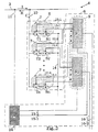
- Circuit arrangement 1 also in the form of a Block diagram shown.
- the circuit arrangement 1 receives 2 in its input area on the input line device 3, which again with the Output line device 21 of an externally transmitting unit 20 is connected, in turn an input signal I, which for Formation of a partially compensated reflection signal R leads.
- the input area 2 of the circuit arrangement 1 is one Protective device 4 with a compensation device 5, the latter via a compensation line 10 a generated compensation signal C in the input line device 3 of the input area 2 feeds.
- the compensation device 5 points to generation and deployment of the compensation signal C a controllable current source device 7 or current source amplification device.
- This current source device 7 or current source amplification device is by means of the control device 6 a control line 22 is supplied with a control signal S.
- control signal S in the control device 6 by sampling the reflection signal R on the input line device 3 by means of the scanning line 11 and the comparison device 8 in the control device 6 generates and realizes.
- control device 6 and / or the comparison device 8 can in particular via external control lines 23 or 24 externally programmable - be controllable.
- FIG. 3 shows a detailed view in a further block diagram a further embodiment of the invention Circuit arrangement 1, with regard to the protective device 4th
- n are independent of each other Power source devices 7 are provided. These are about one common supply line 14 supplied and from each other separate and independent power control lines 12-1, ..., 12-n and also separated from each other and from each other independent switching lines 13-1, ..., 13-n with respect to generating current strength or with regard to their switched-on state controlled.
- each of the current source devices there are 7 in each of the current source devices a transistor T1, ..., Tn is provided for current control, wherein the respective current control lines 12-1, ..., 12-n as Base lines act.
- the switching status is in each case Switching elements S1, ..., Sn, which are also used as transistors can be designed and which with the transistors T1, ..., Tn are connected in series.
- the respective contributions of the individual power source devices 7 are carried out by connecting them in parallel via the compensation line 10 in the protective device 4.
- a register device 9 is provided, which is a first Register R1 and a second register R2, which for controlling the current strengths of the current source devices 7 via the current control lines 12-1, ..., 12-n or Control of the switch-on state of the power source devices 7 provided via the switching lines 13-1, ..., 13-n are.
- the registers R1 and R2 of the register device 9 are in the Control device 6 and are arranged via bus lines 15-1, 15-2 and 16-1, 16-2 with the comparison device 8, with other circuit devices or with the outside world controllably connected.
- the comparison device 8 receives via the scanning line 11 as a controlled variable, the current and / or the voltage of the reflection signal R on the input line device 3 of the input area 2 and then carries out a corresponding comparison operation with a given command or target size, which if necessary via an external control line 24 can be provided or changed by.
- the register device 9 with its registers R1, R2 can be used as so-called mode register serve and - especially externally - be programmable.
Landscapes
- Logic Circuits (AREA)
- Dram (AREA)
- Amplifiers (AREA)
- Semiconductor Memories (AREA)
- Semiconductor Integrated Circuits (AREA)
Applications Claiming Priority (2)
| Application Number | Priority Date | Filing Date | Title |
|---|---|---|---|
| DE10021371A DE10021371A1 (de) | 2000-05-02 | 2000-05-02 | Schaltungsanordnung |
| DE10021371 | 2000-05-02 |
Publications (2)
| Publication Number | Publication Date |
|---|---|
| EP1152425A2 true EP1152425A2 (fr) | 2001-11-07 |
| EP1152425A3 EP1152425A3 (fr) | 2005-01-26 |
Family
ID=7640542
Family Applications (1)
| Application Number | Title | Priority Date | Filing Date |
|---|---|---|---|
| EP01109864A Withdrawn EP1152425A3 (fr) | 2000-05-02 | 2001-04-23 | Dispositif de mémoire |
Country Status (4)
| Country | Link |
|---|---|
| US (1) | US6476658B2 (fr) |
| EP (1) | EP1152425A3 (fr) |
| DE (1) | DE10021371A1 (fr) |
| TW (1) | TW571315B (fr) |
Cited By (1)
| Publication number | Priority date | Publication date | Assignee | Title |
|---|---|---|---|---|
| WO2010048971A1 (fr) * | 2008-10-30 | 2010-05-06 | Verigy (Singapore) Pte., Ltd. | Mécanisme d'essai, broche à effet pogo et procédé pour l'essai d'un dispositif à 'essai |
Citations (1)
| Publication number | Priority date | Publication date | Assignee | Title |
|---|---|---|---|---|
| EP0877482A1 (fr) * | 1992-01-23 | 1998-11-11 | Applied Materials, Inc. | Circuit d'adaptation d'accord électronique comportant un système de commande prédicteur-correcteur |
Family Cites Families (6)
| Publication number | Priority date | Publication date | Assignee | Title |
|---|---|---|---|---|
| US4704573A (en) * | 1985-11-22 | 1987-11-03 | Motorola, Inc. | Impedance mismatch detector |
| SE9400657D0 (sv) * | 1994-02-25 | 1994-02-25 | Ellemtel Utvecklings Ab | En, en kontrollspänning alstrande, krets |
| DE4445846A1 (de) * | 1994-12-22 | 1996-06-27 | Sel Alcatel Ag | Verfahren und Schaltungsanordnung für den Abschluß einer zu einer integrierten CMOS-Schaltung führenden Leitung |
| DE19735982C2 (de) * | 1997-08-19 | 2000-04-27 | Ericsson Telefon Ab L M | Leitungsempfängerschaltkreis mit Leitungsabschlußimpedanz |
| EP0872961B1 (fr) * | 1998-01-15 | 2000-03-29 | Hewlett-Packard Company | Egalisateur d'amplitude pour des lignes de transmission |
| JP2000122761A (ja) * | 1998-10-14 | 2000-04-28 | Hitachi Ltd | バスシステム及びそれを用いたメモリシステム |
-
2000
- 2000-05-02 DE DE10021371A patent/DE10021371A1/de not_active Ceased
-
2001
- 2001-04-23 EP EP01109864A patent/EP1152425A3/fr not_active Withdrawn
- 2001-05-02 US US09/847,673 patent/US6476658B2/en not_active Expired - Lifetime
- 2001-05-31 TW TW090110278A patent/TW571315B/zh not_active IP Right Cessation
Patent Citations (1)
| Publication number | Priority date | Publication date | Assignee | Title |
|---|---|---|---|---|
| EP0877482A1 (fr) * | 1992-01-23 | 1998-11-11 | Applied Materials, Inc. | Circuit d'adaptation d'accord électronique comportant un système de commande prédicteur-correcteur |
Cited By (1)
| Publication number | Priority date | Publication date | Assignee | Title |
|---|---|---|---|---|
| WO2010048971A1 (fr) * | 2008-10-30 | 2010-05-06 | Verigy (Singapore) Pte., Ltd. | Mécanisme d'essai, broche à effet pogo et procédé pour l'essai d'un dispositif à 'essai |
Also Published As
| Publication number | Publication date |
|---|---|
| DE10021371A1 (de) | 2001-11-08 |
| US6476658B2 (en) | 2002-11-05 |
| US20010040476A1 (en) | 2001-11-15 |
| TW571315B (en) | 2004-01-11 |
| EP1152425A3 (fr) | 2005-01-26 |
Similar Documents
| Publication | Publication Date | Title |
|---|---|---|
| DE60112157T2 (de) | Halbleiter-Steuerschaltungsanordnung | |
| DE69620099T2 (de) | Hochfrequenz-Leistungsverstärker | |
| DE2747282C3 (de) | Stufenweise schaltbarer elektrischer Dämpfer | |
| DE2534245C3 (de) | Regelschaltung für piezoelektrische Wandler | |
| DE19725710B4 (de) | Verfahren und Vorrichtung zur Leistungs- und Datenübermittlung auf gemeinsamen Leitungen | |
| DE2953275C2 (fr) | ||
| DE2658222B1 (de) | Geraet zur ultraschallabtastung | |
| DE60128380T2 (de) | Dynamische einstellung für einen spannungshub | |
| DE2629562B1 (de) | Geraet zur ultraschallmessung | |
| DE2809633A1 (de) | Gesteuerter erzeuger von perioden- signalbildern | |
| DE19836997B4 (de) | Sende/Empfangs-Schaltkreis und Sende/Empfangs-Verfahren für einen Wandler | |
| DE2419380B2 (de) | Übertragungssystem | |
| DE1905993B2 (de) | Elektrischer regler, bestehend aus der hintereinanderschaltung eines pidregelverstaerkers und eines diesem vorgeschalteten d-gliedes | |
| EP1371138B1 (fr) | Dispositif de mise en forme d'un signal d'entree pour ligne mal adaptee en sortie | |
| EP3387749B1 (fr) | Commutateur côté haut pour alimenter en courant au moins un capteur | |
| EP1152425A2 (fr) | Dispositif de mémoire | |
| DE60225399T2 (de) | Schaltkreis zur aktiven Entkoppelung von Sendespulen in Kernspinresonanztomographen, insbesondere vom Niedrigfeld-Typus | |
| DE10049994A1 (de) | Schaltungsanordnung zum Überwachen und/oder zum Einstellen von Versorgungsspannungen | |
| DE102004060577B4 (de) | Schaltung und Verfahren zum Erzeugen eines Strompulses in einem Wellenleiter | |
| DE19930358A1 (de) | Schaltungsanordnung zur Signalkopplung zwischen Schaltungsteilen mit voneinander getrennten Versorgungsleitungen | |
| DE3940295C2 (de) | Mobilfunkgerät und Hochfrequenzsender mit geregelter Ausgangsleistung | |
| DE60100929T2 (de) | Treiberschaltung mit einstellbarem Ausgangsstrom | |
| DE2543861A1 (de) | Schaltungsanordnung zur sperrung eines zweirichtungsverstaerkers gegen die aufnahme abgehender signale | |
| DE1762532C3 (de) | Schaltungsanordnung fur die Über tragung von gestörten Impulsen | |
| DE1948257C3 (de) | Verfahren und Anordnung zur Erzeugung eines Zündimpulses mit einer hohen steilen Spitze und einem Impulsrücken |
Legal Events
| Date | Code | Title | Description |
|---|---|---|---|
| PUAI | Public reference made under article 153(3) epc to a published international application that has entered the european phase |
Free format text: ORIGINAL CODE: 0009012 |
|
| AK | Designated contracting states |
Kind code of ref document: A2 Designated state(s): AT BE CH CY DE DK ES FI FR GB GR IE IT LI LU MC NL PT SE TR |
|
| AX | Request for extension of the european patent |
Free format text: AL;LT;LV;MK;RO;SI |
|
| PUAL | Search report despatched |
Free format text: ORIGINAL CODE: 0009013 |
|
| AK | Designated contracting states |
Kind code of ref document: A3 Designated state(s): AT BE CH CY DE DK ES FI FR GB GR IE IT LI LU MC NL PT SE TR |
|
| AX | Request for extension of the european patent |
Extension state: AL LT LV MK RO SI |
|
| RIC1 | Information provided on ipc code assigned before grant |
Ipc: 7H 03H 11/28 B Ipc: 7H 03H 11/30 B Ipc: 7G 06F 13/40 B Ipc: 7G 11C 5/00 A |
|
| 17P | Request for examination filed |
Effective date: 20050701 |
|
| AKX | Designation fees paid |
Designated state(s): DE FR GB IE IT |
|
| 17Q | First examination report despatched |
Effective date: 20050818 |
|
| GRAP | Despatch of communication of intention to grant a patent |
Free format text: ORIGINAL CODE: EPIDOSNIGR1 |
|
| STAA | Information on the status of an ep patent application or granted ep patent |
Free format text: STATUS: THE APPLICATION IS DEEMED TO BE WITHDRAWN |
|
| 18D | Application deemed to be withdrawn |
Effective date: 20080424 |