EP1152425A2 - Memory device - Google Patents
Memory device Download PDFInfo
- Publication number
- EP1152425A2 EP1152425A2 EP01109864A EP01109864A EP1152425A2 EP 1152425 A2 EP1152425 A2 EP 1152425A2 EP 01109864 A EP01109864 A EP 01109864A EP 01109864 A EP01109864 A EP 01109864A EP 1152425 A2 EP1152425 A2 EP 1152425A2
- Authority
- EP
- European Patent Office
- Prior art keywords
- circuit arrangement
- signal
- compensation
- current
- input
- Prior art date
- Legal status (The legal status is an assumption and is not a legal conclusion. Google has not performed a legal analysis and makes no representation as to the accuracy of the status listed.)
- Withdrawn
Links
Images


Classifications
-
- G—PHYSICS
- G11—INFORMATION STORAGE
- G11C—STATIC STORES
- G11C5/00—Details of stores covered by group G11C11/00
- G11C5/06—Arrangements for interconnecting storage elements electrically, e.g. by wiring
- G11C5/063—Voltage and signal distribution in integrated semi-conductor memory access lines, e.g. word-line, bit-line, cross-over resistance, propagation delay
Definitions
- the invention relates to a circuit arrangement according to the Preamble of claim 1.
- Another known measure for protection against reflection signals is the provision of a concentrated resistor in parallel in the entrance area of the circuit arrangement, where the value of the resistance matches the characteristic impedance is chosen, with a strong suppression of training and emission of a reflection signal can be achieved.
- a disadvantage of these known circuit arrangements and protective devices provided therein is that these respective Protective device to partially prevent training and / or emitting reflection signals always on the specific value of that in the input area of the circuit arrangement existing wave resistance is matched. there it is particularly disadvantageous that when changing this The corresponding protective device the changed conditions are no longer set and the Protection can no longer be adequately guaranteed.
- Such Changes in wave resistance in the entrance area known circuit arrangements result e.g. in connection with variations in the production process the circuit arrangement but also by interaction with the electrical system following the circuit arrangement.
- the invention has for its object a circuit arrangement, e.g. a storage device, in particular a To create DRAM element, or the like, in which the Form and / or send out a received on Input signals are based on reflection signals in particular simple but reliable and flexible way and way can be suppressed.
- a circuit arrangement e.g. a storage device, in particular a To create DRAM element, or the like, in which the Form and / or send out a received on Input signals are based on reflection signals in particular simple but reliable and flexible way and way can be suppressed.
- At least one entrance area is provided, which at least for receiving a supplied electrical input signal is formed and which for this purpose at least one input line device having.
- a protective device provided which is formed at the entrance area and which is at least to partially prevent training and / or outputting one fed onto a received one Input signal based reflection signal, in particular is formed on the input line device.
- the circuit arrangement according to the invention is characterized in that that the protective device is an active compensation device has, by which a compensation signal can be generated and / or a developing and / or sent becoming reflection signal is superimposed.
- a basic idea of the present invention is therefore an emerging one instead of passive reflection suppression Reflection signal and / or emitting one already reflection signal generated by suitable superposition, i.e. especially through destructive interference, with a Compensation signal to compensate at least partially.
- passive and fixed protective measures e.g. with fixed series resistors or constant concentrated Parallel resistances
- an adaptation to changing framework conditions not possible due to the fixed choice of components is, the use according to the invention of an actively generated Compensation signal the greatest possible flexibility in suppressing reflections, even if due to varying production conditions and / or due to further interactive circuit arrangements in After the entrance area the apparent wave resistance and thus change the reflection behavior in the entrance area.
- the basic idea of the present invention can also go in that regard be understood that instead of passive reflection suppression an active signal adaptation performed is, the training by consumption of the input signal of a reflection signal prevented or suppressed becomes.
- a active signal matching device is provided, which is just the consumption of the input signal and thus the suppression or preventing the formation of a reflection signal.
- an active signal matching device under the active compensation device, through which a compensation signal can be generated and a forming reflection signal is superimposed, always an active signal matching device can be understood, which the formation of a Reflection signal prevented.
- the compensation device is controllable, especially in the frame a feedback control circuit.
- this measure can e.g. can be achieved via appropriate sensors the actual formation and / or transmission of a reflection signal permanently monitored at given times then in the presence of a certain threshold a corresponding adaptation of the compensation signal in the reflection signal both in terms of time and amplitude - if necessary - instantly.
- Circuit arrangement at least one controlled variable, in particular a voltage and / or a current, in particular of the input line device on which the reflection wave or the reflection signal to the original transmitting Unit would run back, the compensation device and / or supplied to the control device.
- At least one, in particular controllable, power source device provided that also as a current source amplification device can be understood.
- a control signal becomes a corresponding one in the power source device Current signal for superimposition with a reflection signal that is developing generated and in particular the input line device provided.
- control device has a comparison device which for comparison a supplied controlled variable with a specified reference variable or target size and for generating and providing a comparison signal and / or control signal, in particular to the compensation device.
- the control variable supplied can be particularly important around one in the entrance area and in particular in the entrance line device measured value of the present current electrical current or an electrical current Act tension.
- the leadership role would correspond to one Setpoint or threshold value for the electrical voltage or the electrical current, which in the entrance area through the Reflection wave must not be exceeded.
- the comparison to be carried out in the comparison device determined whether the corresponding thresholds be crossed, be exceeded, be passed. In response to being exceeded currently and instantly a corresponding comparison signal and / or control signal generated and in particular to the compensation device issued, which also instantaneously a corresponding compensation of the reflection signal takes place.
- a particularly advantageous embodiment of the invention Circuit arrangement arises when the compensation device has a plurality of power source devices, the control device has a register device and the register device for selecting and / or determining the active and / or the current source devices to be activated and / or the respective current gains is trained.
- the register device in each case active and / or to be activated current source devices to be selected. It is therefore possible to have several possibly also identical current sources in the compensation device, e.g. via appropriate switches. Depending on the strength of the reflection signal that forms then become one or more of these power sources, which are connected in parallel, so that each one Power source their individual contribution to building and superimposing of the compensation signal with the reflection signal generated and provided.
- the register device too the corresponding amplification factors of the individual current sources can be controlled, e.g. via an appropriate feed Gate / base voltage if the respective current sources e.g. b. designed as bipolar or field effect transistors are.
- a further increase in flexibility and reliability the compensation of reflection signals results if the Comparison device and / or the register device, in particular are external, programmable. Thereby can namely the threshold values which are exceeded for a readjustment of the compensation behavior and the Compensation signal lead, be adjusted. Furthermore, a programmable register device can also be used to the behavior of the compensation device afterwards adapt and optimize.
- the input area 2 of the circuit arrangement is connected via an input line device 3 to an external transmitting device 20 and its output line device 21, via which an input signal I is transmitted to the circuit arrangement 1 according to the invention becomes.
- a backward reflection signal R then forms due to the mismatch of the input capacitance C rec to the given wave impedance Z 1 , which returns via the input line device 3 to the output line device 21 of the transmitting unit 20.
- one Protective device 4 is provided, which via a compensation line 10 one of a as a compensation device 5 serving controlled current source device 7 generated Compensation signal C to the input line device 3 to compensate for the reflection signal R provides.
- the arrow C opposite arrow I shortened arrow R may indicate this partial compensation.
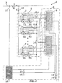
- Circuit arrangement 1 also in the form of a Block diagram shown.
- the circuit arrangement 1 receives 2 in its input area on the input line device 3, which again with the Output line device 21 of an externally transmitting unit 20 is connected, in turn an input signal I, which for Formation of a partially compensated reflection signal R leads.
- the input area 2 of the circuit arrangement 1 is one Protective device 4 with a compensation device 5, the latter via a compensation line 10 a generated compensation signal C in the input line device 3 of the input area 2 feeds.
- the compensation device 5 points to generation and deployment of the compensation signal C a controllable current source device 7 or current source amplification device.
- This current source device 7 or current source amplification device is by means of the control device 6 a control line 22 is supplied with a control signal S.
- control signal S in the control device 6 by sampling the reflection signal R on the input line device 3 by means of the scanning line 11 and the comparison device 8 in the control device 6 generates and realizes.
- control device 6 and / or the comparison device 8 can in particular via external control lines 23 or 24 externally programmable - be controllable.
- FIG. 3 shows a detailed view in a further block diagram a further embodiment of the invention Circuit arrangement 1, with regard to the protective device 4th
- n are independent of each other Power source devices 7 are provided. These are about one common supply line 14 supplied and from each other separate and independent power control lines 12-1, ..., 12-n and also separated from each other and from each other independent switching lines 13-1, ..., 13-n with respect to generating current strength or with regard to their switched-on state controlled.
- each of the current source devices there are 7 in each of the current source devices a transistor T1, ..., Tn is provided for current control, wherein the respective current control lines 12-1, ..., 12-n as Base lines act.
- the switching status is in each case Switching elements S1, ..., Sn, which are also used as transistors can be designed and which with the transistors T1, ..., Tn are connected in series.
- the respective contributions of the individual power source devices 7 are carried out by connecting them in parallel via the compensation line 10 in the protective device 4.
- a register device 9 is provided, which is a first Register R1 and a second register R2, which for controlling the current strengths of the current source devices 7 via the current control lines 12-1, ..., 12-n or Control of the switch-on state of the power source devices 7 provided via the switching lines 13-1, ..., 13-n are.
- the registers R1 and R2 of the register device 9 are in the Control device 6 and are arranged via bus lines 15-1, 15-2 and 16-1, 16-2 with the comparison device 8, with other circuit devices or with the outside world controllably connected.
- the comparison device 8 receives via the scanning line 11 as a controlled variable, the current and / or the voltage of the reflection signal R on the input line device 3 of the input area 2 and then carries out a corresponding comparison operation with a given command or target size, which if necessary via an external control line 24 can be provided or changed by.
- the register device 9 with its registers R1, R2 can be used as so-called mode register serve and - especially externally - be programmable.
Landscapes
- Logic Circuits (AREA)
- Dram (AREA)
- Amplifiers (AREA)
- Semiconductor Memories (AREA)
- Semiconductor Integrated Circuits (AREA)
Abstract
Description
Die Erfindung betrifft eine Schaltungsanordnung gemäß dem
Oberbegriff des Anspruchs 1.The invention relates to a circuit arrangement according to the
Preamble of
Bei vielen elektrischen Systemen und Schaltungsanordnungen werden bestimmte Signale von Teilen des Systems, z.B. sogenannten Treibern, ausgesandt und an andere Teile des Systems, sogenannte Empfänger oder Receiver, bereitgestellt und übertragen. Problematisch bei elektrischen Systemen, Schaltungsanordnungen, z.B. Speichereinrichtungen, insbesondere DRAM-Elementen, ist dabei, daß in vielen Fällen - insbesondere wenn die Eingangsimpedanz hochohmig und hauptsächlich kapazitiv ausgelegt ist - aufgrund des Wellenwiderstandes des Eingangsbereichs eines derartigen elektrischen Systems oder einer Schaltungsanordnung eine im Eingangsbereich dieses Systems oder der Schaltungsanordnung eintreffende Signalflanke oder Spannungsflanke zumindest teilweise, oft jedoch totalreflektiert wird. Das reflektierte Signal oder Reflexionssignal läuft dann aus dem Eingangsbereich der empfangenden Schaltungsanordnung aus und auf die sendende Einheit hin zurück. Das Reflexionssignal kann dann dort und/oder darüber hinaus zu einer Fehlfunktion und somit insgesamt zu einer gesamten Fehlfunktion des elektrischen Systems führen.With many electrical systems and circuit arrangements certain signals from parts of the system, e.g. so-called Drivers, sent out and to other parts of the system, so-called receivers, provided and transmitted. Problematic with electrical systems, circuit arrangements, e.g. Memory devices, in particular DRAM elements, is doing that in many cases - especially if the input impedance is high impedance and mainly capacitive is designed - due to the wave resistance of the input area such an electrical system or Circuit arrangement one in the entrance area of this system or the signal edge arriving on the circuit arrangement or voltage edge at least partially, but often totally reflected becomes. The reflected signal or reflection signal then runs out of the input area of the receiving circuit arrangement and back to the sending unit. The reflection signal can then be there and / or beyond to a malfunction and thus to a total Malfunction of the electrical system.
Bei bekannten Schaltungsanordnungen, gerade auch bei Speichereinrichtungen, insbesondere bei DRAM-Elementen, wurden daher vielfältige Maßnahmen vorgeschlagen, um das Ausbilden und/ oder das Aussenden von auf Eingangssignalen beruhenden Reflexionssignalen zu unterbinden.In known circuit arrangements, especially in the case of storage devices, especially with DRAM elements therefore various measures proposed to train and / or sending out based on input signals Prevent reflection signals.
Es wurden z.B. Schutzeinrichtungen vorgeschlagen, die an den spezifischen Eingangs-/Wellenwiderstand des Eingangsbereichs der Schaltungsanordnung angepaßt sind und im Hinblick auf den konkreten Wellenwiderstand des Eingangsbereichs zumindest zu einer teilweisen Unterdrückung eines Reflexionssignales führen.For example, Protective devices proposed to the specific input / wave resistance of the input range the circuit arrangement are adapted and with regard to the concrete wave impedance of the entrance area at least partial suppression of a reflection signal.
Bekannte derartige Schutzeinrichtungen in Schaltungsanordnungen sehen z.B. Vorwiderstände zum Dämpfen des rücklaufenden Reflexionssignals vor. Dadurch werden zum einen die einlaufende Welle und zum anderen nach Reflexion auch die auslaufende Welle und somit die zurücktransportierte Leistung gedämpft.Known protective devices of this type in circuit arrangements see e.g. Series resistors to dampen the return Reflection signal before. On the one hand, this means that the incoming Wave and on the other hand after reflection also the expiring Wave and thus dampened the returned power.
Eine andere bekannte Maßnahme zum Schutz vor Reflexionssignalen ist das Vorsehen eines konzentrierten Widerstands in Parallelschaltung im Eingangsbereich der Schaltungsanordnung, wobei der Wert des Widerstands passend zum Wellenwiderstand gewählt wird, wobei eine starke Unterdrückung des Ausbildens und Aussendens eines Reflexionssignals erreicht werden kann.Another known measure for protection against reflection signals is the provision of a concentrated resistor in parallel in the entrance area of the circuit arrangement, where the value of the resistance matches the characteristic impedance is chosen, with a strong suppression of training and emission of a reflection signal can be achieved.
Nachteilig bei diesen bekannten Schaltungsanordnungen und den darin vorgesehenen Schutzeinrichtungen ist, daß diese jeweilige Schutzeinrichtung zum teilweisen Unterbinden des Ausbildens und/oder Aussendens von Reflexionssignalen immer auf den spezifischen Wert des im Eingangsbereich der Schaltungsanordnung vorliegenden Wellenwiderstandes abgestimmt ist. Dabei ist es insbesondere nachteilig, daß bei einer Änderung dieses Wellenwiderstandes die entsprechende Schutzeinrichtung auf die veränderten Bedingungen nicht mehr eingestellt und der Schutz nicht mehr ausreichend gewährleistet werden kann. Derartige Änderungen des Wellenwiderstands im Eingangsbereich bekannter Schaltungsanordnungen ergeben sich z.B. im Zusammenhang mit Variationen im Rahmen des Produktionsprozesses der Schaltungsanordnung aber auch durch Wechselwirkung mit der Schaltungsanordnung nachfolgenden elektrischen Systemen.A disadvantage of these known circuit arrangements and protective devices provided therein is that these respective Protective device to partially prevent training and / or emitting reflection signals always on the specific value of that in the input area of the circuit arrangement existing wave resistance is matched. there it is particularly disadvantageous that when changing this The corresponding protective device the changed conditions are no longer set and the Protection can no longer be adequately guaranteed. Such Changes in wave resistance in the entrance area known circuit arrangements result e.g. in connection with variations in the production process the circuit arrangement but also by interaction with the electrical system following the circuit arrangement.
Der Erfindung liegt die Aufgabe zugrunde, eine Schaltungsanordnung, z.B. eine Speichereinrichtung, insbesondere ein DRAM-Element, oder dergleichen zu schaffen, bei welchem das Ausbilden und/oder Aussenden eines auf empfangenen zugeführten Eingangssignalen beruhenden Reflexionssignales auf besonders einfache aber gleichwohl zuverlässige und flexible Art und Weise unterdrückt werden kann.The invention has for its object a circuit arrangement, e.g. a storage device, in particular a To create DRAM element, or the like, in which the Form and / or send out a received on Input signals are based on reflection signals in particular simple but reliable and flexible way and way can be suppressed.
Die Aufgabe wird erfindungsgemäß mit einer gattungsgemäßen
Schaltungsanordnung durch die kennzeichnenden Merkmale des
Anspruchs 1 gelöst. Vorteilhafte Weiterbildungen der erfindungsgemäßen
Schaltungsanordnung sind Gegenstand der abhängigen
Unteransprüche.The object is achieved with a generic
Circuit arrangement by the characteristic features of the
Bei der gattungsgemäßen Schaltungsanordnung, z.B. Speichereinrichtung, insbesondere DRAM-Element, oder dergleichen ist mindestens ein Eingangsbereich vorgesehen, welcher zumindest zum Empfang eines zugeführten elektrischen Eingangssignals ausgebildet ist und welcher dazu mindestens eine Eingangsleitungseinrichtung aufweist. Ferner ist eine Schutzeinrichtung vorgesehen, welche am Eingangsbereich ausgebildet ist und welche zumindest zum teilweisen Unterbinden des Ausbildens und/oder Ausgebens eines auf einem empfangenen zugeführten Eingangssignal beruhenden Reflexionssignals, insbesondere auf der Eingangsleitungseinrichtung, ausgebildet ist.In the generic circuit arrangement, e.g. Storage device, especially DRAM element, or the like At least one entrance area is provided, which at least for receiving a supplied electrical input signal is formed and which for this purpose at least one input line device having. There is also a protective device provided which is formed at the entrance area and which is at least to partially prevent training and / or outputting one fed onto a received one Input signal based reflection signal, in particular is formed on the input line device.
Die erfindungsgemäße Schaltungsanordnung ist dadurch gekennzeichnet, daß die Schutzeinrichtung eine aktive Kompensationseinrichtung aufweist, durch welche ein Kompensationssignal generierbar und/oder einem sich ausbildenden und/oder ausgesandt werdenden Reflexionssignal überlagerbar ist.The circuit arrangement according to the invention is characterized in that that the protective device is an active compensation device has, by which a compensation signal can be generated and / or a developing and / or sent becoming reflection signal is superimposed.
Eine Grundidee der vorliegenden Erfindung besteht also darin, anstelle einer passiven Reflexionsunterdrückung ein entstehendes Reflexionssignal und/oder das Aussenden eines bereits entstandenen Reflexionssignals durch geeignete Superposition, d.h. insbesondere durch destruktive Interferenz, mit einem Kompensationssignal zumindest teilweise zu kompensieren. Während bei passiven und fest gewählten Schutzmaßnahmen, z.B. bei festen Vorwiderständen oder konstanten konzentrierten Parallelwiderständen, eine Anpassung an sich ändernde Rahmenbedingungen aufgrund der festen Wahl der Bauteile nicht möglich ist, bietet der erfindungsgemäße Einsatz eines aktiv generierten Kompensationssignals eine größtmögliche Flexibilität bei der Unterdrückung von Reflexionen, auch dann, wenn sich aufgrund variierender Produktionsbedingungen und/oder aufgrund weiterer wechselwirkender Schaltungsanordnungen im Nachgang zum Eingangsbereich der apparente Wellenwiderstand und somit das Reflexionsverhalten im Eingangsbereich ändern.A basic idea of the present invention is therefore an emerging one instead of passive reflection suppression Reflection signal and / or emitting one already reflection signal generated by suitable superposition, i.e. especially through destructive interference, with a Compensation signal to compensate at least partially. While for passive and fixed protective measures, e.g. with fixed series resistors or constant concentrated Parallel resistances, an adaptation to changing framework conditions not possible due to the fixed choice of components is, the use according to the invention of an actively generated Compensation signal the greatest possible flexibility in suppressing reflections, even if due to varying production conditions and / or due to further interactive circuit arrangements in After the entrance area the apparent wave resistance and thus change the reflection behavior in the entrance area.
Die Grundidee der vorliegenden Erfindung kann auch dahingehend aufgefaßt werden, daß anstelle einer passiven Reflexionsunterdrückung eine aktive Signalanpassung durchgeführt wird, wobei durch Verbrauch des Eingangssignals die Ausbildung eines Reflexionssignals verhindert oder unterdrückt wird. Dies wird erfindungsgemäß dadurch erreicht, daß eine aktive Signalanpaßeinrichtung vorgesehen ist, welche gerade den Verbrauch des Eingangssignals und somit die Unterdrückung oder Verhinderung der Ausbildung eines Reflexionssignals realisiert.The basic idea of the present invention can also go in that regard be understood that instead of passive reflection suppression an active signal adaptation performed is, the training by consumption of the input signal of a reflection signal prevented or suppressed becomes. This is achieved according to the invention in that a active signal matching device is provided, which is just the consumption of the input signal and thus the suppression or preventing the formation of a reflection signal.
Nachfolgend soll unter der aktiven Kompensationseinrichtung, durch welche ein Kompensationssignal generierbar und einem sich ausbildenden Reflexionssignal überlagerbar ist, auch immer eine aktive Signalanpaßeinrichtung verstanden werden, welche durch Verbrauch des Eingangssignals die Ausbildung eines Reflexionssignals verhindert.In the following, under the active compensation device, through which a compensation signal can be generated and a forming reflection signal is superimposed, always an active signal matching device can be understood, which the formation of a Reflection signal prevented.
Dabei ist es von besonderem Vorteil, wenn die Kompensationseinrichtung steuerbar ausgebildet ist, insbesondere im Rahmen eines Rückkopplungssteuerkreises. Mit dieser Maßnahme kann z.B. erreicht werden, daß über eine entsprechende Sensorik das tatsächliche Ausbilden und/oder Aussenden eines Reflexionssignals permanent und zu gegebenen Zeitpunkten überwacht wird, um dann beim Vorliegen eines bestimmten Schwellenwertes im Reflexionssignal eine entsprechende Anpassung des Kompensationssignals sowohl zeitlich als auch amplitudenmäßig - ggf. instantan - vorzunehmen. It is particularly advantageous if the compensation device is controllable, especially in the frame a feedback control circuit. With this measure can e.g. can be achieved via appropriate sensors the actual formation and / or transmission of a reflection signal permanently monitored at given times then in the presence of a certain threshold a corresponding adaptation of the compensation signal in the reflection signal both in terms of time and amplitude - if necessary - instantly.
Dazu ist es vorteilhaft, wenn zur Steuerung der Kompensationseinrichtung eine entsprechende Steuereinrichtung, insbesondere im Eingangsbereich der Schaltungsanordnung, vorgesehen ist.To this end, it is advantageous if to control the compensation device a corresponding control device, in particular provided in the entrance area of the circuit arrangement is.
Zur Ausführung der Steuerung der Kompensationseinrichtung wird in einer bevorzugten Ausführungsform der erfindungsgemäßen Schaltungsanordnung mindestens eine Regelgröße, insbesondere eine Spannung und/oder ein Strom, insbesondere von der Eingangsleitungseinrichtung, auf welcher die Reflexionswelle oder das Reflexionssignal zur ursprünglich sendenden Einheit zurücklaufen würde, der Kompensationseinrichtung und/oder der Steuereinrichtung zugeführt.To carry out the control of the compensation device is in a preferred embodiment of the invention Circuit arrangement at least one controlled variable, in particular a voltage and / or a current, in particular of the input line device on which the reflection wave or the reflection signal to the original transmitting Unit would run back, the compensation device and / or supplied to the control device.
Zur Ausbildung des Kompensationssignals ist in einer weiteren Ausführungsform der erfindungsgemäßen Schaltungsanordnung mindestens eine, insbesondere steuerbare, Stromquelleneinrichtung vorgesehen, die auch als Stromquellenverstärkungseinrichtung aufgefaßt werden kann. Auf ein Steuersignal hin wird somit in der Stromquelleneinrichtung ein entsprechendes Stromsignal zur Überlagerung mit einem sich ausbildenden Reflexionssignal generiert und insbesondere der Eingangsleitungseinrichtung bereitgestellt.Another is to form the compensation signal Embodiment of the circuit arrangement according to the invention at least one, in particular controllable, power source device provided that also as a current source amplification device can be understood. In response to a control signal becomes a corresponding one in the power source device Current signal for superimposition with a reflection signal that is developing generated and in particular the input line device provided.
Dabei ist es von besonderem Vorteil, wenn die Stromquelleneinrichtung
zu einer Stromgenerierung und/oder -verstärkung
ausgebildet ist, welche einem gegebenen Wellenwiderstand,
insbesondere des Eingangsbereichs der Schaltungsanordnung,
angepaßt ist und welche insbesondere die Beziehung
Zur besonders effektiven Ausführung des Unterdrückens und/ oder Unterbindens eines Reflexionssignals ist es bei der erfindungsgemäßen Schaltungsanordnung gemäß einer weiteren vorteilhaften Ausführungsform vorgesehen, daß die Steuereinrichtung eine Vergleichseinrichtung aufweist, welche zum Vergleichen einer zugeführten Regelgröße mit einer vorgegebenen Führungsgröße oder Sollgröße und zum Generieren und Bereitstellen eines Vergleichssignals und/oder Steuersignals, insbesondere an die Kompensationseinrichtung, ausgebildet ist.For particularly effective execution of suppression and / or preventing a reflection signal, it is in the case of the invention Circuit arrangement according to a further advantageous Embodiment provided that the control device has a comparison device which for comparison a supplied controlled variable with a specified reference variable or target size and for generating and providing a comparison signal and / or control signal, in particular to the compensation device.
Bei der zugeführten Regelgröße kann es sich dabei insbesondere um einen im Eingangsbereich und insbesondere in der Eingangsleitungseinrichtung gemessenen Wert des dort vorliegenden aktuellen elektrischen Stroms oder einer elektrischen Spannung handeln. Die Führungsgröße entspräche dabei einem Sollwert oder Schwellenwert für die elektrische Spannung oder den elektrischen Strom, welcher im Eingangsbereich durch die Reflexionswelle nicht überschritten werden darf.The control variable supplied can be particularly important around one in the entrance area and in particular in the entrance line device measured value of the present current electrical current or an electrical current Act tension. The leadership role would correspond to one Setpoint or threshold value for the electrical voltage or the electrical current, which in the entrance area through the Reflection wave must not be exceeded.
Durch den auszuführenden Vergleich wird in der Vergleichseinrichtung festgestellt, ob die entsprechenden Schwellenwerte überschritten werden. Als Reaktion auf ein Überschreiten wird aktuell und instantan ein entsprechendes Vergleichssignal und/oder Steuersignal generiert und insbesondere an die Kompensationseinrichtung ausgegeben, wodurch ebenfalls instantan eine entsprechende Kompensation des Reflexionssignals erfolgt.The comparison to be carried out in the comparison device determined whether the corresponding thresholds be crossed, be exceeded, be passed. In response to being exceeded currently and instantly a corresponding comparison signal and / or control signal generated and in particular to the compensation device issued, which also instantaneously a corresponding compensation of the reflection signal takes place.
Eine besonders vorteilhafte Ausbildung der erfindungsgemäßen Schaltungsanordnung ergibt sich, wenn die Kompensationseinrichtung eine Mehrzahl von Stromquelleneinrichtungen aufweist, die Steuereinrichtung eine Registereinrichtung aufweist und die Registereinrichtung zum Auswählen und/oder Bestimmen der aktiven und/oder der zu aktivierenden Stromquelleneinrichtungen und/oder der jeweiligen Stromverstärkungen ausgebildet ist.A particularly advantageous embodiment of the invention Circuit arrangement arises when the compensation device has a plurality of power source devices, the control device has a register device and the register device for selecting and / or determining the active and / or the current source devices to be activated and / or the respective current gains is trained.
Durch die vorgesehene Mehrzahl von Stromquelleneinrichtungen ist eine besonders einfache, flexible und schnelle Anpassung des Kompensationssignals an das sich ausbildende Reflexions-signal möglich. Dabei können über die Registereinrichtung die jeweils aktiven und/oder zu aktivierenden Stromquelleneinrichtungen ausgewählt werden. Es ist somit möglich, mehrere, gegebenenfalls auch identische, Stromquellen in der Kompensationseinrichtung, z.B. über entsprechende Schalter, vorzusehen. Je nach Stärke des sich ausbildenden Reflexionssignals werden dann eine oder mehrere dieser Stromquellen, welche parallel geschaltet sind, aktiviert, so daß jede einzelne Stromquelle ihren einzelnen Beitrag zum Aufbau und zur Überlagerung des Kompensationssignals mit dem Reflexionssignal generiert und bereitstellt. Andererseits oder zusätzlich kann daran gedacht werden, daß durch die Registereinrichtung auch die entsprechenden Verstärkungsfaktoren der einzelnen Stromquellen gesteuert werden, z.B. über eine entsprechende zuzuführende Gate-/Basis-Spannung, falls die jeweiligen Stromquellen z. b. als Bipolar- oder Feldeffekttransistoren ausgebildet sind.Through the intended plurality of power source devices is a particularly simple, flexible and quick adjustment of the compensation signal to the reflection signal that forms possible. You can use the register device in each case active and / or to be activated current source devices to be selected. It is therefore possible to have several possibly also identical current sources in the compensation device, e.g. via appropriate switches. Depending on the strength of the reflection signal that forms then become one or more of these power sources, which are connected in parallel, so that each one Power source their individual contribution to building and superimposing of the compensation signal with the reflection signal generated and provided. On the other hand or in addition be remembered that by the register device too the corresponding amplification factors of the individual current sources can be controlled, e.g. via an appropriate feed Gate / base voltage if the respective current sources e.g. b. designed as bipolar or field effect transistors are.
Eine weitere Steigerung der Flexibilität und Zuverlässigkeit der Kompensation von Reflexionssignalen ergibt sich, wenn die Vergleichseinrichtung und/oder die Registereinrichtung, insbesondere extern, programmierbar ausgebildet sind. Dadurch können nämlich die Schwellenwerte, welche beim Überschreiten zu einer Nachregelung des Kompensationsverhaltens und des Kompensationssignals führen, angepaßt werden. Ferner kann eine programmierbare Registereinrichtung auch dazu genutzt werden, das Verhalten der Kompensationseinrichtung auch im Nachhinein anzupassen und zu optimieren.A further increase in flexibility and reliability the compensation of reflection signals results if the Comparison device and / or the register device, in particular are external, programmable. Thereby can namely the threshold values which are exceeded for a readjustment of the compensation behavior and the Compensation signal lead, be adjusted. Furthermore, a programmable register device can also be used to the behavior of the compensation device afterwards adapt and optimize.
Nachfolgend wird die Erfindung anhand einer schematischen Zeichnung auf der Grundlage bevorzugter Ausführungsbeispiele der erfindungsgemäßen Schaltungsanordnung weiter erläutert. In dieser zeigt
- Fig. 1
- in Form eines Blockdiagramms ein erstes Ausführungsbeispiel der erfindungsgemäßen Schaltungsanordnung,
- Fig. 2
- in Form eines Blockdiagramms ein zweites Ausführungsbeispiel der erfindungsgemäßen Schaltungsanordnung,
- Fig. 3
- in Form eines Blockdiagramms eine Kompensationseinrichtung in einem dritten Ausführungsbeispiel der erfindungsgemäßen Schaltungsanordnung und
- Fig. 4
- in Form eines Blockdiagramms eine Schaltungsanordnung aus dem Stand der Technik.
- Fig. 1
- in the form of a block diagram, a first exemplary embodiment of the circuit arrangement according to the invention,
- Fig. 2
- in the form of a block diagram, a second exemplary embodiment of the circuit arrangement according to the invention,
- Fig. 3
- in the form of a block diagram a compensation device in a third embodiment of the circuit arrangement according to the invention and
- Fig. 4
- in the form of a block diagram, a circuit arrangement from the prior art.
In dem in Fig. 1 in Form eines Blockdiagramms dargestellten
ersten Ausführungsbeispiel der erfindungsgemäßen Schaltungsanordnung
1 ist der Eingangsbereich 2 der Schaltungsanordnung
über eine Eingangsleitungseinrichtung 3 mit einer externen
sendenden Einrichtung 20 und deren Ausgangsleitungseinrichtung
21 verbunden, über welche ein Eingangssignal I an die
erfindungsgemäße Schaltungsanordnung 1 übertragen wird. Im
hier hochohmigen Eingangsbereich 2 der Schaltungsanordnung 1
bildet sich dann aufgrund der Fehlanpassung der Eingangskapazität
Crec an die gegebene Wellenimpedanz Z1 ein rücklaufendes
Reflexionssignal R aus, welches über die Eingangsleitungseinrichtung
3 zur Ausgangsleitungseinrichtung 21 der sendenden
Einheit 20 zurückläuft.In the first exemplary embodiment of the
Im Eingangsbereich 2 der Schaltungsanordnung 1 ist eine
Schutzeinrichtung 4 vorgesehen, welche über eine Kompensationsleitung
10 ein von einer als Kompensationseinrichtung 5
dienenden gesteuerten Stromquelleneinrichtung 7 generiertes
Kompensationssignal C an die Eingangsleitungseinrichtung 3
zur Kompensation des sich ausbildenden Reflexionssignals R
bereitstellt. Der durch den Pfeil C gegenüber den Pfeil I
verkürzte Pfeil R mag diese teilweise Kompensation andeuten.In the
In der Fig. 2 ist ein zweites Ausführungsbeispiel der erfindungsgemäßen
Schaltungsanordnung 1 ebenfalls in Form eines
Blockdiagramms gezeigt.2 is a second embodiment of the
Die Schaltungsanordnung 1 empfängt in ihrem Eingangsbereich 2
auf der Eingangsleitungseinrichtung 3, welche wieder mit der
Ausgangsleitungseinrichtung 21 einer extern sendenden Einheit
20 verbunden ist, wiederum ein Eingangssignal I, welche zur
Ausbildung eines teilkompensierten Reflexionssignals R führt.The
Im Eingangsbereich 2 der Schaltungsanordnung 1 ist eine
Schutzeinrichtung 4 mit einer Kompensationseinrichtung 5 ausgebildet,
wobei letztere über eine Kompensationsleitung 10
ein generiertes Kompensationssignal C in die Eingangsleitungseinrichtung
3 des Eingangsbereichs 2 einspeist. Die Kompensationseinrichtung
5 weist zur Generierung und Bereitstellung
des Kompensationssignals C eine steuerbare Stromquelleneinrichtung
7 oder Stromquellenverstärkungseinrichtung auf.
Diese Stromquelleneinrichtung 7 oder Stromquellenverstärkungseinrichtung
wird über die Steuereinrichtung 6 mittels
einer Steuerleitung 22 mit einem Steuersignal S beaufschlagt.In the
In dem in Fig. 2 gezeigten Ausführungsbeispiel wird das Steuersignal
S in der Steuereinrichtung 6 durch Abtasten des Reflexionssignals
R auf der Eingangsleitungseinrichtung 3 mittels
der Abtastleitung 11 und der Vergleichseinrichtung 8 in
der Steuereinrichtung 6 erzeugt und realisiert.In the embodiment shown in Fig. 2, the control signal
S in the
Die Steuereinrichtung 6 und/oder die Vergleichseinrichtung 8
können über externe Steuerleitungen 23 bzw. 24 - insbesondere
extern programmierbar - steuerbar sein.The
Fig. 3 zeigt in einem weiteren Blockdiagramm eine Detailansicht
einer weiteren Ausführungsform der erfindungsgemäßen
Schaltungsanordnung 1, und zwar im Hinblick auf die Schutzeinrichtung
4.3 shows a detailed view in a further block diagram
a further embodiment of the
Bei diesem Ausführungsbeispiel sind n voneinander unabhängige
Stromquelleneinrichtungen 7 vorgesehen. Diese werden über eine
gemeinsame Versorgungsleitung 14 versorgt und über voneinander
getrennte und unabhängige Stromsteuerleitungen 12-1,
..., 12-n und ebenso voneinander getrennte und voneinander
unabhängige Schaltleitungen 13-1, ..., 13-n bezüglich der zu
erzeugenden Stromstärke bzw. bezüglich ihres Einschaltzustandes
gesteuert.In this embodiment, n are independent of each other
Dazu sind in jeder der Stromquelleneinrichtungen 7 jeweils ein Transistor T1, ..., Tn zur Stromsteuerung vorgesehen, wobei die jeweiligen Stromsteuerleitungen 12-1, ..., 12-n als Basisleitungen fungieren. Der Schaltzustand wird jeweils über Schaltelemente S1, ..., Sn, welche ebenfalls als Transistoren ausgelegt sein können und welche mit den Transistoren T1, ..., Tn jeweils in Serie geschaltet sind, geregelt.For this purpose, there are 7 in each of the current source devices a transistor T1, ..., Tn is provided for current control, wherein the respective current control lines 12-1, ..., 12-n as Base lines act. The switching status is in each case Switching elements S1, ..., Sn, which are also used as transistors can be designed and which with the transistors T1, ..., Tn are connected in series.
Anstelle der Transistoren T1, ..., Tn können ganz allgemeine, insbesondere gesteuerte, Stromquelleneinrichtungen vorgesehen sein. In Fig. 3 wären dann die entsprechenden Trabnsistorsymbole durch Symbole für eine allgemeine Stromquelle zu ersetzen. Instead of the transistors T1, ..., Tn, very general, in particular controlled, power source devices are provided his. 3 would then be the corresponding trench transistor symbols to be replaced by symbols for a general power source.
Die jeweiligen Beiträge der einzelnen Stromquelleneinrichtungen
7 erfolgen durch Parallelschaltung über die Kompensationsleitung
10 in der Schutzeinrichtung 4.The respective contributions of the individual
Es ist eine Registereinrichtung 9 vorgesehen, welche ein erstes
Register R1 und ein zweites Register R2 aufweist, die
zur Steuerung der Stromstärken der Stromquelleneinrichtungen
7 über die Stromsteuerleitungen 12-1, ..., 12-n bzw. zur
Steuerung des Einschaltzustandes der Stromquelleneinrichtungen
7 über die Schaltleitungen 13-1, ..., 13-n vorgesehen
sind.A
Die Register R1 und R2 der Registereinrichtung 9 sind in der
Steuereinrichtung 6 angeordnet und werden über Busleitungen
15-1, 15-2 und 16-1, 16-2 mit der Vergleichseinrichtung 8,
mit anderen Schaltungseinrichtungen bzw. mit der Außenwelt
steuerbar verbunden.The registers R1 and R2 of the
Die Vergleichseinrichtung 8 ihrerseits empfängt über die Abtastleitung
11 als Regelgröße den Strom und/oder die Spannung
des Reflexionssignals R auf der Eingangsleitungseinrichtung 3
des Eingangsbereichs 2 und führt dann eine entsprechende Vergleichsoperation
mit einer vorgegebenen Führungs- oder Sollgröße,
welche gegebenenfalls über eine externe Steuerleitung
24 bereitgestellt oder verändert werden kann, durch.The
Die Registereinrichtung 9 mit ihren Registern R1, R2 kann als
sogenanntes Modusregister dienen und - insbesondere extern -
programmierbar sein.The
Fig. 4 zeigt ebenfalls in Form eines Blockdiagramms eine
Schaltungsanordnung 40 aus dem Stand der Technik, wobei im
Eingangsbereich 2 der Schaltungsanordnung 40 eine Schutzeinrichtung
4 vorgesehen ist, welche hier ausschließlich aus einem
passiven parallel geschalteten konzentrierten Widerstand
41 besteht, welcher im Zusammenhang mit der Eingangskapazität
Crec des Eingangsbereichs 2 so gewählt ist, daß sich das aufgrund
des über die Eingangsleitungseinrichtung 3 empfangenen
Eingangssignals Isource ausbildende Reflexionssignal R bei gegebenem
und festem Wellenwiderstand Z1 = Urec/Isource bestmöglich
unterdrücken läßt.FIG. 4 also shows in the form of a block diagram a
Claims (10)
dadurch gekennzeichnet, daß die Kompensationseinrichtung (5), insbesondere rückgekoppelt, steuerbar ausgebildet ist.Circuit arrangement according to claim 1,
characterized in that the compensation device (5), in particular feedback, is designed to be controllable.
dadurch gekennzeichnet, daß zur Steuerung der Kompensationseinrichtung (5) eine Steuereinrichtung (6) vorgesehen ist.Circuit arrangement according to one of claims 1 or 2,
characterized in that a control device (6) is provided for controlling the compensation device (5).
dadurch gekennzeichnet, daß zur Steuerung der Kompensationseinrichtung (5) mindestens eine Regelgröße, insbesondere eine Spannung und/oder ein Strom, insbesondere von der Eingangsleitungseinrichtung (3), der Kompensationseinrichtung (5) und/oder der Steuereinrichtung (6) zuführbar ist.Circuit arrangement according to one of the preceding claims,
characterized in that for controlling the compensation device (5) at least one controlled variable, in particular a voltage and / or a current, in particular from the input line device (3), the compensation device (5) and / or the control device (6) can be supplied.
dadurch gekennzeichnet, daß die Kompensationseinrichtung (5) mindestens eine, insbesondere steuerbare, Stromquelleneinrichtung (7) aufweist.Circuit arrangement according to one of the preceding claims,
characterized in that the compensation device (5) has at least one, in particular controllable, current source device (7).
dadurch gekennzeichnet, daß die Stromquelleneinrichtung (7) zum Generieren und/oder Bereitstellen eines elektrischen Stromsignales, insbesondere an die Eingangsleitungseinrichtung (3), ausgebildet ist.Circuit arrangement according to claim 5,
characterized in that the current source device (7) is designed to generate and / or provide an electrical current signal, in particular to the input line device (3).
dadurch gekennzeichnet, daß die Stromquelleneinrichtung (7) zu einer Stromgenerierung und/oder -verstärkung (gm) ausgebildet ist, welche einem gegebenen Wellenwiderstand (Z1), insbesondere des Eingangsbereichs (2), entspricht und welche insbesondere die Beziehung
characterized in that the current source device (7) is designed for current generation and / or amplification (g m ) which corresponds to a given characteristic impedance (Z 1 ), in particular of the input area (2), and which in particular the relationship
dadurch gekennzeichnet, daß die Steuereinrichtung (6) eine Vergleichseinrichtung (8) aufweist, welche zum Vergleichen einer zugeführten Regelgröße mit einer vorgegebenen Führungsgröße und zum Generieren und Bereitstellen eines Vergleichssignals und/oder Steuersignals, insbesondere an die Kompensationseinrichtung (5), ausgebildet ist.Circuit arrangement according to one of the preceding claims 3 to 7,
characterized in that the control device (6) has a comparison device (8) which is designed to compare a supplied controlled variable with a predetermined reference variable and to generate and provide a comparison signal and / or control signal, in particular to the compensation device (5).
dadurch gekennzeichnet,
characterized,
dadurch gekennzeichnet, daß die Vergleichseinrichtung (8), die Steuereinrichtung (6) und/oder die Registereinrichtung (9), insbesondere extern, programmierbar ausgebildet sind.Circuit arrangement according to one of the preceding claims 3 to 9,
characterized in that the comparison device (8), the control device (6) and / or the register device (9), in particular externally, are designed to be programmable.
Applications Claiming Priority (2)
| Application Number | Priority Date | Filing Date | Title |
|---|---|---|---|
| DE10021371A DE10021371A1 (en) | 2000-05-02 | 2000-05-02 | Circuit arrangement |
| DE10021371 | 2000-05-02 |
Publications (2)
| Publication Number | Publication Date |
|---|---|
| EP1152425A2 true EP1152425A2 (en) | 2001-11-07 |
| EP1152425A3 EP1152425A3 (en) | 2005-01-26 |
Family
ID=7640542
Family Applications (1)
| Application Number | Title | Priority Date | Filing Date |
|---|---|---|---|
| EP01109864A Withdrawn EP1152425A3 (en) | 2000-05-02 | 2001-04-23 | Memory device |
Country Status (4)
| Country | Link |
|---|---|
| US (1) | US6476658B2 (en) |
| EP (1) | EP1152425A3 (en) |
| DE (1) | DE10021371A1 (en) |
| TW (1) | TW571315B (en) |
Cited By (1)
| Publication number | Priority date | Publication date | Assignee | Title |
|---|---|---|---|---|
| WO2010048971A1 (en) * | 2008-10-30 | 2010-05-06 | Verigy (Singapore) Pte., Ltd. | Test arrangement, pogo-pin and method for testing a device under test |
Citations (1)
| Publication number | Priority date | Publication date | Assignee | Title |
|---|---|---|---|---|
| EP0877482A1 (en) * | 1992-01-23 | 1998-11-11 | Applied Materials, Inc. | Electronically tuned matching network using predictor-corrector control system |
Family Cites Families (6)
| Publication number | Priority date | Publication date | Assignee | Title |
|---|---|---|---|---|
| US4704573A (en) * | 1985-11-22 | 1987-11-03 | Motorola, Inc. | Impedance mismatch detector |
| SE9400657D0 (en) * | 1994-02-25 | 1994-02-25 | Ellemtel Utvecklings Ab | One, a control voltage generating, circuit |
| DE4445846A1 (en) * | 1994-12-22 | 1996-06-27 | Sel Alcatel Ag | Method and circuit arrangement for the termination of a line leading to an integrated CMOS circuit |
| DE19735982C2 (en) * | 1997-08-19 | 2000-04-27 | Ericsson Telefon Ab L M | Line receiver circuit with line termination impedance |
| EP0872961B1 (en) * | 1998-01-15 | 2000-03-29 | Hewlett-Packard Company | Attenuation equalizer for transmission lines |
| JP2000122761A (en) * | 1998-10-14 | 2000-04-28 | Hitachi Ltd | Bus system and memory system using the same |
-
2000
- 2000-05-02 DE DE10021371A patent/DE10021371A1/en not_active Ceased
-
2001
- 2001-04-23 EP EP01109864A patent/EP1152425A3/en not_active Withdrawn
- 2001-05-02 US US09/847,673 patent/US6476658B2/en not_active Expired - Lifetime
- 2001-05-31 TW TW090110278A patent/TW571315B/en not_active IP Right Cessation
Patent Citations (1)
| Publication number | Priority date | Publication date | Assignee | Title |
|---|---|---|---|---|
| EP0877482A1 (en) * | 1992-01-23 | 1998-11-11 | Applied Materials, Inc. | Electronically tuned matching network using predictor-corrector control system |
Cited By (1)
| Publication number | Priority date | Publication date | Assignee | Title |
|---|---|---|---|---|
| WO2010048971A1 (en) * | 2008-10-30 | 2010-05-06 | Verigy (Singapore) Pte., Ltd. | Test arrangement, pogo-pin and method for testing a device under test |
Also Published As
| Publication number | Publication date |
|---|---|
| EP1152425A3 (en) | 2005-01-26 |
| DE10021371A1 (en) | 2001-11-08 |
| US20010040476A1 (en) | 2001-11-15 |
| US6476658B2 (en) | 2002-11-05 |
| TW571315B (en) | 2004-01-11 |
Similar Documents
| Publication | Publication Date | Title |
|---|---|---|
| DE69620099T2 (en) | High-frequency power amplifier | |
| DE2747282C3 (en) | Stepwise switchable electric damper | |
| DE2534245C3 (en) | Control circuit for piezoelectric transducers | |
| DE19725710B4 (en) | Method and device for power and data transmission on common lines | |
| DE2953275C2 (en) | ||
| DE2658222B1 (en) | UNIT FOR ULTRASONIC SCANNING | |
| DE60128380T2 (en) | DYNAMIC ADJUSTMENT FOR A TENSION HUB | |
| DE2629562B1 (en) | DEVICE FOR ULTRASONIC MEASUREMENT | |
| DE2809633A1 (en) | CONTROLLED GENERATOR OF PERIODIC SIGNAL IMAGES | |
| DE2419380B2 (en) | Transmission system | |
| DE2710049C2 (en) | Ultrasonic dental treatment device | |
| DE1905993B2 (en) | ELECTRIC REGULATOR, CONSISTS OF THE SERIES CONNECTION OF A PID REGULATOR AMPLIFIER AND A D-SECTION ADJUSTED TO THIS | |
| EP3387749B1 (en) | High-side switch for supplying power to at least one sensor | |
| EP1152425A2 (en) | Memory device | |
| DE60225399T2 (en) | Circuit for active decoupling of transmitter coils in magnetic resonance imaging, in particular of the low field type | |
| DE10049994A1 (en) | Supply voltage monitoring and/or regulating circuit compares at least one of two supply voltages with permissible range for controlling electronic shunt circuit | |
| DE102004060577B4 (en) | Circuit and method for generating a current pulse in a waveguide | |
| DE19930358A1 (en) | Circuit arrangement for signal coupling between circuit parts with separate supply lines | |
| DE2156873B2 (en) | METHOD AND DEVICE FOR REMOTE CONTROL BY MEANS OF THE INDIVIDUAL COMMANDS PULSE IMAGES | |
| DE3940295C2 (en) | Mobile radio device and radio frequency transmitter with regulated output power | |
| EP0509343A2 (en) | Method for operating a switching regulator and its arrangement | |
| EP1176722B1 (en) | Ultrasonic proximity switch | |
| DE60100929T2 (en) | Driver circuit with adjustable output current | |
| DE2543861A1 (en) | CIRCUIT ARRANGEMENT FOR BLOCKING A TWO-DIRECTIONAL AMPLIFIER AGAINST THE RECEPTION OF OUTGOING SIGNALS | |
| DE1762532C3 (en) | Circuit arrangement for the transmission of disturbed pulses |
Legal Events
| Date | Code | Title | Description |
|---|---|---|---|
| PUAI | Public reference made under article 153(3) epc to a published international application that has entered the european phase |
Free format text: ORIGINAL CODE: 0009012 |
|
| AK | Designated contracting states |
Kind code of ref document: A2 Designated state(s): AT BE CH CY DE DK ES FI FR GB GR IE IT LI LU MC NL PT SE TR |
|
| AX | Request for extension of the european patent |
Free format text: AL;LT;LV;MK;RO;SI |
|
| PUAL | Search report despatched |
Free format text: ORIGINAL CODE: 0009013 |
|
| AK | Designated contracting states |
Kind code of ref document: A3 Designated state(s): AT BE CH CY DE DK ES FI FR GB GR IE IT LI LU MC NL PT SE TR |
|
| AX | Request for extension of the european patent |
Extension state: AL LT LV MK RO SI |
|
| RIC1 | Information provided on ipc code assigned before grant |
Ipc: 7H 03H 11/28 B Ipc: 7H 03H 11/30 B Ipc: 7G 06F 13/40 B Ipc: 7G 11C 5/00 A |
|
| 17P | Request for examination filed |
Effective date: 20050701 |
|
| AKX | Designation fees paid |
Designated state(s): DE FR GB IE IT |
|
| 17Q | First examination report despatched |
Effective date: 20050818 |
|
| GRAP | Despatch of communication of intention to grant a patent |
Free format text: ORIGINAL CODE: EPIDOSNIGR1 |
|
| STAA | Information on the status of an ep patent application or granted ep patent |
Free format text: STATUS: THE APPLICATION IS DEEMED TO BE WITHDRAWN |
|
| 18D | Application deemed to be withdrawn |
Effective date: 20080424 |