EP1141623B1 - Source lumineuse a couplage lateral oblique de lumiere - Google Patents
Source lumineuse a couplage lateral oblique de lumiere Download PDFInfo
- Publication number
- EP1141623B1 EP1141623B1 EP99966896A EP99966896A EP1141623B1 EP 1141623 B1 EP1141623 B1 EP 1141623B1 EP 99966896 A EP99966896 A EP 99966896A EP 99966896 A EP99966896 A EP 99966896A EP 1141623 B1 EP1141623 B1 EP 1141623B1
- Authority
- EP
- European Patent Office
- Prior art keywords
- light source
- light
- optical waveguide
- source element
- film
- Prior art date
- Legal status (The legal status is an assumption and is not a legal conclusion. Google has not performed a legal analysis and makes no representation as to the accuracy of the status listed.)
- Expired - Lifetime
Links
Images


Classifications
-
- G—PHYSICS
- G02—OPTICS
- G02B—OPTICAL ELEMENTS, SYSTEMS OR APPARATUS
- G02B6/00—Light guides; Structural details of arrangements comprising light guides and other optical elements, e.g. couplings
- G02B6/02—Optical fibres with cladding with or without a coating
-
- G—PHYSICS
- G02—OPTICS
- G02B—OPTICAL ELEMENTS, SYSTEMS OR APPARATUS
- G02B6/00—Light guides; Structural details of arrangements comprising light guides and other optical elements, e.g. couplings
- G02B6/0001—Light guides; Structural details of arrangements comprising light guides and other optical elements, e.g. couplings specially adapted for lighting devices or systems
- G02B6/0011—Light guides; Structural details of arrangements comprising light guides and other optical elements, e.g. couplings specially adapted for lighting devices or systems the light guides being planar or of plate-like form
- G02B6/0013—Means for improving the coupling-in of light from the light source into the light guide
- G02B6/0015—Means for improving the coupling-in of light from the light source into the light guide provided on the surface of the light guide or in the bulk of it
- G02B6/0018—Redirecting means on the surface of the light guide
-
- G—PHYSICS
- G02—OPTICS
- G02B—OPTICAL ELEMENTS, SYSTEMS OR APPARATUS
- G02B6/00—Light guides; Structural details of arrangements comprising light guides and other optical elements, e.g. couplings
-
- G—PHYSICS
- G02—OPTICS
- G02B—OPTICAL ELEMENTS, SYSTEMS OR APPARATUS
- G02B6/00—Light guides; Structural details of arrangements comprising light guides and other optical elements, e.g. couplings
- G02B6/0001—Light guides; Structural details of arrangements comprising light guides and other optical elements, e.g. couplings specially adapted for lighting devices or systems
- G02B6/0011—Light guides; Structural details of arrangements comprising light guides and other optical elements, e.g. couplings specially adapted for lighting devices or systems the light guides being planar or of plate-like form
- G02B6/0033—Means for improving the coupling-out of light from the light guide
- G02B6/0035—Means for improving the coupling-out of light from the light guide provided on the surface of the light guide or in the bulk of it
- G02B6/004—Scattering dots or dot-like elements, e.g. microbeads, scattering particles, nanoparticles
- G02B6/0043—Scattering dots or dot-like elements, e.g. microbeads, scattering particles, nanoparticles provided on the surface of the light guide
-
- G—PHYSICS
- G02—OPTICS
- G02B—OPTICAL ELEMENTS, SYSTEMS OR APPARATUS
- G02B6/00—Light guides; Structural details of arrangements comprising light guides and other optical elements, e.g. couplings
- G02B6/0001—Light guides; Structural details of arrangements comprising light guides and other optical elements, e.g. couplings specially adapted for lighting devices or systems
- G02B6/0011—Light guides; Structural details of arrangements comprising light guides and other optical elements, e.g. couplings specially adapted for lighting devices or systems the light guides being planar or of plate-like form
- G02B6/0066—Light guides; Structural details of arrangements comprising light guides and other optical elements, e.g. couplings specially adapted for lighting devices or systems the light guides being planar or of plate-like form characterised by the light source being coupled to the light guide
- G02B6/0068—Arrangements of plural sources, e.g. multi-colour light sources
-
- G—PHYSICS
- G09—EDUCATION; CRYPTOGRAPHY; DISPLAY; ADVERTISING; SEALS
- G09F—DISPLAYING; ADVERTISING; SIGNS; LABELS OR NAME-PLATES; SEALS
- G09F9/00—Indicating arrangements for variable information in which the information is built-up on a support by selection or combination of individual elements
- G09F9/30—Indicating arrangements for variable information in which the information is built-up on a support by selection or combination of individual elements in which the desired character or characters are formed by combining individual elements
- G09F9/35—Indicating arrangements for variable information in which the information is built-up on a support by selection or combination of individual elements in which the desired character or characters are formed by combining individual elements being liquid crystals
-
- G—PHYSICS
- G02—OPTICS
- G02B—OPTICAL ELEMENTS, SYSTEMS OR APPARATUS
- G02B6/00—Light guides; Structural details of arrangements comprising light guides and other optical elements, e.g. couplings
- G02B6/0001—Light guides; Structural details of arrangements comprising light guides and other optical elements, e.g. couplings specially adapted for lighting devices or systems
-
- G—PHYSICS
- G02—OPTICS
- G02B—OPTICAL ELEMENTS, SYSTEMS OR APPARATUS
- G02B6/00—Light guides; Structural details of arrangements comprising light guides and other optical elements, e.g. couplings
- G02B6/24—Coupling light guides
- G02B6/42—Coupling light guides with opto-electronic elements
- G02B6/4298—Coupling light guides with opto-electronic elements coupling with non-coherent light sources and/or radiation detectors, e.g. lamps, incandescent bulbs, scintillation chambers
-
- G—PHYSICS
- G02—OPTICS
- G02F—OPTICAL DEVICES OR ARRANGEMENTS FOR THE CONTROL OF LIGHT BY MODIFICATION OF THE OPTICAL PROPERTIES OF THE MEDIA OF THE ELEMENTS INVOLVED THEREIN; NON-LINEAR OPTICS; FREQUENCY-CHANGING OF LIGHT; OPTICAL LOGIC ELEMENTS; OPTICAL ANALOGUE/DIGITAL CONVERTERS
- G02F1/00—Devices or arrangements for the control of the intensity, colour, phase, polarisation or direction of light arriving from an independent light source, e.g. switching, gating or modulating; Non-linear optics
- G02F1/01—Devices or arrangements for the control of the intensity, colour, phase, polarisation or direction of light arriving from an independent light source, e.g. switching, gating or modulating; Non-linear optics for the control of the intensity, phase, polarisation or colour
- G02F1/13—Devices or arrangements for the control of the intensity, colour, phase, polarisation or direction of light arriving from an independent light source, e.g. switching, gating or modulating; Non-linear optics for the control of the intensity, phase, polarisation or colour based on liquid crystals, e.g. single liquid crystal display cells
- G02F1/133—Constructional arrangements; Operation of liquid crystal cells; Circuit arrangements
- G02F1/1333—Constructional arrangements; Manufacturing methods
- G02F1/1335—Structural association of cells with optical devices, e.g. polarisers or reflectors
- G02F1/1336—Illuminating devices
- G02F1/133615—Edge-illuminating devices, i.e. illuminating from the side
Definitions
- the invention relates to a light source element according to the preamble of patent claim 1 for the backlighting of liquid crystal displays and for ambient lighting or ambient lighting.
- an important task is to illuminate the liquid crystal display surface with a monochrome or polychromatic light radiation of sufficiently high luminance that is as homogeneous as possible.
- the emitted light radiation from one or more light sources on the one hand must be distributed as homogeneously as possible on the display surface, on the other hand, the losses should be minimized as possible.
- EP-A-0 500 960 a planar light source element is described, which is to be used for backlighting in a liquid crystal display.
- a light source is disposed on an end face as a light incident surface of a transparent optical waveguide.
- a surface of the optical waveguide which is perpendicular to the light incident surface serves as a light exit surface and a light-reflecting layer is arranged on the surface of the optical waveguide opposite this light exit surface.
- a scattering member is arranged such that the light emerging from the light exit surface is diffused diffusely.
- the homogenization of the light radiation over the surface of the light source element is now achieved by having one or both surfaces of the optical waveguide roughened portions and planar portions and the area ratio of the roughened to the planar portions along the waveguide is continuously changed.
- the planar sections have the property that rays of light from them due to total reflection be reflected back into the waveguide, while at the roughened sections the light rays are scattered. Since the luminance on the light entry side of the optical waveguide is initially relatively high, a relatively high proportion of flat surfaces is set there, so that the light waves in this region will move with a relatively high probability by multiple total reflection in the waveguide. This surface portion of flat portions is continuously returned in the course of the waveguide, so that the light radiation can be scattered more and more to the increasing proportion of roughened surfaces. This makes it possible to produce a relatively uniform output radiation at the light exit surface of the light source element.
- the light radiation must be coupled to an end face of the light source element in the optical waveguide.
- a fluorescent tube arranged along this side, which is surrounded by a metallic reflector
- an adequate luminance for the backlighting of a liquid crystal display can probably be provided in many cases.
- this arrangement is relatively inflexible because, due to the limitation on the usable light source, the luminance can not be increased beyond a certain extent.
- the attachment of the light source to the lateral end face of the light source element is also unfavorable for reasons of space, because the space required for this ultimately limits the width of the display surface of the liquid crystal display.
- the described arrangement is suitable for example for the backlighting of a liquid crystal display in the dashboard of a motor vehicle. If the display is located relatively high up on the dashboard, the display area is clearly visible. However, if this is located relatively low on the dashboard, the driver or passenger sees with a relatively large viewing angle on the display area. Especially with liquid crystal displays with their large viewing angle dependence, this leads to a poor recognition of the display area.
- a film or a film having a vapor-deposited metallic layer is applied to the surface of the optical waveguide opposite the light exit surface as the light-reflecting layer after the optical waveguide has been produced.
- this procedure of applying the film proves to be relatively cumbersome, since the film must be glued to the surface of the optical waveguide usually.
- an adhesive must be used, which should have sufficient transparency as far as possible for a wide wavelength range of the visible spectral range, since the light source element should be usable not only for the backlighting of liquid crystal displays with white light sources but also for monochrome backlighting with LEDs of any wavelength ,
- EP-A-0 500 960 is therefore suitable only when certain conditions for a good lighting situation.
- the present invention has for its object to provide a light source element, in particular for the backlighting of liquid crystal displays, with which also in different ambient conditions an improved luminance can be made possible.
- the light source element is preferably provided that the light radiation is no longer coupled as in the prior art at one or both end faces in the optical waveguide, but to surfaces extending in the longitudinal direction of the light source element, wherein the light radiation coupled at an oblique angle in the optical waveguide becomes. Since there is more space for positioning the light sources along these surfaces, a plurality of light sources may be provided. This creates the possibility that the luminance of a light source element according to the invention can be increased.
- the optical waveguide is covered, at least on the surface opposite the light exit surface and on the longitudinal side surfaces connecting the light exit surface and the opposite surface, with a reflector into which optionally opening regions for the arrangement of light coupling units are formed.
- the light sources are arranged on the longitudinal side surfaces of the optical waveguide.
- a plurality of light sources such as light emitting diodes or the like can be arranged, and thus the luminance of the light source element can be increased.
- Such light source elements may be e.g. be formed flat and thus be used in an ideal way for the backlighting of liquid crystal displays.
- such light source elements can be used for ambient lighting or ambient lighting. Due to the possibility of multiple illumination, the attenuation of the optical waveguide is virtually eliminated, so that optical fibers of any length can be illuminated and used for lighting the environment.
- the light source element according to the invention has an optical waveguide with a light exit surface, wherein the surface of the optical waveguide opposite the light exit surface is covered with a light reflecting or diffusing reflection reflector, and further wherein the light exit surface and the opposite surface of the optical waveguide one nonzero Forming angles.
- a fiber optic module can be manufactured and mounted in the dashboard of a motor vehicle.
- the inclination angle of the light exit surface is set in such a way during production that the driver or front passenger looks directly at the display surface of the liquid crystal display.
- the inventive method for solving the problem is characterized in a first embodiment in that the application of the reflective film is practically combined with the production of the optical waveguide.
- the optical waveguide is manufactured by injection molding technique by injecting a transparent plastic into a mold or cavity of an injection molding apparatus. These Form is previously laid out on the bottom surface and at least part of the side surfaces with the foil. During curing after the injection molding of the plastic, the film adheres to the optical waveguide.
- the film is produced by a deep-drawing process and then attached to the optical waveguide.
- a foil having a bottom surface and at least one side surface is produced in one-piece form and the optical waveguide is then inserted therein.
- the one-piece film can be produced, for example, in the form of a trough-shaped channel into which the optical waveguide can be inserted.
- FIG. 1 shows an exemplary embodiment of a light source element 10 according to the invention, as can be used, for example, for backlighting a liquid crystal display.
- FIG. 2 shows the light source element in a cross section along the line II-II in FIG. 1 together with a liquid crystal element.
- the centerpiece of the light source element 10 of FIG. 1 is a planar optical waveguide 1 which, in principle, is made of any transparent material, e.g. can be molded from a thermoplastic resin such as acrylic resin, polycarbonate resin, or also Plexiglas or PMMA.
- the light coupled into this optical waveguide 1 is homogeneously distributed over the rectangular area and fed to a (not shown) display surface of a liquid crystal display.
- the optical waveguide 1 is surrounded on all sides by reflectors 4, through which the incident light radiation is reflected back diffusely.
- the light is coupled in via light coupling units 5, which are arranged on the longitudinal side surfaces 1C and 1D of the light source element 10, and each consisting of an opening portion 5B of the respective reflector 4 and a light source 5A.
- the light source 5A is, for example, a semiconductor light emitting diode (LED) for monochrome backlighting, but may be a white light source such as a halogen lamp or the like.
- a UV radiation source can be used, in which case the upper and lower sides of the optical waveguide are coated with a phosphorescent material.
- the light source 5A is arranged such that the light radiation is irradiated at a certain oblique angle to a main axis of the optical waveguide 1 in this. The angle of incidence can be set arbitrarily.
- FIG. 1 shows an embodiment in which four light-coupling units are mounted on the longitudinal side surface 1C and two light-coupling units are mounted on the optical waveguide 1 on the opposite longitudinal side surface 1D.
- Figure 1 provides that in each Lichteinkopplungstician a triangular projection of the optical waveguide 1 is present. One side surface of this projection is covered with a reflector 4, while the other side surface is exposed outside and thus forms the opening portion 5B.
- the end faces 1E and 1F are covered in an advantageous manner with reflectors, so that no light is coupled out at the end faces.
- the reflectors 4 are preferably integrally molded and made by injection molding from Pocan® (polybutylene terephthalate-based thermal polyester). This material is white and forms an ideal diffuse reflector. However, it is also conceivable to apply a foil material as a reflector. This may for example be a film based on polycarbonate, coated with white paint or is printed. In order to simplify the manufacturing process even further, the film could also be applied during the injection molding of the optical waveguide 10 by the mold of the injection molding apparatus is designed with the film before injection molding. After curing of the plastic compound, the film adheres to the waveguide and can be removed together with this from the injection molding apparatus.
- Pocan® polybutylene terephthalate-based thermal polyester
- the homogenization of the luminance is in principle as well as in EP-A-0 500 960 brought about with a variable area ratio of light-scattering and flat surfaces which are formed on the light exit surface 1A and / or the opposite surface 1B of the optical waveguide 1 or both ,
- light-scattering surfaces 6 and planar surfaces 7 shaped by way of example only in the light exit surface 1A of the optical waveguide 1 are indicated.
- the area ratio of the flat surfaces 7 to the light-diffusing surfaces 6 depends on the luminance at the respective location in the optical waveguide 1. In areas of relatively high luminance in the optical waveguide 1, a relatively high area ratio is set, while this proportion is set low in areas of relatively low luminance.
- a particularly simple method of production is the generation of roughened areas by sanding off the respective surface. At areas where the luminance is low, the surface is sandblasted to make the incident light scatter.
- the light-scattering regions 6 can also be, for example, small elevations which are applied in a targeted manner as a dot matrix on the surface.
- the density distribution in the dot matrix can be determined, for example, by a simulation program in which essentially the dimensions of the optical waveguide 1 and the locations and intensities of the light coupling and the reflection ratios are input.
- a liquid crystal element 9 is additionally shown, which is arranged above the light exit surface 1A of the optical waveguide 1 and separated therefrom by means of spacers.
- FIG 3 shows an exemplary embodiment of a light source element 20 produced according to the invention in an exploded view from the side, in which the light coupling does not take place via the longitudinal side surfaces but via the surface opposite the light exit surface.
- the surface 21 B lying opposite the light exit surface 21 A and the longitudinal side surfaces of an optical waveguide 21 are covered with reflectors 24. These reflectors are applied as a film material according to the embodiments for the first embodiment.
- the surface 21B opposing the light exit surface 21A there are formed opening portions 25B in which the optical waveguide 21 engages with triangular protrusions.
- light sources 25A are in turn arranged such that they are coupled at an oblique angle to a main or longitudinal axis of the optical waveguide 21 in this.
- the opening areas 25B in the reflective layer 24 and the respectively associated light sources 25A form a plurality of light coupling units 25. For the arrangement of these light coupling units 25 is now the entire, the light exit surface 21A opposite surface 21B available, so that a plurality thereof can be provided.
- light-scattering and flat surfaces can be provided in a variable ratio on the light exit surface for homogenizing the light radiation be, as described in connection with the first embodiment.
- the light sources may be LEDs or polychrome white light sources.
- the exemplary embodiment shown in FIG. 3 can be used, for example, as an elongated light source element for the ambient environment.
- several of the units shown can be arranged one behind the other to produce any desired length.
- FIG 4 Another embodiment of the invention is shown in Figure 4, in which case the light is in turn coupled to the longitudinal side surfaces of the light source element. Shown is a part of the light source element 30, which can be formed in principle in any length.
- the light source element 30 can be used for example for ambient lighting or ambient lighting.
- the light source element 30 is shown in cross section along the line IV-IV in Fig.4.
- the optical waveguide 31 accordingly has a light exit surface 31A and is covered on the opposite surface and the longitudinal side surfaces with reflectors 34.
- the reflector 34 is interrupted along a longitudinal side surface in certain opening areas 35B, in front of which light sources 35A are arranged such that the light radiation emitted by them penetrates at an oblique angle to the longitudinal axis of the optical waveguide 30 in this.
- the opening areas 35B in the reflector 34 and the light sources 35A mounted in front form light coupling units 35.
- the light sources 35 can be formed from LEDs or polychromatic white light sources, as in the previous embodiments.
- the reflector 34 is located a distance from that in the opening region 35B exposed surface of the optical waveguide 31 penetrates into this. As a result, the formation of bright luminous phenomena ("hot spots") in the optical waveguide 31 in the vicinity of the light source 35 can be avoided.
- the rounded shape of the reflector surfaces which are inclined for the formation of the opening regions 35B proves to be favorable for the light coupling. This also applies to the embodiment of Figure 3.
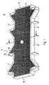
- FIG. 5 shows a specific embodiment of the light source element shown in FIG. This has a closed shape, wherein on its inner peripheral surface a plurality of successively arranged Lichteinkopplungsakuen 45 are provided (the light sources are not shown).
- the structure and structure of the optical waveguide 40 are as shown in FIG.
- the special form of the closed ring can be chosen arbitrarily.
- FIG. 6 shows an exemplary embodiment of a light source element 50 produced according to the invention, as can be used, for example, for backlighting a liquid crystal display in the dashboard of a motor vehicle.
- FIG. 7 shows the light source element in a cross section along the line II-II in FIG.
- the centerpiece of the light source element 50 of FIG. 6 is a planar optical waveguide 51, which in principle can be formed from any transparent material, for example from a thermoplastic resin such as acrylic resin, polycarbonate resin, or also from Plexiglas or PMMA (polymethyl methacrylate).
- a light source 55 such as a semiconductor light-emitting diode
- the optical waveguide 51 is surrounded on all sides by reflectors 54, through which the incident light radiation is reflected back diffusely.
- the end faces are also partially covered with reflectors 54 in an advantageous manner.
- openings 54A for the passage of the light radiation emitted by the light sources 55 are formed.
- the front surfaces are not covered by reflectors 54 from the outset.
- the optical waveguide 51 has a shape such that the plane of the light exit surface 51A forms an angle ⁇ with the plane of its opposite surface 51B. Therefore, when the optical fiber module in the illustrated form is mounted on a flat back wall, for example in the dashboard of a motor vehicle, the light exit surface 51A and thus also the liquid crystal element mounted in front of the light exit surface 51A are tilted and face an observer. Thus, it is achieved that the viewer looks at a mounted at a lower position of a dashboard liquid crystal display approximately perpendicular to the display surface, so that the visual defects occurring in the conventional optical fiber modules are avoided.
- the reflectors 54 are applied in the form of a foil material.
- This may for example be a film based on polycarbonate, which is coated or printed with white paint.
- the film could also be applied during the injection molding of the optical waveguide 50 by the shape of the injection molding apparatus is designed with the film before injection molding. After hardening of the plastic compound adheres the film on the waveguide and can be removed together with this from the injection molding apparatus.
- the homogenization of the luminance is in principle as well as in EP-A-0 500 960 brought about with a variable area ratio of light-scattering and flat surfaces which are formed on the light exit surface 51A and / or the opposite surface 51B of the optical waveguide 51 or both ,
- light-scattering surfaces 56 and planar surfaces 57 shaped by way of example only in the light exit surface 51A of the optical waveguide 51 are indicated.
- the area ratio of the flat surfaces 57 to the light-diffusing surfaces 56 depends on the luminance at the respective location in the optical waveguide 51. In areas of relatively high luminance in the optical waveguide 51, a relatively high area ratio is set, while this proportion is set low in areas of relatively low luminance.
- a particularly simple method of production is the generation of roughened areas by sanding the respective surface. At areas where the luminance is low, the surface is sandblasted to make the incident light scatter.
- the light-scattering regions 56 can also be, for example, small elevations which are applied in a targeted manner as a dot matrix on the surface.
- the density distribution in the dot matrix can be determined, for example, by a simulation program in which essentially the dimensions of the optical waveguide 51 and the locations and intensities of the light coupling as well as the reflection ratios are input.
- light sources are arranged at both end faces, of which light is coupled into the optical waveguide 51.
- FIG. 8 shows a perspective view of a further embodiment of a light source element 60 produced according to the invention, as can be used, for example, for backlighting a liquid crystal display.
- the core of the light source element 60 is a planar cuboid optical waveguide 61, which in principle is made of any transparent material, e.g. can be molded from a thermoplastic resin such as acrylic resin or polycarbonate resin. If the light source element according to the first embodiment of the invention is to be manufactured, the material must be an injection-moldable material.
- the light coupled into this optical waveguide 61 is homogeneously distributed over the rectangular area and fed to a (not shown) display surface of a liquid crystal display.
- a film 64 Through which the impinging surface 61B is applied Light radiation is reflected back into the optical waveguide 61 back diffuse.
- the light is coupled in by at least one light source 65, which are arranged in front of at least one of the end faces 61E or 61F of the light source element 60.
- the light source 65 is, for example, a semiconductor light emitting diode (LED) for monochrome backlighting of the liquid crystal display.
- miniaturized LEDs which can be mounted in SMT (surface mounted technique) and have become known, for example, under the trademarks SIDELED® and MiniSI-DELED®.
- SMT surface mounted technique
- MiniSI-DELED® MiniSI-DELED®.
- a very flat light source element light guide module
- a white light source such as a halogen lamp or the like can be used.
- the optical waveguide 61 is produced by injection molding, wherein the attachment of the film 64 takes place simultaneously.
- an injection molding apparatus is used which contains a shape which corresponds to the desired shape of the optical waveguide 61, that is in the embodiment has the shape of a flat cuboid.
- This shape ie substantially the bottom surface and the longitudinal side surfaces is designed with the film 64 prior to injection molding.
- the film can be pulled, for example as an endless film strip through the injection molding apparatus and sucked by vacuum into the mold. When closing the apparatus, the film is separated. Then, the injection molding is carried out with the plastic material. After curing of the plastic mass in the mold, the film 64 adheres to the optical waveguide 1 and this can be removed from the injection molding apparatus.
- the film 64 may be laid out on all side surfaces of the mold. In any case, it must be ensured that at the points where light sources 65 are arranged are either no film is provided or formed into an existing film openings of sufficient size in the film 64, through which the light radiation of the light sources 65 can enter into the optical waveguide 61.
- the film 64 is manufactured in a deep drawing process.
- the film 64 is integrally formed with the bottom surface and the side surfaces.
- the film may then be e.g. exist as a trough-shaped channel into which the optical waveguide 61 can be inserted.
- the film may consist essentially of a polycarbonate which is coated or printed with white paint. It may also consist of a multilayer structure of a polycarbonate layer, an aluminum layer and the white color layer.
- the homogenization of the luminance is in principle as well as in EP-A-0 500 960 brought about with a variable area ratio of light-scattering and flat surfaces which are formed on the light exit surface 61A and / or the opposite surface 61B of the optical waveguide 61 or both ,
- light-scattering surfaces 66 and planar surfaces 67 shaped merely by way of example into the light exit surface 61A of the optical waveguide 61 are indicated.
- the area ratio of the flat surfaces 67 to the light-diffusing surfaces 66 depends on the luminance at the respective location in the optical waveguide 61. In areas of relatively high luminance in the optical waveguide 61, a relatively high area ratio is set, while this proportion is set low in areas of relatively low luminance.
- the shape of the light-scattering surfaces 66 There are several possibilities for the shape of the light-scattering surfaces 66.
- a particularly simple method of production is the generation of roughened areas by sanding off the respective surface. In the places where a low luminance exists is, the surface is relatively intensively sanded to bring the incident light to the scattering.
- the light-scattering regions 66 can also be, for example, small elevations which are applied in a targeted manner as a dot matrix on the surface.
- the density distribution in the dot matrix can be determined, for example, by a simulation program in which essentially the dimensions of the optical waveguide 61 and the locations and intensities of the light coupling as well as the reflection ratios are input.
- a liquid crystal element above the light exit surface 61A is attached to the light source element by means of spacers.
- FIG. 10 is a perspective view of a partial view of another embodiment of a light source element 70 according to the invention.
- a light source 75 is arranged below the projection 71A so that the space above the light source 75 is additionally utilized by the projection 71A.
- the area of the light source element 70, and thus the usable display area of the liquid crystal display is increased.
- the surface of the projection 71A facing the light source 75 is also covered with the film 74.
- the mold of the injection molding apparatus must have a corresponding complementary shape for the further embodiment.
Claims (25)
- Élément source de lumière (10 ; 30) comprenant une fibre optique (1 ; 31), avec laquelle- il est prévu une surface de sortie de la lumière (1A ; 31A) et au moins une surface d'entrée de la lumière (5B ; 35B),- la surface (1B ; 51B) à l'opposé de la surface de sortie de la lumière (1A ; 31A) et au moins une partie des surfaces latérales (1C, 1D) qui relient la surface de sortie de la lumière (1A ; 31A) et la surface opposée étant recouvertes de réflecteurs (4, 34) réfléchissant la lumière ou la renvoyant de manière diffuse et- la surface d'entrée de la lumière (5B ; 35B) étant disposée selon un angle aigu par rapport à l'une des directions d'extension principale de la fibre optique,caractérisé en ce que- au moins l'un des réflecteurs recouvrant les surfaces latérales présente une zone d'ouverture et- la surface d'entrée de la lumière (5B ; 35B) est formée par cette partie non munie d'un réflecteur de la surface latérale (1C, 1D) correspondante.
- Élément source de lumière selon la revendication 1, caractérisé en ce que- une source de lumière (5A, 35A) est disposée sur la fibre optique avant la zone d'ouverture (5B) de telle sorte que- le rayonnement lumineux émis lors du fonctionnement de la source de lumière (5A) pénètre dans la fibre optique (1, 31) avec un angle oblique.
- Élément source de lumière selon la revendication 2, caractérisé en ce que- au moins une saillie triangulaire est façonnée dans au moins une surface latérale longitudinale (1C, 1D) ou la surface (1B) de la fibre optique (1, 31),- dont une surface latérale est recouverte par un réflecteur (4, 34) et- dont l'autre surface latérale est dégagée vers l'extérieur et forme ainsi la zone d'ouverture (5B, 35B).
- Élément source de lumière selon la revendication 1, caractérisé en ce que la fibre optique (51) présente une forme telle que la surface de sortie de la lumière (51A) et la surface (51B) de la fibre optique (51) qui lui est opposée forment un angle (α) différent de zéro.
- Élément source de lumière selon la revendication 2 ou 4, caractérisé en ce que- la surface de sortie de la lumière (1A ; 31A) et/ou la surface de la fibre optique qui lui est opposée présentent des sections diffusantes (6 ; 56 ; 66) et des sections planes (7 ; 57 ; 67),- et le rapport de surface entre les sections planes (7 ; 57 ; 67) et les sections diffusantes (6 ; 56 ; 66) le long de la fibre optique est réglé de manière à obtenir une densité lumineuse régulière de l'élément source de lumière.
- Élément source de lumière selon l'une des revendications précédentes, caractérisé en ce que les réflecteurs (4 ; 34) sont reliés entre eux d'une seule pièce.
- Élément source de lumière selon l'une des revendications précédentes, caractérisé en ce que le matériau des réflecteurs (4, 34) peut être moulé par injection et les réflecteurs (4, 34) sont fabriqués par moulage par injection.
- Élément source de lumière selon l'une des revendications 1 à 6, caractérisé en ce que le matériau des réflecteurs (4) est constitué d'un polyester thermoplastique, notamment à base de polybutènetéréphtalate.
- Élément source de lumière selon l'une des revendications 1 à 6, caractérisé en ce que le matériau des réflecteurs (4, 34) est du Pocan®.
- Élément source de lumière selon l'une des revendications 1 à 5, caractérisé en ce que les réflecteurs sont façonnés à partir d'un film (64, 74) réfléchissant ou renvoyant la lumière de manière diffuse.
- Élément source de lumière selon la revendication 10, caractérisé en ce que le film est façonné à base de polycarbonate.
- Élément source de lumière selon la revendication 10 ou 11, caractérisé en ce qu' éventuellement une ou plusieurs ouvertures sont façonnées dans le film (64, 74) pour le passage du rayonnement lumineux.
- Élément source de lumière selon l'une des revendications précédentes, caractérisé en ce que- la fibre optique (71) présente une partie en saillie (71A) dans l'alignement de la surface de sortie de la lumière (73) qui dépasse au-dessus d'une surface latérale,- sous laquelle est disposée l'au moins une source de lumière (75).
- Élément source de lumière selon la revendication 13, caractérisé en ce que la surface de la partie en saillie (71A) faisant face à la source de lumière (75) est également recouverte du film (74).
- Élément source de lumière selon l'une des revendications 10 à 14, caractérisé en ce que le film est revêtu ou imprimé avec de la couleur blanche.
- Élément source de lumière selon l'une des revendications précédentes, caractérisé en ce qu'il forme un anneau fermé.
- Élément source de lumière selon l'une ou plusieurs des revendications précédentes, caractérisé en ce que l'au moins une source de lumière est une diode électroluminescente en semiconducteur.
- Afficheur à cristaux liquides comprenant un élément source de lumière selon l'une ou plusieurs des revendications précédentes, caractérisé en ce qu'un élément à cristaux liquides est disposé sur le côté de la surface de sortie de la lumière.
- Afficheur à cristaux liquides selon la revendication 18, caractérisé en ce que l'élément à cristaux liquides est maintenu à une certaine distance de la surface de sortie de la lumière par des entretoises.
- Procédé de fabrication d'un élément source de lumière, caractérisé par les étapes- Fabrication d'une fibre optique par procédé de moulage par injection,- un moule prévu à cet effet d'un appareil de moulage par injection étant conçu avec un film réfléchissant la lumière ou la renvoyant de manière diffuse sur la surface de son fond et au moins une partie des surfaces latérales,- une matière plastique transparente étant injectée dans l'espace creux et- la fibre optique étant retirée après le durcissement,- Disposition d'au moins une source de lumière sur au moins une surface latérale de la fibre optique.
- Procédé selon la revendication 20, caractérisé en ce que- le film est dimensionné sur toutes les surfaces latérales dans le moule de l'appareil de moulage par injection et- des ouvertures correspondantes sont aménagées dans le film pour le passage du rayonnement lumineux avant la pose de l'au moins une source de lumière.
- Procédé de fabrication d'un élément source de lumière, caractérisé par les étapes- Fabrication d'une fibre optique,- Fabrication d'un film réfléchissant la lumière ou la renvoyant de manière diffuse, lequel présente une surface de fond et au moins une surface latérale, par un procédé d'emboutissage,- Application du film sur la fibre optique,- Disposition d'au moins une source de lumière sur au moins une surface latérale de la fibre optique.
- Procédé selon la revendication 22, caractérisé en ce que des ouvertures correspondantes sont aménagées dans le film pour le passage du rayonnement lumineux avant la pose de l'au moins une source de lumière.
- Procédé selon l'une des revendications 20 à 23, caractérisé en ce que le film est revêtu ou imprimé avec de la couleur blanche.
- Procédé selon l'une des revendications 20 à 24, caractérisé en ce que le film contient du polycarbonate.
Applications Claiming Priority (7)
| Application Number | Priority Date | Filing Date | Title |
|---|---|---|---|
| DE1998160695 DE19860695B4 (de) | 1998-12-29 | 1998-12-29 | Lichtquellenelement mit schräggestellter Lichtaustrittsfläche |
| DE19860697 | 1998-12-29 | ||
| DE1998160696 DE19860696B4 (de) | 1998-12-29 | 1998-12-29 | Lichtquellenelement mit seitlicher schräger Lichteinkopplung |
| DE1998160697 DE19860697A1 (de) | 1998-12-29 | 1998-12-29 | Verfahren zur Herstellung eines flachen Lichtleitermoduls |
| DE19860696 | 1998-12-29 | ||
| DE19860695 | 1998-12-29 | ||
| PCT/DE1999/004125 WO2000039501A1 (fr) | 1998-12-29 | 1999-12-29 | Source lumineuse a couplage lateral oblique de lumiere |
Publications (2)
| Publication Number | Publication Date |
|---|---|
| EP1141623A1 EP1141623A1 (fr) | 2001-10-10 |
| EP1141623B1 true EP1141623B1 (fr) | 2006-09-27 |
Family
ID=27218905
Family Applications (1)
| Application Number | Title | Priority Date | Filing Date |
|---|---|---|---|
| EP99966896A Expired - Lifetime EP1141623B1 (fr) | 1998-12-29 | 1999-12-29 | Source lumineuse a couplage lateral oblique de lumiere |
Country Status (9)
| Country | Link |
|---|---|
| US (2) | US7688400B1 (fr) |
| EP (1) | EP1141623B1 (fr) |
| JP (1) | JP2002533892A (fr) |
| KR (1) | KR100402718B1 (fr) |
| CN (1) | CN1120327C (fr) |
| AT (1) | ATE340967T1 (fr) |
| DE (1) | DE59913882D1 (fr) |
| TW (1) | TW454100B (fr) |
| WO (1) | WO2000039501A1 (fr) |
Families Citing this family (21)
| Publication number | Priority date | Publication date | Assignee | Title |
|---|---|---|---|---|
| DE10229064B4 (de) * | 2002-06-28 | 2008-08-14 | Osram Gesellschaft mit beschränkter Haftung | Flüssigkristall-Display |
| JP2004355889A (ja) * | 2003-05-28 | 2004-12-16 | Mitsubishi Electric Corp | 平面光源装置及び表示装置 |
| DE102004046256A1 (de) * | 2004-09-23 | 2006-04-06 | Osram Opto Semiconductors Gmbh | Oberflächenleuchtsystem |
| NL1030161C2 (nl) | 2005-10-11 | 2007-04-12 | Matthijs Dirk Meulenbelt | Presentatie-inrichting. |
| WO2009040725A2 (fr) * | 2007-09-26 | 2009-04-02 | Koninklijke Philips Electronics N. V. | Lampe à laser |
| KR20100135295A (ko) * | 2008-04-17 | 2010-12-24 | 스미토모덴키고교가부시키가이샤 | 배광 제어 패널, 이동체 탑재용 표시 장치, 배광 제어 시트, 광학 부품, 조명 장치 및 표시 장치 |
| JP5169594B2 (ja) * | 2008-08-01 | 2013-03-27 | セイコーエプソン株式会社 | 照明装置、および液晶表示装置 |
| CN102203500B (zh) * | 2008-11-17 | 2013-12-25 | 阿尔卑斯电气株式会社 | 照明装置以及用于其中的导光板的制造方法 |
| EP2408867A4 (fr) * | 2009-03-20 | 2013-03-06 | Eric William Hearn Teather | Composition de peinture réfléchissant la lumière par diffusion, procédé pour préparer la composition de peinture et articles réfléchissant la lumière par diffusion |
| US8361611B2 (en) * | 2009-03-20 | 2013-01-29 | Whiteoptics Llc | Diffusively light reflective paint composition, method for making paint composition, and diffusively light reflective articles |
| US20100238665A1 (en) * | 2009-03-20 | 2010-09-23 | Eric William Hearn Teather | Diffusive light reflectors with polymeric coating |
| US20110219648A1 (en) * | 2010-03-12 | 2011-09-15 | Trevor James | Led edge-lit signage utilizing digital print technology |
| EP2583126B1 (fr) * | 2010-06-17 | 2020-08-05 | Signify Holding B.V. | Dispositif d'éclairage ayant un guide d'ondes et des diodes électroluminescentes |
| WO2012166103A1 (fr) * | 2011-05-27 | 2012-12-06 | Empire Technology Development Llc | Éclairage utilisant la lumière naturelle |
| WO2013019023A2 (fr) * | 2011-07-29 | 2013-02-07 | Lg Innotek Co., Ltd. | Dispositif d'éclairage et dispositif d'affichage à cristaux liquides comprenant ce dernier |
| DE102012203293B4 (de) * | 2012-03-02 | 2021-12-02 | Robert Bosch Gmbh | Halbleitermodul mit integriertem Wellenleiter für Radarsignale |
| US9772439B2 (en) * | 2016-02-05 | 2017-09-26 | Sharp Kabushiki Kaisha | Thin backlight with reduced bezel width |
| US20180188685A1 (en) * | 2016-12-30 | 2018-07-05 | Luminit, Llc | Monolithic Optical System for Light Propagation in Confined Spaces and Method of Fabrication |
| WO2019092824A1 (fr) * | 2017-11-09 | 2019-05-16 | Necディスプレイソリューションズ株式会社 | Corps de conduit de lumière, unité de corps de conduit de lumière et procédé de fabrication associé, et équipement électronique |
| US10914431B2 (en) * | 2017-12-31 | 2021-02-09 | Google Llc | Smart-home device light rings with tapered transmissive sections for uniform output |
| DE102018215988A1 (de) | 2018-09-19 | 2020-03-19 | Volkswagen Aktiengesellschaft | Lichtmodul, insbesondere zur Verwendung in einer Beleuchtungsvorrichtung für ein Kraftfahrzeug |
Family Cites Families (25)
| Publication number | Priority date | Publication date | Assignee | Title |
|---|---|---|---|---|
| US4059916A (en) * | 1975-01-30 | 1977-11-29 | Copal Company Limited | Light diffusing device |
| DE2827573C2 (de) * | 1978-06-23 | 1983-02-03 | Blaupunkt-Werke Gmbh, 3200 Hildesheim | Großflächige Lichtquelle |
| GB8816952D0 (en) * | 1988-07-15 | 1988-08-17 | Emi Plc Thorn | Display device |
| US5667289A (en) * | 1989-05-18 | 1997-09-16 | Seiko Epson Corporation | Background lighting apparatus for liquid crystal display |
| EP1022787B2 (fr) * | 1989-05-31 | 2012-07-11 | OSRAM Opto Semiconductors GmbH | Procédé de production d'un élément optique fixable sur une surface et élément optique fixable sur une surface |
| CA2068422A1 (fr) | 1990-09-12 | 1992-03-13 | Makoto Ohe | Source lumineuse pour dispositif d'affichage plat |
| JP3025080B2 (ja) | 1991-11-21 | 2000-03-27 | 株式会社シマノ | 釣り用リール |
| US5211463A (en) * | 1992-03-11 | 1993-05-18 | Kaiser Aerospace & Electronics Corporation | Backlight for liquid crystal devices |
| DE69333439T2 (de) | 1992-07-13 | 2005-02-10 | Seiko Epson Corp. | Flächenhafte Beleuchtungsvorrichtung und Flüssigkristallanzeige |
| US5339179A (en) * | 1992-10-01 | 1994-08-16 | International Business Machines Corp. | Edge-lit transflective non-emissive display with angled interface means on both sides of light conducting panel |
| JPH0721817A (ja) | 1993-06-30 | 1995-01-24 | Toshiba Lighting & Technol Corp | 照明装置,バックライトおよび液晶表示装置 |
| DE4404425A1 (de) | 1994-02-11 | 1995-08-17 | Rudolf Goeckel | Vorrichtung zur diffusen Ausleuchtung transparenter Flächen oder Körper |
| US5671994A (en) * | 1994-06-08 | 1997-09-30 | Clio Technologies, Inc. | Flat and transparent front-lighting system using microprisms |
| JPH08106011A (ja) | 1994-10-03 | 1996-04-23 | Ohtsu Tire & Rubber Co Ltd :The | 導光板、その光乱反射部用転写シート及びその光乱反射部の形成方法 |
| JPH08248420A (ja) * | 1995-03-07 | 1996-09-27 | Casio Comput Co Ltd | 液晶表示装置 |
| GB2301894B (en) * | 1995-06-07 | 1998-03-11 | Toyoda Gosei Kk | Light-driven display device |
| JPH09113907A (ja) | 1995-10-17 | 1997-05-02 | Nippon Chemitec Kk | 導光板と該導光板を使用した面型照明体 |
| JP3330489B2 (ja) * | 1996-04-05 | 2002-09-30 | 松下電器産業株式会社 | 液晶用バックライト |
| DE19652829B4 (de) | 1996-04-19 | 2008-04-30 | BSH Bosch und Siemens Hausgeräte GmbH | Wasserkocher mit Betriebsanzeige |
| JP3231655B2 (ja) * | 1997-03-28 | 2001-11-26 | シャープ株式会社 | 前方照明装置およびこれを備えた反射型液晶表示装置 |
| US6369867B1 (en) * | 1998-03-12 | 2002-04-09 | Gl Displays, Inc. | Riveted liquid crystal display comprising at least one plastic rivet formed by laser drilling through a pair of plastic plates |
| US6447134B1 (en) * | 1998-05-11 | 2002-09-10 | Toyoda Gosei Co., Ltd. | Planar light emitting device |
| US6297908B1 (en) * | 1998-06-05 | 2001-10-02 | Dai Nippon Printing Co., Ltd. | Directional light-diffusing film, a method of manufacturing same, and a display device that uses same |
| US6439731B1 (en) * | 1999-04-05 | 2002-08-27 | Honeywell International, Inc. | Flat panel liquid crystal display |
| US6356389B1 (en) * | 1999-11-12 | 2002-03-12 | Reflexite Corporation | Subwavelength optical microstructure light collimating films |
-
1999
- 1999-12-29 JP JP2000591363A patent/JP2002533892A/ja active Pending
- 1999-12-29 TW TW088123204A patent/TW454100B/zh not_active IP Right Cessation
- 1999-12-29 AT AT99966896T patent/ATE340967T1/de not_active IP Right Cessation
- 1999-12-29 US US09/868,364 patent/US7688400B1/en not_active Expired - Fee Related
- 1999-12-29 CN CN99815213A patent/CN1120327C/zh not_active Expired - Lifetime
- 1999-12-29 WO PCT/DE1999/004125 patent/WO2000039501A1/fr active IP Right Grant
- 1999-12-29 DE DE59913882T patent/DE59913882D1/de not_active Expired - Lifetime
- 1999-12-29 KR KR10-2001-7008367A patent/KR100402718B1/ko active IP Right Grant
- 1999-12-29 EP EP99966896A patent/EP1141623B1/fr not_active Expired - Lifetime
-
2007
- 2007-05-14 US US11/748,058 patent/US7688401B2/en not_active Expired - Fee Related
Also Published As
| Publication number | Publication date |
|---|---|
| TW454100B (en) | 2001-09-11 |
| US20070263411A1 (en) | 2007-11-15 |
| KR20010086467A (ko) | 2001-09-12 |
| US7688400B1 (en) | 2010-03-30 |
| WO2000039501A1 (fr) | 2000-07-06 |
| DE59913882D1 (de) | 2006-11-09 |
| ATE340967T1 (de) | 2006-10-15 |
| CN1332835A (zh) | 2002-01-23 |
| JP2002533892A (ja) | 2002-10-08 |
| CN1120327C (zh) | 2003-09-03 |
| US7688401B2 (en) | 2010-03-30 |
| EP1141623A1 (fr) | 2001-10-10 |
| KR100402718B1 (ko) | 2003-10-22 |
Similar Documents
| Publication | Publication Date | Title |
|---|---|---|
| EP1141623B1 (fr) | Source lumineuse a couplage lateral oblique de lumiere | |
| DE60221434T2 (de) | Lichtleiterleuchte geeignet für beleuchtete anzeigevorrichtungen | |
| DE102016110054B4 (de) | Beleuchtungseinrichtung und Interieurteil für ein Fahrzeug | |
| EP2354637B1 (fr) | Dispositif d'éclairage pour véhicules | |
| DE10258465B4 (de) | Beleuchtungsvorrichtung für ein Kennzeichenschild | |
| DE10123263B4 (de) | Lichtleitsystem für den Innenraum eines Kraftfahrzeugs | |
| EP1387982B1 (fr) | Element optique a reflexion totale | |
| DE112017004923B4 (de) | Lichtführungselement, Lichtführungseinheit und Beleuchtungsvorrichtung | |
| DE202020005400U1 (de) | Linienleuchte | |
| AT518118B1 (de) | Beleuchtungseinheit für ein Kraftfahrzeug | |
| DE102004054732B4 (de) | Lichtleiteranordung | |
| DE102005017639B4 (de) | Lichtleiteranordnung sowie Verfahren zur Herstellung einer solchen | |
| WO2000011399A1 (fr) | Lampe dotee d'un guide de lumiere | |
| EP3071879B1 (fr) | Élément optique et dispositif d'éclairage doté d'un élément optique | |
| EP3655289A1 (fr) | Composant pour un véhicule | |
| DE19860697A1 (de) | Verfahren zur Herstellung eines flachen Lichtleitermoduls | |
| DE102013007856A1 (de) | Lichtleitkörper und Leuchtvorrichtung mit dem Lichtleitkörper | |
| DE19860696B4 (de) | Lichtquellenelement mit seitlicher schräger Lichteinkopplung | |
| DE102016116146A1 (de) | Bandförmige, flächige Leuchtvorrichtung für ein Kraftfahrzeug | |
| DE102009007198A1 (de) | Fahrzeug mit Armaturenbrett und Anzeigevorrichtung für das Armaturenbrett sowie ein Verfahren zur Herstellung der Anzeigevorrichtung | |
| DE102020132976A1 (de) | Lichtleiter für leuchten und zugehörige leuchten für kraftfahrzeuge | |
| DE10037642A1 (de) | Leuchtfläche | |
| DE102011000702A1 (de) | Rollfeldverkehrszeichen | |
| DE19860695B4 (de) | Lichtquellenelement mit schräggestellter Lichtaustrittsfläche | |
| DE102017122429A1 (de) | Formteil, insbesondere als Formteil ausgebildetes Dekorteil und/oder Verkleidungsteil für einen Fahrzeuginnenraum und ein Verfahren zum Herstellen eines solchen Formteils |
Legal Events
| Date | Code | Title | Description |
|---|---|---|---|
| PUAI | Public reference made under article 153(3) epc to a published international application that has entered the european phase |
Free format text: ORIGINAL CODE: 0009012 |
|
| 17P | Request for examination filed |
Effective date: 20010601 |
|
| AK | Designated contracting states |
Kind code of ref document: A1 Designated state(s): AT BE CH CY DE DK ES FI FR GB GR IE IT LI LU MC NL PT SE |
|
| 17Q | First examination report despatched |
Effective date: 20020730 |
|
| GRAP | Despatch of communication of intention to grant a patent |
Free format text: ORIGINAL CODE: EPIDOSNIGR1 |
|
| GRAS | Grant fee paid |
Free format text: ORIGINAL CODE: EPIDOSNIGR3 |
|
| GRAA | (expected) grant |
Free format text: ORIGINAL CODE: 0009210 |
|
| AK | Designated contracting states |
Kind code of ref document: B1 Designated state(s): AT BE CH CY DE DK ES FI FR GB GR IE IT LI LU MC NL PT SE |
|
| PG25 | Lapsed in a contracting state [announced via postgrant information from national office to epo] |
Ref country code: NL Free format text: LAPSE BECAUSE OF FAILURE TO SUBMIT A TRANSLATION OF THE DESCRIPTION OR TO PAY THE FEE WITHIN THE PRESCRIBED TIME-LIMIT Effective date: 20060927 Ref country code: IT Free format text: LAPSE BECAUSE OF FAILURE TO SUBMIT A TRANSLATION OF THE DESCRIPTION OR TO PAY THE FEE WITHIN THE PRESCRIBED TIME-LIMIT;WARNING: LAPSES OF ITALIAN PATENTS WITH EFFECTIVE DATE BEFORE 2007 MAY HAVE OCCURRED AT ANY TIME BEFORE 2007. THE CORRECT EFFECTIVE DATE MAY BE DIFFERENT FROM THE ONE RECORDED. Effective date: 20060927 Ref country code: IE Free format text: LAPSE BECAUSE OF FAILURE TO SUBMIT A TRANSLATION OF THE DESCRIPTION OR TO PAY THE FEE WITHIN THE PRESCRIBED TIME-LIMIT Effective date: 20060927 Ref country code: FI Free format text: LAPSE BECAUSE OF FAILURE TO SUBMIT A TRANSLATION OF THE DESCRIPTION OR TO PAY THE FEE WITHIN THE PRESCRIBED TIME-LIMIT Effective date: 20060927 |
|
| REG | Reference to a national code |
Ref country code: GB Ref legal event code: FG4D Free format text: NOT ENGLISH |
|
| REG | Reference to a national code |
Ref country code: CH Ref legal event code: EP |
|
| REG | Reference to a national code |
Ref country code: IE Ref legal event code: FG4D Free format text: LANGUAGE OF EP DOCUMENT: GERMAN |
|
| REF | Corresponds to: |
Ref document number: 59913882 Country of ref document: DE Date of ref document: 20061109 Kind code of ref document: P |
|
| PG25 | Lapsed in a contracting state [announced via postgrant information from national office to epo] |
Ref country code: SE Free format text: LAPSE BECAUSE OF FAILURE TO SUBMIT A TRANSLATION OF THE DESCRIPTION OR TO PAY THE FEE WITHIN THE PRESCRIBED TIME-LIMIT Effective date: 20061227 Ref country code: DK Free format text: LAPSE BECAUSE OF FAILURE TO SUBMIT A TRANSLATION OF THE DESCRIPTION OR TO PAY THE FEE WITHIN THE PRESCRIBED TIME-LIMIT Effective date: 20061227 |
|
| PG25 | Lapsed in a contracting state [announced via postgrant information from national office to epo] |
Ref country code: MC Free format text: LAPSE BECAUSE OF NON-PAYMENT OF DUE FEES Effective date: 20061231 Ref country code: LI Free format text: LAPSE BECAUSE OF NON-PAYMENT OF DUE FEES Effective date: 20061231 Ref country code: CH Free format text: LAPSE BECAUSE OF NON-PAYMENT OF DUE FEES Effective date: 20061231 Ref country code: BE Free format text: LAPSE BECAUSE OF NON-PAYMENT OF DUE FEES Effective date: 20061231 |
|
| PG25 | Lapsed in a contracting state [announced via postgrant information from national office to epo] |
Ref country code: ES Free format text: LAPSE BECAUSE OF FAILURE TO SUBMIT A TRANSLATION OF THE DESCRIPTION OR TO PAY THE FEE WITHIN THE PRESCRIBED TIME-LIMIT Effective date: 20070107 |
|
| NLV1 | Nl: lapsed or annulled due to failure to fulfill the requirements of art. 29p and 29m of the patents act | ||
| PG25 | Lapsed in a contracting state [announced via postgrant information from national office to epo] |
Ref country code: PT Free format text: LAPSE BECAUSE OF FAILURE TO SUBMIT A TRANSLATION OF THE DESCRIPTION OR TO PAY THE FEE WITHIN THE PRESCRIBED TIME-LIMIT Effective date: 20070313 |
|
| REG | Reference to a national code |
Ref country code: IE Ref legal event code: FD4D |
|
| GBV | Gb: ep patent (uk) treated as always having been void in accordance with gb section 77(7)/1977 [no translation filed] |
Effective date: 20060927 |
|
| EN | Fr: translation not filed | ||
| REG | Reference to a national code |
Ref country code: CH Ref legal event code: PL |
|
| PLBE | No opposition filed within time limit |
Free format text: ORIGINAL CODE: 0009261 |
|
| STAA | Information on the status of an ep patent application or granted ep patent |
Free format text: STATUS: NO OPPOSITION FILED WITHIN TIME LIMIT |
|
| 26N | No opposition filed |
Effective date: 20070628 |
|
| PG25 | Lapsed in a contracting state [announced via postgrant information from national office to epo] |
Ref country code: GB Free format text: LAPSE BECAUSE OF FAILURE TO SUBMIT A TRANSLATION OF THE DESCRIPTION OR TO PAY THE FEE WITHIN THE PRESCRIBED TIME-LIMIT Effective date: 20060927 |
|
| BERE | Be: lapsed |
Owner name: OSRAM OPTO SEMICONDUCTORS G.M.B.H. & CO. OHG Effective date: 20061231 |
|
| PG25 | Lapsed in a contracting state [announced via postgrant information from national office to epo] |
Ref country code: AT Free format text: LAPSE BECAUSE OF NON-PAYMENT OF DUE FEES Effective date: 20061229 |
|
| PG25 | Lapsed in a contracting state [announced via postgrant information from national office to epo] |
Ref country code: GR Free format text: LAPSE BECAUSE OF FAILURE TO SUBMIT A TRANSLATION OF THE DESCRIPTION OR TO PAY THE FEE WITHIN THE PRESCRIBED TIME-LIMIT Effective date: 20061228 Ref country code: FR Free format text: LAPSE BECAUSE OF FAILURE TO SUBMIT A TRANSLATION OF THE DESCRIPTION OR TO PAY THE FEE WITHIN THE PRESCRIBED TIME-LIMIT Effective date: 20070525 |
|
| PG25 | Lapsed in a contracting state [announced via postgrant information from national office to epo] |
Ref country code: LU Free format text: LAPSE BECAUSE OF NON-PAYMENT OF DUE FEES Effective date: 20061229 |
|
| PG25 | Lapsed in a contracting state [announced via postgrant information from national office to epo] |
Ref country code: FR Free format text: LAPSE BECAUSE OF FAILURE TO SUBMIT A TRANSLATION OF THE DESCRIPTION OR TO PAY THE FEE WITHIN THE PRESCRIBED TIME-LIMIT Effective date: 20060927 Ref country code: CY Free format text: LAPSE BECAUSE OF FAILURE TO SUBMIT A TRANSLATION OF THE DESCRIPTION OR TO PAY THE FEE WITHIN THE PRESCRIBED TIME-LIMIT Effective date: 20060927 |
|
| PGFP | Annual fee paid to national office [announced via postgrant information from national office to epo] |
Ref country code: DE Payment date: 20181210 Year of fee payment: 20 |
|
| REG | Reference to a national code |
Ref country code: DE Ref legal event code: R071 Ref document number: 59913882 Country of ref document: DE |