EP1136834A2 - Circuit intégré comprenant un circuit de commande pour commander un circuit d'attaque - Google Patents
Circuit intégré comprenant un circuit de commande pour commander un circuit d'attaque Download PDFInfo
- Publication number
- EP1136834A2 EP1136834A2 EP01104729A EP01104729A EP1136834A2 EP 1136834 A2 EP1136834 A2 EP 1136834A2 EP 01104729 A EP01104729 A EP 01104729A EP 01104729 A EP01104729 A EP 01104729A EP 1136834 A2 EP1136834 A2 EP 1136834A2
- Authority
- EP
- European Patent Office
- Prior art keywords
- signal
- input
- output
- comparison device
- circuit
- Prior art date
- Legal status (The legal status is an assumption and is not a legal conclusion. Google has not performed a legal analysis and makes no representation as to the accuracy of the status listed.)
- Withdrawn
Links
Images
Classifications
-
- G—PHYSICS
- G01—MEASURING; TESTING
- G01R—MEASURING ELECTRIC VARIABLES; MEASURING MAGNETIC VARIABLES
- G01R31/00—Arrangements for testing electric properties; Arrangements for locating electric faults; Arrangements for electrical testing characterised by what is being tested not provided for elsewhere
- G01R31/28—Testing of electronic circuits, e.g. by signal tracer
- G01R31/317—Testing of digital circuits
- G01R31/3181—Functional testing
- G01R31/3185—Reconfiguring for testing, e.g. LSSD, partitioning
-
- G—PHYSICS
- G01—MEASURING; TESTING
- G01R—MEASURING ELECTRIC VARIABLES; MEASURING MAGNETIC VARIABLES
- G01R31/00—Arrangements for testing electric properties; Arrangements for locating electric faults; Arrangements for electrical testing characterised by what is being tested not provided for elsewhere
- G01R31/28—Testing of electronic circuits, e.g. by signal tracer
- G01R31/317—Testing of digital circuits
- G01R31/31712—Input or output aspects
- G01R31/31715—Testing of input or output circuits; test of circuitry between the I/C pins and the functional core, e.g. testing of input or output driver, receiver, buffer
Definitions
- the present invention relates to an integrated circuit with a connection for a digital signal, with a controllable Driver circuit, which has an input with the connector for the digital signal is connected, and one Output for outputting the digital signal, and with a control circuit, which is an input for a clock signal has to control the driver circuit in dependence of the clock signal.
- a digital signal In the operation of integrated circuits, it is often necessary generate or adjust a digital signal so that the timing of a switching edge of the digital signal at a point in time of a switching edge of a clock signal is adjusted.
- the frequency of that from the oscillator circuit generated signal is to be set so that they are with the frequency of the clock signal as the reference frequency matches, especially so precisely that an existing one Phase shift remains the same.
- An integrated circuit has one for this purpose Connection for the digital signal, for example, a controllable Driver circuit on that with the connector for the digital Signal is connected, and which is used to output the digital Signal is used.
- the driver circuit is activated by a control circuit driven which is an input for a Has clock signal.
- the drive circuit is, for example, in a certain Range adjustable based on a reference value, in particular Influences of process fluctuations and temperature fluctuations to be able to compensate. That means on the train the manufacture of such integrated circuits the respective reference values separately for each of the integrated circuits set and thus adjusted. For this purpose, the reference value is changed in a suitable manner, that the different influences are compensated.
- the control circuit is based on the reference value trimmed so that the required signal synchronization is set.
- the integrated Circuit that, for example, part of an integrated Storage is subjected to a test in this regard.
- This test is carried out, for example, externally using one for this provided test system performed.
- specifications for setting the control circuit Are defined.
- the switching edges of the corresponding digital signal and the clock signal with each other compared and by setting the drive circuit timed.
- the achievable accuracy will generally limited by tolerances of the used Test system and the entire test arrangement. This can lead to Consequence that a required product specification of the integrated circuit and thus the integrated memory is not fulfilled.
- the object of the present invention is an integrated Specify circuit of the type mentioned at the beginning a time comparison of switching edges in a test operation of the clock signal and the digital signal at the output the controllable driver circuit with a comparatively high accuracy is feasible.
- the task is solved by an integrated circuit with a connection for a digital signal, with a controllable Driver circuit which has an input which is connected to the Connection for the digital signal is connected, and the one Output has to output the digital signal, and with a drive circuit that has an input for a clock signal has to control the driver circuit in dependence the clock signal; where the integrated circuit a comparison device having a first input for the clock signal and a second input which is connected to the output of the driver circuit, and the has an output for outputting an output signal; at the output signal of the comparison device is a first Has state when a signal transition of the signal on the first Input before a signal transition of the signal on the second Input occurs; and in which the output signal of the comparison device has a second state when the Signal transition of the signal at the first input after the signal transition of the signal at the second input.
- a temporal comparison of the signal transitions or switching edges the digital signal at the output of the driver circuit and of the clock signal is carried out by the comparison device, the Is part of the integrated circuit.
- the output signal the comparison device shows which of the Signals at the inputs of the comparison device first one Has signal transition.
- the output signal of the comparison device is, for example, a connection for an external analysis facility. There the state becomes a taken output signal of the comparison device analyzed, whereupon a setting of the drive circuit based on the analysis result in the required manner can be done.
- the corresponding signal transitions not measured directly by an external test system and being analyzed will be more accurate the measurement reached. Since the measurement is made directly on the chip integrated circuit, the measurement accuracy is not through the tolerance of an external test system and the whole Test setup limited.
- a corresponding state of the output signal of the comparison device is advantageously in the comparison device saved. This allows the output signal the comparison device for a longer period of time for example by the external analysis device be removed.
- the output signal of the comparison device also has a static state, so that interference not essential when taking the output signal lead to a falsification of the comparison result.
- the control function of the control circuit is, for example adjustable based on a reference value.
- the control circuit In order to the reference value only needs to be set once it is advantageous that the reference value in a storage unit the control circuit is stored.
- the storage unit then has, for example, programmable elements in Form of laser fuses or electrically programmable fuses on.
- the laser fuses are used to set the reference value programmed by a so-called laser cutter.
- the integrated circuit is, for example, part of a integrated memory, for example a so-called SDRAMs (Synchronous DRAM).
- SDRAMs Synchronous DRAM
- DDR SDRAM Double Data Rate SDRAMs
- memories usually have which is usually supplied externally, a data validity signal or data clock signal ("data strobe"), which is connected to an external connection, for example to Reading data from the integrated memory.
- data strobe data validity signal
- This data strobe signal is read together with data signals to be output from the integrated memory transmitted externally.
- the switching edges of the data strobe signal are by means of a So-called DLL circuit ("Delay-Locked-Loop") with the Switching edges of the clock signal synchronized.
- the data strobe signal has a switching edge at the same time with the clock signal.
- the DLL circuit serves as a control circuit for a driver circuit that has the data strobe signal outputs that, for example, by an oscillator circuit is generated and at the input of the driver circuit is present.
- a kind of internal Clock signal generated from the external clock signal that at the Driver circuit is present. So there is a certain phase shift the internal clock signal or the data strobe signal adjustable compared to the externally supplied clock signal.
- the comparison device In one embodiment of the invention is the first input the comparison device with a first setting input Toggle switch and the second input of the comparison device connected to a second set input of the multivibrator.
- the output of the comparison device is with an output the flip-flop connected.
- the output signal of the Toggle switch shows which of the signals to the Set inputs first have a signal transition.
- the integrated Circuit a functional unit on that with the output of the Comparison device and connected to the control circuit is.
- the functional unit is used to set the Control circuit based on the state of the output signal the comparison device. This enables the control circuit for example by means of electrical signals adjust. Since the functional unit is part of the integrated Circuit, no external connections need to be made integrated circuit can be provided to an electrical Perform setting of the control circuit. Moreover shorter test times can be achieved because there are several circuits can be trimmed in parallel.
- the functional unit can, for example, electrically programmable fuses are contained in the control circuit, programmed become.
- the functional unit a self-test unit, with the successive one States of the output signal of the comparison device can be analyzed.
- the self-test unit serves also for the gradual setting of the control circuit based on an analysis result. By means of the self-test unit is therefore a completely independent trim Control circuit possible.
- the self-test unit is included realized according to the principle of the "Built-In-Self-Test" (BIST).
- BIST Battery-In-Self-Test
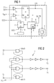
- FIG. 1 shows an embodiment of the integrated according to the invention Circuit arranged on a semiconductor chip 1 is.
- the integrated circuit is in a memory circuit of type DRAM included, for example in a DDR SDRAM.
- the integrated memory has a clock signal CK or a complementary clock signal CK on a external connection is supplied.
- the memory also points a so-called data strobe signal DQS, which via a external connection together with data signals to be output of the memory is transferred externally.
- the data strobe signal DQS acts as a data validity signal or data clock signal of the memory for reading out data of memory.
- the integrated circuit also has a drive circuit 3, which is referred to as a DLL circuit.
- the connection 10 for the signal DQS is connected to an oscillator circuit 9.
- the control circuit 3 has an input 31 for the clock signal CK or CK ,
- the control circuit 3 serves to control a controllable driver circuit 2 which has an input 21 which is connected to a connection 10 for the signal DQS and an output 22 for outputting the signal DQS.
- the control circuit 3 generates a type of internal clock signal from the external clock signal CK or CK with a certain phase shift compared to this.
- the driver circuit 2 is thus driven by the internal clock signal.
- signal transitions of the signal DQS are coordinated with signal transitions of the clock signal CK or CK, or the signal transitions are synchronized with one another. There is a certain phase shift of the signal DQS with respect to the externally supplied clock signal CK or CK adjustable. During a read access, the signal DQS is transmitted from the integrated memory to the outside together with data signals to be output.
- the integrated circuit according to FIG. 1 also has a comparison device 4 which has a first input 41 for the clock signal CK or CK and has a second input 42 which is connected to the output 22 of the driver circuit 2.
- An output 43 of the comparison device 4 is used to output an output signal A.
- the output signal A has a first state "H” when a signal transition of the signal at the input 41 occurs before a signal transition of the signal at the input 42. Accordingly, the output signal A has a second state "L” when the signal transition of the signal at input 41 occurs after the signal transition of the signal at input 42.
- the comparison device 4 has a further output 44, which has a signal which indicates the reverse order of the signal transitions via corresponding states. Resetting the comparison device 4 is possible with a corresponding signal at a connection 45.
- the clock signal CK or CK is connected to the input 41 of the comparison device 4 via a differential amplifier 11.
- the signal DQS is also connected to the input 42 of the comparison device 4 via a differential amplifier 12, to which a reference potential V ref is present.
- the integrated circuit also has a functional unit 5 on that with the output 43 of the comparison device 4 and is connected to the control circuit 3.
- the Functional unit 5 is used to set the control circuit 3 based on the state of the output signal A Comparison device 4.
- the functional unit 5 is a Setting the control circuit 3 by means of a electrical signal possible.
- control circuit 3 In the control circuit 3 is a reference value in one Storage unit 8 stored.
- the control function of the control circuit 3 is based on the stored reference value adjustable.
- the memory unit 8 has programmable Elements F in the form of programmable fuses. If a programming of the memory unit 8 by the Functional unit 5 performed, so are the programmable Fuses F in a suitable manner as electrically programmable Fuses executed.
- the Functional unit 5 a self-test unit 6 for analysis of successive states of the output signal A of the comparison device 4.
- the self-test unit 6 is an independent trimming of the drive circuit 3 possible.
- the comparison result is no longer necessary via an external connection or the setting of the control circuit 3 via external connection.
- the self test unit 6 is suitable, a gradual setting of the control circuit 3 based on an analysis result.
- FIG. 2 shows an embodiment of the comparison device 4 shown.
- This has a flip-flop 7 with a first set input 71 and a second set input 72.
- the Set input 71 is connected to input 41 of the comparison device 4, the set input 72 is connected to the input 42 the comparison device 4 connected.
- the flip-flop 7 has an output 73 which is connected to the output 43 of the comparison device 4 is connected. The further exit 44 the comparison device 4 is with an output 74 Toggle switch 7 connected.
- a toggle reset input 75 7 is with the terminal 45 of the comparison device 4 connected.
- the output signal at output 73 of the flip-flop 7 shows which of the signals at the set inputs 71 or 72 first has a signal transition. Until reset the flip-flop 7 is the respective output signal saved at output 73.
Landscapes
- Engineering & Computer Science (AREA)
- General Engineering & Computer Science (AREA)
- Physics & Mathematics (AREA)
- General Physics & Mathematics (AREA)
- Dram (AREA)
- Tests Of Electronic Circuits (AREA)
- For Increasing The Reliability Of Semiconductor Memories (AREA)
- Logic Circuits (AREA)
Applications Claiming Priority (2)
| Application Number | Priority Date | Filing Date | Title |
|---|---|---|---|
| DE10014386 | 2000-03-23 | ||
| DE10014386A DE10014386A1 (de) | 2000-03-23 | 2000-03-23 | Integrierte Schaltung mit Ansteuerschaltung zur Ansteuerung einer Treiberschaltung |
Publications (2)
| Publication Number | Publication Date |
|---|---|
| EP1136834A2 true EP1136834A2 (fr) | 2001-09-26 |
| EP1136834A3 EP1136834A3 (fr) | 2005-01-19 |
Family
ID=7636018
Family Applications (1)
| Application Number | Title | Priority Date | Filing Date |
|---|---|---|---|
| EP01104729A Withdrawn EP1136834A3 (fr) | 2000-03-23 | 2001-02-26 | Circuit intégré comprenant un circuit de commande pour commander un circuit d'attaque |
Country Status (4)
| Country | Link |
|---|---|
| US (1) | US6351161B2 (fr) |
| EP (1) | EP1136834A3 (fr) |
| DE (1) | DE10014386A1 (fr) |
| TW (1) | TW525343B (fr) |
Families Citing this family (4)
| Publication number | Priority date | Publication date | Assignee | Title |
|---|---|---|---|---|
| US7015300B2 (en) | 1995-06-07 | 2006-03-21 | Acushnet Company | Multilayered golf ball and composition |
| DE602006010915D1 (de) * | 2006-07-17 | 2010-01-14 | Infineon Technologies Ag | Onchip-prüfschaltung für einen eingebetteten komparator |
| US20080080266A1 (en) * | 2006-09-27 | 2008-04-03 | Khellah Muhammad M | Memory driver circuits with embedded level shifters |
| US8624653B2 (en) | 2011-06-15 | 2014-01-07 | Freescale Semiconductor, Inc. | Circuit and method for determining comparator offsets of electronic devices |
Family Cites Families (13)
| Publication number | Priority date | Publication date | Assignee | Title |
|---|---|---|---|---|
| DE102027C (fr) | ||||
| DD102027A1 (fr) * | 1972-12-18 | 1973-11-20 | ||
| US4799023A (en) * | 1981-11-05 | 1989-01-17 | Hewlett-Packard Company | Circuits and apparatus which enable elimination of setup time and hold time testing errors |
| US5471159A (en) * | 1992-09-18 | 1995-11-28 | Tektronix, Inc. | Setup or hold violation triggering |
| US5696951A (en) * | 1996-01-03 | 1997-12-09 | Credence Systems Corporation | Signal deskewing system for synchronous logic circuit |
| US5771264A (en) * | 1996-08-29 | 1998-06-23 | Altera Corporation | Digital delay lock loop for clock signal frequency multiplication |
| US5959481A (en) * | 1997-02-18 | 1999-09-28 | Rambus Inc. | Bus driver circuit including a slew rate indicator circuit having a one shot circuit |
| JPH11265573A (ja) * | 1998-01-13 | 1999-09-28 | Mitsubishi Electric Corp | 半導体記憶装置 |
| GB9800925D0 (en) * | 1998-01-17 | 1998-03-11 | Lucas Ind Plc | Power switching circuit for use in a power distribution system |
| JPH11306757A (ja) * | 1998-04-27 | 1999-11-05 | Mitsubishi Electric Corp | 同期型半導体記憶装置 |
| US6100733A (en) * | 1998-06-09 | 2000-08-08 | Siemens Aktiengesellschaft | Clock latency compensation circuit for DDR timing |
| JP2000076853A (ja) * | 1998-06-17 | 2000-03-14 | Mitsubishi Electric Corp | 同期型半導体記憶装置 |
| US6232801B1 (en) * | 1999-08-04 | 2001-05-15 | Vlsi Technology, Inc. | Comparators and comparison methods |
-
2000
- 2000-03-23 DE DE10014386A patent/DE10014386A1/de not_active Ceased
-
2001
- 2001-02-26 EP EP01104729A patent/EP1136834A3/fr not_active Withdrawn
- 2001-03-22 TW TW090106784A patent/TW525343B/zh not_active IP Right Cessation
- 2001-03-23 US US09/816,935 patent/US6351161B2/en not_active Expired - Lifetime
Also Published As
| Publication number | Publication date |
|---|---|
| DE10014386A1 (de) | 2001-09-27 |
| US20010026173A1 (en) | 2001-10-04 |
| TW525343B (en) | 2003-03-21 |
| EP1136834A3 (fr) | 2005-01-19 |
| US6351161B2 (en) | 2002-02-26 |
Similar Documents
| Publication | Publication Date | Title |
|---|---|---|
| DE3587223T2 (de) | Unabhängige Matrixtaktierung. | |
| DE69805023T2 (de) | Verzögerungsschaltung mit Kalibrierung | |
| DE69904320T2 (de) | On-chip schaltung und verfahren zur speicherschaltungs-prüfung | |
| DE10023248B4 (de) | Schaltung und Verfahren zur Taktsignalsynchronisation | |
| DE3750597T2 (de) | Geeichtes automatisches Prüfsystem. | |
| DE19960244C1 (de) | Anordnung zum Trimmen von Referenzspannungen in Halbleiterchips, insb. Halbleiterspeichern | |
| DE69322751T2 (de) | Schmelzverbindungsprogrammierbarer Spannungsabwärtswandler | |
| DE3788586T2 (de) | Schaltung zur Prüfung des Eingangsspannungssignals für eine halbleiterintegrierte Schaltung. | |
| DE10149104B4 (de) | Halbleiterbaustein zum Verarbeiten von Daten und Verfahren zum Erfassen eines Betriebszustandes | |
| EP1136834A2 (fr) | Circuit intégré comprenant un circuit de commande pour commander un circuit d'attaque | |
| DE10318603A1 (de) | Eingangsempfängerschaltung | |
| DE10063102A1 (de) | Anordnung und Messung interner Spannungen in einer integrierten Halbleitervorrichtung | |
| DE10231419B4 (de) | Vorrichtung und Verfahren zur Kalibrierung von Signalen | |
| DE19830571A1 (de) | Integrierte Schaltung | |
| DE19839105B4 (de) | Integrierter Halbleiterspeicher mit Steuerungseinrichtung zum taktsynchronen Schreiben und Lesen | |
| EP1390951B1 (fr) | Memoire dynamique et methode de test d'une memoire dynamique | |
| DE10032257A1 (de) | Verfahren und Vorrichtung zur offsetspannungsfreien Spannungsmessung einer Referenzspannungsquelle einer integrierten Halbleiterschaltung | |
| DE10112311A1 (de) | Verfahren und Einrichtung zum Kalibrieren zur Korrektur von Impulsbreitenzeitfehlern beim Testen integrierter Schaltungen | |
| DE10145745B4 (de) | Integrierte Schaltung und Verfahren zu ihrem Betrieb | |
| DE10133689C2 (de) | Testverfahren und Testvorrichtung für elektronische Speicher | |
| DE10031946C2 (de) | Integrierte Schaltung mit einer Zeitschaltung und Verfahren zur Einstellung eines Ausgangssignals der Zeitschaltung | |
| DE102005007084B4 (de) | Integrierter Halbleiterspeicher mit einstellbarer interner Spannung | |
| DE10154812B4 (de) | Schaltung zum Einstellen einer Signallaufzeit eines Signals auf einer Signalleitung | |
| DE10222892B4 (de) | Integrierter Speicher | |
| DE10102349C1 (de) | Verfahren und Schaltungsanordnung zur Kennzeichnung einer Betriebseigenschaft einer integrierten Schaltung |
Legal Events
| Date | Code | Title | Description |
|---|---|---|---|
| PUAI | Public reference made under article 153(3) epc to a published international application that has entered the european phase |
Free format text: ORIGINAL CODE: 0009012 |
|
| AK | Designated contracting states |
Kind code of ref document: A2 Designated state(s): AT BE CH CY DE DK ES FI FR GB GR IE IT LI LU MC NL PT SE TR |
|
| AX | Request for extension of the european patent |
Free format text: AL;LT;LV;MK;RO;SI |
|
| RIC1 | Information provided on ipc code assigned before grant |
Ipc: 7G 11C 7/22 B Ipc: 7G 11C 7/10 B Ipc: 7G 11C 29/00 B Ipc: 7G 01R 31/3185 A |
|
| PUAL | Search report despatched |
Free format text: ORIGINAL CODE: 0009013 |
|
| AK | Designated contracting states |
Kind code of ref document: A3 Designated state(s): AT BE CH CY DE DK ES FI FR GB GR IE IT LI LU MC NL PT SE TR |
|
| AX | Request for extension of the european patent |
Extension state: AL LT LV MK RO SI |
|
| 17P | Request for examination filed |
Effective date: 20050617 |
|
| AKX | Designation fees paid |
Designated state(s): DE GB IE |
|
| 17Q | First examination report despatched |
Effective date: 20070504 |
|
| STAA | Information on the status of an ep patent application or granted ep patent |
Free format text: STATUS: THE APPLICATION IS DEEMED TO BE WITHDRAWN |
|
| 18D | Application deemed to be withdrawn |
Effective date: 20090901 |