EP1136834A2 - Integrated circuit with a control circuit for controlling a driver circuit - Google Patents
Integrated circuit with a control circuit for controlling a driver circuit Download PDFInfo
- Publication number
- EP1136834A2 EP1136834A2 EP01104729A EP01104729A EP1136834A2 EP 1136834 A2 EP1136834 A2 EP 1136834A2 EP 01104729 A EP01104729 A EP 01104729A EP 01104729 A EP01104729 A EP 01104729A EP 1136834 A2 EP1136834 A2 EP 1136834A2
- Authority
- EP
- European Patent Office
- Prior art keywords
- signal
- input
- output
- comparison device
- circuit
- Prior art date
- Legal status (The legal status is an assumption and is not a legal conclusion. Google has not performed a legal analysis and makes no representation as to the accuracy of the status listed.)
- Withdrawn
Links
Images
Classifications
-
- G—PHYSICS
- G01—MEASURING; TESTING
- G01R—MEASURING ELECTRIC VARIABLES; MEASURING MAGNETIC VARIABLES
- G01R31/00—Arrangements for testing electric properties; Arrangements for locating electric faults; Arrangements for electrical testing characterised by what is being tested not provided for elsewhere
- G01R31/28—Testing of electronic circuits, e.g. by signal tracer
- G01R31/317—Testing of digital circuits
- G01R31/3181—Functional testing
- G01R31/3185—Reconfiguring for testing, e.g. LSSD, partitioning
-
- G—PHYSICS
- G01—MEASURING; TESTING
- G01R—MEASURING ELECTRIC VARIABLES; MEASURING MAGNETIC VARIABLES
- G01R31/00—Arrangements for testing electric properties; Arrangements for locating electric faults; Arrangements for electrical testing characterised by what is being tested not provided for elsewhere
- G01R31/28—Testing of electronic circuits, e.g. by signal tracer
- G01R31/317—Testing of digital circuits
- G01R31/31712—Input or output aspects
- G01R31/31715—Testing of input or output circuits; test of circuitry between the I/C pins and the functional core, e.g. testing of input or output driver, receiver, buffer
Definitions
- the present invention relates to an integrated circuit with a connection for a digital signal, with a controllable Driver circuit, which has an input with the connector for the digital signal is connected, and one Output for outputting the digital signal, and with a control circuit, which is an input for a clock signal has to control the driver circuit in dependence of the clock signal.
- a digital signal In the operation of integrated circuits, it is often necessary generate or adjust a digital signal so that the timing of a switching edge of the digital signal at a point in time of a switching edge of a clock signal is adjusted.
- the frequency of that from the oscillator circuit generated signal is to be set so that they are with the frequency of the clock signal as the reference frequency matches, especially so precisely that an existing one Phase shift remains the same.
- An integrated circuit has one for this purpose Connection for the digital signal, for example, a controllable Driver circuit on that with the connector for the digital Signal is connected, and which is used to output the digital Signal is used.
- the driver circuit is activated by a control circuit driven which is an input for a Has clock signal.
- the drive circuit is, for example, in a certain Range adjustable based on a reference value, in particular Influences of process fluctuations and temperature fluctuations to be able to compensate. That means on the train the manufacture of such integrated circuits the respective reference values separately for each of the integrated circuits set and thus adjusted. For this purpose, the reference value is changed in a suitable manner, that the different influences are compensated.
- the control circuit is based on the reference value trimmed so that the required signal synchronization is set.
- the integrated Circuit that, for example, part of an integrated Storage is subjected to a test in this regard.
- This test is carried out, for example, externally using one for this provided test system performed.
- specifications for setting the control circuit Are defined.
- the switching edges of the corresponding digital signal and the clock signal with each other compared and by setting the drive circuit timed.
- the achievable accuracy will generally limited by tolerances of the used Test system and the entire test arrangement. This can lead to Consequence that a required product specification of the integrated circuit and thus the integrated memory is not fulfilled.
- the object of the present invention is an integrated Specify circuit of the type mentioned at the beginning a time comparison of switching edges in a test operation of the clock signal and the digital signal at the output the controllable driver circuit with a comparatively high accuracy is feasible.
- the task is solved by an integrated circuit with a connection for a digital signal, with a controllable Driver circuit which has an input which is connected to the Connection for the digital signal is connected, and the one Output has to output the digital signal, and with a drive circuit that has an input for a clock signal has to control the driver circuit in dependence the clock signal; where the integrated circuit a comparison device having a first input for the clock signal and a second input which is connected to the output of the driver circuit, and the has an output for outputting an output signal; at the output signal of the comparison device is a first Has state when a signal transition of the signal on the first Input before a signal transition of the signal on the second Input occurs; and in which the output signal of the comparison device has a second state when the Signal transition of the signal at the first input after the signal transition of the signal at the second input.
- a temporal comparison of the signal transitions or switching edges the digital signal at the output of the driver circuit and of the clock signal is carried out by the comparison device, the Is part of the integrated circuit.
- the output signal the comparison device shows which of the Signals at the inputs of the comparison device first one Has signal transition.
- the output signal of the comparison device is, for example, a connection for an external analysis facility. There the state becomes a taken output signal of the comparison device analyzed, whereupon a setting of the drive circuit based on the analysis result in the required manner can be done.
- the corresponding signal transitions not measured directly by an external test system and being analyzed will be more accurate the measurement reached. Since the measurement is made directly on the chip integrated circuit, the measurement accuracy is not through the tolerance of an external test system and the whole Test setup limited.
- a corresponding state of the output signal of the comparison device is advantageously in the comparison device saved. This allows the output signal the comparison device for a longer period of time for example by the external analysis device be removed.
- the output signal of the comparison device also has a static state, so that interference not essential when taking the output signal lead to a falsification of the comparison result.
- the control function of the control circuit is, for example adjustable based on a reference value.
- the control circuit In order to the reference value only needs to be set once it is advantageous that the reference value in a storage unit the control circuit is stored.
- the storage unit then has, for example, programmable elements in Form of laser fuses or electrically programmable fuses on.
- the laser fuses are used to set the reference value programmed by a so-called laser cutter.
- the integrated circuit is, for example, part of a integrated memory, for example a so-called SDRAMs (Synchronous DRAM).
- SDRAMs Synchronous DRAM
- DDR SDRAM Double Data Rate SDRAMs
- memories usually have which is usually supplied externally, a data validity signal or data clock signal ("data strobe"), which is connected to an external connection, for example to Reading data from the integrated memory.
- data strobe data validity signal
- This data strobe signal is read together with data signals to be output from the integrated memory transmitted externally.
- the switching edges of the data strobe signal are by means of a So-called DLL circuit ("Delay-Locked-Loop") with the Switching edges of the clock signal synchronized.
- the data strobe signal has a switching edge at the same time with the clock signal.
- the DLL circuit serves as a control circuit for a driver circuit that has the data strobe signal outputs that, for example, by an oscillator circuit is generated and at the input of the driver circuit is present.
- a kind of internal Clock signal generated from the external clock signal that at the Driver circuit is present. So there is a certain phase shift the internal clock signal or the data strobe signal adjustable compared to the externally supplied clock signal.
- the comparison device In one embodiment of the invention is the first input the comparison device with a first setting input Toggle switch and the second input of the comparison device connected to a second set input of the multivibrator.
- the output of the comparison device is with an output the flip-flop connected.
- the output signal of the Toggle switch shows which of the signals to the Set inputs first have a signal transition.
- the integrated Circuit a functional unit on that with the output of the Comparison device and connected to the control circuit is.
- the functional unit is used to set the Control circuit based on the state of the output signal the comparison device. This enables the control circuit for example by means of electrical signals adjust. Since the functional unit is part of the integrated Circuit, no external connections need to be made integrated circuit can be provided to an electrical Perform setting of the control circuit. Moreover shorter test times can be achieved because there are several circuits can be trimmed in parallel.
- the functional unit can, for example, electrically programmable fuses are contained in the control circuit, programmed become.
- the functional unit a self-test unit, with the successive one States of the output signal of the comparison device can be analyzed.
- the self-test unit serves also for the gradual setting of the control circuit based on an analysis result. By means of the self-test unit is therefore a completely independent trim Control circuit possible.
- the self-test unit is included realized according to the principle of the "Built-In-Self-Test" (BIST).
- BIST Battery-In-Self-Test
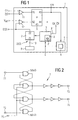
- FIG. 1 shows an embodiment of the integrated according to the invention Circuit arranged on a semiconductor chip 1 is.
- the integrated circuit is in a memory circuit of type DRAM included, for example in a DDR SDRAM.
- the integrated memory has a clock signal CK or a complementary clock signal CK on a external connection is supplied.
- the memory also points a so-called data strobe signal DQS, which via a external connection together with data signals to be output of the memory is transferred externally.
- the data strobe signal DQS acts as a data validity signal or data clock signal of the memory for reading out data of memory.
- the integrated circuit also has a drive circuit 3, which is referred to as a DLL circuit.
- the connection 10 for the signal DQS is connected to an oscillator circuit 9.
- the control circuit 3 has an input 31 for the clock signal CK or CK ,
- the control circuit 3 serves to control a controllable driver circuit 2 which has an input 21 which is connected to a connection 10 for the signal DQS and an output 22 for outputting the signal DQS.
- the control circuit 3 generates a type of internal clock signal from the external clock signal CK or CK with a certain phase shift compared to this.
- the driver circuit 2 is thus driven by the internal clock signal.
- signal transitions of the signal DQS are coordinated with signal transitions of the clock signal CK or CK, or the signal transitions are synchronized with one another. There is a certain phase shift of the signal DQS with respect to the externally supplied clock signal CK or CK adjustable. During a read access, the signal DQS is transmitted from the integrated memory to the outside together with data signals to be output.
- the integrated circuit according to FIG. 1 also has a comparison device 4 which has a first input 41 for the clock signal CK or CK and has a second input 42 which is connected to the output 22 of the driver circuit 2.
- An output 43 of the comparison device 4 is used to output an output signal A.
- the output signal A has a first state "H” when a signal transition of the signal at the input 41 occurs before a signal transition of the signal at the input 42. Accordingly, the output signal A has a second state "L” when the signal transition of the signal at input 41 occurs after the signal transition of the signal at input 42.
- the comparison device 4 has a further output 44, which has a signal which indicates the reverse order of the signal transitions via corresponding states. Resetting the comparison device 4 is possible with a corresponding signal at a connection 45.
- the clock signal CK or CK is connected to the input 41 of the comparison device 4 via a differential amplifier 11.
- the signal DQS is also connected to the input 42 of the comparison device 4 via a differential amplifier 12, to which a reference potential V ref is present.
- the integrated circuit also has a functional unit 5 on that with the output 43 of the comparison device 4 and is connected to the control circuit 3.
- the Functional unit 5 is used to set the control circuit 3 based on the state of the output signal A Comparison device 4.
- the functional unit 5 is a Setting the control circuit 3 by means of a electrical signal possible.
- control circuit 3 In the control circuit 3 is a reference value in one Storage unit 8 stored.
- the control function of the control circuit 3 is based on the stored reference value adjustable.
- the memory unit 8 has programmable Elements F in the form of programmable fuses. If a programming of the memory unit 8 by the Functional unit 5 performed, so are the programmable Fuses F in a suitable manner as electrically programmable Fuses executed.
- the Functional unit 5 a self-test unit 6 for analysis of successive states of the output signal A of the comparison device 4.
- the self-test unit 6 is an independent trimming of the drive circuit 3 possible.
- the comparison result is no longer necessary via an external connection or the setting of the control circuit 3 via external connection.
- the self test unit 6 is suitable, a gradual setting of the control circuit 3 based on an analysis result.
- FIG. 2 shows an embodiment of the comparison device 4 shown.
- This has a flip-flop 7 with a first set input 71 and a second set input 72.
- the Set input 71 is connected to input 41 of the comparison device 4, the set input 72 is connected to the input 42 the comparison device 4 connected.
- the flip-flop 7 has an output 73 which is connected to the output 43 of the comparison device 4 is connected. The further exit 44 the comparison device 4 is with an output 74 Toggle switch 7 connected.
- a toggle reset input 75 7 is with the terminal 45 of the comparison device 4 connected.
- the output signal at output 73 of the flip-flop 7 shows which of the signals at the set inputs 71 or 72 first has a signal transition. Until reset the flip-flop 7 is the respective output signal saved at output 73.
Landscapes
- Engineering & Computer Science (AREA)
- General Engineering & Computer Science (AREA)
- Physics & Mathematics (AREA)
- General Physics & Mathematics (AREA)
- Dram (AREA)
- Tests Of Electronic Circuits (AREA)
- For Increasing The Reliability Of Semiconductor Memories (AREA)
- Logic Circuits (AREA)
Abstract
Description
Die vorliegende Erfindung betrifft eine integrierte Schaltung mit einem Anschluß für ein digitales Signal, mit einer steuerbaren Treiberschaltung, die einen Eingang aufweist, der mit dem Anschluß für das digitale Signal verbunden ist, und einen Ausgang zur Ausgabe des digitalen Signals, und mit einer Ansteuerungsschaltung, die einen Eingang für ein Taktsignal aufweist, zur Ansteuerung der Treiberschaltung in Abhängigkeit des Taktsignals.The present invention relates to an integrated circuit with a connection for a digital signal, with a controllable Driver circuit, which has an input with the connector for the digital signal is connected, and one Output for outputting the digital signal, and with a control circuit, which is an input for a clock signal has to control the driver circuit in dependence of the clock signal.
Im Betrieb von integrierten Schaltungen ist es häufig erforderlich, ein digitales Signal so zu erzeugen oder einzustellen, daß der Zeitpunkt einer Schaltflanke des digitalen Signals an einen Zeitpunkt einer Schaltflanke eines Taktsignals angepaßt ist. Beispielsweise wird das digitale Signal von einer Oszillatorschaltung erzeugt. Die Frequenz des von der Oszillatorschaltung erzeugten Signals ist dabei so einzustellen, daß sie mit der Frequenz des Taktsignals als Bezugsfrequenz übereinstimmt, insbesondere so genau, daß eine vorhandene Phasenverschiebung gleich bleibt.In the operation of integrated circuits, it is often necessary generate or adjust a digital signal so that the timing of a switching edge of the digital signal at a point in time of a switching edge of a clock signal is adjusted. For example, the digital signal from one Oscillator circuit generated. The frequency of that from the oscillator circuit generated signal is to be set so that they are with the frequency of the clock signal as the reference frequency matches, especially so precisely that an existing one Phase shift remains the same.
Eine integrierte Schaltung weist zu diesem Zweck neben einem Anschluß für das digitale Signal beispielsweise eine steuerbare Treiberschaltung auf, die mit dem Anschluß für das digitale Signal verbunden ist, und die zur Ausgabe des digitalen Signals dient. Die Treiberschaltung wird dabei durch eine Ansteuerungsschaltung angesteuert, die einen Eingang für ein Taktsignal aufweist.An integrated circuit has one for this purpose Connection for the digital signal, for example, a controllable Driver circuit on that with the connector for the digital Signal is connected, and which is used to output the digital Signal is used. The driver circuit is activated by a control circuit driven which is an input for a Has clock signal.
Die Ansteuerungsschaltung ist beispielsweise in einem gewissen Bereich anhand eines Referenzwertes einstellbar, um insbesondere Einflüsse von Prozeßschwankungen und Temperaturschwankungen kompensieren zu können. Das bedeutet, im Zuge der Herstellung von derartigen integrierten Schaltungen werden die jeweiligen Referenzwerte jeweils getrennt für jede der integrierten Schaltungen eingestellt und damit angepaßt. Dazu wird der Referenzwert in geeigneter Weise so verändert, daß die unterschiedlichen Einflüsse kompensiert sind. Die Ansteuerungsschaltung wird also ausgehend von dem Referenzwert derart getrimmt, so daß die erforderliche Signalsynchronisation eingestellt ist.The drive circuit is, for example, in a certain Range adjustable based on a reference value, in particular Influences of process fluctuations and temperature fluctuations to be able to compensate. That means on the train the manufacture of such integrated circuits the respective reference values separately for each of the integrated circuits set and thus adjusted. For this purpose, the reference value is changed in a suitable manner, that the different influences are compensated. The control circuit is based on the reference value trimmed so that the required signal synchronization is set.
Zur Einstellung der Ansteuerungsschaltung wird die integrierte Schaltung, die beispielsweise Bestandteil eines integrierten Speichers ist, einem diesbezüglichen Test unterzogen. Dieser Test wird beispielsweise von extern mittels eines dafür vorgesehenen Testsystems durchgeführt. Anhand eines Testergebnisses werden Vorgaben zur Einstellung der Ansteuerungsschaltung definiert. Dazu werden die Schaltflanken des entsprechenden digitalen Signals und des Taktsignals miteinander verglichen und durch Einstellung der Ansteuerungsschaltung zeitlich abgeglichen. Die erreichbare Genauigkeit wird dabei im allgemeinen begrenzt durch Toleranzen des verwendeten Testsystems und der gesamten Testanordnung. Dies kann zur Folge haben, daß eine erforderliche Produktspezifikation der integrierten Schaltung und damit des integrierten Speichers nicht erfüllt ist.To set the control circuit, the integrated Circuit that, for example, part of an integrated Storage is subjected to a test in this regard. This test is carried out, for example, externally using one for this provided test system performed. Based on a test result are specifications for setting the control circuit Are defined. The switching edges of the corresponding digital signal and the clock signal with each other compared and by setting the drive circuit timed. The achievable accuracy will generally limited by tolerances of the used Test system and the entire test arrangement. This can lead to Consequence that a required product specification of the integrated circuit and thus the integrated memory is not fulfilled.
Die Aufgabe der vorliegenden Erfindung ist es, eine integrierte Schaltung der eingangs genannten Art anzugeben, bei der in einem Testbetrieb ein zeitlicher Vergleich von Schaltflanken des Taktsignals und des digitalen Signals am Ausgang der steuerbaren Treiberschaltung mit einer vergleichsweise hohen Genauigkeit durchführbar ist.The object of the present invention is an integrated Specify circuit of the type mentioned at the beginning a time comparison of switching edges in a test operation of the clock signal and the digital signal at the output the controllable driver circuit with a comparatively high accuracy is feasible.
Die Aufgabe wird gelöst durch eine integrierte Schaltung mit einem Anschluß für ein digitales Signal, mit einer steuerbaren Treiberschaltung, die einen Eingang aufweist, der mit dem Anschluß für das digitale Signal verbunden ist, und die einen Ausgang aufweist zur Ausgabe des digitalen Signals, und mit einer Ansteuerungsschaltung, die einen Eingang für ein Taktsignal aufweist, zur Ansteuerung der Treiberschaltung in Abhängigkeit des Taktsignals; bei der die integrierte Schaltung eine Vergleichseinrichtung aufweist, die einen ersten Eingang für das Taktsignal und einen zweiten Eingang aufweist, der mit dem Ausgang der Treiberschaltung verbunden ist, und die einen Ausgang aufweist zur Ausgabe eines Ausgangssignals; bei der das Ausgangssignal der Vergleichseinrichtung ein ersten Zustand aufweist, wenn ein Signalübergang des Signals am ersten Eingang vor einem Signalübergang des Signals am zweiten Eingang erfolgt; und bei der das Ausgangssignal der Vergleichseinrichtung einen zweiten Zustand aufweist, wenn der Signalübergang des Signals am ersten Eingang nach dem Signalübergang des Signals am zweiten Eingang erfolgt.The task is solved by an integrated circuit with a connection for a digital signal, with a controllable Driver circuit which has an input which is connected to the Connection for the digital signal is connected, and the one Output has to output the digital signal, and with a drive circuit that has an input for a clock signal has to control the driver circuit in dependence the clock signal; where the integrated circuit a comparison device having a first input for the clock signal and a second input which is connected to the output of the driver circuit, and the has an output for outputting an output signal; at the output signal of the comparison device is a first Has state when a signal transition of the signal on the first Input before a signal transition of the signal on the second Input occurs; and in which the output signal of the comparison device has a second state when the Signal transition of the signal at the first input after the signal transition of the signal at the second input.
Vorteilhafte Aus- und Weiterbildungen sind Gegenstand abhängiger Ansprüche.Advantageous training and further education are subject dependent Expectations.
Ein zeitlicher Vergleich der Signalübergänge bzw. Schaltflanken des digitalen Signals am Ausgang der Treiberschaltung und des Taktsignals erfolgt durch die Vergleichseinrichtung, die Bestandteil der integrierten Schaltung ist. Das Ausgangssignal der Vergleichseinrichtung zeigt dabei an, welches der Signale an den Eingängen der Vergleichseinrichtung zuerst einen Signalübergang aufweist. Das Ausgangssignal der Vergleichseinrichtung liegt beispielsweise an einem Anschluß für eine externe Analyseeinrichtung an. Dort wird der Zustand eines entnommenen Ausgangssignals der Vergleichseinrichtung analysiert, woraufhin eine Einstellung der Ansteuerungsschaltung anhand des Analyseergebnisses in erforderlicher Weise erfolgen kann.A temporal comparison of the signal transitions or switching edges the digital signal at the output of the driver circuit and of the clock signal is carried out by the comparison device, the Is part of the integrated circuit. The output signal the comparison device shows which of the Signals at the inputs of the comparison device first one Has signal transition. The output signal of the comparison device is, for example, a connection for an external analysis facility. There the state becomes a taken output signal of the comparison device analyzed, whereupon a setting of the drive circuit based on the analysis result in the required manner can be done.
Da bei der Durchführung des zeitlichen Vergleichs des digitalen Signals und des Taktsignals die entsprechenden Signalübergänge nicht durch ein externes Testsystem direkt gemessen und analysiert werden, wird eine höhere Genauigkeit der Messung erreicht. Da die Messung direkt auf dem Chip der integrierten Schaltung erfolgt, ist die Meßgenauigkeit nicht durch die Toleranz eines externen Testsystems und der gesamten Testanordnung begrenzt.Because when performing the time comparison of the digital Signal and the clock signal, the corresponding signal transitions not measured directly by an external test system and being analyzed will be more accurate the measurement reached. Since the measurement is made directly on the chip integrated circuit, the measurement accuracy is not through the tolerance of an external test system and the whole Test setup limited.
Ein entsprechender Zustand des Ausgangssignals der Vergleichseinrichtung ist in vorteilhafter Weise in der Vergleichseinrichtung gespeichert. Dadurch kann das Ausgangssignal der Vergleichseinrichtung während eines längeren Zeitraums beispielsweise durch die externe Analyseeinrichtung entnommen werden. Das Ausgangssignal der Vergleichseinrichtung weist zudem einen statischen Zustand auf, so daß Störeinflüsse bei der Entnahme des Ausgangssignals nicht wesentlich zu einer Verfälschung des Vergleichsergebnisses führen.A corresponding state of the output signal of the comparison device is advantageously in the comparison device saved. This allows the output signal the comparison device for a longer period of time for example by the external analysis device be removed. The output signal of the comparison device also has a static state, so that interference not essential when taking the output signal lead to a falsification of the comparison result.
Die Steuerungsfunktion der Ansteuerungsschaltung ist beispielsweise ausgehend von einem Referenzwert einstellbar. Damit der Referenzwert nur einmal eingestellt werden muß, ist es vorteilhaft, daß der Referenzwert in einer Speichereinheit der Ansteuerungsschaltung gespeichert ist. Die Speichereinheit weist dann beispielsweise programmierbare Elemente in Form von Laser Fuses oder elektrisch programmierbaren Fuses auf. Zur Einstellung des Referenzwertes werden die Laser Fuses von einem sogenannten Lasercutter programmiert.The control function of the control circuit is, for example adjustable based on a reference value. In order to the reference value only needs to be set once it is advantageous that the reference value in a storage unit the control circuit is stored. The storage unit then has, for example, programmable elements in Form of laser fuses or electrically programmable fuses on. The laser fuses are used to set the reference value programmed by a so-called laser cutter.
Die integrierte Schaltung ist zum Beispiel Bestandteil eines integrierten Speichers, beispielsweise eines sogenannten SDRAMs (Synchronous DRAM). Dabei weisen insbesondere sogenannte DDR SDRAM (Double-Data-Rate SDRAMs) vergleichsweise hohe Schalt- und Zugriffsgeschwindigkeiten auf. Derartige integrierte Speicher weisen üblicherweise neben einem Taktsignal, das üblicherweise von extern zugeführt ist, ein Daten-Gültigkeitssignal bzw. Daten-Taktsignal ("Data-Strobe") auf, das an einem externen Anschluß anliegt, beispielsweise zum Auslesen von Daten des integrierten Speichers. Dieses Data-Strobe-Signal wird während eines Lesezugriffs zusammen mit auszugebenden Datensignalen vom integrierten Speicher nach extern übertragen. The integrated circuit is, for example, part of a integrated memory, for example a so-called SDRAMs (Synchronous DRAM). In particular, so-called DDR SDRAM (Double Data Rate SDRAMs) comparatively high switching and access speeds. Such integrated In addition to a clock signal, memories usually have which is usually supplied externally, a data validity signal or data clock signal ("data strobe"), which is connected to an external connection, for example to Reading data from the integrated memory. This data strobe signal is read together with data signals to be output from the integrated memory transmitted externally.
Die Schaltflanken des Data-Strobe-Signals sind mittels einer sogenannten DLL-Schaltung ("Delay-Locked-Loop") mit den Schaltflanken des Taktsignals synchronisiert. Beispielsweise weist das Data-Strobe-Signal gleichzeitig eine Schaltflanke mit dem Taktsignal auf. Die DLL-Schaltung dient als Ansteuerungsschaltung für eine Treiberschaltung, die das Data-Strobe-Signal ausgibt, das beispielsweise durch eine Oszillatorschaltung erzeugt ist und am Eingang der Treiberschaltung anliegt. Über die DLL-Schaltung wird damit eine Art internes Taktsignal aus dem externen Taktsignal erzeugt, das an der Treiberschaltung anliegt. Somit ist eine bestimmte Phasenverschiebung des internen Taktsignals bzw. des Data-Strobe-Signals gegenüber dem extern zugeführten Taktsignal einstellbar.The switching edges of the data strobe signal are by means of a So-called DLL circuit ("Delay-Locked-Loop") with the Switching edges of the clock signal synchronized. For example the data strobe signal has a switching edge at the same time with the clock signal. The DLL circuit serves as a control circuit for a driver circuit that has the data strobe signal outputs that, for example, by an oscillator circuit is generated and at the input of the driver circuit is present. A kind of internal Clock signal generated from the external clock signal that at the Driver circuit is present. So there is a certain phase shift the internal clock signal or the data strobe signal adjustable compared to the externally supplied clock signal.
In einer Ausführungsform der Erfindung ist der erste Eingang der Vergleichseinrichtung mit einem ersten Setz-Eingang einer Kippschaltung und der zweite Eingang der Vergleichseinrichtung mit einem zweiten Setz-Eingang der Kippschaltung verbunden. Der Ausgang der Vergleichseinrichtung ist mit einem Ausgang der Kippschaltung verbunden. Das Ausgangssignal der Kippschaltung zeigt dabei an, welches der Signale an den Setz-Eingängen zuerst einen Signalübergang aufweist.In one embodiment of the invention is the first input the comparison device with a first setting input Toggle switch and the second input of the comparison device connected to a second set input of the multivibrator. The output of the comparison device is with an output the flip-flop connected. The output signal of the Toggle switch shows which of the signals to the Set inputs first have a signal transition.
In einer Weiterbildung der Erfindung weist die integrierte Schaltung eine Funktionseinheit auf, die mit dem Ausgang der Vergleichseinrichtung und mit der Ansteuerungsschaltung verbunden ist. Die Funktionseinheit dient zur Einstellung der Ansteuerungsschaltung anhand des Zustands des Ausgangssignals der Vergleichseinrichtung. Dadurch ist es möglich, die Ansteuerungsschaltung beispielsweise mittels elektrischer Signale einzustellen. Da die Funktionseinheit Teil der integrierten Schaltung ist, müssen keine externen Anschlüsse der integrierten Schaltung vorgesehen werden, um eine elektrische Einstellung der Ansteuerungsschaltung durchzuführen. Außerdem sind geringere Testzeiten zu erreichen, da mehrere Schaltungen parallel getrimmt werden können. Mit der Funktionseinheit können beispielsweise elektrisch programmierbare Fuses, die in der Ansteuerungsschaltung enthalten sind, programmiert werden.In a development of the invention, the integrated Circuit a functional unit on that with the output of the Comparison device and connected to the control circuit is. The functional unit is used to set the Control circuit based on the state of the output signal the comparison device. This enables the control circuit for example by means of electrical signals adjust. Since the functional unit is part of the integrated Circuit, no external connections need to be made integrated circuit can be provided to an electrical Perform setting of the control circuit. Moreover shorter test times can be achieved because there are several circuits can be trimmed in parallel. With the functional unit can, for example, electrically programmable fuses are contained in the control circuit, programmed become.
In einer Weiterbildung der Erfindung weist die Funktionseinheit eine Selbsttesteinheit auf, mit der jeweils aufeinanderfolgende Zustände des Ausgangssignals der Vergleichseinrichtung analysiert werden können. Die Selbsttesteinheit dient außerdem zur schrittweisen Einstellung der Ansteuerungsschaltung anhand eines Analyseergebnisses. Mittels der Selbsttesteinheit ist folglich eine völlig eigenständige Trimmung der Ansteuerungsschaltung möglich. Die Selbsttesteinheit ist dabei nach dem Prinzip des "Built-In-Self-Test" (BIST) realisiert. Die Testzeit von mehreren zu testenden integrierten Schaltungen kann dadurch wesentlich verkürzt werden. Es können Ansteuerungsschaltungen von mehreren integrierten Schaltungen parallel getrimmt werden.In a development of the invention, the functional unit a self-test unit, with the successive one States of the output signal of the comparison device can be analyzed. The self-test unit serves also for the gradual setting of the control circuit based on an analysis result. By means of the self-test unit is therefore a completely independent trim Control circuit possible. The self-test unit is included realized according to the principle of the "Built-In-Self-Test" (BIST). The test time of several integrated to be tested Circuits can be shortened considerably. It can Control circuits of several integrated circuits be trimmed in parallel.
Die Erfindung wird im folgenden anhand der in der Zeichnung dargestellten Figuren näher erläutert. Es zeigen:
- Figur 1
- eine Ausführungsform der Erfindung,
- Figur 2
- eine Ausführungsform der Vergleichseinrichtung.
- Figure 1
- one embodiment of the invention,
- Figure 2
- an embodiment of the comparison device.
Figur 1 zeigt eine Ausführungsform der erfindungsgemäßen integrierten Schaltung, die auf einem Halbleiterchip 1 angeordnet ist. Die integrierte Schaltung ist in einer Speicherschaltung von Typ DRAM enthalten, beispielsweise in einem DDR SDRAM. Der integrierte Speicher weist ein Taktsignal CK bzw. ein dazu komplementäres Taktsignal CK auf, das über einen externen Anschluß zugeführt ist. Der Speicher weist außerdem ein sogenanntes Data-Strobe-Signal DQS auf, das über einen externen Anschluß zusammen mit auszugebenden Datensignalen des Speichers nach extern übertragen wird. Das Data-Strobe-Signal DQS fungiert dabei als ein Daten-Gültigkeitssignal bzw. Daten-Taktsignal des Speichers zum Auslesen von Daten des Speichers.Figure 1 shows an embodiment of the integrated according to the invention Circuit arranged on a semiconductor chip 1 is. The integrated circuit is in a memory circuit of type DRAM included, for example in a DDR SDRAM. The integrated memory has a clock signal CK or a complementary clock signal CK on a external connection is supplied. The memory also points a so-called data strobe signal DQS, which via a external connection together with data signals to be output of the memory is transferred externally. The data strobe signal DQS acts as a data validity signal or data clock signal of the memory for reading out data of memory.
Die integrierte Schaltung weist weiterhin eine Ansteuerungsschaltung
3 auf, die als DLL-Schaltung bezeichnet wird. Der
Anschluß 10 für das Signal DQS ist an eine Oszillatorschaltung
9 angeschlossen. Die Ansteuerungsschaltung 3 weist einen
Eingang 31 auf für das Taktsignal CK bzw.
Die integrierte Schaltung nach Figur 1 weist weiterhin eine
Vergleichseinrichtung 4 auf, die einen ersten Eingang 41 für
das Taktsignal CK bzw.
Das Taktsignal CK bzw.
Die integrierte Schaltung weist weiterhin eine Funktionseinheit
5 auf, die mit dem Ausgang 43 der Vergleichseinrichtung
4 und mit der Ansteuerungsschaltung 3 verbunden ist. Die
Funktionseinheit 5 dient zur Einstellung der Ansteuerungsschaltung
3 anhand des Zustands des Ausgangssignals A der
Vergleichseinrichtung 4. Durch die Funktionseinheit 5 ist eine
Einstellung der Ansteuerungsschaltung 3 mittels eines
elektrischen Signals möglich.The integrated circuit also has a
In der Ansteuerungsschaltung 3 ist ein Referenzwert in einer
Speichereinheit 8 gespeichert. Die Steuerungsfunktion der Ansteuerungsschaltung
3 ist ausgehend von dem gespeicherten Referenzwert
einstellbar. Die Speichereinheit 8 weist programmierbare
Elemente F in Form von programmierbaren Fuses auf.
Wird eine Programmierung der Speichereinheit 8 durch die
Funktionseinheit 5 durchgeführt, so sind die programmierbaren
Fuses F in geeigneter Weise als elektrisch programmierbare
Fuses ausgeführt.In the
In einer Weiterbildung der integrierten Schaltung weist die
Funktionseinheit 5 eine Selbsttesteinheit 6 auf zur Analyse
von jeweils aufeinanderfolgenden Zuständen des Ausgangssignals
A der Vergleichseinrichtung 4. Mittels der Selbsttesteinheit
6 ist ein eigenständiges Trimmen der Ansteuerungsschaltung
3 möglich. Es ist nicht mehr erforderlich, das Vergleichsergebnis
über einen externen Anschluß zu entnehmen
bzw. die Einstellung der Ansteuerungsschaltung 3 über einen
externen Anschluß durchzuführen. Die Selbsttesteinheit 6 ist
geeignet, eine schrittweise Einstellung der Ansteuerungsschaltung
3 anhand eines Analyseergebnisses vorzunehmen.In a further development of the integrated circuit, the
Functional unit 5 a self-
In Figur 2 ist eine Ausführungsform der Vergleichseinrichtung
4 dargestellt. Diese weist eine Kippschaltung 7 auf mit einem
ersten Setz-Eingang 71 und einem zweiten Setz-Eingang 72. Der
Setz-Eingang 71 ist mit dem Eingang 41 der Vergleichseinrichtung
4 verbunden, der Setz-Eingang 72 ist mit dem Eingang 42
der Vergleichseinrichtung 4 verbunden. Die Kippschaltung 7
weist einen Ausgang 73 auf, der mit dem Ausgang 43 der Vergleichseinrichtung
4 verbunden ist. Der weitere Ausgang 44
der Vergleichseinrichtung 4 ist mit einem Ausgang 74 der
Kippschaltung 7 verbunden. Ein Rücksetz-Eingang 75 der Kippschaltung
7 ist mit dem Anschluß 45 der Vergleichseinrichtung
4 verbunden. Das Ausgangssignal am Ausgang 73 der Kippschaltung
7 zeigt an, welches der Signale an den Setz-Eingängen 71
bzw. 72 zuerst einen Signalübergang aufweist. Bis zum Rücksetzen
der Kippschaltung 7 ist das jeweilige Ausgangssignal
am Ausgang 73 gespeichert.FIG. 2 shows an embodiment of the
Claims (10)
dadurch gekennzeichnet, daß
die Zustände des Ausgangssignals (A) der Vergleichseinrichtung (4) in der Vergleichseinrichtung (4) gespeichert sind.Integrated circuit according to Claim 1,
characterized in that
the states of the output signal (A) of the comparison device (4) are stored in the comparison device (4).
dadurch gekennzeichnet, daß
characterized in that
dadurch gekennzeichnet, daß
die integrierte Schaltung eine Funktionseinheit (5) aufweist, die mit dem Ausgang (43) der Vergleichseinrichtung (4) und mit der Ansteuerungsschaltung (3) verbunden ist, zur Einstellung einer Steuerungsfunktion der Ansteuerungsschaltung (3) anhand des Zustands des Ausgangssignals (A) der Vergleichseinrichtung (4).Integrated circuit according to one of the preceding claims,
characterized in that
the integrated circuit has a functional unit (5) which is connected to the output (43) of the comparison device (4) and to the control circuit (3) for setting a control function of the control circuit (3) on the basis of the state of the output signal (A) Comparison device (4).
dadurch gekennzeichnet, daß
die Funktionseinheit (5) eine Selbsttesteinheit (6) aufweist zur Analyse von jeweils aufeinanderfolgenden Zuständen des Ausgangssignals (A) der Vergleichseinrichtung (4) und zur schrittweisen Einstellung der Ansteuerungsschaltung (3) anhand eines Analyseergebnisses.Integrated circuit according to Claim 4,
characterized in that
the functional unit (5) has a self-test unit (6) for analyzing successive states of the output signal (A) of the comparison device (4) and for step-by-step adjustment of the control circuit (3) based on an analysis result.
dadurch gekennzeichnet, daß
characterized in that
dadurch gekennzeichnet, daß
die Speichereinheit (8) programmierbare Elemente (F) in Form von programmierbaren Fuses aufweist.Integrated circuit according to Claim 6,
characterized in that
the memory unit (8) has programmable elements (F) in the form of programmable fuses.
dadurch gekennzeichnet, daß
am Anschluß (10) für das digitale Signal (DQS) eine Oszillatorschaltung (9) angeschlossen ist.Integrated circuit according to one of the preceding claims,
characterized in that
an oscillator circuit (9) is connected to the connection (10) for the digital signal (DQS).
dadurch gekennzeichnet, daß
die integrierte Schaltung in einer Speicherschaltung vom Typ DRAM enthalten ist.Integrated circuit according to one of the preceding claims,
characterized in that
the integrated circuit is contained in a memory circuit of the DRAM type.
dadurch gekennzeichnet, daß
das digitale Signal (DQS) ein Daten-Gültigkeitssignal und ein Daten-Taktsignal ist zum Auslesen von Daten der Speicherschaltung.Integrated circuit according to Claim 9,
characterized in that
the digital signal (DQS) is a data validity signal and a data clock signal is for reading out data from the memory circuit.
Applications Claiming Priority (2)
| Application Number | Priority Date | Filing Date | Title |
|---|---|---|---|
| DE10014386 | 2000-03-23 | ||
| DE10014386A DE10014386A1 (en) | 2000-03-23 | 2000-03-23 | Integrated circuit with control circuit for controlling a driver circuit |
Publications (2)
| Publication Number | Publication Date |
|---|---|
| EP1136834A2 true EP1136834A2 (en) | 2001-09-26 |
| EP1136834A3 EP1136834A3 (en) | 2005-01-19 |
Family
ID=7636018
Family Applications (1)
| Application Number | Title | Priority Date | Filing Date |
|---|---|---|---|
| EP01104729A Withdrawn EP1136834A3 (en) | 2000-03-23 | 2001-02-26 | Integrated circuit with a control circuit for controlling a driver circuit |
Country Status (4)
| Country | Link |
|---|---|
| US (1) | US6351161B2 (en) |
| EP (1) | EP1136834A3 (en) |
| DE (1) | DE10014386A1 (en) |
| TW (1) | TW525343B (en) |
Families Citing this family (4)
| Publication number | Priority date | Publication date | Assignee | Title |
|---|---|---|---|---|
| US7015300B2 (en) | 1995-06-07 | 2006-03-21 | Acushnet Company | Multilayered golf ball and composition |
| DE602006010915D1 (en) * | 2006-07-17 | 2010-01-14 | Infineon Technologies Ag | ONCHIP CHECK FOR AN EMBEDDED COMPARATOR |
| US20080080266A1 (en) * | 2006-09-27 | 2008-04-03 | Khellah Muhammad M | Memory driver circuits with embedded level shifters |
| US8624653B2 (en) | 2011-06-15 | 2014-01-07 | Freescale Semiconductor, Inc. | Circuit and method for determining comparator offsets of electronic devices |
Family Cites Families (13)
| Publication number | Priority date | Publication date | Assignee | Title |
|---|---|---|---|---|
| DE102027C (en) | ||||
| DD102027A1 (en) * | 1972-12-18 | 1973-11-20 | ||
| US4799023A (en) * | 1981-11-05 | 1989-01-17 | Hewlett-Packard Company | Circuits and apparatus which enable elimination of setup time and hold time testing errors |
| US5471159A (en) * | 1992-09-18 | 1995-11-28 | Tektronix, Inc. | Setup or hold violation triggering |
| US5696951A (en) * | 1996-01-03 | 1997-12-09 | Credence Systems Corporation | Signal deskewing system for synchronous logic circuit |
| US5771264A (en) * | 1996-08-29 | 1998-06-23 | Altera Corporation | Digital delay lock loop for clock signal frequency multiplication |
| US5959481A (en) * | 1997-02-18 | 1999-09-28 | Rambus Inc. | Bus driver circuit including a slew rate indicator circuit having a one shot circuit |
| JPH11265573A (en) * | 1998-01-13 | 1999-09-28 | Mitsubishi Electric Corp | Semiconductor storage device |
| GB9800925D0 (en) * | 1998-01-17 | 1998-03-11 | Lucas Ind Plc | Power switching circuit for use in a power distribution system |
| JPH11306757A (en) * | 1998-04-27 | 1999-11-05 | Mitsubishi Electric Corp | Synchronous semiconductor memory device |
| US6100733A (en) * | 1998-06-09 | 2000-08-08 | Siemens Aktiengesellschaft | Clock latency compensation circuit for DDR timing |
| JP2000076853A (en) * | 1998-06-17 | 2000-03-14 | Mitsubishi Electric Corp | Synchronous semiconductor memory device |
| US6232801B1 (en) * | 1999-08-04 | 2001-05-15 | Vlsi Technology, Inc. | Comparators and comparison methods |
-
2000
- 2000-03-23 DE DE10014386A patent/DE10014386A1/en not_active Ceased
-
2001
- 2001-02-26 EP EP01104729A patent/EP1136834A3/en not_active Withdrawn
- 2001-03-22 TW TW090106784A patent/TW525343B/en not_active IP Right Cessation
- 2001-03-23 US US09/816,935 patent/US6351161B2/en not_active Expired - Lifetime
Also Published As
| Publication number | Publication date |
|---|---|
| DE10014386A1 (en) | 2001-09-27 |
| US20010026173A1 (en) | 2001-10-04 |
| TW525343B (en) | 2003-03-21 |
| EP1136834A3 (en) | 2005-01-19 |
| US6351161B2 (en) | 2002-02-26 |
Similar Documents
| Publication | Publication Date | Title |
|---|---|---|
| DE3587223T2 (en) | Independent matrix timing. | |
| DE69805023T2 (en) | Delay circuit with calibration | |
| DE69904320T2 (en) | ON-CHIP CIRCUIT AND METHOD FOR CHECKING THE MEMORY CIRCUIT | |
| DE10023248B4 (en) | Circuit and method for clock signal synchronization | |
| DE3750597T2 (en) | Calibrated automatic test system. | |
| DE19960244C1 (en) | Arrangement for trimming reference voltages in semiconducting chips enables rapid and cost-effective reference voltage trimming | |
| DE69322751T2 (en) | Fusible link programmable buck converter | |
| DE3788586T2 (en) | Circuit for testing the input voltage signal for a semiconductor integrated circuit. | |
| DE10149104B4 (en) | Semiconductor device for processing data and method for detecting an operating state | |
| EP1136834A2 (en) | Integrated circuit with a control circuit for controlling a driver circuit | |
| DE10318603A1 (en) | Input reception circuit for weak high speed signal for generating several output signals, which can be processed at lower detecting speed | |
| DE10063102A1 (en) | Configuration for measurement of internal voltages in an integrated semiconductor apparatus, using comparator connected to reference voltage | |
| DE10231419B4 (en) | Device and method for calibrating signals | |
| DE19830571A1 (en) | Integrated circuit | |
| DE19839105B4 (en) | Integrated semiconductor memory with control device for isochronous writing and reading | |
| EP1390951B1 (en) | Dynamic memory and method for testing a dynamic memory | |
| DE10032257A1 (en) | Method and device for offset voltage-free voltage measurement of a reference voltage source of an integrated semiconductor circuit | |
| DE10112311A1 (en) | Calibration method and device for correcting pulse width time errors when testing integrated circuits | |
| DE10145745B4 (en) | Integrated circuit and method for its operation | |
| DE10133689C2 (en) | Test method and test device for electronic memories | |
| DE10031946C2 (en) | Integrated circuit with a timer circuit and method for setting an output signal of the timer circuit | |
| DE102005007084B4 (en) | Integrated semiconductor memory with adjustable internal voltage | |
| DE10154812B4 (en) | Circuit for adjusting a signal propagation time of a signal on a signal line | |
| DE10222892B4 (en) | Integrated memory | |
| DE10102349C1 (en) | Method and circuit arrangement for identifying an operating characteristic of an integrated circuit |
Legal Events
| Date | Code | Title | Description |
|---|---|---|---|
| PUAI | Public reference made under article 153(3) epc to a published international application that has entered the european phase |
Free format text: ORIGINAL CODE: 0009012 |
|
| AK | Designated contracting states |
Kind code of ref document: A2 Designated state(s): AT BE CH CY DE DK ES FI FR GB GR IE IT LI LU MC NL PT SE TR |
|
| AX | Request for extension of the european patent |
Free format text: AL;LT;LV;MK;RO;SI |
|
| RIC1 | Information provided on ipc code assigned before grant |
Ipc: 7G 11C 7/22 B Ipc: 7G 11C 7/10 B Ipc: 7G 11C 29/00 B Ipc: 7G 01R 31/3185 A |
|
| PUAL | Search report despatched |
Free format text: ORIGINAL CODE: 0009013 |
|
| AK | Designated contracting states |
Kind code of ref document: A3 Designated state(s): AT BE CH CY DE DK ES FI FR GB GR IE IT LI LU MC NL PT SE TR |
|
| AX | Request for extension of the european patent |
Extension state: AL LT LV MK RO SI |
|
| 17P | Request for examination filed |
Effective date: 20050617 |
|
| AKX | Designation fees paid |
Designated state(s): DE GB IE |
|
| 17Q | First examination report despatched |
Effective date: 20070504 |
|
| STAA | Information on the status of an ep patent application or granted ep patent |
Free format text: STATUS: THE APPLICATION IS DEEMED TO BE WITHDRAWN |
|
| 18D | Application deemed to be withdrawn |
Effective date: 20090901 |