EP1132979A2 - Herstellungsverfahren für piezoelektrische Wandler - Google Patents
Herstellungsverfahren für piezoelektrische Wandler Download PDFInfo
- Publication number
- EP1132979A2 EP1132979A2 EP01302167A EP01302167A EP1132979A2 EP 1132979 A2 EP1132979 A2 EP 1132979A2 EP 01302167 A EP01302167 A EP 01302167A EP 01302167 A EP01302167 A EP 01302167A EP 1132979 A2 EP1132979 A2 EP 1132979A2
- Authority
- EP
- European Patent Office
- Prior art keywords
- piezoelectric
- piezoelectric material
- manufacturing
- actuators
- bodies
- Prior art date
- Legal status (The legal status is an assumption and is not a legal conclusion. Google has not performed a legal analysis and makes no representation as to the accuracy of the status listed.)
- Withdrawn
Links
- 238000004519 manufacturing process Methods 0.000 title claims abstract description 49
- 238000005304 joining Methods 0.000 claims description 13
- 238000004806 packaging method and process Methods 0.000 claims 1
- 230000007246 mechanism Effects 0.000 description 16
- 230000003247 decreasing effect Effects 0.000 description 11
- 238000012545 processing Methods 0.000 description 9
- 230000004048 modification Effects 0.000 description 5
- 238000012986 modification Methods 0.000 description 5
- 238000007796 conventional method Methods 0.000 description 4
- 238000005520 cutting process Methods 0.000 description 3
- 238000000034 method Methods 0.000 description 3
- 238000012856 packing Methods 0.000 description 3
- 230000035515 penetration Effects 0.000 description 2
- 230000008569 process Effects 0.000 description 2
- 230000000881 depressing effect Effects 0.000 description 1
- 230000000994 depressogenic effect Effects 0.000 description 1
- 238000010586 diagram Methods 0.000 description 1
- 238000005530 etching Methods 0.000 description 1
- 238000003980 solgel method Methods 0.000 description 1
- 238000004544 sputter deposition Methods 0.000 description 1
Images






Classifications
-
- H—ELECTRICITY
- H02—GENERATION; CONVERSION OR DISTRIBUTION OF ELECTRIC POWER
- H02N—ELECTRIC MACHINES NOT OTHERWISE PROVIDED FOR
- H02N2/00—Electric machines in general using piezoelectric effect, electrostriction or magnetostriction
- H02N2/10—Electric machines in general using piezoelectric effect, electrostriction or magnetostriction producing rotary motion, e.g. rotary motors
- H02N2/16—Electric machines in general using piezoelectric effect, electrostriction or magnetostriction producing rotary motion, e.g. rotary motors using travelling waves, i.e. Rayleigh surface waves
-
- H—ELECTRICITY
- H10—SEMICONDUCTOR DEVICES; ELECTRIC SOLID-STATE DEVICES NOT OTHERWISE PROVIDED FOR
- H10N—ELECTRIC SOLID-STATE DEVICES NOT OTHERWISE PROVIDED FOR
- H10N30/00—Piezoelectric or electrostrictive devices
- H10N30/01—Manufacture or treatment
- H10N30/03—Assembling devices that include piezoelectric or electrostrictive parts
-
- Y—GENERAL TAGGING OF NEW TECHNOLOGICAL DEVELOPMENTS; GENERAL TAGGING OF CROSS-SECTIONAL TECHNOLOGIES SPANNING OVER SEVERAL SECTIONS OF THE IPC; TECHNICAL SUBJECTS COVERED BY FORMER USPC CROSS-REFERENCE ART COLLECTIONS [XRACs] AND DIGESTS
- Y10—TECHNICAL SUBJECTS COVERED BY FORMER USPC
- Y10T—TECHNICAL SUBJECTS COVERED BY FORMER US CLASSIFICATION
- Y10T29/00—Metal working
- Y10T29/42—Piezoelectric device making
-
- Y—GENERAL TAGGING OF NEW TECHNOLOGICAL DEVELOPMENTS; GENERAL TAGGING OF CROSS-SECTIONAL TECHNOLOGIES SPANNING OVER SEVERAL SECTIONS OF THE IPC; TECHNICAL SUBJECTS COVERED BY FORMER USPC CROSS-REFERENCE ART COLLECTIONS [XRACs] AND DIGESTS
- Y10—TECHNICAL SUBJECTS COVERED BY FORMER USPC
- Y10T—TECHNICAL SUBJECTS COVERED BY FORMER US CLASSIFICATION
- Y10T29/00—Metal working
- Y10T29/49—Method of mechanical manufacture
- Y10T29/49002—Electrical device making
- Y10T29/49004—Electrical device making including measuring or testing of device or component part
-
- Y—GENERAL TAGGING OF NEW TECHNOLOGICAL DEVELOPMENTS; GENERAL TAGGING OF CROSS-SECTIONAL TECHNOLOGIES SPANNING OVER SEVERAL SECTIONS OF THE IPC; TECHNICAL SUBJECTS COVERED BY FORMER USPC CROSS-REFERENCE ART COLLECTIONS [XRACs] AND DIGESTS
- Y10—TECHNICAL SUBJECTS COVERED BY FORMER USPC
- Y10T—TECHNICAL SUBJECTS COVERED BY FORMER US CLASSIFICATION
- Y10T29/00—Metal working
- Y10T29/49—Method of mechanical manufacture
- Y10T29/49002—Electrical device making
- Y10T29/49117—Conductor or circuit manufacturing
- Y10T29/49124—On flat or curved insulated base, e.g., printed circuit, etc.
- Y10T29/49126—Assembling bases
-
- Y—GENERAL TAGGING OF NEW TECHNOLOGICAL DEVELOPMENTS; GENERAL TAGGING OF CROSS-SECTIONAL TECHNOLOGIES SPANNING OVER SEVERAL SECTIONS OF THE IPC; TECHNICAL SUBJECTS COVERED BY FORMER USPC CROSS-REFERENCE ART COLLECTIONS [XRACs] AND DIGESTS
- Y10—TECHNICAL SUBJECTS COVERED BY FORMER USPC
- Y10T—TECHNICAL SUBJECTS COVERED BY FORMER US CLASSIFICATION
- Y10T29/00—Metal working
- Y10T29/49—Method of mechanical manufacture
- Y10T29/49002—Electrical device making
- Y10T29/49117—Conductor or circuit manufacturing
- Y10T29/49124—On flat or curved insulated base, e.g., printed circuit, etc.
- Y10T29/49128—Assembling formed circuit to base
-
- Y—GENERAL TAGGING OF NEW TECHNOLOGICAL DEVELOPMENTS; GENERAL TAGGING OF CROSS-SECTIONAL TECHNOLOGIES SPANNING OVER SEVERAL SECTIONS OF THE IPC; TECHNICAL SUBJECTS COVERED BY FORMER USPC CROSS-REFERENCE ART COLLECTIONS [XRACs] AND DIGESTS
- Y10—TECHNICAL SUBJECTS COVERED BY FORMER USPC
- Y10T—TECHNICAL SUBJECTS COVERED BY FORMER US CLASSIFICATION
- Y10T29/00—Metal working
- Y10T29/49—Method of mechanical manufacture
- Y10T29/49002—Electrical device making
- Y10T29/49117—Conductor or circuit manufacturing
- Y10T29/49124—On flat or curved insulated base, e.g., printed circuit, etc.
- Y10T29/49147—Assembling terminal to base
-
- Y—GENERAL TAGGING OF NEW TECHNOLOGICAL DEVELOPMENTS; GENERAL TAGGING OF CROSS-SECTIONAL TECHNOLOGIES SPANNING OVER SEVERAL SECTIONS OF THE IPC; TECHNICAL SUBJECTS COVERED BY FORMER USPC CROSS-REFERENCE ART COLLECTIONS [XRACs] AND DIGESTS
- Y10—TECHNICAL SUBJECTS COVERED BY FORMER USPC
- Y10T—TECHNICAL SUBJECTS COVERED BY FORMER US CLASSIFICATION
- Y10T29/00—Metal working
- Y10T29/49—Method of mechanical manufacture
- Y10T29/49002—Electrical device making
- Y10T29/49117—Conductor or circuit manufacturing
- Y10T29/49124—On flat or curved insulated base, e.g., printed circuit, etc.
- Y10T29/49155—Manufacturing circuit on or in base
-
- Y—GENERAL TAGGING OF NEW TECHNOLOGICAL DEVELOPMENTS; GENERAL TAGGING OF CROSS-SECTIONAL TECHNOLOGIES SPANNING OVER SEVERAL SECTIONS OF THE IPC; TECHNICAL SUBJECTS COVERED BY FORMER USPC CROSS-REFERENCE ART COLLECTIONS [XRACs] AND DIGESTS
- Y10—TECHNICAL SUBJECTS COVERED BY FORMER USPC
- Y10T—TECHNICAL SUBJECTS COVERED BY FORMER US CLASSIFICATION
- Y10T29/00—Metal working
- Y10T29/49—Method of mechanical manufacture
- Y10T29/49789—Obtaining plural product pieces from unitary workpiece
-
- Y—GENERAL TAGGING OF NEW TECHNOLOGICAL DEVELOPMENTS; GENERAL TAGGING OF CROSS-SECTIONAL TECHNOLOGIES SPANNING OVER SEVERAL SECTIONS OF THE IPC; TECHNICAL SUBJECTS COVERED BY FORMER USPC CROSS-REFERENCE ART COLLECTIONS [XRACs] AND DIGESTS
- Y10—TECHNICAL SUBJECTS COVERED BY FORMER USPC
- Y10T—TECHNICAL SUBJECTS COVERED BY FORMER US CLASSIFICATION
- Y10T29/00—Metal working
- Y10T29/49—Method of mechanical manufacture
- Y10T29/49789—Obtaining plural product pieces from unitary workpiece
- Y10T29/49798—Dividing sequentially from leading end, e.g., by cutting or breaking
Definitions
- the present invention relates to piezoelectric actuators and, in particular, to a method of manufacturing a piezoelectric actuator.
- a piezoelectric material is divided by a predetermined size, and then various processings such as poling processing and joining of various parts are performed for each divided piezoelectric material.
- each of structure parts of the piezoelectric actuator is also miniaturized.
- assembly of the piezoelectric actuator takes a long time, production efficiency becomes low and a manufacturing cost becomes high.
- An object of the present invention is to provide a method of manufacturing a piezoelectric actuator, which has high production efficiency and is available to miniaturize the piezoelectric actuator. Also, an object of the present invention is to simply pack the piezoelectric actuator and to easily perform a quality examination before shipment.
- a method of manufacturing a piezoelectric actuator characterized by including the steps of joining parts except for piezoelectric bodies to a piezoelectric material having a size such that a plurality of piezoelectric actuators can be formed thereon, so as form the plurality of piezoelectric actuators, providing the piezoelectric material with a predetermined poling structure, and then dividing the piezoelectric material to form the plurality of piezoelectric actuators.
- joinings of the parts except for the piezoelectric bodies are performed by, for example, a step of forming electrodes having predetermined shapes on both surfaces of a piezoelectric material having a size that a plurality of piezoelectric actuators can be formed, a step of joining vibrating bodies to the piezoelectric material, a step of setting moving bodies so as to be actuated by vibration transmitted from the vibrating bodies, and a step of setting pressuring means for pressuring the moving bodies toward the vibrating bodies.
- the piezoelectric material is divided to manufacture the plurality of piezoelectric actuators.
- a part sheet including a plurality of identical parts in predetermined positions is layered on the piezoelectric material to join at least one kind of the parts.
- the number of steps can be further decreased and miniaturization of each of the piezoelectric actuators can be sufficiently applied.
- the piezoelectric material may be transported to a place where the piezoelectric actuator is to be used, and divided into the plurality of piezoelectric actuators to use them in the place.
- FIG. 1 is a cross sectional view of the piezoelectric actuator 1 manufactured by the manufacturing method of the present invention.
- the piezoelectric actuator 1 is constructed of a piezoelectric body 11, a vibrating body 14 which is joined on an upper surface of the piezoelectric body 11, a plurality of protrusions 14a which are integrally provided on an upper surface of the vibrating body 14, a supporting part 15 which is passed through the centers of the piezoelectric body 11 and the vibrating body 14, a moving body 16 which is disposed to contact against the protrusions 14a, a pressuring mechanism 17 whose tip narrow portion (mentioned below)is fitted to a groove portion 16a of the moving body 16, which has functions for positioning the moving body 16 and supporting the supporting part 15 with rotation, and which presses the moving body 16 to the protrusions 14a, and a holding part 18 for adjusting a pressure applied to the pressuring mechanism 17 and capping a tip of the supporting part 15.
- a plurality of identical parts constituting the piezoelectric actuator 1 are formed as part sheets disposed on one surface. Also, a piezoelectric material sheet formed with a predetermined shape is performed with various processings such as poling processing, and each of the part sheets is joined onto the piezoelectric material sheet. Thus, the resultant piezoelectric material sheet with a plurality of piezoelectric actuators is manufactured, and then divided into each piezoelectric actuator 1.
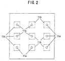
- a piezoelectric material sheet 111 shown in FIG. 2 is formed with a size and a form such that nine piezoelectric actuators 1 can be formed. That is, the piezoelectric material sheet 111 has a size such that nine piezoelectric bodies 11 can be taken. Each of holes 11a into which the supporting part 15 mentioned below is inserted is formed with penetration in the center of each of regions 11b as the piezoelectric bodies 11.
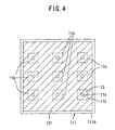
- a dividing electrode pattern 121 is formed on one surface 111a of the piezoelectric material sheet 111.
- Each of dividing electrode patterns 12 including electrode patterns 12a to 12d is formed on one surface of each of the piezoelectric bodies 11.
- an entire surface electrode pattern 131 is formed on the other surface 111b of the piezoelectric material sheet 111.
- each of entire surface electrode patterns 13 is formed on the other surface of each of the piezoelectric bodies 11.
- a process such as sputtering or a sol-gel method is used to form the dividing electrode pattern 121 and the entire surface electrode pattern 131.
- the electrode patterns 121 and 131 can be also formed simultaneously.
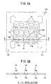
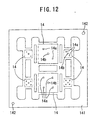
- a vibrating body sheet 141 shown in FIGS. 5A and 5B has nine vibrating bodies 14.
- a position of each of the vibrating bodies 14 corresponds to a position of each of the piezoelectric bodies 11 of the piezoelectric material sheet 111.
- Each of holes 14b into which the supporting part 15 mentioned below is inserted is formed with penetration in the center of each of the vibrating bodies 14.
- two protrusions 14a are formed in symmetric positions sandwiching the hole 14b.
- the protrusions 14a are formed by depressing a portion around the protrusions 14a with cutting (see FIG. 5B), further in order to decrease a load applied in dividing mentioned below, a region around the portion is depressed with cutting.
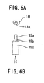
- the supporting part 15 shown in FIG. 6B is constructed of three cylindrical portions 15a, 15b and 15c with different cross section areas.
- the outside diameter of the cylindrical portion 15a is set to approximately equal to the diameter of a hole 17b of the pressuring mechanism 17 mentioned below.
- the outside diameter of the cylindrical portion 15b is set to approximately equal to the diameter of the hole 14a of the vibrating body 14.
- the outside diameter of the cylindrical portion 15c is set to approximately equal to the diameter of the hole 11a of the piezoelectric body 11.
- the holding part 18 shown in FIG. 6A is joined by fitting a concave portion 18a into a tip of the cylindrical portion 15a of the supporting part 15 in step S9 mentioned below (see FIG. 10).
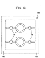
- a moving body sheet 161 shown in FIGS. 7A and 7B has nine moving bodies 16.
- a position of each of the moving bodies 16 corresponds to a position of each of the piezoelectric bodies 11 of the piezoelectric material sheet 111.
- the three groove portions 16a are formed in each of the moving bodies 16 at regular intervals by a method such as etching or cutting.
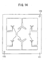
- a pressuring mechanism sheet 171 shown in FIG. 8 has nine pressuring mechanisms 17.
- a position of each of the pressuring mechanisms 17 corresponds to a position of each of the piezoelectric bodies 11 of the piezoelectric material sheet 111.
- Three tip narrow portions 17a which are fitted into the groove portions 16a of each of the moving bodies 16 are formed in each of the pressuring mechanisms 17.
- Each of the holes 17b into which the supporting part 15 is inserted is formed in the center of each of the pressuring mechanisms 17.
- shafts provided in a jig (not shown) for assembly are inserted into holes 142, 162 and 172 which are formed in the vibrating body sheet 141, the moving body sheet 161 and the pressuring mechanism sheet 171, respectively. Each part sheet is assembled on the jig.
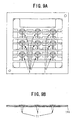
- the above part sheets are joined onto the piezoelectric material sheet 111 in accordance with a flowchart of FIG. 10 mentioned below to simultaneously manufacture nine piezoelectric actuators 1 as shown in FIGS. 9A and 9B.
- a piezoelectric material is processed to obtain the piezoelectric material sheet 111 with a predetermined shape (step S1).
- the dividing electrode pattern 121 is formed on the surface 111a of the piezoelectric material sheet 111 (step S2), and the entire surface electrode pattern 131 is formed on the other surface 111b of the piezoelectric material sheet 111 (step S3).
- steps S2 and 53 may be performed simultaneously, or the electrode patterns 121 and 131 may be formed in the reverse order to the above.
- a predetermined voltage is applied to the electrode patterns 121 and 131 formed on both surfaces of the piezoelectric material sheet 111 to form the piezoelectric material sheet 111 (piezoelectric bodies 11) with a predetermined poling structure (step S4).
- step S5 the piezoelectric material sheet 111 is joined to the vibrating body sheet 141 such that the holes 11a and 14b formed in each part sheet overlap each other.
- step S6 the supporting parts 15 are joined to the piezoelectric material sheet 111 and the vibrating body sheet 141, which are joined to each other.
- the supporting parts 15 are inserted into the holes 11a of the piezoelectric material sheet 111 and the holes 14b of the moving body sheet 141 from the side of the other surface 111b of the piezoelectric material sheet 111. Note that, since the inside diameter of each of the holes 14b is smaller than the outside diameter of the cylindrical portion 15c of each of the supporting parts 15, the supporting parts 15 do not penetrate the vibrating body sheet 141.
- the moving body sheet 161 is set on the vibrating body sheet 141 such that the moving bodies 16 contact the protrusions 14a of the vibrating bodies 14 (step S7).
- the tip narrow portions 17a of the pressuring mechanisms 17 are fitted to the groove portions 16a of the moving bodies 16 to set the pressuring mechanism sheet 171 onto the moving body sheet 161 (step S8).
- fitting of the tip narrow portions 17a to the groove portions 16a combines with inter-alignment.
- step S9 With a state that the pressuring mechanisms 17 are warped and pressured such that the moving bodies 16 are pushed to the protrusions 14a with a predetermined pressure, the holding parts 18 are joined onto the supporting parts 15 (step S9).
- the piezoelectric material sheet 111 is divided by dicing, blanking or the like, or by processing with an excimer laser (step S10), so that nine piezoelectric actuators 1 shown in FIG. 1 are manufactured simultaneously.
- step S10 various processings and joining (settings) of various parts are performed for the piezoelectric material sheet 111 (steps S2 to S9), and the resultant piezoelectric material sheet 111 is divided (step S10) to manufacture the plurality of piezoelectric actuators 1.
- the number of steps can be greatly decreased in comparison with a conventional method of manufacturing a piezoelectric actuator 1 by performing various processings and joining of various parts for each divided piezoelectric body 11.
- production efficiency is improved and a manufacturing cost can be decreased.
- the various part sheets are not limited to those in this embodiment.
- the vibrating bodies 14 of the vibrating body sheet 141 are formed with a shape corresponding to each of the regions 11b.
- sizes and arrangements for the moving bodies 16 of the moving body sheet 161 and the pressuring mechanisms 17 of the pressuring mechanism sheet 171 are made corresponding to each of the regions 11b.
- step S10 the piezoelectric actuators are manufactured in the order from step S1 to step S10, steps S1 to S9 to be executed may be re-ordered to any extent possible, and step S10 may be executed last.
- dividing of the piezoelectric material sheet 111 may be performed in a place where the piezoelectric actuator 1 is to be used.
- the plurality of piezoelectric actuators before division are packed for transportation, packing can be simplified and a manufacturing cost can be decreased.
- a quality examination before shipment can be performed for a plurality of products together, the quality examination becomes easy.
- leads for applying voltage signals may be attached to the electrode patterns 12 and 13 formed in each of the regions 11b of the piezoelectric material sheet 111 (not shown). In this case as well, manufacturing efficiency is improved.
- the piezoelectric bodies 11 and the vibrating bodies 14 each have a rectangular shape, these each may have a circular shape or the like.
- the number of steps can be greatly decreased in comparison with a conventional method of manufacturing piezoelectric actuators individually by performing various processings and joining of various parts for pre-divided piezoelectric bodies.
- production efficiency is improved and a manufacturing cost can be decreased.
- the number of steps can be further decreased, and miniaturization of the piezoelectric actuator can be sufficiently applied.
Landscapes
- Engineering & Computer Science (AREA)
- Manufacturing & Machinery (AREA)
- General Electrical Machinery Utilizing Piezoelectricity, Electrostriction Or Magnetostriction (AREA)
- Particle Formation And Scattering Control In Inkjet Printers (AREA)
Applications Claiming Priority (2)
| Application Number | Priority Date | Filing Date | Title |
|---|---|---|---|
| JP2000067478 | 2000-03-10 | ||
| JP2000067478A JP2001258280A (ja) | 2000-03-10 | 2000-03-10 | 圧電アクチュエータの製造方法 |
Publications (2)
| Publication Number | Publication Date |
|---|---|
| EP1132979A2 true EP1132979A2 (de) | 2001-09-12 |
| EP1132979A3 EP1132979A3 (de) | 2003-12-03 |
Family
ID=18586665
Family Applications (1)
| Application Number | Title | Priority Date | Filing Date |
|---|---|---|---|
| EP20010302167 Withdrawn EP1132979A3 (de) | 2000-03-10 | 2001-03-09 | Herstellungsverfahren für piezoelektrische Wandler |
Country Status (3)
| Country | Link |
|---|---|
| US (1) | US6779238B2 (de) |
| EP (1) | EP1132979A3 (de) |
| JP (1) | JP2001258280A (de) |
Families Citing this family (2)
| Publication number | Priority date | Publication date | Assignee | Title |
|---|---|---|---|---|
| JP4635202B2 (ja) * | 2005-07-20 | 2011-02-23 | 国立大学法人九州工業大学 | 両面電極パッケージの製造方法 |
| CN101662912B (zh) * | 2008-08-29 | 2012-01-11 | 英业达股份有限公司 | 电路板旋转定位结构 |
Family Cites Families (12)
| Publication number | Priority date | Publication date | Assignee | Title |
|---|---|---|---|---|
| JPS63290175A (ja) * | 1987-05-22 | 1988-11-28 | Shinsei Kogyo:Kk | 超音波モ−タ用ステ−タの製造方法 |
| US5369862A (en) * | 1990-02-26 | 1994-12-06 | Murata Manufacturing Co., Ltd. | Method of producing a piezoelectric device |
| US5172023A (en) * | 1990-11-09 | 1992-12-15 | Kabushiki Kaisha Toyota Chuo Kenkyusho | Ultrasonic motor |
| JP3064458B2 (ja) * | 1991-04-02 | 2000-07-12 | 日本電気株式会社 | 厚み縦振動圧電磁器トランスとその駆動方法 |
| JPH05284760A (ja) * | 1992-03-31 | 1993-10-29 | Seiko Instr Inc | 圧電アクチュエータ用振動体及び製造方法 |
| JPH05300765A (ja) * | 1992-04-17 | 1993-11-12 | Seiko Instr Inc | 圧電モータ用振動体の製造方法 |
| DE69315767T2 (de) * | 1992-08-25 | 1998-05-07 | Canon Kk | Verfahren zur Herstellung einer laminierten piezoelektrischen Anordnung und Polarisationsverfahren und vibrationswellengetriebener Motor |
| KR970002997B1 (ko) * | 1993-05-04 | 1997-03-13 | 대우전자 주식회사 | 투사형화상표시장치용 광로조절장치의 제조방법 |
| JP2725140B2 (ja) * | 1993-12-03 | 1998-03-09 | セイコーインスツルメンツ株式会社 | 圧電アクチュエータ及びその製造方法 |
| JPH09300636A (ja) * | 1996-03-13 | 1997-11-25 | Oki Data:Kk | インクジェットヘッドの調整方法 |
| JPH1054726A (ja) * | 1996-08-08 | 1998-02-24 | Murata Mfg Co Ltd | 振動ジャイロおよびその製造方法 |
| JP3570599B2 (ja) * | 1997-01-14 | 2004-09-29 | 株式会社村田製作所 | 圧電素子およびその製造方法 |
-
2000
- 2000-03-10 JP JP2000067478A patent/JP2001258280A/ja active Pending
-
2001
- 2001-03-09 US US09/802,615 patent/US6779238B2/en not_active Expired - Fee Related
- 2001-03-09 EP EP20010302167 patent/EP1132979A3/de not_active Withdrawn
Also Published As
| Publication number | Publication date |
|---|---|
| JP2001258280A (ja) | 2001-09-21 |
| EP1132979A3 (de) | 2003-12-03 |
| US6779238B2 (en) | 2004-08-24 |
| US20010029649A1 (en) | 2001-10-18 |
Similar Documents
| Publication | Publication Date | Title |
|---|---|---|
| EP0725450B1 (de) | Laminiertes piezoelektrisches Element und Vibrationswellenantrieb | |
| US6623111B2 (en) | Multilayer piezoelectric device and method of producing the same and piezoelectric actuator | |
| US20010017502A1 (en) | Multilayer piezoactuator and method for manufacturing same | |
| EP1132979A2 (de) | Herstellungsverfahren für piezoelektrische Wandler | |
| US6724129B2 (en) | Laminated piezoelectric element, method for manufacturing the same, and piezoelectric actuator | |
| US5192925A (en) | Piezoelectric resonator and method of fabricating the same | |
| KR101375513B1 (ko) | 전자부품 제조장치 및 전자부품의 제조방법 | |
| JP3445262B2 (ja) | 圧電体の製造方法、圧電体、超音波探触子、超音波診断装置および非破壊検査装置 | |
| EP2267810A1 (de) | Verfahren zur herstellung eines laminierten piezoelektrischen keramikelements | |
| JPH03123010A (ja) | 積層電子部品の製造方法 | |
| JP3439570B2 (ja) | ダイヤフラム構造体 | |
| WO2002084751A1 (en) | Cell drive type actuator and manufacturing method | |
| JP2008054450A (ja) | 圧電発電装置 | |
| US6998764B2 (en) | Multilayer piezoelectric element | |
| JP2002319716A (ja) | 圧電セラミック多層アクチュエーターおよびその製造方法 | |
| JP4502130B2 (ja) | 積層電子部品の製造方法 | |
| US20060132002A1 (en) | Piezoelectric actuator | |
| KR101832566B1 (ko) | 압전 충격 센서 및 그 제조 방법 | |
| JP2008280707A (ja) | 断熱パネル、断熱パネル集合体及び断熱パネルの組付方法 | |
| JP6540934B2 (ja) | 圧電素子および圧電アクチュエータ | |
| CN223451947U (zh) | 晶圆级封装件 | |
| JPH0770941B2 (ja) | 圧電共振子 | |
| JPH04255245A (ja) | 圧電ステージ | |
| JP5512065B2 (ja) | 圧電セラミック素子 | |
| JPH07201640A (ja) | 積層セラミック電子部品の製造方法 |
Legal Events
| Date | Code | Title | Description |
|---|---|---|---|
| PUAI | Public reference made under article 153(3) epc to a published international application that has entered the european phase |
Free format text: ORIGINAL CODE: 0009012 |
|
| AK | Designated contracting states |
Kind code of ref document: A2 Designated state(s): AT BE CH CY DE DK ES FI FR GB GR IE IT LI LU MC NL PT SE TR |
|
| AX | Request for extension of the european patent |
Free format text: AL;LT;LV;MK;RO;SI |
|
| PUAL | Search report despatched |
Free format text: ORIGINAL CODE: 0009013 |
|
| AK | Designated contracting states |
Kind code of ref document: A3 Designated state(s): AT BE CH CY DE DK ES FI FR GB GR IE IT LI LU MC NL PT SE TR |
|
| AX | Request for extension of the european patent |
Extension state: AL LT LV MK RO SI |
|
| 17P | Request for examination filed |
Effective date: 20040517 |
|
| AKX | Designation fees paid |
Designated state(s): CH DE LI |
|
| STAA | Information on the status of an ep patent application or granted ep patent |
Free format text: STATUS: THE APPLICATION IS DEEMED TO BE WITHDRAWN |
|
| 18D | Application deemed to be withdrawn |
Effective date: 20060712 |