EP1130521A2 - Speicherzugriffschaltung und Speicherzugriffsteuerungsschaltung - Google Patents
Speicherzugriffschaltung und Speicherzugriffsteuerungsschaltung Download PDFInfo
- Publication number
- EP1130521A2 EP1130521A2 EP01103332A EP01103332A EP1130521A2 EP 1130521 A2 EP1130521 A2 EP 1130521A2 EP 01103332 A EP01103332 A EP 01103332A EP 01103332 A EP01103332 A EP 01103332A EP 1130521 A2 EP1130521 A2 EP 1130521A2
- Authority
- EP
- European Patent Office
- Prior art keywords
- memory
- signal
- data
- capacity value
- period
- Prior art date
- Legal status (The legal status is an assumption and is not a legal conclusion. Google has not performed a legal analysis and makes no representation as to the accuracy of the status listed.)
- Granted
Links
Images


Classifications
-
- G—PHYSICS
- G06—COMPUTING; CALCULATING OR COUNTING
- G06F—ELECTRIC DIGITAL DATA PROCESSING
- G06F12/00—Accessing, addressing or allocating within memory systems or architectures
-
- G—PHYSICS
- G06—COMPUTING; CALCULATING OR COUNTING
- G06F—ELECTRIC DIGITAL DATA PROCESSING
- G06F13/00—Interconnection of, or transfer of information or other signals between, memories, input/output devices or central processing units
- G06F13/14—Handling requests for interconnection or transfer
- G06F13/16—Handling requests for interconnection or transfer for access to memory bus
- G06F13/1605—Handling requests for interconnection or transfer for access to memory bus based on arbitration
-
- G—PHYSICS
- G06—COMPUTING; CALCULATING OR COUNTING
- G06F—ELECTRIC DIGITAL DATA PROCESSING
- G06F13/00—Interconnection of, or transfer of information or other signals between, memories, input/output devices or central processing units
- G06F13/14—Handling requests for interconnection or transfer
- G06F13/16—Handling requests for interconnection or transfer for access to memory bus
- G06F13/1668—Details of memory controller
- G06F13/1689—Synchronisation and timing concerns
-
- G—PHYSICS
- G06—COMPUTING; CALCULATING OR COUNTING
- G06F—ELECTRIC DIGITAL DATA PROCESSING
- G06F13/00—Interconnection of, or transfer of information or other signals between, memories, input/output devices or central processing units
- G06F13/14—Handling requests for interconnection or transfer
- G06F13/16—Handling requests for interconnection or transfer for access to memory bus
- G06F13/1668—Details of memory controller
- G06F13/1694—Configuration of memory controller to different memory types
Definitions
- This invention relates to a memory access circuit or memory access control circuit and, more particularly, to a memory access circuit or memory access control circuit for enabling access through a controller provided on an unloadable recording medium to a memory in the same recording medium.
- the recording mediums to be removably received in electronic appliances, include those such as compact flashes accessible to the semiconductor memory through the controller provided on the medium.
- the access rate of the controller increases with the increase in memory capacity. That is, as the semiconductor memory capacity is increased by the advancement of technology, the access rate of the controller also increases owing to the technological advancement.
- the access control signal for the controller has an active period having been set comparatively long in order to enable positive access even where a small-capacity recording medium is inserted. Thus, it has been impossible for the controller to exhibit its capacity to a full extent.
- a memory access circuit comprises: a holder for holding a removable recording medium having a memory and a controller to access the memory in response to an access control signal; an outputter for outputting the access control signal to the controller; a detector for detecting a capacity value of the memory; first setter for setting an active period for the access control signal to a first period when the capacity value is below a predetermined threshold; and a second setter for setting an active period for the access control signal to a second period shorter than the first period when the capacity value is greater than the predetermined threshold.
- the recording medium to be held by the holder is a removable recording medium having a controller for access to a memory in response to an access control signal and a memory.
- the capacity value of the memory is detected by the detector.
- a detected capacity value is compared with a predetermined threshold by the comparator.
- the active period for the access control signal to be outputted to the controller by the outputter is set to a first period by the first setter.
- the active period for the access control signal is set to a second period shorter than the first period by the second setter.
- the controller can realize access at higher speed as the capacity of the memory increases.
- the capacity value is greater than the predetermined threshold, the active period for the access control signal is made short. Consequently, it is possible for the controller provided on the recording medium to exhibit to a maximum extent.
- the memory stores capacity value data
- the detector detecting the capacity value by reading the capacity value data from the memory according to the access control signal.
- the access control signal preferably contains an enable signal, the enable signal having an active period set to either one of the first period or the second period.
- a memory access control circuit comprises: a holder for removably holding a recording medium having a memory storing a data signal and a controller to read the data signal from the memory in response to a read control signal; an outputter for outputting to the controller a plurality of read control signals different in active period from one another; determiner for determining whether each of the plurality of data signals read in response to the plurality of read control signals is proper in data value or not; and an enabler for enabling a shortest active period among the active periods corresponding to determination results that the data value is proper.
- the recording medium to be removably held by the holder has a memory and a controller to read a data signal from the memory in response to a read control signal.
- the outputter outputs to the controller a plurality of read control signals different in active period from one another.
- the determiner determines whether each of read-out data signals is proper in data value or not.
- the first enabler enables a shortest active period among the active periods corresponding to determination results that the data value is proper.
- the memory stores a common data signal that is common to respective ones of the recording medium, each of the plurality of read control signals including storage-destination address information for the common data signal, and the determiner determining whether the common data signal read from the memory exhibits a predetermined value or not.
- a capacity value of the memory is detected by detector, and the outputter is enabled by the enabler when the capacity value exceeds a predetermined threshold.
- the memory stores a capacity value data signal representative of the capacity value, and the detector detecting the capacity value by reading the capacity value data signal.
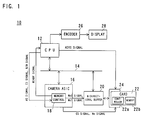
- an image reproducing apparatus 10 of this embodiment includes a CPU 12 of a synchronous bus scheme.
- the CPU 12 is connected, through a data bus 14, with a camera ASIC 16 and a bi-directional buffer 20.
- a memory card 22 when received in a slot 24 is put into connection to the bi-directional buffer 20.
- the memory card 22 has a controller 22a and a memory 22b, so that the controller 22a is connected to the bi-directional buffer 20. Consequently, access to the memory 22b is through the controller 22a.
- the memory card 22 is a removable recording medium, such as a compact flash, compatible with the PCMCIA format.
- the CPU 12 When reading data from the memory card 22, the CPU 12 outputs an address strobe signal (AS signal), a chip select signal (CS signal), an R/W signal for identifying an access content and an address signal (ADRS signal).
- AS signal address strobe signal
- CS signal chip select signal
- ADRS signal address signal
- the AS signal, CS signal and R/W signal is supplied to a memory control circuit 18 provided in the camera ASIC 16 while the ADRS signal is given to the memory card 22.
- the memory control circuit 18 supplies a control signal (Wc0 signal, Wcl signal) to the bi-directional buffer 20, and further CS signal and output enable signal (We signal) to the memory card 22. Due to this, data is read from a desired address of the memory 22b. The read-out data is outputted onto the bi-directional buffer 20 and, through the bus 14, to the CPU 12.
- the CPU 12 provides this image data to a display 28 through an encoder 26. As a result, a reproduced image is displayed on the screen of the display 28.
- the data to be read from the memory 22b includes, besides image data, capacity value data representative of a capacity value of the memory 22b.
- the CPU 12 prior to reading out image data, reads out capacity value data. According to a value of the read capacity data, the CPU 12 switches its own access processing period and an access processing period for the memory control circuit 18. That is, if the memory 22b is in large capacity, the access processing period is shortened while, if the memory 22b is in small capacity, the access processing period is increased.
- step S1 it is determined in step S1 whether a memory card 22 is inserted in the slot 24 or not.
- step S3 the capacity value data of the memory 22b is read from the memory card 22.
- step S5 the capacity value represented by the capacity value data is compared with a predetermined threshold. If the capacity value is in excess of the threshold, in step S7 a short-time access mode is set to itself and to the memory control circuit 18. If the capacity value is below the threshold, in step S9 a long-time access mode is set to itself and the memory control circuit 18. After completing the mode setting, in step S11 an image-data reproducing process is executed.
- step S7 or S9 image data is read from the memory card 22 according to the mode as established in the step S7 or S9.
- the CPU 12 advances to step S13 each time the reproducing process completes once, to thereby determine whether the memory card 22 has been removed from the slot 26 or not. If “NO”, the process returns to the step S11. However, if "YES”, the process is ended.
- the access-mode set process is made upon inserting the memory card 22.
- the access mode is not again established unless the memory card 22 is removed.
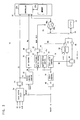
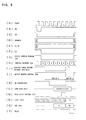
- the memory control circuit 18, in concrete, is configured as shown in Figure 3. Meanwhile, when reading capacity value data from the memory card 22 or when image data is read from the memory card 22 in the long-time access mode, the CPU 12 and the memory control circuit 18 operate in timing as shown in Figure 4.
- the AS, CS, ADRS and R/W signals are outputted from the CPU 12, in timing as shown in Figure 4(B) to Figure 4(E). Both the AS signal and the CS signal are active-low signals.
- An access start circuit 24 receives R/W, AS and CS signals and outputs a CS signal shown in Figure 4(F) and an access control window signal (Wa signal) shown in Figure 4(G).
- the CS and Wa signals are also active-low signals, which are synchronized with a clock as shown in Figure 4(A) by a latch circuit 26.
- the CS signal is provided to the controller 22a, while the Wa signal is to a counter 28 for access control. This makes active the controller 22a and counter 28.
- the destination address of reading the memory 22b is specified by an ADRS signal directly given from the CPU 12.
- the count value (Wb signal) of the counter 28 is incremented responsive to the clock as shown in Figure 4(H).
- the count value like this is provided to an OE control circuit 30, a bi-directional buffer control circuit 32, an output buffer control circuit 34, a data latch control circuit 36 and a READY control circuit 38.
- the OE control circuit 30 generates an output enable signal (We signal) when the count value takes "1" - "5".
- the We signal is outputted through the latch circuit 40, in timing as shown in Figure 4(K).
- the bi-directional buffer control circuit 32 generates control signals (Wc0 signal, Wcl signal) when the count value takes "0" - "5". These control signals are outputted, through the latch circuit 42, in timing as shown in Figure 4(I).
- the output buffer control circuit generates a control signal (Wd signal) when the count value takes “6” - “7". This Wd signal is outputted in timing as shown in Figure 4(J). Furthermore, the data latch control circuit 36, when the count value takes “6”, generates a control signal (Wf signal) as shown in Figure 4(M). Also, the READY control circuit 38 generates a ready signal when the count value takes "7”. The READY signal is outputted, through the latch circuit 46, in timing as shown in Figure 4(P).
- the Wc0 signal, the Wcl signal, the Wd signal, the We signal and the READY signal as active low signals are delayed by in the latch circuits 40 - 46.
- the active-high Wf signal is outputted as it is without delay.
- the We signal outputted from the latch circuit 40 is provided to the controller 22a.
- the controller 22a in a period that signal assumes a low level reads data from the memory 22b.
- the data is held in an extremely short period even after a rise in the We signal, and data reading timing is expressed as shown in Figure 4(L).
- the Wc0 and Wcl signals outputted from the latch circuit 42 are provided to the bi-directional buffer 20.
- the bi-directional buffer 20 is powered on by the Wc0 signal.
- the buffer 20a is disabled and the buffer 20b is enabled by the Wcl signal. Consequently, only in the period A shown in Figure 4, data transfer is possible from the memory card 22 toward the data bus 14.
- the read data (data Da) is passed through the bi-directional buffer 20 and data bus 14 and inputted to the memory control circuit 18, in timing as shown in Figure 4(O).
- the data Da is passed through the buffer 48 and supplied to the latch circuit 50 where it is latched by a rise of the clock in a period the Wf signal outputted from the data latch control circuit 36 is in rise. That is, the data Da is latched at a time that the count value becomes "7".
- the latch data is Db
- the data Db is outputted from the latch circuit 50 in timing shown in Figure 4(N), and inputted to the buffer 54 through a select circuit 52.
- the buffer 54 is enabled in a period B shown in Figure 4 by a Wd signal outputted from the latch circuit 44, and outputs data Db on to the data bus 14 only in the period B. As a result, the data transferred over the data bus 14 is switched from Da into Db, in timing shown in Figure 4(O).
- a READY signal is outputted when the count value becomes "8".
- the READY signal is supplied to the access start circuit 24 and the counter 28, besides to the CPU 12.
- the access start circuit 24 is disabled at a rise in the READY signal. This suspends the CS and Wa signals from outputting.
- the counter 28 is reset at a rise in the READY signal.
- controller 22a is disabled two clocks after the data Da has been latched.
- the CPU fetches the data Db at a rise in the clock during an input period of the READY signal, and suspends the AS, CS, R/W and ADRS signals from being outputted at a rise in the READY signal.
- the AS, CS, ADRS and R/W signals are outputted from the CPU 12 in timing as shown in Figure 5(B) to Figure 5(E).
- the access start circuit 24 outputs a CS signal shown in Figure 5(F) and an access control window signal (Wa signal) shown in Figure 5(G), in response to a rise in the AS signal.
- the output CS and Wa signals are latched in the latch circuit 26.
- the CS signal is supplied to the controller 22 while the Wa signal to the counter 28.
- the count value (Wb signal) of the counter 28 is incremented responsive to the clock as shown in Figure 5(H).
- the OE control circuit 30 generates an output enable signal (We signal) when the counter 28 takes a count value of "1" - "3".
- the We signal is outputted through the latch circuit 40 in timing as shown in Figure 5(K).
- the bi-directional buffer control circuit 32 generates a control signal (Wc0 signal, Wcl signal) when the count value takes "0" - "3". These signals are also outputted through the latch circuit 42, in timing as shown in Figure 5(I).
- the output buffer control circuit 34 generates a control signal (Wd signal) when the count value takes "4" - "5".
- This Wd signal is also outputted in timing as shown in Figure 5(J). Furthermore, the data latch control circuit 36 generates a control signal (Wf signal) shown in Figure 5(M) when the count value takes "4". The READY control circuit 38 generates a READY signal and the count value takes "5". This READY signal is outputted through the latch circuit 46 in timing as shown in Figure 5(P).
- the We signal outputted from the latch circuit 40 is supplied to the controller 22a so that the controller 22a reads data from the memory 22b in a period the We signal takes a low level.
- the data is held in a slight period even after a rise in the We signal, wherein the timing of reading out the data is as shown in Figure 5(L).
- the Wc0 and Wc1 signals outputted from the latch circuit 42 are supplied to the bi-directional buffer 20 so that data transfer is made possible from the memory card 22 toward the data bus 14 only in a period A shown in Figure 5. Consequently, the data read out of the memory 22b (data Da) is inputted to the memory control circuit 18 through the bi-directional buffer 20 and data bus 14, in timing as shown in Figure 5(O).
- the data Da is supplied to the latch circuit 50 through the buffer 48, where it is latched at a rise of the clock during a period the Wf signal outputted from the data latch control circuit 36 rises. That is, the data Da is latched at a time point that the count value becomes "5".
- the latch data Db is outputted from the latch circuit in timing shown in Figure 5(N) and inputted to the buffer through the select circuit 52.
- the buffer 54 is enabled in the period shown in Figure 5 by the Wd signal outputted from the latch circuit 44, and outputs data Db onto the data bus 14 only in this period B. As a result, the data transferred over the data bus 14 is switched from Da to Db in timing shown in Figure 5(O).
- a READY signal is outputted from the latch circuit 46 and supplied to the CPU 12, the access start circuit 24 and the counter 28.
- the access start circuit 24 suspends CS and Wa signals from outputting at a rise in the READY signal.
- the counter 28 is reset at the rise in the READY signal.
- the CPU 12 fetches the data Db in the clock rise during the period of inputting the READY signal, and suspends the AS, CS, R/W and ADRS signals from being outputted at the rise in the READY signal.
- the various access control signals outputted from the CPU 12 and memory control circuit 18 have active periods shorter in the brief-time access mode than in the long-time access mode.
- the brief-time access mode herein is established when the capacity of the memory 22b is greater than a predetermined threshold. This is due to the consideration that the greater the capacity value of the memory 22b the higher the performance of the controller 22a becomes wherein the controller 22a can positively access a desired address even if the active period of the access control signal is brief. As a result, the controller 22a is allowed to exhibit its performance to a maximum extent, and access is at a higher speed as the capacity of the memory 22b is increased.
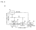
- FIG. 6 another embodiment of a data processing apparatus 10 is configured similar to the image reproducing apparatus 10 shown in Figure 1, except in that the encoder 26 and display 28 is omitted. Hence, duplicated explanation on the similar portions will be omitted.
- the CPU 12 When reading data out of the memory card 22, the CPU 12 outputs AS, CS, R/W and ADRS signals. Among these, the AS, CS and R/W signals are supplied to the memory control circuit 18 provided in the camera ASIC 16 while the ADRS signal is to the memory card 22.
- the memory control circuit 18, in response to the input signals, delivers Wc0 and Wcl signals to the bi-directional buffer 20 and further CS and We signals to the memory card 22. Due to this, a data signal is read from a desired address of the memory 22b and the read data signal is outputted to the CPU 12 through the bi-directional buffer 20 and bus 14.
- the camera ASIC 16 outputs, by itself, a READY signal to the CPU 12 in timing the data signal is supplied to the CPU 12.
- the CPU 12 concretely processes a flowchart shown in Figure 7.
- step S21 it is determined in step S21 whether the memory card 22 is inserted in the slot 24 or not. If not inserted, in step S23 an alert is generated. On the other hand, if the memory card 22 is received, in step S25 the access time is set to a maximum value. Specifically, the active periods of the CS, R/W and ADRS signals to be outputted, by itself, are set to maximum values, and further a control signal is provided to the camera ASIC 16 to set the active periods of the Wc0, Wc1, CS and We signals to maximum values.
- step S27 AS and CS signals and an R/W signal representative of "reading out” are supplied to the camera ASIC 16, and further an ADRS signal representative of a storage address of an ID data signal is given to the memory card 22.
- the controller 22a provided on the memory card 22 is supplied with the CS, We and ADRS signals set with the active periods at maxim values. Due to this, an ID data signal is read from the ID storage address of the memory 22b.
- step S29 a capacity value of the memory 22b is detected from the read ID data signal. That is, the ID data signal has common data, such as type number, that is common to any memory card and capacity value data representative of a capacity value.
- a capacity value data is detected from the ID data signal.
- step S31 it is determined based on detected capacity value data whether the capacity value of the memory 22b is greater than a predetermined value (e.g. 8 M bytes) or not. If the capacity value ⁇ the predetermined value, the process directly enters an access process to a desired data signal of step S43. That is, by the determination of "NO" in the step S31, the maximum active period (maximum access time) is determined as an optimal active period (optimal access time). As a result, in the step S43 the memory card 22 is given the CS, We and ADRS signals assuming the maximums in the active periods whereby an access process is made with the maximum access time.
- a predetermined value e.g. 8 M bytes
- step S33 the access time is reduced by one step. That is, the active periods of the CS, R/W and ADRS signals to be outputted by itself and the active periods of the Wc0, Wc1, CS and We signals to be outputted from the memory control circuit 18 are set to periods shorter by one step than those in the present time.
- step S35 the memory card 22 is accessed with various signals set again with active periods in a manner similar to the step S27, to read an ID data signal out of the memory 22b.
- step S37 common data is detected from the read ID data signal.
- step S39 a detected common data value is compared with a predetermined value, to determine whether the ID data signal is proper or not. If the common data value herein represents a predetermined value, the ID data signal is considered having been properly read out (considered the ID data signal as proper) and the process returns to the step S33. As a result of returning to the step S33, the access time is reduced further by one step, and an ID data signal is again read out with a reduced access time.
- step S39 If an ID data signal is not properly read out because of shortening the access time and a common-data value shows a different value form the predetermined value, then "NO" is determined (the read ID data signal is improper) in step S39.
- the access time is increased by one step in step S41. That is, the active periods of CS, R/W and ADRS signals to be outputted by the own and the active periods of Wc0, Wcl, CS and We signals to be outputted from the memory control circuit 18 are set to the shortest periods for properly reading out an ID data signal. This makes it possible to determine, as an optimal active period, a shortest active period for properly reading out an ID data signal. After determining the optimal active period, in step S43 an access process to a desired data signal is executed.
- the memory control circuit 18 is configured similarly to that of the first embodiment (i.e., as shown in Figure 3).
- the CPU 12 and the memory control circuit 18 operate in timing as shown in Figure 8.
- the access time is reduced by one step
- the CPU 12 and the memory control circuit 18 operate in timing as shown in Figure 9.
- the CPU 12 and the memory control circuit 18 operate in timing as shown in Figure 10.
- the timing charts shown in Figure 8 to Figure 10 are almost similar to the timing charts shown in Figure 4 and Figure 5, hence omitting concrete explanation.
- the Wb signal (count value) is incremented from “0" to "8".
- the Wc0 and Wc1 signals shown in Figure 8(I) are active when the count value takes “1” - “6".
- the Wd signal shown in Figure 8(J) is active when the count value takes "7” or "8".
- the We signal shown in Figure 8(K) is active when the count value takes "2" - "6".
- the Wf signal shown in Figure 8(M) is active when the count value takes "6” while the READY signal shown in Figure 8(P) is active when the count value takes "8".
- the Wb signal is incremented from “0" to "7" ( Figure 9(H)).
- the Wc0 and Wc1 signals are active when the count value is “1" - "5" ( Figure 9(I)).
- the Wd signal is active when the count value takes “6” or “7” ( Figure 9(J)).
- the We signal is active when the count value takes "2"-"5" ( Figure 9(K)).
- the Wf signal is active in the count value takes "5" ( Figure 9(M)) while the READY signal is active when the count value takes "7” ( Figure 9(P)).
- the Wb signal is incremented from “0" to "6" ( Figure 10(H)).
- the Wc0 and Wcl signals are active when the count value takes “1" - "4" ( Figure 10(I)).
- the Wd signal is active when the count value takes “5" or “6” ( Figure 10(J)).
- the We signal is active when the count value takes “2" - "4" ( Figure 10(K)).
- the Wf signal is active when the count value takes "4" ( Figure 10(M)).
- the READY signal is active when the count value takes "6" ( Figure 10(P)).
- the controller when reading data signals from the memory card 22 held in the slot 24, first the ADRS, CS and We signals in the maximum active periods are supplied to the controller, and an ID data signal is read from an ID storage address of the memory 22b.
- This ID data signal contains the data of a capacity value (total capacity value) of the memory. With this capacity value data, it is determined whether the memory capacity is greater than a predetermined value or not. If the capacity value is less than the predetermined value, the maximum active period is determined as an optimal active period. That is, the maximum active period is made effective.
- an ID data signal is read from the memory according to the ADRS, CS and We signals different in active period from one another.
- the read ID data signals are determined as to whether proper or not. Specifically, the common data contained in the ID data is compared to a predetermined value. If the common data in value shows a predetermined value, the ID data signal is determined proper. However, if the common data value does not show the predetermined value, the ID data signal is determined improper.
- the shortest active period among the active periods that the ID data signal determined proper has been read out is determined as an optimal active period. That is, the shortest active period that the ID data signal has been properly read out is made effective.
- the controller can exhibit the function to a maximum.
- the active period when determining a shortest active period for properly reading out an ID data signal, the active period is shortened by one step per time.
- the shortest active period may be determined by rather extending the active period by one step per time.
- the common data contained in the ID data signal is read out and the common data value is compared with a predetermined value, thereby determining as to whether the ID data signal is proper or not.
- the properness of the ID data signal may be determined by the capacity value data read out prior to the common data.
- the capacity value data read out with the maximum access time may be held in a register so that various ones of capacity value data read out with different ones of access time are compared with the capacity value data in the register.
- a memory stick produced by Sony
- a disk recording medium such as a micro-drive (produced by IBM) may be employed.
- the control signals Wc0, Wc1, Wd, We, Wf and READY signals were controlled in output timing by the counter, a state machine other than the counter may be used in controlling the timing.
- this invention is also effective for write operation.
Landscapes
- Engineering & Computer Science (AREA)
- Theoretical Computer Science (AREA)
- Physics & Mathematics (AREA)
- General Engineering & Computer Science (AREA)
- General Physics & Mathematics (AREA)
- Television Signal Processing For Recording (AREA)
- Read Only Memory (AREA)
- Credit Cards Or The Like (AREA)
Applications Claiming Priority (4)
| Application Number | Priority Date | Filing Date | Title |
|---|---|---|---|
| JP2000035058 | 2000-02-14 | ||
| JP2000035058A JP3495675B2 (ja) | 2000-02-14 | 2000-02-14 | メモリアクセス回路 |
| JP2000137508A JP3691340B2 (ja) | 2000-05-10 | 2000-05-10 | メモリアクセス制御回路 |
| JP2000137508 | 2000-05-10 |
Publications (3)
| Publication Number | Publication Date |
|---|---|
| EP1130521A2 true EP1130521A2 (de) | 2001-09-05 |
| EP1130521A3 EP1130521A3 (de) | 2006-04-19 |
| EP1130521B1 EP1130521B1 (de) | 2008-02-13 |
Family
ID=26585291
Family Applications (1)
| Application Number | Title | Priority Date | Filing Date |
|---|---|---|---|
| EP01103332A Expired - Lifetime EP1130521B1 (de) | 2000-02-14 | 2001-02-13 | Speicherzugriffschaltung und Speicherzugriffsteuerungsschaltung |
Country Status (4)
| Country | Link |
|---|---|
| US (2) | US6578125B2 (de) |
| EP (1) | EP1130521B1 (de) |
| KR (1) | KR100787710B1 (de) |
| DE (1) | DE60132726T2 (de) |
Cited By (1)
| Publication number | Priority date | Publication date | Assignee | Title |
|---|---|---|---|---|
| WO2003074024A1 (en) | 2002-03-01 | 2003-09-12 | Chiesi Farmaceutici S.P.A | Formoterol superfine formulation |
Families Citing this family (19)
| Publication number | Priority date | Publication date | Assignee | Title |
|---|---|---|---|---|
| US7295443B2 (en) | 2000-07-06 | 2007-11-13 | Onspec Electronic, Inc. | Smartconnect universal flash media card adapters |
| US6832281B2 (en) * | 2000-07-06 | 2004-12-14 | Onspec Electronic Inc. | Flashtoaster for reading several types of flash memory cards with or without a PC |
| US7278051B2 (en) * | 2000-07-06 | 2007-10-02 | Onspec Electronic, Inc. | Field-operable, stand-alone apparatus for media recovery and regeneration |
| US7252240B1 (en) * | 2000-07-06 | 2007-08-07 | Onspec Electronics, Inc. | Memory module which includes a form factor connector |
| US6438638B1 (en) * | 2000-07-06 | 2002-08-20 | Onspec Electronic, Inc. | Flashtoaster for reading several types of flash-memory cards with or without a PC |
| JPWO2002069127A1 (ja) * | 2001-02-26 | 2004-07-02 | 東京エレクトロンデバイス株式会社 | 記憶媒体制御方法、記憶媒体制御装置、および記憶媒体アダプタ |
| US6711640B1 (en) * | 2001-03-29 | 2004-03-23 | Intel Corporation | Split delay transmission line |
| US7162549B2 (en) | 2001-10-29 | 2007-01-09 | Onspec Electronics, Inc. | Multimode controller for intelligent and “dumb” flash cards |
| US6944738B2 (en) * | 2002-04-16 | 2005-09-13 | Sun Microsystems, Inc. | Scalable design for DDR SDRAM buses |
| JP2006031339A (ja) * | 2004-07-15 | 2006-02-02 | Sanyo Electric Co Ltd | フォーマット処理装置および処理方法 |
| US7427027B2 (en) | 2004-07-28 | 2008-09-23 | Sandisk Corporation | Optimized non-volatile storage systems |
| US7899990B2 (en) * | 2005-11-15 | 2011-03-01 | Oracle America, Inc. | Power conservation via DRAM access |
| US7934054B1 (en) | 2005-11-15 | 2011-04-26 | Oracle America, Inc. | Re-fetching cache memory enabling alternative operational modes |
| US7958312B2 (en) * | 2005-11-15 | 2011-06-07 | Oracle America, Inc. | Small and power-efficient cache that can provide data for background DMA devices while the processor is in a low-power state |
| US7516274B2 (en) * | 2005-11-15 | 2009-04-07 | Sun Microsystems, Inc. | Power conservation via DRAM access reduction |
| KR20080004773A (ko) * | 2006-07-06 | 2008-01-10 | 삼성전자주식회사 | 하드 디스크의 액세스 타임 자동 설정 방법 및 그 장치 |
| US8370911B1 (en) * | 2008-11-20 | 2013-02-05 | George Mallard | System for integrating multiple access controls systems |
| US20130151755A1 (en) | 2011-12-12 | 2013-06-13 | Reuven Elhamias | Non-Volatile Storage Systems with Go To Sleep Adaption |
| US9411721B2 (en) | 2013-11-15 | 2016-08-09 | Sandisk Technologies Llc | Detecting access sequences for data compression on non-volatile memory devices |
Citations (6)
| Publication number | Priority date | Publication date | Assignee | Title |
|---|---|---|---|---|
| EP0534883A1 (de) * | 1991-09-16 | 1993-03-31 | International Business Machines Corporation | Verfahren und Gerät zur Synchronisierung der Auslese einer sequentiellen Mediumvorrichtung mit einer getrennten taktgesteuerten Vorrichtung |
| EP0709786A1 (de) * | 1994-10-25 | 1996-05-01 | Oki Electric Industry Co., Ltd. | Halbleiterspeicher mit Synchronisationssteuerung zum Empfang von Daten in einem Ziel-Halbleiterspeichermodul |
| US5604917A (en) * | 1990-09-28 | 1997-02-18 | Fuji Photo Film Co., Ltd. | IC memory card having masking function for preventing writing of data into a fixed memory area |
| EP0831402A1 (de) * | 1996-09-23 | 1998-03-25 | Hewlett-Packard Company | Dynamisches Konfigurieren des Zeitverhaltens zur Anpassung an Speicherbuslastbedingungen |
| EP0855653A1 (de) * | 1997-01-23 | 1998-07-29 | Hewlett-Packard Company | Speichersteuerungsvorrichtung mit programmierbarer Impulsverzögerung |
| US5946712A (en) * | 1997-06-04 | 1999-08-31 | Oak Technology, Inc. | Apparatus and method for reading data from synchronous memory |
Family Cites Families (3)
| Publication number | Priority date | Publication date | Assignee | Title |
|---|---|---|---|---|
| JPH04192047A (ja) * | 1990-11-27 | 1992-07-10 | Toshiba Corp | パーソナルコンピュータ |
| JPH07105101A (ja) * | 1993-09-30 | 1995-04-21 | Toshiba Corp | メモリモジュールまたはメモリカード |
| JPH10233986A (ja) | 1997-02-21 | 1998-09-02 | Hitachi Ltd | 映像信号記録装置 |
-
2001
- 2001-02-12 US US09/780,424 patent/US6578125B2/en not_active Expired - Fee Related
- 2001-02-13 EP EP01103332A patent/EP1130521B1/de not_active Expired - Lifetime
- 2001-02-13 DE DE60132726T patent/DE60132726T2/de not_active Expired - Lifetime
- 2001-02-14 KR KR1020010007201A patent/KR100787710B1/ko not_active IP Right Cessation
-
2003
- 2003-02-28 US US10/375,000 patent/US6742095B2/en not_active Expired - Fee Related
Patent Citations (6)
| Publication number | Priority date | Publication date | Assignee | Title |
|---|---|---|---|---|
| US5604917A (en) * | 1990-09-28 | 1997-02-18 | Fuji Photo Film Co., Ltd. | IC memory card having masking function for preventing writing of data into a fixed memory area |
| EP0534883A1 (de) * | 1991-09-16 | 1993-03-31 | International Business Machines Corporation | Verfahren und Gerät zur Synchronisierung der Auslese einer sequentiellen Mediumvorrichtung mit einer getrennten taktgesteuerten Vorrichtung |
| EP0709786A1 (de) * | 1994-10-25 | 1996-05-01 | Oki Electric Industry Co., Ltd. | Halbleiterspeicher mit Synchronisationssteuerung zum Empfang von Daten in einem Ziel-Halbleiterspeichermodul |
| EP0831402A1 (de) * | 1996-09-23 | 1998-03-25 | Hewlett-Packard Company | Dynamisches Konfigurieren des Zeitverhaltens zur Anpassung an Speicherbuslastbedingungen |
| EP0855653A1 (de) * | 1997-01-23 | 1998-07-29 | Hewlett-Packard Company | Speichersteuerungsvorrichtung mit programmierbarer Impulsverzögerung |
| US5946712A (en) * | 1997-06-04 | 1999-08-31 | Oak Technology, Inc. | Apparatus and method for reading data from synchronous memory |
Cited By (2)
| Publication number | Priority date | Publication date | Assignee | Title |
|---|---|---|---|---|
| WO2003074024A1 (en) | 2002-03-01 | 2003-09-12 | Chiesi Farmaceutici S.P.A | Formoterol superfine formulation |
| EP2201964A2 (de) | 2002-03-01 | 2010-06-30 | CHIESI FARMACEUTICI S.p.A. | Extra feine Formoterol-Formulierung |
Also Published As
| Publication number | Publication date |
|---|---|
| DE60132726D1 (de) | 2008-03-27 |
| DE60132726T2 (de) | 2009-03-05 |
| US20030131208A1 (en) | 2003-07-10 |
| KR20010082617A (ko) | 2001-08-30 |
| US6742095B2 (en) | 2004-05-25 |
| EP1130521B1 (de) | 2008-02-13 |
| US6578125B2 (en) | 2003-06-10 |
| KR100787710B1 (ko) | 2007-12-21 |
| US20010014934A1 (en) | 2001-08-16 |
| EP1130521A3 (de) | 2006-04-19 |
Similar Documents
| Publication | Publication Date | Title |
|---|---|---|
| EP1130521B1 (de) | Speicherzugriffschaltung und Speicherzugriffsteuerungsschaltung | |
| US7478260B2 (en) | System and method for setting a clock rate in a memory card | |
| JPS61125641A (ja) | デ−タ圧縮制御方式 | |
| KR100319331B1 (ko) | 버스제어장치및버스제어방법 | |
| JPH04165866A (ja) | バッファメモリ回路 | |
| CN108632552A (zh) | 记录装置、控制方法和存储介质 | |
| KR20030035906A (ko) | 기록장치 | |
| US10545680B2 (en) | Recording/reproduction apparatus, control method of recording/reproduction apparatus, and non-transitory computer-readable storage medium | |
| US6584512B1 (en) | Communication DMA device for freeing the data bus from the CPU and outputting divided data | |
| JP2003036202A (ja) | 記憶装置 | |
| EP0334552B1 (de) | Halbleiterdateispeicher und Speichersystem mit Anwendung dieses Speichers | |
| US7198191B2 (en) | Signal processing apparatus for recording or playing back data | |
| JP3691340B2 (ja) | メモリアクセス制御回路 | |
| JP3495675B2 (ja) | メモリアクセス回路 | |
| JP2001101356A (ja) | 表示機能付きメモリカードアダプタ | |
| JP3820682B2 (ja) | メモリ制御装置、データ書き込み読み出し方法、及び撮像装置 | |
| JP2001184302A (ja) | バッファ制御回路 | |
| JP3481156B2 (ja) | データ読み出し回路 | |
| JP2594678B2 (ja) | システム制御装置 | |
| JP3568384B2 (ja) | メモリアクセス回路 | |
| JP3509658B2 (ja) | 動作モード切替え回路及びその方法 | |
| JPS63267060A (ja) | 画情報バツフア制御方法 | |
| JPH11120757A (ja) | Fifoレジスタ回路 | |
| JPH07253920A (ja) | Fifo ram コントローラ | |
| JP2019109557A (ja) | 半導体記憶装置及び画像処理装置 |
Legal Events
| Date | Code | Title | Description |
|---|---|---|---|
| PUAI | Public reference made under article 153(3) epc to a published international application that has entered the european phase |
Free format text: ORIGINAL CODE: 0009012 |
|
| AK | Designated contracting states |
Kind code of ref document: A2 Designated state(s): AT BE CH CY DE DK ES FI FR GB GR IE IT LI LU MC NL PT SE TR |
|
| AX | Request for extension of the european patent |
Free format text: AL;LT;LV;MK;RO;SI |
|
| PUAL | Search report despatched |
Free format text: ORIGINAL CODE: 0009013 |
|
| AK | Designated contracting states |
Kind code of ref document: A3 Designated state(s): AT BE CH CY DE DK ES FI FR GB GR IE IT LI LU MC NL PT SE TR |
|
| AX | Request for extension of the european patent |
Extension state: AL LT LV MK RO SI |
|
| 17P | Request for examination filed |
Effective date: 20060628 |
|
| 17Q | First examination report despatched |
Effective date: 20060905 |
|
| AKX | Designation fees paid |
Designated state(s): DE FR GB |
|
| GRAP | Despatch of communication of intention to grant a patent |
Free format text: ORIGINAL CODE: EPIDOSNIGR1 |
|
| GRAS | Grant fee paid |
Free format text: ORIGINAL CODE: EPIDOSNIGR3 |
|
| GRAA | (expected) grant |
Free format text: ORIGINAL CODE: 0009210 |
|
| AK | Designated contracting states |
Kind code of ref document: B1 Designated state(s): DE FR GB |
|
| REG | Reference to a national code |
Ref country code: GB Ref legal event code: FG4D |
|
| REF | Corresponds to: |
Ref document number: 60132726 Country of ref document: DE Date of ref document: 20080327 Kind code of ref document: P |
|
| EN | Fr: translation not filed | ||
| PLBE | No opposition filed within time limit |
Free format text: ORIGINAL CODE: 0009261 |
|
| STAA | Information on the status of an ep patent application or granted ep patent |
Free format text: STATUS: NO OPPOSITION FILED WITHIN TIME LIMIT |
|
| 26N | No opposition filed |
Effective date: 20081114 |
|
| PG25 | Lapsed in a contracting state [announced via postgrant information from national office to epo] |
Ref country code: FR Free format text: LAPSE BECAUSE OF FAILURE TO SUBMIT A TRANSLATION OF THE DESCRIPTION OR TO PAY THE FEE WITHIN THE PRESCRIBED TIME-LIMIT Effective date: 20081205 |
|
| REG | Reference to a national code |
Ref country code: DE Ref legal event code: R082 Ref document number: 60132726 Country of ref document: DE Representative=s name: GLAWE DELFS MOLL PARTNERSCHAFT MBB VON PATENT-, DE |
|
| REG | Reference to a national code |
Ref country code: DE Ref legal event code: R081 Ref document number: 60132726 Country of ref document: DE Owner name: XACTI CORP., JP Free format text: FORMER OWNER: SANYO ELECTRIC CO., LTD., MORIGUCHI-SHI, JP Effective date: 20140520 Ref country code: DE Ref legal event code: R082 Ref document number: 60132726 Country of ref document: DE Representative=s name: GLAWE DELFS MOLL PARTNERSCHAFT MBB VON PATENT-, DE Effective date: 20140520 Ref country code: DE Ref legal event code: R081 Ref document number: 60132726 Country of ref document: DE Owner name: XACTI CORP., JP Free format text: FORMER OWNER: SANYO ELECTRIC CO., LTD., MORIGUCHI-SHI, OSAKA, JP Effective date: 20140520 |
|
| PGFP | Annual fee paid to national office [announced via postgrant information from national office to epo] |
Ref country code: GB Payment date: 20140212 Year of fee payment: 14 |
|
| PGFP | Annual fee paid to national office [announced via postgrant information from national office to epo] |
Ref country code: DE Payment date: 20140417 Year of fee payment: 14 |
|
| REG | Reference to a national code |
Ref country code: GB Ref legal event code: 732E Free format text: REGISTERED BETWEEN 20140821 AND 20140827 |
|
| REG | Reference to a national code |
Ref country code: DE Ref legal event code: R119 Ref document number: 60132726 Country of ref document: DE |
|
| GBPC | Gb: european patent ceased through non-payment of renewal fee |
Effective date: 20150213 |
|
| PG25 | Lapsed in a contracting state [announced via postgrant information from national office to epo] |
Ref country code: DE Free format text: LAPSE BECAUSE OF NON-PAYMENT OF DUE FEES Effective date: 20150901 Ref country code: GB Free format text: LAPSE BECAUSE OF NON-PAYMENT OF DUE FEES Effective date: 20150213 |