EP1118878A1 - Szintillatorpanel, strahlungsbildsensor und verfahren zu deren herstellung - Google Patents
Szintillatorpanel, strahlungsbildsensor und verfahren zu deren herstellung Download PDFInfo
- Publication number
- EP1118878A1 EP1118878A1 EP99925377A EP99925377A EP1118878A1 EP 1118878 A1 EP1118878 A1 EP 1118878A1 EP 99925377 A EP99925377 A EP 99925377A EP 99925377 A EP99925377 A EP 99925377A EP 1118878 A1 EP1118878 A1 EP 1118878A1
- Authority
- EP
- European Patent Office
- Prior art keywords
- scintillator
- film
- flat resin
- substrate
- image sensor
- Prior art date
- Legal status (The legal status is an assumption and is not a legal conclusion. Google has not performed a legal analysis and makes no representation as to the accuracy of the status listed.)
- Granted
Links
Images


Classifications
-
- G—PHYSICS
- G01—MEASURING; TESTING
- G01T—MEASUREMENT OF NUCLEAR OR X-RADIATION
- G01T1/00—Measuring X-radiation, gamma radiation, corpuscular radiation, or cosmic radiation
- G01T1/16—Measuring radiation intensity
- G01T1/20—Measuring radiation intensity with scintillation detectors
-
- G—PHYSICS
- G21—NUCLEAR PHYSICS; NUCLEAR ENGINEERING
- G21K—HANDLING OF PARTICLES OR IONISING RADIATION NOT OTHERWISE PROVIDED FOR; IRRADIATION DEVICES; GAMMA RAY OR X-RAY MICROSCOPES
- G21K4/00—Conversion screens for the conversion of the spatial distribution of X-rays or particle radiation into visible images, e.g. fluoroscopic screens
-
- G—PHYSICS
- G01—MEASURING; TESTING
- G01T—MEASUREMENT OF NUCLEAR OR X-RADIATION
- G01T1/00—Measuring X-radiation, gamma radiation, corpuscular radiation, or cosmic radiation
- G01T1/16—Measuring radiation intensity
- G01T1/20—Measuring radiation intensity with scintillation detectors
- G01T1/202—Measuring radiation intensity with scintillation detectors the detector being a crystal
-
- G—PHYSICS
- G03—PHOTOGRAPHY; CINEMATOGRAPHY; ANALOGOUS TECHNIQUES USING WAVES OTHER THAN OPTICAL WAVES; ELECTROGRAPHY; HOLOGRAPHY
- G03B—APPARATUS OR ARRANGEMENTS FOR TAKING PHOTOGRAPHS OR FOR PROJECTING OR VIEWING THEM; APPARATUS OR ARRANGEMENTS EMPLOYING ANALOGOUS TECHNIQUES USING WAVES OTHER THAN OPTICAL WAVES; ACCESSORIES THEREFOR
- G03B42/00—Obtaining records using waves other than optical waves; Visualisation of such records by using optical means
- G03B42/02—Obtaining records using waves other than optical waves; Visualisation of such records by using optical means using X-rays
Definitions
- the present invention relates to a scintillator panel and a radiation image sensor which are used for medical X-ray photography and the like, and methods of making them.
- X-ray sensitive films have been used in medical and industrial X-ray photography
- radiation imaging systems using radiation detectors have been coming into wider use from the viewpoint of convenience and their storability of photographed results.
- pixel data caused by two-dimensional radiation are acquired by a radiation detector as an electric signal, which is then processed by a processing unit, so as to be displayed onto a monitor.
- a typical radiation detector is one disclosed in WO92/06476 or the like.
- a scintillator directly formed on a substrate and an imaging device are bonded together, such that the radiation incident from the substrate side is converted into visible light by the scintillator, so as to be detected.
- Japanese Patent Application Laid-Open No. HEI 5-196742 and No. SHO 63-215987 disclose a radiation detector in which, in order to protect a scintillator formed on an imaging device or a fiber optical plate (FOP), i.e., an optical part constituted by a plurality of fibers bundled together, against vapor (moisture) in the air, a water-impermeable, moisture-resistant barrier is formed on the upper side of scintillator layer.
- FOP fiber optical plate
- the state of substrate surface (such as unevenness, roughness, and streaks formed upon rolling) has greatly influenced characteristics of scintillator panels. Namely, optical mirror surfaces are hard to prepare in Al sheets, Be sheets, and the like which are used as substrates. Therefore, in the case where radiation is made incident from the substrate side and is converted by the scintillator into visible light, from which an image is subsequently acquired through lens coupling and the like, image quality, luminance, resolution, and the like have greatly been influenced by the state of substrate surface.
- the scintillator panel of the present invention comprises a radiation-transparent substrate, a flat resin film formed on the substrate, a reflecting film formed on the flat resin film, and a scintillator formed on the reflecting film. According to the scintillator panel of the present invention, since the scintillator is provided on the flat resin film formed on the substrate, characteristics of the scintillator panel can be kept from changing due to the state of substrate surface. Also, the scintillator plate can enhance its optical output since it has a reflecting film.
- the scintillator panel of the present invention is characterized in that at least a part of the scintillator of scintillator panel is covered with a transparent organic film. Since the scintillator is covered with the organic film, the scintillator panel of the present invention can protect the scintillator against vapor (moisture).
- the radiation image sensor of the present invention comprises a radiation-transparent substrate, a flat resin film formed on the substrate, a reflecting film formed on the flat resin film, a scintillator formed on the reflecting film, and an imaging device disposed so as to face the scintillator.
- the scintillator since the scintillator is provided on the flat resin film formed on the substrate, characteristics of the scintillator panel comprising the radiation image sensor can be kept from changing due to the state of substrate surface. Also, the scintillator plate can enhance its optical output since the reflecting film is provided.
- the radiation image sensor of the present invention is characterized in that at least a part of the scintillator of radiation image sensor is covered with a transparent organic film. According to the scintillator of the present invention, since the scintillator is covered with the organic film, the scintillator can be protected against vapor (moisture).
- the method of making a scintillator panel in accordance with the present invention comprises a first step of forming a flat resin film on a radiation-transparent substrate, a second step of forming a reflecting film on the flat resin film, and a third step of forming a scintillator on the reflecting film.
- the flat resin film is formed on the substrate by the first step
- the scintillator is formed on the flat resin film by the third step, whereby a scintillator panel whose characteristics would not change due to the state of substrate surface can be made.
- the reflecting film is formed on the flat resin film by the second step, the optical output of scintillator plate can be enhanced.
- the method of making a scintillator panel in accordance with the present invention may further comprise a fourth step of covering at least a part of the scintillator with a transparent organic film. Since the scintillator is covered with the organic film by the fourth step, the present invention can make a scintillator panel which can protect the scintillator against vapor (moisture).
- the method of making a radiation image sensor of the present invention comprises a first step of forming a flat resin film on a radiation-transparent substrate, a second step of forming a reflecting film on the flat resin film, a third step of forming a scintillator on the reflecting film, and a fourth step of disposing an imaging device opposite the scintillator.
- the flat resin film is formed on the substrate by the first step
- the scintillator is formed on the flat resin film by the third step, whereby a radiation image sensor comprising a scintillator panel whose characteristics would not change due to the state of substrate surface can be made.
- the reflecting film is formed on the flat resin film by the second step, it is possible to make a radiation image sensor which can enhance the optical output of scintillator plate.
- the method of making a radiation image sensor in accordance with the present invention comprises a first step of forming a flat resin film on a radiation-transparent substrate, a second step of forming a reflecting film on the flat resin film, a third step of forming a scintillator on the reflecting film, a fourth step of covering the scintillator with a transparent organic film, and a fifth step of disposing an imaging device opposite the scintillator. Since at least a part of the scintillator is covered with the organic film by the fourth step, the present invention can make a radiation image sensor comprising a scintillator panel which can protect the scintillator against vapor (moisture).
- Fig. 1 is a sectional view of a scintillator panel 2 in accordance with an embodiment
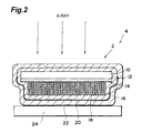
- Fig. 2 is a sectional view of a radiation image sensor 4 in accordance with an embodiment.
- one surface of a substrate 10 made of Al in the scintillator panel 2 is formed with a flat resin film 12 constituted by a polyimide resin, whereas a reflecting film 14 made of Al is formed on the surface of flat resin film 12.
- the surface of reflecting film 14 is formed with a scintillator 16, having a columnar structure, for converting incident radiation into visible light.
- Used in the scintillator 16 is CsI doped with T1.
- the scintillator 16 formed on the reflecting film 14, together with the substrate 10, is covered with a first polyparaxylylene film (first transparent organic film) 18, whereas the surface of first polyparaxylylene film 18 on the scintillator 16 side is formed with an SiO 2 film (transparent inorganic film) 20. Further, the surface of SiO 2 film 20 and the surface of the part of first polyparaxylylene film 18 not formed with the SiO 2 film 20 on the substrate 10 side are formed with a second polyparaxylylene film (second transparent organic film) 22, whereby all surfaces are covered with the second polyparaxylylene film 22. As shown in Fig. 2, the radiation image sensor 4 has a structure in which an imaging device 24 is bonded to the scintillator panel 2 on the scintillator 16 side.
- a polyimide resin is applied by a predetermined thickness (10 ⁇ m) to one surface of a rectangular substrate 10 (having a thickness of 0.5 mm) made of Al, so as to form a flat resin film 12 (see Fig. 3A). Namely, the flat resin film 12 for flattening the rolling streaks formed upon rolling the Al sheet is formed.
- an Al film 14 which is a reflecting film, is formed with a thickness of 100 nm on the surface of flat resin film 12 by vacuum vapor deposition method (see Fig. 3B).
- columnar crystals of CsI doped with Tl are grown on the surface of Al film 14 by vapor deposition method, so as to form a scintillator 16 with a thickness of 200 ⁇ m (see Fig. 3C). Since CsI forming the scintillator 16 is high in moisture absorbency so that it will deliquesce by absorbing vapor in the air if left exposed, a first polyparaxylylene film 18 is formed by CVD method in order to prevent this from occurring.
- the substrate 10 formed with the scintillator 16 is put into a CVD apparatus, so as to form the first polyparaxylylene film 18 by a thickness of 10 ⁇ m.
- the first polyparaxylylene film 18 is formed on all surfaces of the scintillator 16 and substrate 10 (see Fig. 3D). Since the tip part of scintillator 16 is uneven, the first polyparaxylylene film 18 also acts to flatten the tip part of scintillator 16.
- an SiO 2 film 20 is formed with a thickness of 200 nm by sputtering on the surface of first polyparaxylylene film 18 on the scintillator 16 side (see Fig. 4A).
- the SiO 2 film 20 is formed in an area covering the scintillator 16 since it is aimed at improving the moisture resistance of scintillator 16. Since the tip part of scintillator 16 is flattened by the first polyparaxylylene film 18 as mentioned above, the SiO 2 film 20 can be made thinner (with a thickness of 100 nm to 300 nm) so that the output light quantity would not decrease.
- a second polyparaxylylene film 22 for preventing the SiO 2 film 20 from peeling is formed with a thickness of 10 ⁇ m by CVD method on the surface of SiO 2 film 20 and the surface of first polyparaxylylene film 18 not formed with the SiO 2 film 20 on the substrate 10 side (see Fig. 4B).
- this step is completed, the making of scintillator panel 2 ends.
- the radiation image sensor 4 is made when an imaging device (CCD) 24 is bonded to thus completed scintillator panel 2 on the scintillator 16 side.
- CCD imaging device
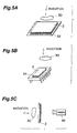
- Fig. 5A is a view showing the state where the scintillator panel 2 is coupled to a flat panel sensor (a-Si thin-film transistors with photodiodes).
- the radio-active rays transmitted through an object 30 are converted by the scintillator panel 2 into visible lights, which are then detected by the flat panel sensor.
- Fig. 5B is a view showing the state where the scintillator panel 2 is directly coupled to an imaging device (CCD) 34.
- the radio-active rays transmitted through the object 30 are converted by the scintillator panel 2 into visible lights, which is then detected by the imaging device 34.
- Fig. 5C is a view showing the state where the scintillator panel 2 is lens-coupled.
- the radio-active rays transmitted through the object 30 are converted by the scintillator panel 2 into visible lights, which are then detected by a CCD camera 36.
- the state of substrate surface would not influence characteristics of the scintillator panel 2. Also, since the reflecting film 14 is disposed on the surface of flat resin film 12, the optical output of the scintillator panel 2 can be enhanced.
- the state of substrate surface would not influence characteristics of the scintillator panel 2 involved in the radiation image sensor 4. Also, since the reflecting film 14 is disposed on the surface of flat resin film 12, the optical output of the scintillator panel 2 involved in the radiation image sensor 4 can be enhanced.
- flat resin film 12 is used as the flat resin film 12 in the above-mentioned embodiment, it is not restrictive, whereby epoxy resin, Si resin, and the like may also be used. Also, though the thickness of flat resin film 12 is set to 10 ⁇ m in the above-mentioned embodiment, any thickness can freely be chosen without being restricted to 10 ⁇ m if appropriate as long as it is such a thickness as to eliminate the unevenness in the surface of substrate 10.
- Al film is used as the reflecting film 14 in the above-mentioned embodiment, it is not restrictive; and Ag films, Au films, Pt films, and the like may also be used.
- SiO 2 film is used as the transparent inorganic film 20, it is not restrictive; and inorganic films made fromAl 2 O 3 , TiO 2 , In 2 O 3 , SnO 2 , MgO, MgF 2 , LiF, CaF 2 , AgCl, SiNO, SiN and the like may also be used.
- CsI(T1) is used as the scintillator 16 in the above-mentioned embodiment, it is not restrictive; and CsI(Na), NaI(Tl), LiI(Eu), KI(T1), and the like may also be used.
- any substrate can be used as long as it has a favorable X-ray transmissivity, whereby substrates such as those made of C (graphite) mainly composed of carbon, those made of amorphous carbon, those made of Be, those made of SiC, and the like may also be used. Substrates made of glass may be used as well.
- the SiO 2 film 20 is formed on the surface of first polyparaxylylene film 18 on the scintillator 16 side in the above-mentioned embodiment, the SiO 2 film 20 may be formed on not only the surface of first polyparaxylylene film 18 on the scintillator 16 side, but also on all surfaces of the first polyparaxylylene film 18.
- the second polyparaxylylene film 22 is formed on the surface of SiO 2 film 20 and the surface of first polyparaxylylene film 18 on the substrate 10 side, i.e., on all surfaces in the above-mentioned embodiment, the second polyparaxylylene film 22 acts to prevent the SiO 2 film 20 from peeling, whereby the material thereof is not restricted as long as the film is made of a transparent material, and it may also be formed in an area covering the SiO 2 film 20.
- polyparaxylylene film in the above-mentioned embodiment not only polyparaxylylene but also polymonochloroparaxylylene, polydichloroparaxylylene, polytetrachloroparaxylylene, polyfluoroparaxylylene, polydimethylparaxylylene, polydiethylparaxylylene, and the like can be used.
- the scintillator panel of the present invention since the scintillator is provided on the flat resin film formed on the substrate, characteristics of the scintillator panel can be kept from changing due to the state of substrate surface. Also, the scintillator plate can enhance its optical output since it has a reflecting film. In the case where the scintillator is covered with an organic film, the scintillator can be protected against vapor (moisture).
- the scintillator since the scintillator is provided on the flat resin film formed on the substrate, characteristics of the scintillator panel constituting the radiation image sensor can be kept from changing due to the state of substrate surface. Also, the scintillator plate involved in the radiation image sensor can enhance its optical output since the reflecting film is provided. When the scintillator is covered with an organic film, the scintillator constituting the radiation image sensor can be protected against vapor (moisture).
- the flat resin film is formed on the substrate, and the scintillator is formed on the flat resin film, whereby a scintillator panel whose characteristics would not change due to the state of substrate surface can be made. Also, since the reflecting film is formed on the flat resin film, the optical output of scintillator plate can be enhanced.
- the scintillator is covered with an organic film, it is possible to make a scintillator panel which can protect the scintillator against vapor (moisture).
- the flat resin film is formed on the substrate, and the scintillator is formed on the flat resin film, whereby a radiation image sensor comprising a scintillator panel whose characteristics would not change due to the state of substrate surface can be made.
- the reflecting film is formed on the flat resin film, it is possible to make a radiation image sensor which can enhance the optical output of scintillator plate.
- the scintillator is covered with an organic film, it is possible to make a radiation image sensor comprising a scintillator panel which can protect the scintillator against vapor (moisture).
- the scintillator panel and radiation image sensor in accordance with the present invention are suitably usable for medical and industrial X-ray photography and the like.
Landscapes
- Physics & Mathematics (AREA)
- General Physics & Mathematics (AREA)
- High Energy & Nuclear Physics (AREA)
- Health & Medical Sciences (AREA)
- Life Sciences & Earth Sciences (AREA)
- Molecular Biology (AREA)
- Spectroscopy & Molecular Physics (AREA)
- Chemical & Material Sciences (AREA)
- Crystallography & Structural Chemistry (AREA)
- Engineering & Computer Science (AREA)
- General Engineering & Computer Science (AREA)
- Measurement Of Radiation (AREA)
- Conversion Of X-Rays Into Visible Images (AREA)
Applications Claiming Priority (3)
| Application Number | Priority Date | Filing Date | Title |
|---|---|---|---|
| JP17119198 | 1998-06-18 | ||
| JP17119198 | 1998-06-18 | ||
| PCT/JP1999/003264 WO1999066348A1 (en) | 1998-06-18 | 1999-06-18 | Scintillator panel, radiation image sensor, and method for producing the same |
Publications (3)
| Publication Number | Publication Date |
|---|---|
| EP1118878A1 true EP1118878A1 (de) | 2001-07-25 |
| EP1118878A4 EP1118878A4 (de) | 2001-09-26 |
| EP1118878B1 EP1118878B1 (de) | 2005-08-17 |
Family
ID=15918706
Family Applications (1)
| Application Number | Title | Priority Date | Filing Date |
|---|---|---|---|
| EP99925377A Expired - Lifetime EP1118878B1 (de) | 1998-06-18 | 1999-06-18 | Szintillatorpanel, strahlungsbildsensor und verfahren zu deren herstellung |
Country Status (8)
| Country | Link |
|---|---|
| US (2) | US6469307B2 (de) |
| EP (1) | EP1118878B1 (de) |
| JP (1) | JP4279462B2 (de) |
| KR (1) | KR100389980B1 (de) |
| CN (1) | CN1152265C (de) |
| AU (1) | AU4168199A (de) |
| DE (1) | DE69926769T2 (de) |
| WO (1) | WO1999066348A1 (de) |
Cited By (11)
| Publication number | Priority date | Publication date | Assignee | Title |
|---|---|---|---|---|
| US6753531B2 (en) | 1999-04-09 | 2004-06-22 | Hamamatsu Photonics K.K. | Scintillator panel and radiation image sensor |
| EP1286363A3 (de) * | 2001-08-23 | 2005-10-05 | Agfa-Gevaert N.V. | Leuchtstoffträger mit guter Feuchtigkeitsbeständigkeit |
| US7034306B2 (en) | 1998-06-18 | 2006-04-25 | Hamamatsu Photonics K.K. | Scintillator panel and radiation image sensor |
| EP1231483A3 (de) * | 2001-02-07 | 2006-08-30 | Canon Kabushiki Kaisha | Szintillator-Panel, Strahlungsdetektorvorrichtung und Verfahren zu deren Herstellung |
| EP1435627A3 (de) * | 2002-12-26 | 2007-05-30 | Konica Minolta Holdings, Inc. | Strahlungsbildwandler |
| EP1376615A3 (de) * | 2002-06-28 | 2007-08-08 | Agfa HealthCare NV | Bindemittelfreier Aufzeichnungs-Leuchtbildschirm |
| EP1376616A3 (de) * | 2002-06-28 | 2007-08-08 | Agfa HealthCare NV | Bindemittelfreier Aufzeichnungs-Leuchtbildschirm mit einem Träger der eine amorphe Kohlenstoffschicht beinhaltet |
| EP1437744A3 (de) * | 2003-01-09 | 2007-08-15 | Konica Minolta Holdings, Inc. | Strahlungsbildwandler |
| WO2007134914A1 (de) * | 2006-05-24 | 2007-11-29 | Siemens Aktiengesellschaft | Szintillatorplatte |
| US7718974B2 (en) | 2006-08-21 | 2010-05-18 | Siemens Aktiengesellschaft | X-ray converter element |
| GB2477346A (en) * | 2010-02-01 | 2011-08-03 | Applied Scintillation Technologies Ltd | Scintillator assembly for use in digital x-ray imaging |
Families Citing this family (34)
| Publication number | Priority date | Publication date | Assignee | Title |
|---|---|---|---|---|
| DE69913185T2 (de) * | 1998-06-18 | 2004-08-26 | Hamamatsu Photonics K.K., Hamamatsu | Verfahren zur abscheidung eines organischen films |
| EP1258738B1 (de) * | 2000-01-13 | 2011-08-03 | Hamamatsu Photonics K.K. | Strahlungsbildsensor und szintillatortafel |
| WO2002023220A1 (en) * | 2000-09-11 | 2002-03-21 | Hamamatsu Photonics K.K. | Scintillator panel, radiation image sensor and methods of producing them |
| WO2002023219A1 (en) | 2000-09-11 | 2002-03-21 | Hamamatsu Photonics K.K. | Scintillator panel, radiation image sensor and methods of producing them |
| KR20030072606A (ko) * | 2001-01-30 | 2003-09-15 | 하마마츠 포토닉스 가부시키가이샤 | 신틸레이터 패널 및 방사선 이미지 센서 |
| JP4878427B2 (ja) * | 2001-09-07 | 2012-02-15 | キヤノン株式会社 | シンチレータパネル、放射線撮像装置及び放射線検出システム |
| US6847041B2 (en) * | 2001-02-09 | 2005-01-25 | Canon Kabushiki Kaisha | Scintillator panel, radiation detector and manufacture methods thereof |
| JP4587432B2 (ja) * | 2001-08-30 | 2010-11-24 | キヤノン株式会社 | シンチレータパネル、放射線検出装置及びシステム |
| JP4323827B2 (ja) * | 2003-02-14 | 2009-09-02 | キヤノン株式会社 | 固体撮像装置及び放射線撮像装置 |
| US7355184B2 (en) * | 2003-04-07 | 2008-04-08 | Canon Kabushiki Kaisha | Radiation detecting apparatus and method for manufacturing the same |
| WO2005038490A1 (en) * | 2003-10-22 | 2005-04-28 | Canon Kabushiki Kaisha | Radiation detection device, scintillator panel, method of making the same, making apparatus, and radiation image pick-up system |
| EP1681584B1 (de) * | 2005-01-13 | 2009-09-09 | Aloka Co., Ltd. | Szintillatorteil und Herstellungsverfahren dafür sowie Strahlungsmessvorrichtung |
| US7772558B1 (en) * | 2006-03-29 | 2010-08-10 | Radiation Monitoring Devices, Inc. | Multi-layer radiation detector and related methods |
| DE102006022138A1 (de) * | 2006-05-11 | 2007-11-15 | Siemens Ag | Szintillatorplatte |
| US7732788B2 (en) * | 2007-10-23 | 2010-06-08 | Hamamatsu Photonics K.K. | Radiation image converting panel, scintillator panel and radiation image sensor |
| US7465932B1 (en) | 2007-06-15 | 2008-12-16 | Hamamatsu Photonics K.K. | Radiation image conversion panel, scintillator panel, and radiation image sensor |
| US7468514B1 (en) * | 2007-06-15 | 2008-12-23 | Hamamatsu Photonics K.K. | Radiation image conversion panel, scintillator panel, and radiation image sensor |
| US7977646B2 (en) * | 2008-04-17 | 2011-07-12 | Saint-Gobain Ceramics & Plastics, Inc. | Scintillation detector reflector |
| JP5353886B2 (ja) * | 2008-07-18 | 2013-11-27 | コニカミノルタ株式会社 | 放射線シンチレータおよび放射線画像検出器 |
| JP5402933B2 (ja) * | 2008-08-28 | 2014-01-29 | コニカミノルタ株式会社 | 放射線画像変換パネル及びその製造方法 |
| CN101604118B (zh) * | 2008-12-31 | 2012-07-04 | 中国工程物理研究院流体物理研究所 | 一种将高能x射线图像转换为可见光图像的装置 |
| CN101738631B (zh) * | 2009-12-29 | 2012-10-10 | 上海新漫传感技术研究发展有限公司 | 一种碘化锂闪烁探测器及其制备方法 |
| CN101900824B (zh) * | 2010-06-24 | 2012-05-09 | 江苏康众数字医疗设备有限公司 | 闪烁体封装薄膜及封装方法 |
| JP5728250B2 (ja) * | 2011-03-01 | 2015-06-03 | キヤノン株式会社 | 放射線検出装置、シンチレータパネル、それらの製造方法、および放射線検出システム |
| JP5922518B2 (ja) * | 2012-07-20 | 2016-05-24 | 浜松ホトニクス株式会社 | シンチレータパネル及び放射線検出器 |
| JP6298264B2 (ja) | 2012-10-31 | 2018-03-20 | キヤノン株式会社 | シンチレータ、放射線検出装置、および、それらの製造方法 |
| CN104022047B (zh) * | 2014-06-10 | 2018-02-16 | 平生医疗科技(昆山)有限公司 | 一种易潮解性辐射晶体面板的封装方法及结构 |
| WO2016153335A1 (en) * | 2015-03-20 | 2016-09-29 | Perkinelmer Health Sciences B.V. | Scintillator |
| JP6487263B2 (ja) * | 2015-04-20 | 2019-03-20 | 浜松ホトニクス株式会社 | 放射線検出器及びその製造方法 |
| JP6433560B1 (ja) | 2017-09-27 | 2018-12-05 | 浜松ホトニクス株式会社 | シンチレータパネル及び放射線検出器 |
| US20180061608A1 (en) * | 2017-09-28 | 2018-03-01 | Oxford Instruments X-ray Technology Inc. | Window member for an x-ray device |
| JP7325295B2 (ja) * | 2019-10-24 | 2023-08-14 | 浜松ホトニクス株式会社 | シンチレータパネル、放射線検出器、シンチレータパネルの製造方法、及び、放射線検出器の製造方法 |
| CN113933324B (zh) | 2020-06-29 | 2023-07-14 | 京东方科技集团股份有限公司 | 平板探测器及其制造方法 |
| CN114966804A (zh) * | 2022-04-25 | 2022-08-30 | 中国科学院微电子研究所 | 极紫外光用的闪烁体组件及应用、间接探测器系统 |
Family Cites Families (16)
| Publication number | Priority date | Publication date | Assignee | Title |
|---|---|---|---|---|
| US4543485A (en) * | 1981-11-24 | 1985-09-24 | Hitachi Chemical Company, Ltd. | Scintillator for radiation detection and process for producing the same |
| JPH077114B2 (ja) | 1987-03-04 | 1995-01-30 | コニカ株式会社 | 加熱乾燥手段を有するx線写真増感用蛍光体パネル |
| JPS63215987A (ja) * | 1987-03-04 | 1988-09-08 | Hamamatsu Photonics Kk | 高解像シンチレ−シヨンフアイバ−プレ−ト |
| JP2611295B2 (ja) * | 1987-12-28 | 1997-05-21 | 株式会社日立製作所 | 放射線検出器およびその製造方法 |
| JPH0697280B2 (ja) | 1988-02-05 | 1994-11-30 | 富士写真フイルム株式会社 | 放射線像変換パネル |
| US5168540A (en) * | 1990-09-12 | 1992-12-01 | Advanced Technology Materials Inc. | Scintillating articles and method of making the same |
| US5153438A (en) | 1990-10-01 | 1992-10-06 | General Electric Company | Method of forming an x-ray imaging array and the array |
| JP3034587B2 (ja) * | 1990-11-07 | 2000-04-17 | コニカ株式会社 | 放射線画像変換パネル |
| US5179284A (en) | 1991-08-21 | 1993-01-12 | General Electric Company | Solid state radiation imager having a reflective and protective coating |
| US5132539A (en) | 1991-08-29 | 1992-07-21 | General Electric Company | Planar X-ray imager having a moisture-resistant sealing structure |
| US5148029A (en) * | 1991-09-23 | 1992-09-15 | Siemens Gammasonics, Inc. | Improved seal scintillation camera module and method of making it |
| JPH0721560A (ja) | 1993-06-30 | 1995-01-24 | Sony Corp | 磁気記録媒体の製造方法 |
| JPH07218698A (ja) | 1994-01-28 | 1995-08-18 | Sony Corp | 蛍光板およびそれを利用した放射線撮影装置、並びに蛍光板の製造方法 |
| JP3075134B2 (ja) | 1995-04-04 | 2000-08-07 | 株式会社日立製作所 | 反射型液晶表示装置 |
| FR2774175B1 (fr) | 1998-01-27 | 2000-04-07 | Thomson Csf | Capteur electronique matriciel photosensible |
| US6835936B2 (en) | 2001-02-07 | 2004-12-28 | Canon Kabushiki Kaisha | Scintillator panel, method of manufacturing scintillator panel, radiation detection device, and radiation detection system |
-
1999
- 1999-06-18 KR KR10-2000-7014388A patent/KR100389980B1/ko not_active Expired - Lifetime
- 1999-06-18 DE DE69926769T patent/DE69926769T2/de not_active Expired - Lifetime
- 1999-06-18 AU AU41681/99A patent/AU4168199A/en not_active Abandoned
- 1999-06-18 CN CNB998074039A patent/CN1152265C/zh not_active Expired - Lifetime
- 1999-06-18 WO PCT/JP1999/003264 patent/WO1999066348A1/ja not_active Ceased
- 1999-06-18 JP JP2000555113A patent/JP4279462B2/ja not_active Expired - Fee Related
- 1999-06-18 EP EP99925377A patent/EP1118878B1/de not_active Expired - Lifetime
-
2000
- 2000-12-18 US US09/737,819 patent/US6469307B2/en not_active Ceased
-
2003
- 2003-10-21 US US10/689,578 patent/USRE39806E1/en not_active Expired - Lifetime
Cited By (17)
| Publication number | Priority date | Publication date | Assignee | Title |
|---|---|---|---|---|
| US7705315B2 (en) | 1998-06-18 | 2010-04-27 | Hamamatsu Photonics K.K. | Scintillator panel and radiation image sensor |
| US7034306B2 (en) | 1998-06-18 | 2006-04-25 | Hamamatsu Photonics K.K. | Scintillator panel and radiation image sensor |
| US7408177B2 (en) | 1998-06-18 | 2008-08-05 | Hamamatsu Photonics K.K. | Scintillator panel and radiation image sensor |
| US6911658B2 (en) | 1999-04-09 | 2005-06-28 | Hamamatsu Photonics K.K. | Scintillator panel and radiation image sensor |
| US6753531B2 (en) | 1999-04-09 | 2004-06-22 | Hamamatsu Photonics K.K. | Scintillator panel and radiation image sensor |
| EP1231483A3 (de) * | 2001-02-07 | 2006-08-30 | Canon Kabushiki Kaisha | Szintillator-Panel, Strahlungsdetektorvorrichtung und Verfahren zu deren Herstellung |
| EP2357495A1 (de) * | 2001-02-07 | 2011-08-17 | Canon Kabushiki Kaisha | Szintillator-Panel |
| EP1286363A3 (de) * | 2001-08-23 | 2005-10-05 | Agfa-Gevaert N.V. | Leuchtstoffträger mit guter Feuchtigkeitsbeständigkeit |
| EP1376615A3 (de) * | 2002-06-28 | 2007-08-08 | Agfa HealthCare NV | Bindemittelfreier Aufzeichnungs-Leuchtbildschirm |
| EP1376616A3 (de) * | 2002-06-28 | 2007-08-08 | Agfa HealthCare NV | Bindemittelfreier Aufzeichnungs-Leuchtbildschirm mit einem Träger der eine amorphe Kohlenstoffschicht beinhaltet |
| EP1435627A3 (de) * | 2002-12-26 | 2007-05-30 | Konica Minolta Holdings, Inc. | Strahlungsbildwandler |
| EP1437744A3 (de) * | 2003-01-09 | 2007-08-15 | Konica Minolta Holdings, Inc. | Strahlungsbildwandler |
| WO2007134914A1 (de) * | 2006-05-24 | 2007-11-29 | Siemens Aktiengesellschaft | Szintillatorplatte |
| US7718974B2 (en) | 2006-08-21 | 2010-05-18 | Siemens Aktiengesellschaft | X-ray converter element |
| DE102006038969B4 (de) * | 2006-08-21 | 2013-02-28 | Siemens Aktiengesellschaft | Röntgenkonverterelement und Verfahren zu dessen Herstellung |
| GB2477346A (en) * | 2010-02-01 | 2011-08-03 | Applied Scintillation Technologies Ltd | Scintillator assembly for use in digital x-ray imaging |
| GB2477346B (en) * | 2010-02-01 | 2016-03-23 | Scintacor Ltd | Scintillator assembly for use in digital x-ray imaging |
Also Published As
| Publication number | Publication date |
|---|---|
| JP4279462B2 (ja) | 2009-06-17 |
| DE69926769T2 (de) | 2006-06-29 |
| DE69926769D1 (de) | 2005-09-22 |
| USRE39806E1 (en) | 2007-09-04 |
| CN1152265C (zh) | 2004-06-02 |
| US6469307B2 (en) | 2002-10-22 |
| AU4168199A (en) | 2000-01-05 |
| KR20010071511A (ko) | 2001-07-28 |
| EP1118878A4 (de) | 2001-09-26 |
| KR100389980B1 (ko) | 2003-07-12 |
| EP1118878B1 (de) | 2005-08-17 |
| CN1305595A (zh) | 2001-07-25 |
| US20020074502A1 (en) | 2002-06-20 |
| WO1999066348A1 (en) | 1999-12-23 |
Similar Documents
| Publication | Publication Date | Title |
|---|---|---|
| EP1118878B1 (de) | Szintillatorpanel, strahlungsbildsensor und verfahren zu deren herstellung | |
| JP3789785B2 (ja) | 放射線イメージセンサ | |
| EP1211521B1 (de) | Szintillatorpanel und strahlungsbildsensor | |
| EP1115011A1 (de) | Strahlungsbildsensor | |
| US7034306B2 (en) | Scintillator panel and radiation image sensor | |
| EP1118879A1 (de) | Szintillatorpanel und strahlungsbildsensor | |
| EP1139120B1 (de) | Strahlungsbildsensor und verfahren zu dessen herstellung | |
| JPWO1999066348A1 (ja) | シンチレータパネル、放射線イメージセンサ及びその製造方法 | |
| US6753531B2 (en) | Scintillator panel and radiation image sensor | |
| JPH0593780A (ja) | 放射線検出素子 | |
| JP4083874B2 (ja) | シンチレータファイバプレート及び放射線イメージセンサ | |
| EP1862821A1 (de) | Szintillatorvorrichtung und Strahlungsbildsensor | |
| JPWO1999066346A1 (ja) | シンチレータプレート放射線イメージセンサ及びその製造方法 |
Legal Events
| Date | Code | Title | Description |
|---|---|---|---|
| PUAI | Public reference made under article 153(3) epc to a published international application that has entered the european phase |
Free format text: ORIGINAL CODE: 0009012 |
|
| 17P | Request for examination filed |
Effective date: 20010115 |
|
| AK | Designated contracting states |
Kind code of ref document: A1 Designated state(s): DE FR GB IT NL SE |
|
| A4 | Supplementary search report drawn up and despatched |
Effective date: 20010816 |
|
| AK | Designated contracting states |
Kind code of ref document: A4 Designated state(s): DE FR GB IT NL SE |
|
| RIC1 | Information provided on ipc code assigned before grant |
Free format text: 7G 01T 1/20 A, 7G 01T 1/24 B, 7G 21K 4/00 B |
|
| 17Q | First examination report despatched |
Effective date: 20040323 |
|
| GRAP | Despatch of communication of intention to grant a patent |
Free format text: ORIGINAL CODE: EPIDOSNIGR1 |
|
| GRAS | Grant fee paid |
Free format text: ORIGINAL CODE: EPIDOSNIGR3 |
|
| GRAA | (expected) grant |
Free format text: ORIGINAL CODE: 0009210 |
|
| AK | Designated contracting states |
Kind code of ref document: B1 Designated state(s): DE FR GB IT NL SE |
|
| REG | Reference to a national code |
Ref country code: GB Ref legal event code: FG4D |
|
| REF | Corresponds to: |
Ref document number: 69926769 Country of ref document: DE Date of ref document: 20050922 Kind code of ref document: P |
|
| REG | Reference to a national code |
Ref country code: SE Ref legal event code: TRGR |
|
| ET | Fr: translation filed | ||
| PLBE | No opposition filed within time limit |
Free format text: ORIGINAL CODE: 0009261 |
|
| STAA | Information on the status of an ep patent application or granted ep patent |
Free format text: STATUS: NO OPPOSITION FILED WITHIN TIME LIMIT |
|
| 26N | No opposition filed |
Effective date: 20060518 |
|
| REG | Reference to a national code |
Ref country code: FR Ref legal event code: PLFP Year of fee payment: 18 |
|
| REG | Reference to a national code |
Ref country code: FR Ref legal event code: PLFP Year of fee payment: 19 |
|
| REG | Reference to a national code |
Ref country code: FR Ref legal event code: PLFP Year of fee payment: 20 |
|
| PGFP | Annual fee paid to national office [announced via postgrant information from national office to epo] |
Ref country code: DE Payment date: 20180605 Year of fee payment: 20 |
|
| PGFP | Annual fee paid to national office [announced via postgrant information from national office to epo] |
Ref country code: NL Payment date: 20180514 Year of fee payment: 20 Ref country code: FR Payment date: 20180511 Year of fee payment: 20 |
|
| PGFP | Annual fee paid to national office [announced via postgrant information from national office to epo] |
Ref country code: SE Payment date: 20180612 Year of fee payment: 20 |
|
| PGFP | Annual fee paid to national office [announced via postgrant information from national office to epo] |
Ref country code: IT Payment date: 20180625 Year of fee payment: 20 Ref country code: GB Payment date: 20180613 Year of fee payment: 20 |
|
| REG | Reference to a national code |
Ref country code: DE Ref legal event code: R071 Ref document number: 69926769 Country of ref document: DE |
|
| REG | Reference to a national code |
Ref country code: NL Ref legal event code: MK Effective date: 20190617 |
|
| REG | Reference to a national code |
Ref country code: GB Ref legal event code: PE20 Expiry date: 20190617 |
|
| REG | Reference to a national code |
Ref country code: SE Ref legal event code: EUG |
|
| PG25 | Lapsed in a contracting state [announced via postgrant information from national office to epo] |
Ref country code: GB Free format text: LAPSE BECAUSE OF EXPIRATION OF PROTECTION Effective date: 20190617 |