EP1097980B1 - Bathophenanthroline compound and process for preparing same - Google Patents
Bathophenanthroline compound and process for preparing same Download PDFInfo
- Publication number
- EP1097980B1 EP1097980B1 EP00123668A EP00123668A EP1097980B1 EP 1097980 B1 EP1097980 B1 EP 1097980B1 EP 00123668 A EP00123668 A EP 00123668A EP 00123668 A EP00123668 A EP 00123668A EP 1097980 B1 EP1097980 B1 EP 1097980B1
- Authority
- EP
- European Patent Office
- Prior art keywords
- group
- organic
- layer
- bathophenanthroline
- hexane
- Prior art date
- Legal status (The legal status is an assumption and is not a legal conclusion. Google has not performed a legal analysis and makes no representation as to the accuracy of the status listed.)
- Expired - Lifetime
Links
- 0 Cc(c(-c1ccccc1)c1*)cc(C)c1-c(cc(-c1ccccc1)c1ccc2c(-c3ccccc3)c3)nc1c2nc3-c(c(C)c(c(C)c1)-c2ccccc2)c1N Chemical compound Cc(c(-c1ccccc1)c1*)cc(C)c1-c(cc(-c1ccccc1)c1ccc2c(-c3ccccc3)c3)nc1c2nc3-c(c(C)c(c(C)c1)-c2ccccc2)c1N 0.000 description 4
- PAFZNILMFXTMIY-UHFFFAOYSA-N NC1CCCCC1 Chemical compound NC1CCCCC1 PAFZNILMFXTMIY-UHFFFAOYSA-N 0.000 description 1
Images


Classifications
-
- C—CHEMISTRY; METALLURGY
- C07—ORGANIC CHEMISTRY
- C07D—HETEROCYCLIC COMPOUNDS
- C07D471/00—Heterocyclic compounds containing nitrogen atoms as the only ring hetero atoms in the condensed system, at least one ring being a six-membered ring with one nitrogen atom, not provided for by groups C07D451/00 - C07D463/00
- C07D471/02—Heterocyclic compounds containing nitrogen atoms as the only ring hetero atoms in the condensed system, at least one ring being a six-membered ring with one nitrogen atom, not provided for by groups C07D451/00 - C07D463/00 in which the condensed system contains two hetero rings
- C07D471/04—Ortho-condensed systems
-
- H—ELECTRICITY
- H10—SEMICONDUCTOR DEVICES; ELECTRIC SOLID-STATE DEVICES NOT OTHERWISE PROVIDED FOR
- H10K—ORGANIC ELECTRIC SOLID-STATE DEVICES
- H10K85/00—Organic materials used in the body or electrodes of devices covered by this subclass
- H10K85/60—Organic compounds having low molecular weight
- H10K85/649—Aromatic compounds comprising a hetero atom
- H10K85/657—Polycyclic condensed heteroaromatic hydrocarbons
- H10K85/6572—Polycyclic condensed heteroaromatic hydrocarbons comprising only nitrogen in the heteroaromatic polycondensed ring system, e.g. phenanthroline or carbazole
-
- H—ELECTRICITY
- H10—SEMICONDUCTOR DEVICES; ELECTRIC SOLID-STATE DEVICES NOT OTHERWISE PROVIDED FOR
- H10K—ORGANIC ELECTRIC SOLID-STATE DEVICES
- H10K2102/00—Constructional details relating to the organic devices covered by this subclass
- H10K2102/10—Transparent electrodes, e.g. using graphene
- H10K2102/101—Transparent electrodes, e.g. using graphene comprising transparent conductive oxides [TCO]
- H10K2102/103—Transparent electrodes, e.g. using graphene comprising transparent conductive oxides [TCO] comprising indium oxides, e.g. ITO
-
- H—ELECTRICITY
- H10—SEMICONDUCTOR DEVICES; ELECTRIC SOLID-STATE DEVICES NOT OTHERWISE PROVIDED FOR
- H10K—ORGANIC ELECTRIC SOLID-STATE DEVICES
- H10K50/00—Organic light-emitting devices
- H10K50/10—OLEDs or polymer light-emitting diodes [PLED]
- H10K50/11—OLEDs or polymer light-emitting diodes [PLED] characterised by the electroluminescent [EL] layers
-
- H—ELECTRICITY
- H10—SEMICONDUCTOR DEVICES; ELECTRIC SOLID-STATE DEVICES NOT OTHERWISE PROVIDED FOR
- H10K—ORGANIC ELECTRIC SOLID-STATE DEVICES
- H10K85/00—Organic materials used in the body or electrodes of devices covered by this subclass
- H10K85/30—Coordination compounds
- H10K85/321—Metal complexes comprising a group IIIA element, e.g. Tris (8-hydroxyquinoline) gallium [Gaq3]
- H10K85/324—Metal complexes comprising a group IIIA element, e.g. Tris (8-hydroxyquinoline) gallium [Gaq3] comprising aluminium, e.g. Alq3
-
- H—ELECTRICITY
- H10—SEMICONDUCTOR DEVICES; ELECTRIC SOLID-STATE DEVICES NOT OTHERWISE PROVIDED FOR
- H10K—ORGANIC ELECTRIC SOLID-STATE DEVICES
- H10K85/00—Organic materials used in the body or electrodes of devices covered by this subclass
- H10K85/60—Organic compounds having low molecular weight
- H10K85/615—Polycyclic condensed aromatic hydrocarbons, e.g. anthracene
- H10K85/626—Polycyclic condensed aromatic hydrocarbons, e.g. anthracene containing more than one polycyclic condensed aromatic rings, e.g. bis-anthracene
-
- Y—GENERAL TAGGING OF NEW TECHNOLOGICAL DEVELOPMENTS; GENERAL TAGGING OF CROSS-SECTIONAL TECHNOLOGIES SPANNING OVER SEVERAL SECTIONS OF THE IPC; TECHNICAL SUBJECTS COVERED BY FORMER USPC CROSS-REFERENCE ART COLLECTIONS [XRACs] AND DIGESTS
- Y10—TECHNICAL SUBJECTS COVERED BY FORMER USPC
- Y10S—TECHNICAL SUBJECTS COVERED BY FORMER USPC CROSS-REFERENCE ART COLLECTIONS [XRACs] AND DIGESTS
- Y10S428/00—Stock material or miscellaneous articles
- Y10S428/917—Electroluminescent
Definitions
- This invention relates to a bathophenanthroline compound, which is adapted for use in an organic electroluminescent device (e.g. an organic electroluminescent device suitable as a display device or a light-emitting device such as a spontaneous light flat display, especially an organic electroluminescent color display using an organic thin film as an electroluminescent layer), and also a process for preparing the compound.
- an organic electroluminescent device e.g. an organic electroluminescent device suitable as a display device or a light-emitting device such as a spontaneous light flat display, especially an organic electroluminescent color display using an organic thin film as an electroluminescent layer
- an organic electroluminescent device e.g. an organic electroluminescent device suitable as a display device or a light-emitting device such as a spontaneous light flat display, especially an organic electroluminescent color display using an organic thin film as an electroluminescent layer
- liquid crystal displays are employed as an interface of a diversity of articles and have wide utility in the fields not only of lap top-type information processors, but also of articles for our daily use including small-sized television sets, watches, desk-top calculators and the like.
- liquid crystal displays have been studied as a key of display devices, which are used as the interface connecting a human being and a machine and cover small-sized to large capacitance display devices while making use of the feature that liquid crystals are low in drive voltage and power consumption.
- liquid crystal displays have the problems that they do not rely on spontaneous light and thus need a greater power consumption for back light drive than for liquid crystal drive, with the result that a service time is shortened when using a built-in battery, thus placing a limitation on their use.
- the liquid crystal display has another problem that it has such a narrow angle of field as not to be suitable for use as a large-sized display device.
- liquid crystal display depends on the manner of display using the orientation of liquid crystal molecules, and this is considered to bring about a serious problem that its contrast changes depending on the angle even within an angle of field.
- an active matrix system which is one of drive systems, has a response speed sufficient to deal with a motion picture.
- a TFT (thin film transistor) drive circuit is used, a difficulty is involved in making a large screen size owing to the pixel defects, thus being disadvantageous in view of the reduction in cost.
- a simple matrix system which is another type of drive system, is not only low in cost, but also relatively easy in making a large screen size.
- this system has the problem that its response speed is not enough to deal with a motion picture.
- a spontaneous light display device is now under study such as on a plasma display device, an inorganic electroluminescent device, an organic electroluminescent device and the like.
- the plasma display device employs plasma emission in a low pressure gas for display and is suited for the purposes of a large size and large capacitance, but has the problem on thinning and costs.
- an AC bias of high potential is required for its drive, and thus, the display is not suitable as a portable device.
- the inorganic electroluminescent device has been put on the market as a green light emission display. Like the plasma display device, an AC bias drive is essential, for which several hundreds of volts are necessary, thus not being of practical use.
- the electroluminescent phenomenon caused by organic compounds has been long studied ever since there was discovered a luminescent or emission phenomenon wherein carriers are injected into the single crystal of anthracene capable of emitting a strong fluorescence in the first part of 1960s.
- fluorescence is low in brightness and monochronous in nature, and the single crystal is used, so that this emission has been made as a fundamental investigation of carrier injection into organic materials.
- the organic electroluminescent device (which may be sometimes referred to as organic EL device hereinafter) has a film thickness of 1 ⁇ m or below.
- organic EL device When an electric current is charged to the device, the electric energy is converted to a light energy thereby causing luminescence to be emitted in the form of a plane.
- the device has an ideal feature for use as a display device of the spontaneous emission type.
- Fig. 7 shows an example of a known organic EL device.
- An organic EL device 10 includes, on a transparent substrate 6 (e.g. a glass substrate), an ITO (indium tin oxide) transparent electrode 5, a hole transport layer 4, an emission layer 3, an electron transport layer 2, and a cathode 1 (e.g. an aluminium electrode) formed in this order, for example, by a vacuum deposition method.
- a transparent substrate 6 e.g. a glass substrate
- ITO indium tin oxide
- hole transport layer 4 an emission layer 3
- electron transport layer 2 an electron transport layer 2
- a cathode 1 e.g. an aluminium electrode
- a DC voltage 7 is selectively applied between the transparent electrode 5 serving as an anode and the cathode 1, so that holes serving as carriers charged from the transparent electrode 5 are moved via the hole transport layer 4, and electrons charged from the cathode 1 are moved via the electron transport layer 2, thereby causing the re-combination of the electrons-holes. From the site of the re-combination, light 8 with a given wavelength is emitted and can be observed from the side of the transparent substrate 6.
- the emission layer 3 may be made of a light-emitting substance such as, for example, anthracene, naphthalene, phenanthrene, pyrene, chrysene, perylene, butadiene, coumarin, acridine, stilbene and the like. This may be contained in the electron transport layer 2.
- a light-emitting substance such as, for example, anthracene, naphthalene, phenanthrene, pyrene, chrysene, perylene, butadiene, coumarin, acridine, stilbene and the like. This may be contained in the electron transport layer 2.
- Fig. 8 shows another example of an organic EL device.
- the emission layer 3 as in Fig. 7 is omitted and, instead, such a light-emitting substance as mentioned above is contained in the electron transport layer 2, and thus, the organic EL device 20 is so arranged as to emit light 18 having a given wavelength from an interface between the electron transport layer 2 and the hole transport layer 4.
- Fig. 9 shows an application of the organic EL device. More particularly, a built-up body of the respective organic layers (including the hole transport layer 4, and the emission layer 3 or the electron transport layer 2) is interposed between the cathode 1 and the anode 5. These electrodes are, respectively, provided in the form of stripes that are intersected in the form of a matrix. In this state, a signal voltage is applied to in time series by means of a luminance signal circuit 34 and a shift register-built in control circuit 35 so that light is emitted at a number of intersected points (pixels), respectively.
- a luminance signal circuit 34 and a shift register-built in control circuit 35 so that light is emitted at a number of intersected points (pixels), respectively.
- Such an arrangement as set out above is usable not only as a display, but also as an image reproducing apparatus. It will be noted that if the striped pattern is provided for the respective colors of R, G and B, there can be obtained a full color or a multi-color arrangement.
- emitting organic thin film layers 2, 3 and 4 are usually sandwiched between the transparent electrode 5 and the metal electrode 1, and emission occurs at the side of the transparent electrode 5.
- organic luminescent materials and carrier transport materials suitable for use in combination with the organic luminescent materials For use as constituting materials of the organic EL device, attention has now been drawn to organic luminescent materials and carrier transport materials suitable for use in combination with the organic luminescent materials.
- the advantages of these organic materials reside in that their optical and electrical properties can be controlled to some extent through the molecular design thereof.
- an organic luminescent material having a given light emission and a carrier transport material suited therewith are used in combination, efficient light emission is ensured. Accordingly, there can be realized a full color organic EL device wherein primaries of R, G and B are emitted using the respective luminescent materials.
- such an organic EL device as set out above may have such a structure that a hole transport layer serves also as a luminescent element.
- a hole transport layer serves also as a luminescent element.
- it is essential to provide a carrier transport layer that is able to efficiently transport electrons and block holes.
- organic materials that satisfy the above requirement and the efficient manufacture of these materials have never been found yet. Sugihara H. et al. (Analytical Science, (1993), 593 - 597 ) relates to lithium ion-selective electrodes based on 1,10-phenanthroline derivatives.
- Dietrich-Buchecker C.O. et al. discloses that the reaction of an alkyl- or aryllithium with 1,10-phenanthroline followed by hydrolysis and rearomatisation with managenese dioxide gives good yields of the 2,9-disubstitued product.
- WO 99/53724 relates to color-tunable organic light emitting devices and EP 0 564 224 A2 deals with organic electroluminescent devices.
- An object of the invention is to provide a novel organic material, which is suitable for use as a carrier transport material capable of efficiently transporting electrons and blocking holes.
- Another object of the invention is to provide a process for preparing such an organic compound as mentioned above in an efficient manner.
- the bathophenanthroline compound of the invention can control carrier transportability depending on the type of substituent introduced into the molecule, and can thus be utilizable as a carrier transport material of various types of organic EL devices.
- the compounds have high glass transition point and high melting point and are stable electrically, thermally and/or chemically.
- the compounds are sublimable in nature, which is advantageous in that a uniform amorphous film can be readily formed according to a vacuum deposition process.
- R 1 and R 2 , and Ar 1 and Ar 2 are, respectively, the same.
- aryl group used herein means a carbocyclic aromatic group such as, for example, a phenyl group, a naphthyl group, an anthryl group or the like, and a heterocyclic aromatic group such as, for example, a furyl group, a thienyl group, a pyridyl group or the like.
- a process for perparing a bathophenanthroline compound which comprising subjecting a lithium compound of the following general formula [III] or [V]
- R 3 -Li or R 4 -Li wherein R 3 and R 4 may be the same or different and independently represent a linear, branched or cyclic, saturated or unsaturated hydrocarbon group or a substituted or unsubstituted, saturated or unsaturated hydrocarbon group provided that at least one of R 3 and R 4 has at least two carbon atoms
- the bathophenanthroline compound of the invention can be efficiently prepared. It is preferred that in the course of the nucleophilic substitution reaction, carbanions are generated from the lithium compound and subsequently reacted with the bathophenanthroline.
- R 1 and R 2 independently represent a linear, branched or cyclic, saturated or unsaturated hydrocarbon group, which are an ethyl group, a butyl group, an n-propyl group, an isopropyl group, an n-butyl group, a sec-butyl group, a tert-butyl group, an n-pentyl group, an iso-pentyl group, a neopentyl group, a tert-pentyl group, a cyclopentyl group, an n-hexyl group, a 2-ethylbutyl group, a 3,3-dimethylbutyl group, a cyclohexyl group, an n-heptyl group, a cyclohexylmethyl group, an n-octyl group, a tert
- the substituted or unsubstituted, saturated and unsaturated hydrocarbon group for R 1 and R 2 is also a benzyl group, a phenethyl group, an ⁇ -methylbenzyl group, an ⁇ , ⁇ -dimethylbenzyl group, a 1-naphthylmethyl group, a 2-naphthylmethyl group, a furfuryl group, a 2-methylbenzyl group, a 3-methylbenzyl group, a 4-methylbenzyl group, a 4-ethylbenzyl group, a 4-isopropylbenzyl group, a 4-tert-butylbenzyl group, a 4-n-hexylbenzyl group, a 4-nonylbenzyl group, and a 3,4-dimethylbenzyl group.
- Ar 1 and Ar 2 independently represent a substituted or unsubstituted aryl group.
- aryl group include a phenyl group, a 1-naphthyl group, a 2-anthryl group, a 9-anthryl group, a 2-fluorenyl group, a 4-quinolyl group, a pyridyl group, a 3-pyridynyl group, a 2-pyridynyl group, a 3-furyl group, a 2-furyl group, a 3-thienyl group, a 2-oxazolyl group, a 2-thiazolyl group, a 2-benzoxazolyl group, a 2-benzothiazolyl group, a 2-benzoimidazolyl group, a 4-methylphenyl group, a 3-methylphenyl group, a 2-methylphenyl group, a 2,3-dimethylphenyl group, a 2,4-dimethylphenyl group, a 4-quino
- bathophenanthroline compound of the invention includes those mentioned below as Compound Nos. 1 to 178, but these compounds should not be construed as limitation thereof.
- Me represents a methyl group
- Et represents an ethyl group
- Pr represents a propyl group
- Bu represents a butyl group.
- Fig. 1 is a schematic sectional view showing an essential part of an organic EL device capable of emitting blue luminescence according to the first embodiment of the invention.
- a transparent electrode made of ITO (indium tin oxide) or Zn-doped indium oxide, is formed on a glass substrate 6 by sputtering or vacuum deposition, followed by successively forming a hole transporting luminescent layer 4a, a hole transporting luminescent layer 4b, a hole-blocking layer 33 containing a bathophenanthroline (derivative) compound of the afore-indicated general formula, an electron transport layer 2, and a cathode electrode 1 in this order according to a vacuum deposition technique to form an organic EL device (organic EL device) 21 made of the amorphous organic thin films.
- ITO indium tin oxide
- Zn-doped indium oxide Zn-doped indium oxide
- This organic EL device 21 has such an arrangement that the hole transport layer 4 serves also as a luminescent layer, and this fundamental structure is likewise employed in other embodiments described hereinafter.
- the feature of the organic EL device 21 of this embodiment resides in that the bathophenanthroline derivative-containing layer 33 is interposed, as a hole-blocking layer, between the hole transport layer 4 and the electron transport layer 2, so that the re-combination of electrons-holes is promoted in the hole transport layer 4, at which luminescence is emitted, and/or luminescence is also emitted from the bathophenanthroline derivative-containing layer 33.
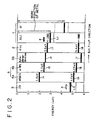
- Fig. 2 schematically shows the built-up structure of the organic EL device of this embodiment in Fig. 1 as a band model.
- upper thick lines l 1 , l 2 , l 3 and l 4 and numerical values thereof indicate the lowest unoccupied molecular orbital (LUMO) levels
- lower thick lines l 5 , l 6 , l 7 and l 8 and numerical values thereof indicate the highest occupied molecular orbital (HOMO) levels, respectively.
- LUMO lowest unoccupied molecular orbital
- HOMO highest occupied molecular orbital
- the holes h charged from the transparent electrode 5 serving as an anode are moved via the hole transport layer 4.
- electrons e charged from the metal electrode 1 serving as a cathode are moved via the electron transport layer 2.
- the electrons-holes are recombined in the hole transporting luminescent layer, at which luminescence is emitted.
- the electrons e charged from the metal electrode 1 serving as a cathode has the tendency of moving toward a lower energy level, and can arrive at the hole transporting luminescent layers 4b, 4a via the lowest unoccupied molecular orbital (LUMO) levels l 1 to l 4 of the respective layers in the order of the metal electrode 1, electron transport layer 2, hole-blocking layer 33, hole transporting luminescent layer 4b and hole transporting luminescent layer 4a.
- LUMO lowest unoccupied molecular orbital
- the holes h charged from the ITO transparent electrode 5 serving as an anode has the tendency of moving toward a higher energy level, and can move to the electron transport layer 2 via the highest occupied molecular orbital (HOMO) levels l 5 to l 7 of the respective layers in the order of the hole transporting luminescent layer 4a, hole transporting luminescent layer 4b and hole-blocking layer 33.
- HOMO occupied molecular orbital
- the highest occupied molecular orbital (HOMO) level l 8 of the electron transport layer 2 is lower in energy than the highest occupied molecular orbital (HOMO) level l 7 of the hole-blocking layer 33. This makes it difficult that the charged holes h moves from the hole-blocking layer 33 toward the electron transport layer 2, and thus, they are filled in the hole-blocking layer 33.
- the holes h filled in the hole-blocking layer 33 promote the re-combination of electrons-holes at the hole transport layer 4, thereby permitting the luminescent materials of the hole transporting luminescent layers 4a, 4b or the hole transport layer 4 to emit luminescence or light.
- the provision of the hole-blocking layer 33 effectively controls the transport of the holes h in the hole-blocking layer 33 so that the electron-hole re-combination in the hole transport layer 4 is efficiently caused.
- light with a specific wavelength blue
- the hole transporting luminescent layer 4b adjoining to the hole-blocking layer 33, of the light-emitting hole transporting luminescent layers 4a, 4b, to which emission from the hole transporting luminescent layer 4a is added.
- the electron-hole re-combination takes place in the respective layers including the electron transport layer 2 and the hole transport layer 4 as resulting from the charge of electrons from the cathode electrode 1 and the charge of holes from the anode electrode 5. Accordingly, in the absence of such a hole-blocking layer 33 as set out above, the electron-hole re-combination occurs at the interface between the electron transport layer 2 and the hole transport layer 4 so that light emission with a long wavelength alone is obtained.
- the hole-blocking layer 33 as in this embodiment it is enabled to promote blue light emission while permitting the luminescent substance-containing hole transport layer 4 as an emission region.
- the hole-blocking layer 33 is provided to control the transport of the holes h. To this end, it is sufficient that the highest occupied molecular orbital (HOMO) level of the hole-blocking layer 33 is not higher than the HOMO level that is lower in energy between the HOMO levels of the hole transporting luminescent layer 4b and the electron transport layer 2, and that the lowest unoccupied molecular orbital (LUMO) level of the hole-blocking layer 33 is not lower than the LUMO level that is lower in energy and is not higher than the LUMO level that is higher in energy, between the LUMO levels of the hole transporting luminescent layer 4b and the electron transport layer 2.
- the invention is not limited to such an arrangement as set out before.
- the energy levels may not always be within such ranges as defined before, and the bathophenanthroline compound-containing layer per se may emit light or luminescence.
- the hole-blocking layer may be made of a built-up structure including a plurality of layers.
- the hole-blocking layer 33 may be formed of the bathophenanthroline derivative and/or other material, and its thickness may be changed within a range permitting its function to be maintained. More particularly, the thickness is preferably within a range of 1 ⁇ to 1,000 ⁇ (0.1 nm to 100 nm). If the thickness is too small, the hole blocking ability becomes incomplete, so that the re-combination region is liable to extend over the hole transport layer and the electron transport layer. On the contrary, when the thickness is too large, light emission may not occur due to the increase in film resistance.
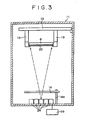
- the organic EL device 21 is made by use of a vacuum deposition apparatus 11 shown in Fig. 3 .
- the apparatus 11 has therein a pair of support means 13 fixed below an arm 12.
- a stage mechanism (not shown) is provided between the fixed support means 13 so that a transparent glass substrate 6 can be turned down and a mask 22 can be set as shown.
- a shutter 14 supported with a shaft 14a is provided below which a given number of deposition sources 28 are further provided.
- the deposition sources are heated by means of a resistance heating system using an electric power supply 29.
- an EB (electron beam) heating system may also be used, if necessary.
- the mask 22 is for pixels
- the shutter 14 is for deposition materials.
- the shutter 14 is able to rotate about the shaft 14a and has the function of intercepting a deposition stream of a material depending on the sublimation temperature of the deposition material.
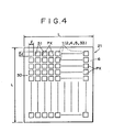
- Fig. 4 is a plan view showing a specific example of the organic EL device fabricated by use of the vacuum deposition apparatus. More particularly, ITO transparent electrodes 5 each with a size of 2 mm ⁇ 2 mm are vacuum deposited on a glass substrate 6 with a size, L, of 30 mm ⁇ 30 mm by means of the vacuum deposition apparatus in a thickness of about 100 nm, followed by vacuum deposition of SiO 2 30 over the entire surface thereof and etching in a given pixel pattern to form a multitude of openings 31. In this way, the transparent electrodes 5 are, respectively, exposed. Thereafter, the respective organic layers 4, 33, 2 and a metal electrode 1 are successively formed through a deposition mask 22 of SiO 2 on each 2 mm ⁇ 2 mm emission region (pixel) PX.
- pixel emission region
- a large-sized pixel may be singly formed, aside from the device having a multitude of pixels as shown in Fig. 4 .
- an organic EL device that is stable and high in brightness, can be driven at a low voltage and has the hole transporting luminescent layer 4.
- it is enabled to obtain a brightness of not smaller than 10,000 cd/m 2 by DC drive and a peak brightness, calculated as DC, of not smaller than 55,000 cd/m 2 by pulse drive at a duty ratio of 1/10 with respect to blue light emission.
- the transparent electrode, organic hole transport layer, organic hole-blocking layer, organic electron transport layer and metal electrode of the electroluminescent device may, respectively, have a built-up structure made of a plurality of layers.
- the respective organic layers of the electroluminescent device may be formed not only by vacuum deposition, but also other film-forming techniques using sublimation or vaporization, or a technique of spin coating, casting or the like.
- the hole transporting luminescent layer of the electroluminescent device may be formed by co-deposition of a small amount of molecules in order to control emission spectra of the device, and may be, for example, an organic thin film containing a small amount of an organic substance such as a perylene derivative, a coumarin derivative or the like.
- Usable hole transport materials include, aside from benzidine or its derivatives, styrylamine or its derivatives and triphenylmethane or its derivatives, porphyrin or its derivatives, triazole or its derivatives, imidazole or its derivatives, oxadiazole or its derivatives, polyarylalkanes or derivatives thereof, phenylenediamine or its derivatives, arylamines or derivatives thereof, oxazole or its derivatives, anthracene or its derivatives, fluorenone or its derivatives, hydrazone or its derivatives, stilbene or its derivatives, or heterocyclic conjugated monomers, oligomers, polymers and the like such as polysilane compounds, vinylcarbazole compounds, thiophene compounds, aniline compounds and the like.
- Usable electron transport materials include quinoline or its derivatives, perylene or its derivatives, bistylyl or its derivatives, pyrazine or its derivatives, and the like.
- the materials used as the anode electrode or cathode electrode of the electroluminescent device are not limitative in types.
- the cathode electrode material should preferably be made of a metal whose work function from a vacuum level of an electrode material is small in order to efficiently charge electrons.
- a metal whose work function from a vacuum level of an electrode material is small in order to efficiently charge electrons.
- low work function metals such as, for example, aluminium, indium, magnesium, silver, calcium, barium, lithium and the like, singly or in the form of alloys with other metals for enhancing the stability thereof.
- ITO In order to take out organic electroluminescence from the side of the anode electrode, ITO is used as a transparent anode electrode in examples appearing hereinafter. Nevertheless, there may be used electrode materials, which have a great work function from the vacuum level of an anode electrode material and include, for example, gold, a stannic oxide-antimony mixture, a zinc oxide-aluminium mixture or the like, so as to efficiently charge holes.
- the substrate 2 may not be limited to a glass substrate, but may be made of an opaque material. More particularly, there may be used, for example, a silicon substrate, a Cr substrate, or a substrate made of glass, on which a metal is formed by vacuum deposition. Where a substrate made of an opaque material is used, it is preferred that the upper surface of an organic EL device (i.e. the side of the cathode electrode) is formed of a transparent or translucent material so that electroluminescence is picked out to outside. ITO may be used for this purpose, for example.
- an organic EL device for full color or multi-color which is capable of emission of primaries of R, G and B, by proper choice of luminescent materials, not to mention an organic EL device for monochrome.
- the organic EL device of the invention is usable not only for display, but also for light source along with its application to other optical use.
- the organic EL device may be sealed with germanium oxide or the like so as to enhance the stability thereof by suppressing the influence of oxygen or the like in air, or may be driven under conditions drawn to vacuum.
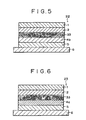
- Fig. 5 is a schematic sectional view showing an essential part of an organic EL device according to a second embodiment of the invention.
- An organic EL device 22 of this embodiment differs from that of Fig. 1 in that the hole transporting luminescent layer 4b is formed on the ITO transparent electrode 5 so that the hole transporting luminescent layer is formed as a single layer.
- Fig. 6 is a schematic sectional view showing an essential part of an organic EL device according to a third embodiment of the invention.
- An organic EL device 23 of this embodiment differs from that of Fig. 1 in that a hole transport layer (serving also as a hole transporting luminescent layer) 4a is formed on the ITO transparent electrode 5, and thus, the hole transporting luminescent layer is formed as a single layer, like the second embodiment.
- a hole transport layer serving also as a hole transporting luminescent layer 4a is formed on the ITO transparent electrode 5, and thus, the hole transporting luminescent layer is formed as a single layer, like the second embodiment.
- the invention is more particularly described by way of examples.
- n-Butyl lithium (1.6 M n-hexane solution, 17.0 ml, 26.8 mmol) was gradually dropped in an n-hexane solution (40 ml) of 2-iodotoluene (5.84 g, 26.4 mmol) at room temperature. After completion of the dropping, the reaction solution was agitated at room temperature for 16 hours, and the resultant product was separated by filtration, followed by washing of the resulting white solid with n-hexane (40 ml ⁇ 3 times).
- a toluene solution (50 ml) of bathophenanthroline (2.03 g, 6.11 mmol) was gradually dropped, at room temperature, in an anhydrous diethyl ether/toluene (3:1) solution (20 ml) of the resulting white solid, followed by agitation at room temperature for 16 hours.
- the visible light absorption maximum wavelength of a tetrahydrofuran (THF) solution of the product was at 297 nm, with a fluorescent wavelength being at 390 nm.
- n-Butyl lithium (1.6 M n-hexane solution, 60.2 ml, 96.3 mmol) was gradually dropped in an n-hexane/anhydrous diethyl ether (10:1) solution (110 ml) of 2-bromo-m-xylene (17.8 g, 96.3 mmol) at room temperature. After completion of the dropping, the reaction solution was heated under reflux for 2 hours and further agitated at room temperature for 16 hours, and the resultant product was separated by filtration, followed by washing of the resulting white solids with n-hexane (50 ml ⁇ 3 times).
- a toluene solution (80 ml) of bathophenanthroline (5.09 g, 15.3 mmol) was gradually dropped, at room temperature, in an anhydrous diethyl ether solution (40 ml) of the resulting white solids. After completion of the dropping, the solution was heated under reflux for 2 hours and agitated at room temperature for 16 hours.
- the product was identified through 1 H-NMR and FAB-MS measurements.
- the visible light absorption maximum wavelength of a THF solution of the product was at 286 nm, with a fluorescent wavelength being at 380 nm.
- n-Butyl lithium (1.6 M n-hexane solution, 15.3 ml, 24.4 mmol) was gradually dropped, at 0°C, in an n-hexane/anhydrous diethyl ether (1:1) solution (60 ml) of 1-bromonaphthalene (5.01 g, 24.4 mmol). After completion of the dropping, the reaction solution was agitated at room temperature for 16 hours, and the resultant product was subsequently separated by filtration, and the residue was washed with n-hexane (40 ml ⁇ 3 times).
- a toluene solution (80 ml) of bathophenanthroline (2.03 g, 6.11 mmol) was gradually dropped, at room temperature, in an anhydrous diethyl ether solution (40 ml) of the resulting solids. After completion of the dropping, the reaction solution was agitated at room temperature for 16 hours.
- the product was identified through 1 H-NMR and FAB-MS measurements.
- Lithium diisopropylamine (LDA)(1.89 g, 17.4 mmol) was added to a THF solution (30 ml) of fluorene (4.16 g, 25.0 mmol) and agitated at room temperature for 16 hours. Thereafter, the THF and diisopropylamine were removed by distillation under reduced pressure.
- a toluene solution (60 ml) of bathophenanthroline (2.03 g, 6.11 mmol) was gradually dropped in an anhydrous diethyl ether solution (20 ml) of the resultant yellow solids at room temperature. After the dropping, the reaction solution was heated under reflux for 2 hours and agitated at room temperature for 16 hours.
- the product was identified through 1 H-NMR and FAB-MS measurements.
- n-Butyl lithium (1.6 M n-hexane solution, 4.45 ml, 7.13 mmol) was gradually dropped in anhydrous toluene (2.24 g, 24.9 mmol) at room temperature.
- Me-THF (0.627 g, 7.47 mmol) was further added to the solution at -22°C in 20 minutes.
- THF (1.06 g, 14.7 mmol) was added to in 30 minutes, followed by agitation at 6 to 10°C for 16 hours.
- the product was identified through 1 H-NMR and FAB-MS measurements.
- n-Butyl lithium (1.6 M n-hexane solution, 36.3 ml, 58.0 mmol) was gradually dropped, at room temperature, in an n-hexane/anhydrous diethyl ether (10:1) solution (50 ml) of chlorocyclohexane (3.00 g, 25.0 mmol). After completion of the dropping, the reaction solution was further agitated at room temperature for 16 hours, and the resultant product was subsequently separated by filtration, and the resulting white solids were washed with n-hexane (50 ml ⁇ 3 times).
- a toluene solution (40 ml) of bathophenanthroline (2.03 g, 6.11 mmol) was gradually dropped, at room temperature, in an anhydrous diethyl ether solution (10 ml) of the resulting white solids. After completion of the dropping, the reaction solution was agitated at room temperature for 16 hours.
- the product was identified through 1 H-NMR and FAB-MS measurements.
- n-Butyl lithium (1.6 M n-hexane solution, 17.0 ml, 27.2 mmol) was gradually dropped, at room temperature, in an n-hexane/anhydrous diethyl ether (10:1) solution (110 ml) of 4-boromobiphenyl (6.33 g, 27.2 mmol). After completion of the dropping, the reaction solution was agitated at room temperature for 16 hours, and the resultant product was subsequently separated by filtration, and the resulting white solids were washed with n-hexane (50 ml ⁇ 3 times).
- a toluene solution (40 ml) of bathophenanthroline (2.03 g, 6.11 mmol) was gradually dropped, at room temperature, in an anhydrous diethyl ether solution (20 ml) of the resulting white solids. After completion of the dropping, the reaction solution was agitated at room temperature for 16 hours.
- the product was identified through 1 H-NMR and FAB-MS measurements.
- n-Butyl lithium (1.6 M n-hexane solution, 4.45 ml, 7.13 mmol) was gradually dropped in ⁇ -bromo-o-xylene (4.91 g, 24.9 mmol) at room temperature.
- Me-THF (0.627 g, 7.47 mmol) was added in 20 minutes at -22°C, after which THF (1.06 g, 14.7 mmol) was further added in 30 minutes, followed by further agitation at 6 to 10°C for 16 hours.
- a toluene solution (40 ml) of bathophenanthroline (2.03 g, 6.11 mmol) was gradually dropped in the resultant reaction solution at room temperature. After completion of the dropping, the reaction solution was agitated at room temperature for 16 hours.
- the product was identified through 1 H-NMR and FAB-MS measurements.
- n-Butyl lithium (1.6 M n-hexane solution, 15.3 ml, 24.4 mmol) was gradually dropped, at 0°C, in an n-hexane/anhydrous diethyl ether (1:1) solution (60 ml) of 1-bromo-8-methylnaphthalene (5.34 g, 24.4 mmol).
- the reaction solution was agitated at room temperature for 16 hours, and the resultant product was subsequently separated by filtration, and the residue was washed with n-hexane (40 ml ⁇ 3 times).
- a toluene solution (80 ml) of bathophenanthroline (2.03 g, 6.11 mmol) was gradually dropped, at room temperature, in an anhydrous diethyl ether solution (40 ml) of the resulting solids. After completion of the dropping, the reaction solution was agitated at room temperature for 16 hours.
- the product was identified through 1 H-NMR and FAB-MS measurements.
- n-Butyl lithium (1.6 M n-hexane solution, 15.3 ml, 24.4 mmol) was gradually dropped, at 0°C, in an n-hexane/anhydrous diethyl ether (1:1) solution (60 ml) of 1-boromo-2-methylnaphthalene (5.34 g, 24.4 mmol).
- the reaction solution was agitated at room temperature for 16 hours, and the resultant product was subsequently separated by filtration, and the residue was washed with n-hexane (40 ml ⁇ 3 times).
- a toluene solution (80 ml) of bathophenanthroline (2.03 g, 6.11 mmol) was gradually dropped, at room temperature, in an anhydrous diethyl ether solution (40 ml) of the resulting solids. After completion of the dropping, the reaction solution was agitated at room temperature for 16 hours.
- the product was identified through 1 H-NMR and FAB-MS measurements.
- n-Butyl lithium (1.6 M n-hexane solution, 4.45 ml, 7.13 mmol) was gradually dropped in 1-bromo-1-phenylethane (4.91 g, 24.9 mmol) at room temperature.
- Me-THF (0.627 g, 7.47 mmol) was added in 20 minutes at -22°C, after which THF (1.06 g, 14.7 mmol) was further added in 30 minutes, followed by further agitation at 6 to 10°C for 16 hours.
- a toluene solution (40 ml) of bathophenanthroline (2.03 g, 6.11 mmol) was gradually dropped in the resultant reaction solution at room temperature. After completion of the dropping, the reaction solution was agitated at room temperature for 16 hours.
- the product was identified through 1 H-NMR and FAB-MS measurements.
- the bathophenanthroline compounds of the invention can control, for example, carrier transportability depending on the type of substituent to be introduced into the molecule, thus permitting one to utilize them as a carrier transport material of various types of organic EL devices.
- these compounds have high glass transition point and melting point and are thus stable electrically, thermally and/or chemically.
- the compounds are sublimable in nature, thus leading to the advantage that they are be readily formed as a uniform amorphous film according to a vacuum deposition process.
- the bathophenanthroline compound of the invention can be efficiently prepared through nucleophilic substitution reaction using an organolithium compound.
Applications Claiming Priority (2)
| Application Number | Priority Date | Filing Date | Title |
|---|---|---|---|
| JP31207199A JP2001131174A (ja) | 1999-11-02 | 1999-11-02 | バソフェナントロリン化合物及びその製造方法 |
| JP31207199 | 1999-11-02 |
Publications (3)
| Publication Number | Publication Date |
|---|---|
| EP1097980A2 EP1097980A2 (en) | 2001-05-09 |
| EP1097980A3 EP1097980A3 (en) | 2003-09-24 |
| EP1097980B1 true EP1097980B1 (en) | 2012-07-04 |
Family
ID=18024892
Family Applications (1)
| Application Number | Title | Priority Date | Filing Date |
|---|---|---|---|
| EP00123668A Expired - Lifetime EP1097980B1 (en) | 1999-11-02 | 2000-10-30 | Bathophenanthroline compound and process for preparing same |
Country Status (3)
| Country | Link |
|---|---|
| US (4) | US6972334B1 (US20040265626A1-20041230-C00025.png) |
| EP (1) | EP1097980B1 (US20040265626A1-20041230-C00025.png) |
| JP (1) | JP2001131174A (US20040265626A1-20041230-C00025.png) |
Cited By (2)
| Publication number | Priority date | Publication date | Assignee | Title |
|---|---|---|---|---|
| US8420229B2 (en) | 2007-10-26 | 2013-04-16 | Global OLED Technologies LLC | OLED device with certain fluoranthene light-emitting dopants |
| US8431242B2 (en) | 2007-10-26 | 2013-04-30 | Global Oled Technology, Llc. | OLED device with certain fluoranthene host |
Families Citing this family (48)
| Publication number | Priority date | Publication date | Assignee | Title |
|---|---|---|---|---|
| JP4876311B2 (ja) * | 2000-01-14 | 2012-02-15 | 東レ株式会社 | 発光素子 |
| US6664111B2 (en) * | 2001-08-22 | 2003-12-16 | 3M Innovative Properties Company | Fluorescence based oxygen sensor systems |
| JP4261855B2 (ja) | 2002-09-19 | 2009-04-30 | キヤノン株式会社 | フェナントロリン化合物及びそれを用いた有機発光素子 |
| JP4001118B2 (ja) | 2003-03-24 | 2007-10-31 | ソニー株式会社 | 有機電界発光素子及びアミノモノスチリルナフタレン化合物 |
| JP3890317B2 (ja) | 2003-04-30 | 2007-03-07 | キヤノン株式会社 | 発光素子 |
| US7750159B2 (en) | 2004-07-07 | 2010-07-06 | Semiconductor Energy Laboratory Co., Ltd. | Phenanthroline derivative and light emitting element and light emitting device using the same |
| BRPI0516786A (pt) * | 2004-11-24 | 2008-09-23 | Univ Princeton | dispositivo optoeletrÈnico fotosensìvel orgánico tendo uma camada bloqueadora de éxcitons de fenantrolina |
| JP2006151866A (ja) | 2004-11-29 | 2006-06-15 | Canon Inc | フェナントロリン化合物及び発光素子 |
| US7714501B2 (en) * | 2004-12-01 | 2010-05-11 | Semiconductor Energy Laboratory Co., Ltd. | Light emitting element, light emitting device and electronic equipment |
| JP4865258B2 (ja) | 2005-06-21 | 2012-02-01 | キヤノン株式会社 | 1,8−ナフチリジン化合物及びそれを用いた有機発光素子 |
| JP5317386B2 (ja) * | 2005-08-05 | 2013-10-16 | 出光興産株式会社 | 含窒素複素環誘導体及びそれを用いた有機エレクトロルミネッセンス素子 |
| JP4842587B2 (ja) * | 2005-08-11 | 2011-12-21 | 株式会社半導体エネルギー研究所 | フェナントロリン誘導体化合物、並びにそれを利用する電子輸送性材料、発光素子、発光装置及び電子機器 |
| DE502005009802D1 (de) * | 2005-11-10 | 2010-08-05 | Novaled Ag | Dotiertes organisches Halbleitermaterial |
| US7919010B2 (en) * | 2005-12-22 | 2011-04-05 | Novaled Ag | Doped organic semiconductor material |
| ES2310380T3 (es) | 2006-03-21 | 2009-01-01 | Novaled Ag | Radical o dirradical heterociclicos, sus dimeros, oligomeros, polimeros, compuestos diespiro y policiclos, su utilizacion, material semiconductor organico asi como componente electronico. |
| EP1837927A1 (de) * | 2006-03-22 | 2007-09-26 | Novaled AG | Verwendung von heterocyclischen Radikalen zur Dotierung von organischen Halbleitern |
| CN101461073B (zh) * | 2006-06-01 | 2013-01-02 | 株式会社半导体能源研究所 | 发光元件、发光器件和电子器件 |
| US9397308B2 (en) * | 2006-12-04 | 2016-07-19 | Semiconductor Energy Laboratory Co., Ltd. | Light emitting element, light emitting device, and electronic device |
| DE102007012794B3 (de) | 2007-03-16 | 2008-06-19 | Novaled Ag | Pyrido[3,2-h]chinazoline und/oder deren 5,6-Dihydroderivate, deren Herstellungsverfahren und diese enthaltendes dotiertes organisches Halbleitermaterial |
| DE102007018456B4 (de) * | 2007-04-19 | 2022-02-24 | Novaled Gmbh | Verwendung von Hauptgruppenelementhalogeniden und/oder -pseudohalogeniden, organisches halbleitendes Matrixmaterial, elektronische und optoelektronische Bauelemente |
| US7754348B2 (en) | 2007-04-25 | 2010-07-13 | Luminescene Technology Corp. | Phenanthroline compound and organic light emitting device using the same |
| EP1988587B1 (de) | 2007-04-30 | 2016-12-07 | Novaled GmbH | Oxokohlenstoff-, Pseudooxokohlenstoff- und Radialenverbindungen sowie deren Verwendung |
| EP1990847B1 (de) * | 2007-05-10 | 2018-06-20 | Novaled GmbH | Verwendung von chinoiden Bisimidazolen und deren Derivaten als Dotand zur Dotierung eines organischen halbleitenden Matrixmaterials |
| TW200906218A (en) * | 2007-05-16 | 2009-02-01 | Yamagata Promotional Org Ind | Electron transporting materials and organic light-emitting devices therewith |
| DE102007031220B4 (de) | 2007-07-04 | 2022-04-28 | Novaled Gmbh | Chinoide Verbindungen und deren Verwendung in halbleitenden Matrixmaterialien, elektronischen und optoelektronischen Bauelementen |
| US8076009B2 (en) | 2007-10-26 | 2011-12-13 | Global Oled Technology, Llc. | OLED device with fluoranthene electron transport materials |
| WO2009081857A1 (ja) | 2007-12-21 | 2009-07-02 | Idemitsu Kosan Co., Ltd. | 有機エレクトロルミネッセンス素子 |
| KR100901887B1 (ko) * | 2008-03-14 | 2009-06-09 | (주)그라쎌 | 신규한 유기 발광 화합물 및 이를 채용하고 있는 유기 발광소자 |
| US8057712B2 (en) * | 2008-04-29 | 2011-11-15 | Novaled Ag | Radialene compounds and their use |
| EP2161272A1 (en) | 2008-09-05 | 2010-03-10 | Basf Se | Phenanthrolines |
| US7931975B2 (en) | 2008-11-07 | 2011-04-26 | Global Oled Technology Llc | Electroluminescent device containing a flouranthene compound |
| US8088500B2 (en) | 2008-11-12 | 2012-01-03 | Global Oled Technology Llc | OLED device with fluoranthene electron injection materials |
| US7968215B2 (en) | 2008-12-09 | 2011-06-28 | Global Oled Technology Llc | OLED device with cyclobutene electron injection materials |
| JP5591822B2 (ja) * | 2008-12-12 | 2014-09-17 | イー・アイ・デュポン・ドウ・ヌムール・アンド・カンパニー | 光活性組成物、および、この組成物で形成された電子素子 |
| US8278651B2 (en) * | 2008-12-22 | 2012-10-02 | E I Du Pont De Nemours And Company | Electronic device including 1,7-phenanthroline derivative |
| EP2361009A4 (en) | 2008-12-22 | 2012-12-05 | Du Pont | ELECTRONIC DEVICE WITH A PHENANTHROLINE DERIVATIVE |
| US8471247B2 (en) * | 2009-08-24 | 2013-06-25 | E I Du Pont De Nemours And Company | Organic light-emitting diode luminaires |
| JP5102818B2 (ja) * | 2009-09-29 | 2012-12-19 | 独立行政法人科学技術振興機構 | フェナントロリン誘導体を用いた光電変換素子およびその製造方法 |
| US8617720B2 (en) | 2009-12-21 | 2013-12-31 | E I Du Pont De Nemours And Company | Electroactive composition and electronic device made with the composition |
| EP2381502B1 (en) * | 2010-04-23 | 2013-08-14 | Novaled AG | Organic semiconducting layer |
| KR102244374B1 (ko) | 2013-08-09 | 2021-04-26 | 가부시키가이샤 한도오따이 에네루기 켄큐쇼 | 발광 소자, 디스플레이 모듈, 조명 모듈, 발광 장치, 표시 장치, 전자 기기, 및 조명 장치 |
| TWI727366B (zh) | 2013-08-09 | 2021-05-11 | 日商半導體能源研究所股份有限公司 | 發光元件、顯示模組、照明模組、發光裝置、顯示裝置、電子裝置、及照明裝置 |
| CN104059065B (zh) * | 2014-05-30 | 2017-01-04 | 浙江工业大学 | 一种邻菲咯啉衍生物及其制备方法与应用 |
| GB2528906A (en) * | 2014-08-04 | 2016-02-10 | Novaled Gmbh | Organic light emitting devices and methods |
| JP2016082239A (ja) | 2014-10-16 | 2016-05-16 | 株式会社半導体エネルギー研究所 | 発光素子、発光装置、電子機器及び照明装置 |
| KR20160087433A (ko) * | 2015-01-13 | 2016-07-22 | 삼성디스플레이 주식회사 | 유기발광소자 및 이를 갖는 표시장치 |
| EP3147961A1 (en) * | 2015-09-28 | 2017-03-29 | Novaled GmbH | Organic electroluminescent device |
| CN106866660B (zh) * | 2017-02-15 | 2019-05-17 | 上海天马有机发光显示技术有限公司 | 电子传输材料、包含其的oled显示面板和电子设备 |
Family Cites Families (7)
| Publication number | Priority date | Publication date | Assignee | Title |
|---|---|---|---|---|
| US3951833A (en) * | 1975-02-27 | 1976-04-20 | Olin Corporation | Method for preserving functional fluids and liquid hydrocarbon fuels with selected 1,10-phenanthrolines |
| US4853090A (en) * | 1988-04-28 | 1989-08-01 | Eastman Kodak Company | Lithium ion-selective compositions, electrodes and a method of use |
| US5077142A (en) | 1989-04-20 | 1991-12-31 | Ricoh Company, Ltd. | Electroluminescent devices |
| EP0493745A1 (en) * | 1990-12-21 | 1992-07-08 | Dojindo Laboratories | Fluorescent compound, complex, reagent, and specific binding assay employing said reagent |
| US5393614A (en) * | 1992-04-03 | 1995-02-28 | Pioneer Electronic Corporation | Organic electroluminescence device |
| US6312836B1 (en) | 1998-04-10 | 2001-11-06 | The Trustees Of Princeton University | Color-tunable organic light emitting devices |
| JP3924648B2 (ja) * | 1999-11-02 | 2007-06-06 | ソニー株式会社 | 有機電界発光素子 |
-
1999
- 1999-11-02 JP JP31207199A patent/JP2001131174A/ja active Pending
-
2000
- 2000-10-30 EP EP00123668A patent/EP1097980B1/en not_active Expired - Lifetime
- 2000-11-02 US US09/704,968 patent/US6972334B1/en not_active Expired - Fee Related
-
2003
- 2003-09-05 US US10/656,659 patent/US20050073641A1/en not_active Abandoned
-
2004
- 2004-03-11 US US10/798,820 patent/US7186469B2/en not_active Expired - Fee Related
-
2005
- 2005-02-21 US US11/062,076 patent/US20050154208A1/en not_active Abandoned
Cited By (2)
| Publication number | Priority date | Publication date | Assignee | Title |
|---|---|---|---|---|
| US8420229B2 (en) | 2007-10-26 | 2013-04-16 | Global OLED Technologies LLC | OLED device with certain fluoranthene light-emitting dopants |
| US8431242B2 (en) | 2007-10-26 | 2013-04-30 | Global Oled Technology, Llc. | OLED device with certain fluoranthene host |
Also Published As
| Publication number | Publication date |
|---|---|
| US20040265626A1 (en) | 2004-12-30 |
| EP1097980A2 (en) | 2001-05-09 |
| EP1097980A3 (en) | 2003-09-24 |
| US20050154208A1 (en) | 2005-07-14 |
| US6972334B1 (en) | 2005-12-06 |
| JP2001131174A (ja) | 2001-05-15 |
| US7186469B2 (en) | 2007-03-06 |
| US20050073641A1 (en) | 2005-04-07 |
Similar Documents
| Publication | Publication Date | Title |
|---|---|---|
| EP1097980B1 (en) | Bathophenanthroline compound and process for preparing same | |
| EP1097981B1 (en) | Organic electroluminescent device | |
| JP4032566B2 (ja) | 発光素子 | |
| EP2415752B1 (en) | Aromatic amine derivative and organic electroluminescent element using same | |
| TWI378984B (en) | Light-emitting element material and light-emitting element | |
| JP4843889B2 (ja) | 発光素子 | |
| WO2002043449A1 (fr) | Materiau luminescent et element luminescent contenant celui-ci | |
| JP4103493B2 (ja) | 有機エレクトロルミネッセンス素子および表示装置 | |
| EP0929104B1 (en) | Electroluminescence device and process for producing the same | |
| KR20010093121A (ko) | 유기 전기발광 소자 | |
| JP2001023777A (ja) | 発光素子 | |
| JP2004204140A (ja) | 発光素子用材料およびそれを用いた発光素子 | |
| JPH10183112A (ja) | 電界発光素子 | |
| JP4918810B2 (ja) | 置換フェニルエチニル銅−含窒素へテロ環カルベン錯体及びそれを用いた有機エレクトロルミネッセンス素子 | |
| JP4590678B2 (ja) | 発光素子 | |
| JP3970495B2 (ja) | 有機el素子 | |
| JP2002326965A (ja) | スピロフルオレン化合物及びその製造方法、並びにその合成中間体、及びそのスピロフルオレン化合物を用いた有機電界発光素子 | |
| JPH10284252A (ja) | 有機el素子 | |
| JP3891858B2 (ja) | 有機電界発光素子 | |
| JP2004203828A (ja) | ホスフィンオキサイド化合物およびそれを用いた発光素子用材料ならびに発光素子 | |
| JP5099409B2 (ja) | アリールシラン化合物とその用途 | |
| JP4048645B2 (ja) | 発光素子 | |
| JP2003249372A (ja) | 有機電界発光素子 | |
| WO2005005408A1 (ja) | アミン化合物とその用途 | |
| JP2004043646A (ja) | 有機電界発光素子 |
Legal Events
| Date | Code | Title | Description |
|---|---|---|---|
| PUAI | Public reference made under article 153(3) epc to a published international application that has entered the european phase |
Free format text: ORIGINAL CODE: 0009012 |
|
| AK | Designated contracting states |
Kind code of ref document: A2 Designated state(s): AT BE CH CY DE DK ES FI FR GB GR IE IT LI LU MC NL PT SE |
|
| AX | Request for extension of the european patent |
Free format text: AL;LT;LV;MK;RO;SI |
|
| PUAL | Search report despatched |
Free format text: ORIGINAL CODE: 0009013 |
|
| RIC1 | Information provided on ipc code assigned before grant |
Ipc: 7H 01L 51/30 B Ipc: 7C 07D 471/04 B Ipc: 7C 09K 11/06 A |
|
| AK | Designated contracting states |
Kind code of ref document: A3 Designated state(s): AT BE CH CY DE DK ES FI FR GB GR IE IT LI LU MC NL PT SE |
|
| AX | Request for extension of the european patent |
Extension state: AL LT LV MK RO SI |
|
| 17P | Request for examination filed |
Effective date: 20040226 |
|
| AKX | Designation fees paid |
Designated state(s): DE FR GB |
|
| GRAP | Despatch of communication of intention to grant a patent |
Free format text: ORIGINAL CODE: EPIDOSNIGR1 |
|
| GRAS | Grant fee paid |
Free format text: ORIGINAL CODE: EPIDOSNIGR3 |
|
| RIN1 | Information on inventor provided before grant (corrected) |
Inventor name: TAMURA, SHINICHIRO Inventor name: ASAI, NOBUTOSHI Inventor name: KIJIMA, YASUNORI Inventor name: SHIBANUMA, TETSUO |
|
| GRAA | (expected) grant |
Free format text: ORIGINAL CODE: 0009210 |
|
| RAP1 | Party data changed (applicant data changed or rights of an application transferred) |
Owner name: SONY CORPORATION |
|
| AK | Designated contracting states |
Kind code of ref document: B1 Designated state(s): DE FR GB |
|
| REG | Reference to a national code |
Ref country code: GB Ref legal event code: FG4D |
|
| REG | Reference to a national code |
Ref country code: DE Ref legal event code: R096 Ref document number: 60047309 Country of ref document: DE Effective date: 20120823 |
|
| PGFP | Annual fee paid to national office [announced via postgrant information from national office to epo] |
Ref country code: FR Payment date: 20121031 Year of fee payment: 13 Ref country code: DE Payment date: 20121023 Year of fee payment: 13 |
|
| PGFP | Annual fee paid to national office [announced via postgrant information from national office to epo] |
Ref country code: GB Payment date: 20121019 Year of fee payment: 13 |
|
| PLBE | No opposition filed within time limit |
Free format text: ORIGINAL CODE: 0009261 |
|
| STAA | Information on the status of an ep patent application or granted ep patent |
Free format text: STATUS: NO OPPOSITION FILED WITHIN TIME LIMIT |
|
| 26N | No opposition filed |
Effective date: 20130405 |
|
| REG | Reference to a national code |
Ref country code: DE Ref legal event code: R097 Ref document number: 60047309 Country of ref document: DE Effective date: 20130405 |
|
| GBPC | Gb: european patent ceased through non-payment of renewal fee |
Effective date: 20131030 |
|
| REG | Reference to a national code |
Ref country code: DE Ref legal event code: R119 Ref document number: 60047309 Country of ref document: DE Effective date: 20140501 |
|
| PG25 | Lapsed in a contracting state [announced via postgrant information from national office to epo] |
Ref country code: GB Free format text: LAPSE BECAUSE OF NON-PAYMENT OF DUE FEES Effective date: 20131030 |
|
| REG | Reference to a national code |
Ref country code: FR Ref legal event code: ST Effective date: 20140630 |
|
| PG25 | Lapsed in a contracting state [announced via postgrant information from national office to epo] |
Ref country code: DE Free format text: LAPSE BECAUSE OF NON-PAYMENT OF DUE FEES Effective date: 20140501 Ref country code: FR Free format text: LAPSE BECAUSE OF NON-PAYMENT OF DUE FEES Effective date: 20131031 |