EP1096576B1 - Semiconductor device - Google Patents
Semiconductor device Download PDFInfo
- Publication number
- EP1096576B1 EP1096576B1 EP00113802A EP00113802A EP1096576B1 EP 1096576 B1 EP1096576 B1 EP 1096576B1 EP 00113802 A EP00113802 A EP 00113802A EP 00113802 A EP00113802 A EP 00113802A EP 1096576 B1 EP1096576 B1 EP 1096576B1
- Authority
- EP
- European Patent Office
- Prior art keywords
- semiconductor layer
- layer
- semiconductor
- electrode
- sandwiched
- Prior art date
- Legal status (The legal status is an assumption and is not a legal conclusion. Google has not performed a legal analysis and makes no representation as to the accuracy of the status listed.)
- Expired - Lifetime
Links
Images


Classifications
-
- H—ELECTRICITY
- H10—SEMICONDUCTOR DEVICES; ELECTRIC SOLID-STATE DEVICES NOT OTHERWISE PROVIDED FOR
- H10D—INORGANIC ELECTRIC SEMICONDUCTOR DEVICES
- H10D8/00—Diodes
- H10D8/50—PIN diodes
-
- H—ELECTRICITY
- H10—SEMICONDUCTOR DEVICES; ELECTRIC SOLID-STATE DEVICES NOT OTHERWISE PROVIDED FOR
- H10D—INORGANIC ELECTRIC SEMICONDUCTOR DEVICES
- H10D62/00—Semiconductor bodies, or regions thereof, of devices having potential barriers
- H10D62/60—Impurity distributions or concentrations
Definitions
- the present invention relates to semiconductor devices having a pin structure, such as diodes, transistors, thyristors, etc.
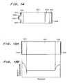
- Figs.15A, 15B show the structure of a conventional pin diode, where Fig.15A shows its cross section and Fig.15B shows its impurity concentration profile.
- the n - -type semiconductor substrate 601 mainly composed of silicon, for example, has a p layer 602 on one of its main surfaces (on the left in the drawing) and an n + layer 603 on the other main surface (on the right in the drawing).
- the p layer 602 contains boron or gallium as an impurity and the n + layer 603 contains phosphorus, which are obtained by diffusing the impurity to a given depth by thermal treatment.
- the p layer 602 and the n + layer 603 respectively have an anode electrode 604 and a cathode electrode 605 made of an electrically low resistant metal on the opposite sides to the n - -type semiconductor substrate 601.
- the impurity in the n - -type semiconductor substrate 601 is almost uniformly distributed with a very small impurity concentration gradient. Since the p layer 602 and the n + layer 603 are formed by applying impurity diffusion to the two main surfaces of the n - -type semiconductor substrate 601, the impurity concentration in each layer has an impurity concentration gradient decreasing toward the n - -type semiconductor substrate 601. For example, the n + layer 603 has an impurity concentration gradient of about 4 ⁇ 10 18 cm -4 .
- the impurity concentration gradient is given as a value obtained by dividing the difference between a first concentration that is 90 % of the maximum value of the impurity concentration in the n + layer 603 and a second concentration that is 50 % of the maximum value by the distance from the position having the first concentration to the position having the second concentration.
- a center of carrier recombination is formed by proton irradiation etc. in the vicinity of the pn junction formed by the p layer 602 and the n - -type semiconductor substrate 601 so as to locally shorten the lifetime in the vicinity of the pn junction, thus providing a characteristic with lower forward voltage, smaller reverse recovery current, and high di/dt tolerance.
- the entirety of the n - -type semiconductor substrate 601 is subjected to diffusion of heavy metal, irradiation of electron beam etc. to set the carrier lifetime short.
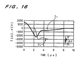
- Fig.16 is a graph showing the time variation in voltage V A and current I A during the reverse recovery operation of the diode shown in Fig.15 , where the time at which the forward bias is switched to the reverse bias by an external circuit is set as zero.
- the current of the diode becomes steady zero when about 8 ⁇ s passed after the switching and a voltage oscillation having an amplitude ⁇ V exceeding 2000 V occurs immediately after that.
- the LCR series circuit is formed of a capacitance component C defined by the depletion layer and excess carriers of the diode as parameters, a resistance component R defined by the applied voltage and leakage current of the diode and the recombination current of the excess carriers as parameters, and the inductance component L of the external circuit.
- the capacitance component C and the resistance component R of the diode change with time. Especially, the resistance component R rapidly changes when the excess carriers outside the depletion layer disappear. Then the resonance condition of the LCR circuit is reached and the voltage will oscillate as shown in Fig.16 . When the depletion layer reaches the n + layer 603, the capacitance component C rapidly changes, which may trigger the voltage oscillation.
- Such voltage oscillation can occur not only in diodes but also in GCT (gate controlled turn-off) thyristors with rapid switching rate when the voltage rises in turn-off operation. Such voltage oscillation is undesired because it causes such noise as may cause malfunction of the peripheral electric equipment.
- GCT gate controlled turn-off
- Japanese Patent Laying-open No. 62-115880 discloses a technique for controlling the semiconductor layer and concentration to improve the waveform in reverse recovery operation.
- EP 0 749 166 and US 4 951 109 are considered as the closest prior art, and comprise all of the features of the preamble of claim 1.
- a first aspect of the present invention is directed to a semiconductor device having a PIN structure comprising a first semiconductor layer of a first conductivity type, a second semiconductor layer of a second conductivity type, and a semiconductor substrate which is interposed between the first semiconductor layer and the second semiconductor layer and has the second conductivity type with an impurity concentration lower than that in the second semiconductor layer.
- the second semiconductor layer has an impurity concentration decreasing toward the semiconductor substrate, and the impurity concentration in the second semiconductor layer decreases from 90 % of its maximum value to 50 % thereof at an impurity concentration gradient equal to or less than 2 ⁇ 10 18 cm -4 .
- the maximum value of the impurity concentration in the second semiconductor layer is not more than 5 ⁇ 10 15 cm -3 .
- the semiconductor device further comprises a third semiconductor layer of the second conductivity type formed so that the second semiconductor layer is sandwiched between the semiconductor substrate and the third semiconductor layer, and a metal electrode formed so that the third semiconductor layer is sandwiched between the second semiconductor layer and the metal electrode, wherein the third semiconductor layer has a surface impurity concentration of not less than 5 ⁇ 10 17 cm -3 on the side of the metal electrode.
- the ratio of the amount of impurity in the semiconductor substrate to the amount of impurity in the first semiconductor layer is not more than 2/3.
- the ratio of the amount of impurity in the second semiconductor layer to the amount of impurity in the first semiconductor layer is not less than 1.
- the ratio of the amount of impurity in the second semiconductor layer to the amount of impurity in the first semiconductor layer is not less than 3/2.
- the second semiconductor layer has a gentle impurity concentration gradient, which suppresses rapid expansion of the depletion layer in reverse recovery operation of a diode having the pn junction formed by the first semiconductor layer and the semiconductor substrate and in turn-off operation of a transistor or a GCT thyristor having the pn junction. Accordingly, it is possible to suppress unwanted voltage variation in the above-mentioned operations, or generation of noise.
- the impurity concentration gradient mentioned in the first aspect can be obtained easily.
- the presence of the third semiconductor layer having high impurity concentration provides good ohmic contact between the metal electrode and the second semiconductor layer.
- the semiconductor device of the fourth aspect can be formed thinner to realize smaller on-state voltage.
- the semiconductor device of the fifth aspect it is possible to reduce the leakage current.
- the leakage current can be 10 mA or smaller.
- the present invention has been made to solve the problems described above, and an object of the present invention is to provide a semiconductor device in which oscillation of the applied voltage is small in the reverse recovery operation or turn-off operation.
- Figs.1A, 1B show the structure of a pin diode according to a first preferred embodiment of the present invention, where Fig.1A shows its cross section and Fig.1B shows its impurity concentration profile.
- the n - -type semiconductor substrate 101 mainly composed of silicon, for example, has a p layer 102 on one of its main surfaces (on the left in the drawing) and an n + layer 103 on the other main surface (on the right in the drawing).
- the p layer 102 contains boron or gallium as an impurity and the n + layer 103 contains phosphorus, which are obtained by diffusing the impurity to a given depth by thermal treatment.
- the p layer 102 and the n + layer 103 respectively have an anode electrode 104 and a cathode electrode 105 made of electrically low resistant metal on the opposite sides to the n - -type semiconductor substrate 101.
- the center of carrier recombination is formed by proton irradiation etc. in the vicinity of the pn junction formed by the p layer 102 and the n - -type semiconductor substrate 101 so as to locally shorten the lifetime in the vicinity of the pn junction, thus providing a characteristic with low forward voltage, small reverse recovery current, and high di/dt tolerance.
- the entirety of the n - -type semiconductor substrate 101 is subjected to diffusion of heavy metal, irradiation of electron beam, to shorten the carrier lifetime.
- the impurity in the n - -type semiconductor substrate 101 is almost uniformly distributed with a very small impurity concentration gradient. Since the p layer 102 and the n + layer 103 are formed by applying impurity diffusion to the two main surfaces of the n - -type semiconductor substrate 101, the impurity concentration in each layer has an impurity concentration gradient decreasing toward the n - -type semiconductor substrate 101.
- the n + layer 103 has an impurity concentration gradient equal to or less than 2 ⁇ 10 18 cm -4 .
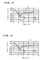
- Figs.2 and 3 are graphs showing the time variation in the voltage V A and the current I A during the reverse recovery operation of the diode shown in Figs.1A, 1B , where the time at which the forward bias is switched to the reverse bias by an external circuit is set as zero.
- Figs.2 and 3 show examples in which the impurity concentration gradient in the n + layer 103 is set to 2 ⁇ 10 18 cm -4 and 9 ⁇ 10 17 cm -4 , respectively, where the distance between the anode electrode 104 and the cathode electrode 105, the total amount of impurity introduced in the n + layer 103, and the thickness and impurity profile of the p layer 102 are set equal to those in the example shown in Fig.16 .
- Fig.4 is a graph showing the relation between the impurity concentration gradient in the n + layer 103 and the amplitude ⁇ V of the voltage oscillation in the reverse recovery operation, where ⁇ shows actual measurements. It can be seen from the graph that the voltage oscillation during the reverse recovery operation decreases as the impurity concentration gradient in the n + layer 103 becomes gentler. The reason is considered as follows: when the depletion layer extending from the pn junction reaches the n + layer 103 during the reverse recovery operation, the expansion of the depletion layer becomes less likely to stop rapidly as the impurity concentration gradient in the n + layer 103 becomes smaller.
- n + layer 103 phosphorus or arsenic is applied to the n - -type semiconductor substrate 101 by ion implantation or thermal treatment at about 1000°C and then diffused to a given depth by thermal treatment at high temperature of 1100°C or higher.
- thermal treatment at high temperature of 1100°C or higher.
- the thickness of the n + layer 103 becomes larger as the impurity concentration gradient becomes smaller.
- the n - -type semiconductor substrate 101 forms thinner as the impurity concentration gradient becomes smaller.
- the distance between the anode electrode 104 and the cathode electrode 105 which is approximately equal to the thickness of the n - -type semiconductor substrate 101 before formation of the p layer 102 and the n + layer 103, the total amount of impurity introduced in the n + layer 103, and the thickness and impurity profile of the p layer 102 are fixed, the n - -type semiconductor substrate 101 becomes thinner as the impurity concentration gradient becomes smaller, and then the depletion layer reaches the n + layer 103 in shorter time.
- This is considered to be an indirect cause of the fact that the voltage oscillation during the reverse recovery operation can be alleviated by setting the impurity concentration gradient in the n + layer 103 smaller.
- Fig.5 shows impurity concentration profiles of pin diodes, which correspond to Fig.15(b) and Fig.1(b) .
- the lines 101a and 101b represent the impurity concentration profiles in the n - -type semiconductor substrate 101
- 102a and 102b represent those in the p layer 102
- 103a and 103b represent those in the n + layer 103.
- the graph 101a, 102a, and 103a and the graph 101b, 102b, and 103b show the impurity concentration profiles in pin diodes constructed separately.
- the surface impurity concentration in the n + layer 103 at the most distant position from the n - -type semiconductor substrate 101 is set to N1 and N2 (N1 ⁇ N2), respectively.
- the n + layer 103 usually, phosphorus or arsenic is applied to the n - -type semiconductor substrate 101 by ion implantation or thermal treatment at about 1000°C and diffused to a given depth by thermal treatment at high temperature of 1100°C or higher. Accordingly, when obtaining the impurity concentration gradient in a certain n + layer 103, the n + layer 103 forms thinner in the diode having the n + layer 103 with the lower surface impurity concentration N1 than in the diode having the n + layer 103 with the higher surface impurity concentration N2. Hence, to form the n + layer 103 in a shorter time, it is desirable to set the surface impurity concentration lower.
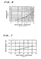
- Fig.6 is a graph showing the relation between the surface impurity concentration of the n + layer 103 and the thickness of the n + layer 103 or the diffusion depth, which shows an example in which the impurity concentration gradient in the n + layer 103 is set to 2 ⁇ 10 18 cm -4 .
- O shows actual measurements. While the diffusion depth is about 40 ⁇ m when the surface impurity concentration is 5 ⁇ 10 15 cm -3 , the diffusion depth of about 75 ⁇ m is required when the surface impurity concentration is 1 ⁇ 10 16 cm -3 .
- the diffusion time required for diffusion while about 25 hours are required at a diffusion temperature of 1250°C for the 40- ⁇ m-depth diffusion, about 85 hours are required for the 75- ⁇ m- depth diffusion.
- the impurity concentration gradient in the n + layer 103 is not more than 2 ⁇ 10 18 cm -4 as in the case of the diode of the first preferred embodiment, it is desired that the surface impurity concentration of the n + layer 103 is not more than 5 ⁇ 10 15 cm -3 and the diffusion depth is not more than 40 ⁇ m.
- Fig.7 is a graph showing the relation between the surface impurity concentration of the n + layer 103 and the reverse recovery loss for each switching.
- O shows actual measurements.
- reducing the surface impurity concentration of the n + layer 103 is desired also in respect of suppression of the loss.
- Fig.8 is a graph showing the relation between the impurity concentration in n-type semiconductor in a pin diode at a position in contact with the cathode electrode, or the surface impurity concentration, and the on-state voltage of the diode, where ⁇ represents actual measurements.
- the n-type semiconductor is mainly composed of silicon and the cathode electrode is mainly composed of aluminum. While the on-state voltage is almost constant at 3.0 V when the surface impurity concentration of the n-type semiconductor in contact with the cathode electrode is 5 ⁇ 10 17 cm -3 or higher, the on-state voltage sharply increases with a decrease in the surface impurity concentration when the surface impurity concentration is lower than 5 ⁇ 10 17 cm -3 .
- this variation depends on whether ohmic contact can be favorably made between the cathode electrode and the n-type semiconductor in contact with it. Accordingly, it is desired that the surface impurity concentration of the n-type semiconductor in a position in contact with the cathode electrode is set equal to or more than 5 ⁇ 10 17 cm -3 to obtain good ohmic contact.
- the cathode electrode 105 is in direct contact with the n + layer 103 having a low surface impurity concentration of 5 ⁇ 10 15 cm -3 or lower as described in the second preferred embodiment, it is difficult to make good ohmic contact.
- Fig.9 is a sectional view showing the structure of a pin diode according to a third preferred embodiment of the present invention.
- an n ++ layer 106 is interposed between the n + layer 103 and the cathode electrode 105 in the pin diode of the first preferred embodiment of the invention (see Fig.1(a) ).
- the value of the impurity concentration in the n + layer 103 at the most distant position from the n - -type semiconductor substrate 101, or at the closest position to the n ++ layer 106 i.e.
- the surface impurity concentration of the n + layer 103 can be set to 5 ⁇ 10 15 cm -3 or lower while the surface impurity concentration of the n ++ layer 106 is set to 5 ⁇ 10 17 cm -3 or higher, and then the impurity concentration gradient in the n + layer 103 can easily be set to 2 ⁇ 10 18 cm -4 or lower while obtaining good ohmic contact with the cathode electrode 105.
- This provides a pin diode in which the voltage amplitude appearing after the completion of the reverse recovery operation is reduced and the on-voltage is small.
- Figs.10A, 10B show diagrams used to explain this preferred embodiment, where Fig.10A shows the impurity concentration profile in a pin diode in a manner corresponding to Fig.15B and Fig.1B , and the graph 101c, 102c, and 103c shows the impurity concentration profile in the n - -type semiconductor substrate 101, the p layer 102, and the n + layer 103, respectively.
- Fig.10B shows electric field strength profiles in the pin diode exhibited when a reverse bias is applied and the rated voltage is kept, where, particularly, the graph E1 is aligned in position with Fig.10A .
- the depletion layer extending from the pn junction between the n - -type semiconductor substrate 101 and the p layer 102 reaches the n + layer 103, and the electric field strength E1 is large in the depletion layer.
- the depletion layer extends over the region A, region B, and region D.
- the region B extends in the entirety of the n - -type semiconductor substrate 101, the region A partially penetrates the p layer 102 from the position in contact with the n - -type semiconductor substrate 101, and the region D partially penetrates the n + layer 103 from the position in contact with the n - -type semiconductor substrate 101.
- the amount of impurity in the region A (hereinafter the character A is attached thereto) is not more than the sum of the amount of impurity in the region B (hereinafter the character B is attached thereto) and the amount of impurity in the region D (hereinafter the character D is attached thereto).
- the end of the region A away from the n - -type semiconductor substrate 101 is determined by the amount of impurity A and the curve 102c, and the end of the region D away from the n - -type semiconductor substrate 101 is determined by the amount of impurity D and the curve 103c.
- the rated breakdown voltage is not reduced even if fine particles etc. attach to it.
- the p layer 102 is formed much thicker than those in other types of device, which is set to about 100 ⁇ m.
- the amount of impurity A is about half of the total amount of impurity in the p layer 102 and the amount of impurity D is also about half of the amount of impurity in the n + layer 103.
- the graphs E1 and E2 show the electric field strengths in examples in which the ratio of the amount of impurity B to the amount of impurity A, i.e. the ratio B/A, is 1 and 2/3, respectively.
- the electric field strength in the latter bends in a position closer to the p layer 102, and the pin diode can be formed thinner to reduce the on-state voltage.
- B/A ⁇ 2/3 the on-state voltage takes an almost constant value of about 3V independently of the ratio B/A, but when B/A>2/3, the on-state voltage sharply increases as the ratio B/A increases.
- Fig.12 is a graph showing results of simulation about the relation between the ratio D/A of the amount of impurity D to the amount of impurity A and the leakage current, where the ratio B/A is set to 2/3.
- Fig.13 is a sectional view showing the structure of a transistor having the pin structure.
- the transistor has a p layer 402, an n + layer 403, an n - layer 401 interposed between the p layer 402 and the n + layer 403, a p + layer 404 formed so that the n + layer 403 is sandwiched between it and the n - layer 401, an electrode 405 formed so that the n - layer 401 is sandwiched between it and the n + layer 403, an electrode 406 formed so that the p layer 402 is sandwiched between it and the n - layer 401, and an electrode 407 formed so that the p + layer 404 is sandwiched between it and the n + layer 403.
- the electrodes 405, 406, and 407 function as the base electrode, emitter electrode, and collector electrode, respectively.
- the transistor has a pin structure in the p layer 402, the n - layer 401, and the n + layer 403, to which the techniques described in the first to fourth preferred embodiments can be applied to suppress the voltage oscillation in turn-off operation.
- Fig.14 is a sectional view showing the structure of a GCT thyristor having the pin structure.
- the GCT thyristor has a p layer 502, an n + layer 503, an n - layer 501 interposed between the p layer 502 and the n + layer 503, a p + layer 504 formed so that the n + layer 503 is sandwiched between it and the n - layer 501, an n layer 505 formed so that the p layer 502 is sandwiched between it and the n - layer 501, an electrode 506 formed so that the n layer 505 is sandwiched between it and the p layer 502, an electrode 507 formed so that the p layer 502 is sandwiched between it and the n - layer 501, and an electrode 508 formed so that the p + layer 504 is sandwiched between it and the n + layer 503.
- the electrodes 506, 507, and 508 function as the cathode electrode, gate electrode, and anode electrode, respectively.
- the thyristor has the pin structure in the p layer 502, the n - layer 501, and the n + layer 503, to which the techniques described in the first to fourth preferred embodiments can be applied to suppress the voltage oscillation in the reverse recovery operation.
Landscapes
- Thyristors (AREA)
- Bipolar Transistors (AREA)
Applications Claiming Priority (2)
| Application Number | Priority Date | Filing Date | Title |
|---|---|---|---|
| JP30530399 | 1999-10-27 | ||
| JP30530399A JP4129106B2 (ja) | 1999-10-27 | 1999-10-27 | 半導体装置 |
Publications (2)
| Publication Number | Publication Date |
|---|---|
| EP1096576A1 EP1096576A1 (en) | 2001-05-02 |
| EP1096576B1 true EP1096576B1 (en) | 2008-12-10 |
Family
ID=17943486
Family Applications (1)
| Application Number | Title | Priority Date | Filing Date |
|---|---|---|---|
| EP00113802A Expired - Lifetime EP1096576B1 (en) | 1999-10-27 | 2000-06-29 | Semiconductor device |
Country Status (4)
| Country | Link |
|---|---|
| US (1) | US6614087B1 (enExample) |
| EP (1) | EP1096576B1 (enExample) |
| JP (1) | JP4129106B2 (enExample) |
| DE (1) | DE60041030D1 (enExample) |
Families Citing this family (10)
| Publication number | Priority date | Publication date | Assignee | Title |
|---|---|---|---|---|
| JP5272299B2 (ja) * | 2005-11-10 | 2013-08-28 | 富士電機株式会社 | 半導体装置およびその製造方法 |
| JP5104314B2 (ja) | 2005-11-14 | 2012-12-19 | 富士電機株式会社 | 半導体装置およびその製造方法 |
| DE102007028316B3 (de) * | 2007-06-20 | 2008-10-30 | Semikron Elektronik Gmbh & Co. Kg | Halbleiterbauelement mit Pufferschicht und Verfahren zu dessen Herstellung |
| CN107768427A (zh) | 2013-06-12 | 2018-03-06 | 三菱电机株式会社 | 半导体装置 |
| JP2016195271A (ja) * | 2016-07-04 | 2016-11-17 | 三菱電機株式会社 | 半導体装置 |
| JP7243956B2 (ja) * | 2018-03-23 | 2023-03-22 | 新電元工業株式会社 | 半導体装置、半導体装置の製造方法及び電力変換回路 |
| CN110504167A (zh) * | 2018-05-17 | 2019-11-26 | 上海先进半导体制造股份有限公司 | 绝缘栅双极型晶体管及其制造方法 |
| DE102018213633B9 (de) | 2018-08-13 | 2025-01-09 | Infineon Technologies Ag | Halbleitervorrichtung |
| DE102018213635B4 (de) | 2018-08-13 | 2020-11-05 | Infineon Technologies Ag | Halbleitervorrichtung |
| DE102021000610A1 (de) * | 2021-02-08 | 2022-08-11 | 3-5 Power Electronics GmbH | Stapelförmige III-V-Halbleiterdiode |
Family Cites Families (11)
| Publication number | Priority date | Publication date | Assignee | Title |
|---|---|---|---|---|
| FR2252652B1 (enExample) | 1973-11-28 | 1977-06-10 | Silec Semi Conducteurs | |
| US4101920A (en) | 1975-01-29 | 1978-07-18 | Sony Corporation | Green light emitting diode |
| US4038106A (en) | 1975-04-30 | 1977-07-26 | Rca Corporation | Four-layer trapatt diode and method for making same |
| JPS5942989B2 (ja) * | 1977-01-24 | 1984-10-18 | 株式会社日立製作所 | 高耐圧半導体素子およびその製造方法 |
| DE3531631A1 (de) * | 1985-09-05 | 1987-03-05 | Licentia Gmbh | Asymmetrischer thyristor und verfahren zu seiner herstellung |
| EP0283788A1 (de) | 1987-03-09 | 1988-09-28 | Siemens Aktiengesellschaft | Abschaltbares Leistungshalbleiterbauelement |
| US4980315A (en) | 1988-07-18 | 1990-12-25 | General Instrument Corporation | Method of making a passivated P-N junction in mesa semiconductor structure |
| FR2638892B1 (fr) | 1988-11-09 | 1992-12-24 | Sgs Thomson Microelectronics | Procede de modulation de la quantite d'or diffusee dans un substrat de silicium et diode rapide obtenue par ce procede |
| JP3994443B2 (ja) | 1995-05-18 | 2007-10-17 | 三菱電機株式会社 | ダイオード及びその製造方法 |
| JPH09252153A (ja) * | 1996-01-09 | 1997-09-22 | Japan Energy Corp | ガンダイオード |
| DE19713962C1 (de) * | 1997-04-04 | 1998-07-02 | Siemens Ag | Leistungsdiode (FCI-Diode) |
-
1999
- 1999-10-27 JP JP30530399A patent/JP4129106B2/ja not_active Expired - Fee Related
-
2000
- 2000-04-06 US US09/544,290 patent/US6614087B1/en not_active Expired - Lifetime
- 2000-06-29 EP EP00113802A patent/EP1096576B1/en not_active Expired - Lifetime
- 2000-06-29 DE DE60041030T patent/DE60041030D1/de not_active Expired - Lifetime
Also Published As
| Publication number | Publication date |
|---|---|
| JP4129106B2 (ja) | 2008-08-06 |
| DE60041030D1 (de) | 2009-01-22 |
| JP2001127308A (ja) | 2001-05-11 |
| EP1096576A1 (en) | 2001-05-02 |
| US6614087B1 (en) | 2003-09-02 |
Similar Documents
| Publication | Publication Date | Title |
|---|---|---|
| US6054748A (en) | High voltage semiconductor power device | |
| JP4539011B2 (ja) | 半導体装置 | |
| US6603153B2 (en) | Fast recovery diode and method for its manufacture | |
| US9070571B2 (en) | Power switching module with reduced oscillation | |
| EP0430237A1 (en) | Bipolar device in which carrier lifetime is controlled | |
| US3964084A (en) | Schottky barrier diode contacts | |
| JP2000323488A (ja) | ダイオードおよびその製造方法 | |
| US5751023A (en) | Semiconductor device and method of manufacturing the same | |
| JPH0797650B2 (ja) | アノード側p領域と、隣接する低ドーピングされたnベース領域とを有する半導体構成素子 | |
| EP1096576B1 (en) | Semiconductor device | |
| JP4123913B2 (ja) | 半導体装置の製造方法 | |
| KR100203617B1 (ko) | 반도체 장치 | |
| EP0657933A1 (en) | Integrated structure active clamp for the protection of power semiconductor devices against overvoltages | |
| JP2002246609A (ja) | 半導体装置 | |
| EP0977271B1 (en) | Semiconductor IGBT module | |
| EP1780799B9 (en) | Diode | |
| EP0862220A1 (en) | Semiconductor switching device and a power converter using the same and a drive method therefor | |
| US6388306B1 (en) | Semiconductor device with rapid reverse recovery characteristic | |
| US7705369B2 (en) | High-voltage diode with optimized turn-off method and corresponding optimization method | |
| US5057440A (en) | Manufacturing gate turn-off thyristor having the cathode produced in two diffusion steps | |
| JP2006245475A (ja) | 半導体装置及びその製造方法 | |
| Li et al. | A 600V PiN diode with partial recessed anode and double-side Schottky engineering for fast reverse recovery | |
| US20230361172A1 (en) | Semiconductor device and method for manufacturing the same | |
| US12376318B2 (en) | Semiconductor devices and methods of manufacturing semiconductor devices | |
| JP3214236B2 (ja) | 半導体装置及び電力変換装置 |
Legal Events
| Date | Code | Title | Description |
|---|---|---|---|
| PUAI | Public reference made under article 153(3) epc to a published international application that has entered the european phase |
Free format text: ORIGINAL CODE: 0009012 |
|
| 17P | Request for examination filed |
Effective date: 20001130 |
|
| AK | Designated contracting states |
Kind code of ref document: A1 Designated state(s): CH DE GB LI |
|
| AX | Request for extension of the european patent |
Free format text: AL;LT;LV;MK;RO;SI |
|
| AKX | Designation fees paid |
Free format text: CH DE GB LI |
|
| 17Q | First examination report despatched |
Effective date: 20040311 |
|
| RAP1 | Party data changed (applicant data changed or rights of an application transferred) |
Owner name: MITSUBISHI DENKI KABUSHIKI KAISHA |
|
| GRAP | Despatch of communication of intention to grant a patent |
Free format text: ORIGINAL CODE: EPIDOSNIGR1 |
|
| GRAS | Grant fee paid |
Free format text: ORIGINAL CODE: EPIDOSNIGR3 |
|
| GRAS | Grant fee paid |
Free format text: ORIGINAL CODE: EPIDOSNIGR3 |
|
| GRAA | (expected) grant |
Free format text: ORIGINAL CODE: 0009210 |
|
| AK | Designated contracting states |
Kind code of ref document: B1 Designated state(s): CH DE GB LI |
|
| REG | Reference to a national code |
Ref country code: GB Ref legal event code: FG4D |
|
| REG | Reference to a national code |
Ref country code: CH Ref legal event code: EP Ref country code: CH Ref legal event code: NV Representative=s name: BOVARD AG PATENTANWAELTE |
|
| REF | Corresponds to: |
Ref document number: 60041030 Country of ref document: DE Date of ref document: 20090122 Kind code of ref document: P |
|
| PLBE | No opposition filed within time limit |
Free format text: ORIGINAL CODE: 0009261 |
|
| STAA | Information on the status of an ep patent application or granted ep patent |
Free format text: STATUS: NO OPPOSITION FILED WITHIN TIME LIMIT |
|
| 26N | No opposition filed |
Effective date: 20090911 |
|
| REG | Reference to a national code |
Ref country code: CH Ref legal event code: PFA Owner name: MITSUBISHI DENKI KABUSHIKI KAISHA Free format text: MITSUBISHI DENKI KABUSHIKI KAISHA#7-3, MARUNOUCHI 2-CHOME#CHIYODA-KU TOKYO 100-8310 (JP) -TRANSFER TO- MITSUBISHI DENKI KABUSHIKI KAISHA#7-3, MARUNOUCHI 2-CHOME#CHIYODA-KU TOKYO 100-8310 (JP) |
|
| REG | Reference to a national code |
Ref country code: GB Ref legal event code: 746 Effective date: 20110513 |
|
| REG | Reference to a national code |
Ref country code: DE Ref legal event code: R084 Ref document number: 60041030 Country of ref document: DE Effective date: 20110701 Ref country code: DE Ref legal event code: R084 Ref document number: 60041030 Country of ref document: DE Effective date: 20110506 |
|
| PGFP | Annual fee paid to national office [announced via postgrant information from national office to epo] |
Ref country code: GB Payment date: 20140625 Year of fee payment: 15 |
|
| PGFP | Annual fee paid to national office [announced via postgrant information from national office to epo] |
Ref country code: CH Payment date: 20140612 Year of fee payment: 15 |
|
| REG | Reference to a national code |
Ref country code: CH Ref legal event code: PL |
|
| GBPC | Gb: european patent ceased through non-payment of renewal fee |
Effective date: 20150629 |
|
| PG25 | Lapsed in a contracting state [announced via postgrant information from national office to epo] |
Ref country code: CH Free format text: LAPSE BECAUSE OF NON-PAYMENT OF DUE FEES Effective date: 20150630 Ref country code: LI Free format text: LAPSE BECAUSE OF NON-PAYMENT OF DUE FEES Effective date: 20150630 Ref country code: GB Free format text: LAPSE BECAUSE OF NON-PAYMENT OF DUE FEES Effective date: 20150629 |
|
| PGFP | Annual fee paid to national office [announced via postgrant information from national office to epo] |
Ref country code: DE Payment date: 20180619 Year of fee payment: 19 |
|
| REG | Reference to a national code |
Ref country code: DE Ref legal event code: R119 Ref document number: 60041030 Country of ref document: DE |
|
| PG25 | Lapsed in a contracting state [announced via postgrant information from national office to epo] |
Ref country code: DE Free format text: LAPSE BECAUSE OF NON-PAYMENT OF DUE FEES Effective date: 20200101 |