EP1093225A2 - Commutateur de proximité - Google Patents
Commutateur de proximité Download PDFInfo
- Publication number
- EP1093225A2 EP1093225A2 EP00122541A EP00122541A EP1093225A2 EP 1093225 A2 EP1093225 A2 EP 1093225A2 EP 00122541 A EP00122541 A EP 00122541A EP 00122541 A EP00122541 A EP 00122541A EP 1093225 A2 EP1093225 A2 EP 1093225A2
- Authority
- EP
- European Patent Office
- Prior art keywords
- signal
- proximity switch
- transmitters
- switch according
- output
- Prior art date
- Legal status (The legal status is an assumption and is not a legal conclusion. Google has not performed a legal analysis and makes no representation as to the accuracy of the status listed.)
- Granted
Links
Images


Classifications
-
- H—ELECTRICITY
- H03—ELECTRONIC CIRCUITRY
- H03K—PULSE TECHNIQUE
- H03K17/00—Electronic switching or gating, i.e. not by contact-making and –breaking
- H03K17/94—Electronic switching or gating, i.e. not by contact-making and –breaking characterised by the way in which the control signals are generated
- H03K17/945—Proximity switches
- H03K17/955—Proximity switches using a capacitive detector
-
- H—ELECTRICITY
- H03—ELECTRONIC CIRCUITRY
- H03K—PULSE TECHNIQUE
- H03K2217/00—Indexing scheme related to electronic switching or gating, i.e. not by contact-making or -breaking covered by H03K17/00
- H03K2217/94—Indexing scheme related to electronic switching or gating, i.e. not by contact-making or -breaking covered by H03K17/00 characterised by the way in which the control signal is generated
- H03K2217/96—Touch switches
- H03K2217/9607—Capacitive touch switches
- H03K2217/960755—Constructional details of capacitive touch and proximity switches
- H03K2217/960775—Emitter-receiver or "fringe" type detection, i.e. one or more field emitting electrodes and corresponding one or more receiving electrodes
Definitions
- the invention relates to a proximity switch, in particular a capacitive proximity switch.
- Proximity switches especially inductive, capacitive and optoelectronic proximity switches, are used in a variety of very different areas used. These can be both proximity switches that operate without contact act, d. H. to such proximity switches in which there is an operating object only approaches the sensitive area of the proximity switch, as well proximity switches, d. H. to such proximity switches, at which an operating object touches the sensitive surface of the proximity switch.
- proximity switches are known that have two sensitive surfaces, including receiving electrodes called, and have an active surface, also called transmitting electrode.
- an actuating object approaches cause the impedances between the transmitting electrode and the first Receiving electrode on the one hand and between the transmitting electrode and the second On the other hand, change the receiving electrode.
- the invention is in particular a capacitive proximity switch concerns. Then the changing impedances between the transmitting electrode and the first receiving electrode on the one hand and between the transmitting electrode and the second receiving electrode on the other hand changing capacities.
- the invention is described below in terms of capacitive proximity switches described. The problem underlying the invention, resulting from it flowing task and solving this task are not based on capacitive Proximity switch limited. In particular, everything that is explained below applies is also used for inductive and also for optoelectronic proximity switches.
- the proximity switches on which the invention is based are a transmitting electrode and two receiving electrodes are provided; Expressed differently belong to the known proximity switches, of which the invention goes out, a signal transmitter and two signal receivers.
- Each of the two receiving electrodes a signal receiver is assigned, in other words a processing channel downstream. This is associated with the systemic disadvantage that the Processing the received signal of the first receiving electrode via the first Processing channel or in the first signal receiver and the processing of the Receive signal of the second receive electrode via the second processing channel or can differ from each other in the second signal receiver.
- the invention is based on the object, a proximity switch in question standing type, in particular to specify a capacitive proximity switch, the is free from the systemic disadvantage explained above.
- the subject of the invention is first and foremost a proximity switch, in particular a capacitive proximity switch with two signal transmitters and with a signal receiver, the two signal transmitters on the one hand - each with their first signal output - with each other and with a first signal input of the signal receiver are connected and on the other hand - each with its second signal output - Via a signal transmission path with the second signal input of the signal receiver are connected or connectable and wherein at least one of the two signal transmission paths - can be influenced by an actuating object.
- the signal transmitters are preferably "same signal” or “similar Signals "emitted.” Same signals “means either DC voltage signals same voltage amplitude or alternating voltage signals with the same frequency and the same voltage amplitude. "Similar signals” means either DC signals with not the same voltage amplitude or AC signals with the same frequency and not the same voltage amplitude. AC signals with not the same frequency are therefore neither "same signals” nor “similar” Signals ".
- each of the two signal transmitters had one has first signal output and a second signal output, then only be expressed that a signal voltage only between two signal outputs can be pending or a signal stream can only flow via two signal outputs can; with the statement that each of the two signal transmitters has two signal outputs, So it should not be expressed that two - possibly different - Signal voltages are present or signal currents flow. With the statement that the signal receiver has two signal inputs, should be expressed accordingly be brought that a signal voltage are only present between two signal inputs can or a signal stream can only flow between two signal inputs.
- Proximity switch with two signal receivers, as in the prior art, or with two signal transmitters, as in the invention provided rather, also make it possible to detect whether there is an actuating object one of the two receiving electrodes, as provided in the prior art, or one of the two transmitting electrodes, as provided according to the invention, is more approximated has as the other receiving electrode or the other transmitting electrode.
- Proximity switches of the type in question here i.e. with two receiving electrodes, as in the prior art, or with two transmitter electrodes, as in the invention provided, it can also be detected from which direction the approaching one Actuating object takes place.
- the main difference between the proximity switches, of which the invention goes out, and the proximity switch according to the invention can also be like represent as follows:
- the two signal transmitters generate frequency-spread signals. It can do that be realized that the two signal transmitters for generating the frequency spread Signals each have a noise signal source, or, preferably, in that the two signal transmitters together to generate the frequency spread signals a noise signal source is assigned. To what is spread through frequency Signals achieved is based on the total disclosure content of the German published application 198 13 013.
- the two signal transmitters generate signals that are 180 ° out of phase are. This has the consequence that if an actuating object the two Signal transmission paths influenced identically, the only receiving electrode or the only signal receiver is supplied with a zero signal, so that any deviation from that occurring with identical influencing of the signal transmission paths Zero signal can be recognized or processed particularly well.
- Proximity switch which is of special importance, additionally characterized by that at least one of the two signal transmitters - or the output signal at least one of the two signal transmitters - controlled or regulated, namely preferably such that the signal difference at the first signal input of the signal receiver is zero, that is at the only receiving electrode or the signal input of the single signal receiver is also supplied with a zero signal when an actuating object the two signal transmission paths are not influenced identically.
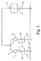
- Fig. 1 very schematically, is the circuit diagram of an inventive Proximity switch, namely a capacitive proximity switch, shown.
- This proximity switch initially includes two signal transmitters 1, 2 and a signal receiver 3.
- the two signal transmitters 1, 2 are on the one hand - each with their first signal output 4, 5 - with each other and with a first signal input 6 of the signal receiver 3 connected, on the other hand - each with its second Signal output 7, 8 - via one signal transmission path 9, 10 with the second Signal input 11 of the signal receiver 3 connected or connectable.
- At least is one of the two signal transmission paths 9 or 10 - by one, not shown Actuating object - can be influenced.
- the two Signal transmitter 1, 2 generate frequency spread signals. This is shown in the Embodiments of two signal transmitters 1, 2 a noise signal source 12 assigned. To what is achieved in that the two signal transmitters 1, 2 - in Connection to noise signal source 12 - generate frequency spread signals, is again based on the entire disclosure content of the German patent application 198 13 013.
- the reference capacity 2 is a special one as a capacitor in the exemplary embodiment according to FIG executed capacity 17 is provided as a reference capacity.
- a ground electrode 18 is provided for the transmission electrodes 13 and 14.
- the two signal transmitters 1, 2 Generate signals that are 180 ° out of phase - because that's the consequence has that when an actuating object the two signal transmission paths 9, 10th influenced identically, the only signal receiver 3 is supplied with a zero signal, so that any deviation from that with identical influence on the signal transmission paths 9, 10 occurring zero signal is particularly well recognized or processed can be. Consequently, it is provided for all illustrated embodiments that the two signal transmitters 1, 2 generate signals that are 180 ° out of phase.
- this is achieved in that the two Signal transmitter 1, 2 from a signal transmitter 1, 2 common signal generator 19 and in each case a switch located in series with the signal generator 19 20, 21 exist and that one of the two switches 20, 21, in the in Fig. 2nd and 3 illustrated embodiments, the switch 21, an inverter 22 upstream or downstream is connected downstream.
- capacitive proximity switch applies that the signal receiver 3 one the second Signal input 11 downstream phase sensitive synchronous rectifier 23, which in turn has a switch 24 on the input side.
- the two in series to the signal generator 19 lying switch 20, 21 and the switch 24 of the synchronous rectifier 23 are controlled simultaneously switching, in the in Figs.
- capacitive proximity switch For the embodiments shown in FIGS. 2 and 3 according to the invention capacitive proximity switch the following is also important:
- the signal receiver 3 is - with his first signal input 6, which is shown three times, and with its second signal input 11 - between the earth potential and the earth potential 28.
- the ground potential 28 as a - fixed - reference potential, so the Signal inputs 6 and 11 of the signal receiver 3 a signal only become effective or are present when "floating" of the ground potential 29 is possible is.
- the exemplary embodiments shown are more inventive capacitive proximity switch with two connection of the proximity switch provided with operating voltage connections 30, 31 serving an operating voltage, wherein the operating voltage connection 31 is at the ground potential 28.
- the ground potential 29 can "float" with respect to the ground potential 28, that is Ground potential 29, the DC or DC voltage with the earth potential 28 is connected, radio frequency decoupled from the ground potential 28, and This is because the operating voltage connections 30, 31 each have a - preferably current compensated - choke 32, 33 is connected downstream.
- the throttle is there 33 parallel to the signal inputs 6, 11 of the signal receiver 3, which, because of the low impedance for an alternating voltage at 50 Hz, a so-called mains hum is suppressed.
- Embodiments of capacitive proximity switches according to the invention still further Functional elements are provided, namely a voltage regulator 34 on the input side, between the operating voltage connection 30 and the choke 32 Blocking capacitor 35 connected to the operating voltage connections 30, 31 distal ends of the chokes 32, 33, a coupling capacitor 36 before second signal input 11 of signal receiver 3 and one of signal receiver 3 downstream amplifier 37, which can be provided with a protective circuit.
- the second transmitter electrode 14 concentrically surrounds the first Transmitting electrode 13.
- the capacitive proximity switch designed in this way is laterally insensitive, because the second transmission electrode 14 against the first transmission electrode 13 works.
- the two transmitting electrodes 13, 14 arranged side by side, namely opposite a counter electrode 38, which is connected to the ground potential 28.
- This embodiment enables e.g. B. counting labels, recognizing glue points and comparing of material thicknesses.
- a signal delay element namely a resistor 39, 40
- Another resistor 41 is in front of the second signal input 11 of the signal receiver 3 intended.
- the resistors 39, 40, 41 cause the signal currents to be somewhat flow with a time delay so that the synchronous rectifier 23 when the signal currents "arrive", is already “ready to receive", - although that to the synchronous rectifier 23 belonging switch 24 simultaneously with the two switches 20, 21, which belong to the signal transmitters 1, 2, switches.
- Fig. 3 is for controlling the two signal transmitters 1, 2 or the output signals of the signal transmitter 1, 2 the output signal of the analog amplifier 27 used.
- FIG. 3 That which was previously essentially functional, nevertheless for the person skilled in the art without further ado reworkable, has been explained, is still in the embodiment of FIG. 3 presented a little more specifically.
- This embodiment is complementary characterized in that the control of the output signals of the Signal transmitter 1, 2 the output of the analog amplifier 27 is a DC-controlled linear amplitude modulator or RF generator, preferably in the form of a CMOS analog switch 42, is connected downstream.
- CMOS analog switch 42 has the particular advantage of linearity, i.e. H. the DC voltage signal supplied to it is transformed 1: 1 into an AC signal.
- both signal transmitters 1, 2 and the output signals of both signal transmitters 1, 2 are controlled or are regulated. But there is also the option of only signal transmitter 1 or only to control or regulate the signal transmitter 2.
- the signal transmitter 1 as the measuring transmitter and the signal transmitter 2 as the reference transmitter
- the output signal of the Signal transmitter 1 as a measurement signal
- the output signal of the signal transmitter 2 as Reference signal
- the output signal of signal transmitter 1 i.e. the measurement signal
- the output signal of signal transmitter 2 is controlled or regulated
- the reference signal to control or regulate is particularly useful if both signal transmission paths can be influenced operationally, such as that has been explained above.
Applications Claiming Priority (2)
| Application Number | Priority Date | Filing Date | Title |
|---|---|---|---|
| DE19949998 | 1999-10-15 | ||
| DE19949998 | 1999-10-15 |
Publications (3)
| Publication Number | Publication Date |
|---|---|
| EP1093225A2 true EP1093225A2 (fr) | 2001-04-18 |
| EP1093225A3 EP1093225A3 (fr) | 2001-09-12 |
| EP1093225B1 EP1093225B1 (fr) | 2005-06-08 |
Family
ID=7925941
Family Applications (1)
| Application Number | Title | Priority Date | Filing Date |
|---|---|---|---|
| EP00122541A Expired - Lifetime EP1093225B1 (fr) | 1999-10-15 | 2000-10-16 | Commutateur de proximité |
Country Status (4)
| Country | Link |
|---|---|
| US (1) | US6664661B1 (fr) |
| EP (1) | EP1093225B1 (fr) |
| AT (1) | ATE297606T1 (fr) |
| DE (2) | DE10051292A1 (fr) |
Cited By (7)
| Publication number | Priority date | Publication date | Assignee | Title |
|---|---|---|---|---|
| WO2010115940A1 (fr) | 2009-04-07 | 2010-10-14 | Ident Technology Ag | Dispositif capteur et procédé de détection de réseau électrique et de proximité |
| WO2011138084A1 (fr) * | 2010-05-07 | 2011-11-10 | Robert Bosch Gmbh | Appareil de recherche |
| WO2012031965A1 (fr) * | 2010-09-09 | 2012-03-15 | Ident Technology Ag | Dispositif à capteur et procédé de détection de proximité et de toucher |
| CN102498669A (zh) * | 2009-04-07 | 2012-06-13 | 艾登特科技股份公司 | 用于抓握和靠近检测的传感器设备和方法 |
| US8587329B2 (en) | 2009-04-14 | 2013-11-19 | Balluff Gmbh | Circuit arrangement for determination of a measuring capacitance |
| DE102009061064B4 (de) * | 2009-07-08 | 2013-11-28 | Ident Technology Ag | Detektionseinrichtung für ein elektrisches Handgerät sowie Handgerät mit einer Detektionseinrichtung |
| DE102009057960B4 (de) * | 2009-12-11 | 2014-02-20 | Ident Technology Ag | Sensoreinrichtung und Verfahren zur Detektion eines Umgreifens eines Handgerätes mit zumindest einer Hand |
Families Citing this family (10)
| Publication number | Priority date | Publication date | Assignee | Title |
|---|---|---|---|---|
| DE10205445B4 (de) | 2002-02-08 | 2007-03-01 | Ifm Electronic Gmbh | Kapazitives Füllstandmeßgerät |
| DE102009016355B3 (de) * | 2009-04-07 | 2010-07-08 | Ident Technology Ag | Messelektrodenanordnung zur verbesserten Näherungsdetektion |
| US8493074B2 (en) | 2008-04-25 | 2013-07-23 | Ident Technology Ag | Electrode system for proximity detection and hand-held device with electrode system |
| DE102010019841A1 (de) | 2010-05-07 | 2011-11-10 | Ident Technology Ag | Leiterplatte für Display und Anzeigemodul mit Display und Leiterplatte |
| DE102011002447B4 (de) * | 2011-01-04 | 2014-07-10 | Ident Technology Ag | Kapazitiver Annäherungsensor sowie Verfahren zur kapazitiven Annäherungsdetektion |
| DE102011002603B4 (de) * | 2011-01-12 | 2013-10-31 | Ident Technology Ag | Kapazitive Sensoreinrichtung sowie Verfahren zum Betreiben einer kapazitiven Sensoreinrichtung |
| DE102013102237B4 (de) * | 2013-03-06 | 2015-03-19 | K.A. Schmersal Holding Gmbh & Co. Kg | Kapazitiver Positionsschalter |
| DE102013014824A1 (de) * | 2013-09-10 | 2015-03-12 | Brose Fahrzeugteile Gmbh & Co. Kommanditgesellschaft, Hallstadt | Kapazitiver Sensor für ein Fahrzeug |
| GB2541740B (en) * | 2015-08-28 | 2017-12-06 | Novalia Ltd | Capacitive touch-enabled article |
| EP3512098A1 (fr) * | 2018-01-10 | 2019-07-17 | Captron Electronic GmbH | Commutateur de capteur avec signal de détection de spectre étalé et redresseur synchrone |
Citations (7)
| Publication number | Priority date | Publication date | Assignee | Title |
|---|---|---|---|---|
| CH584981A5 (en) * | 1975-05-23 | 1977-02-15 | Baumgartner M Ag | Proximity switch with two capacitative sensor plates - is activated by imbalance in outputs of two HF oscillators coupled to comparator |
| US4972154A (en) * | 1989-06-06 | 1990-11-20 | Metriguard, Inc | Apparatus and method for measuring wood grain angle |
| EP0438634A2 (fr) * | 1990-01-23 | 1991-07-31 | VDO Adolf Schindling AG | Circuit d'évaluation pour capteur capacitif |
| DE4004530A1 (de) * | 1990-02-14 | 1991-08-22 | Stefan Reich | Optische abstandsmessung |
| DE19701899A1 (de) * | 1996-01-21 | 1997-10-30 | Ifm Electronic Gmbh | Schaltungsanordnung zur Erfassung der Kapazität bzw. einer Kapazitätsänderung eines kapazitiven Schaltungs- oder Bauelementes |
| EP0908736A2 (fr) * | 1997-10-07 | 1999-04-14 | i f m electronic gmbh | Circuit pour déterminer la capacité ou la variation de capacité d'un circuit ou module capacitif |
| EP0945984A2 (fr) * | 1998-03-25 | 1999-09-29 | i f m electronic gmbh | Procédé d'opération d'un commutateur capacitif et circuit de commutation capacitif |
Family Cites Families (9)
| Publication number | Priority date | Publication date | Assignee | Title |
|---|---|---|---|---|
| DE2460057B2 (de) * | 1974-12-19 | 1977-02-10 | Robert Bosch Gmbh, 7000 Stuttgart | Schaltanordnung mit einem streufeldkondensator |
| JPS5363582A (en) * | 1976-11-18 | 1978-06-07 | Mitsubishi Electric Corp | Proximity detector |
| JPS606280B2 (ja) * | 1977-03-24 | 1985-02-16 | 三菱電機株式会社 | 近接検出装置 |
| DE2719955C2 (de) * | 1977-05-04 | 1982-12-02 | M.A.N. Maschinenfabrik Augsburg-Nürnberg AG, 8500 Nürnberg | Feldsensor zum Erkennen von Personen oder Gegenständen, insbesondere vor Aufzug-Schiebetüren |
| US4316180A (en) * | 1979-04-09 | 1982-02-16 | Levert Francis E | Directional detector of changes in a local electrostatic field |
| US4349814A (en) * | 1979-10-08 | 1982-09-14 | Duraplug Electricals Limited | Electric switches |
| DE3327329A1 (de) * | 1983-07-29 | 1985-02-14 | Robert Ing.(grad.) 7995 Neukirch Buck | Elektronisches, vorzugsweise beruehrungslos arbeitendes schaltgeraet |
| GB2279750A (en) * | 1993-07-10 | 1995-01-11 | Paul Thomas Ryan | Capacitive proximity sensor |
| DE19812626A1 (de) | 1998-03-23 | 1999-09-30 | Bayerische Motoren Werke Ag | Verfahren zur kapazitiven Objekterkennung bei Fahrzeugen |
-
2000
- 2000-10-16 DE DE10051292A patent/DE10051292A1/de not_active Withdrawn
- 2000-10-16 EP EP00122541A patent/EP1093225B1/fr not_active Expired - Lifetime
- 2000-10-16 DE DE50010501T patent/DE50010501D1/de not_active Expired - Lifetime
- 2000-10-16 AT AT00122541T patent/ATE297606T1/de active
- 2000-10-16 US US09/688,744 patent/US6664661B1/en not_active Expired - Lifetime
Patent Citations (7)
| Publication number | Priority date | Publication date | Assignee | Title |
|---|---|---|---|---|
| CH584981A5 (en) * | 1975-05-23 | 1977-02-15 | Baumgartner M Ag | Proximity switch with two capacitative sensor plates - is activated by imbalance in outputs of two HF oscillators coupled to comparator |
| US4972154A (en) * | 1989-06-06 | 1990-11-20 | Metriguard, Inc | Apparatus and method for measuring wood grain angle |
| EP0438634A2 (fr) * | 1990-01-23 | 1991-07-31 | VDO Adolf Schindling AG | Circuit d'évaluation pour capteur capacitif |
| DE4004530A1 (de) * | 1990-02-14 | 1991-08-22 | Stefan Reich | Optische abstandsmessung |
| DE19701899A1 (de) * | 1996-01-21 | 1997-10-30 | Ifm Electronic Gmbh | Schaltungsanordnung zur Erfassung der Kapazität bzw. einer Kapazitätsänderung eines kapazitiven Schaltungs- oder Bauelementes |
| EP0908736A2 (fr) * | 1997-10-07 | 1999-04-14 | i f m electronic gmbh | Circuit pour déterminer la capacité ou la variation de capacité d'un circuit ou module capacitif |
| EP0945984A2 (fr) * | 1998-03-25 | 1999-09-29 | i f m electronic gmbh | Procédé d'opération d'un commutateur capacitif et circuit de commutation capacitif |
Cited By (10)
| Publication number | Priority date | Publication date | Assignee | Title |
|---|---|---|---|---|
| WO2010115940A1 (fr) | 2009-04-07 | 2010-10-14 | Ident Technology Ag | Dispositif capteur et procédé de détection de réseau électrique et de proximité |
| CN102498669A (zh) * | 2009-04-07 | 2012-06-13 | 艾登特科技股份公司 | 用于抓握和靠近检测的传感器设备和方法 |
| US9236860B2 (en) | 2009-04-07 | 2016-01-12 | Microchip Technology Germany Gmbh | Sensor device and method for grip and proximity detection |
| US8587329B2 (en) | 2009-04-14 | 2013-11-19 | Balluff Gmbh | Circuit arrangement for determination of a measuring capacitance |
| DE102009061064B4 (de) * | 2009-07-08 | 2013-11-28 | Ident Technology Ag | Detektionseinrichtung für ein elektrisches Handgerät sowie Handgerät mit einer Detektionseinrichtung |
| DE102009057960B4 (de) * | 2009-12-11 | 2014-02-20 | Ident Technology Ag | Sensoreinrichtung und Verfahren zur Detektion eines Umgreifens eines Handgerätes mit zumindest einer Hand |
| WO2011138084A1 (fr) * | 2010-05-07 | 2011-11-10 | Robert Bosch Gmbh | Appareil de recherche |
| CN102859873A (zh) * | 2010-05-07 | 2013-01-02 | 罗伯特·博世有限公司 | 搜索设备 |
| CN102859873B (zh) * | 2010-05-07 | 2016-01-13 | 罗伯特·博世有限公司 | 搜索设备 |
| WO2012031965A1 (fr) * | 2010-09-09 | 2012-03-15 | Ident Technology Ag | Dispositif à capteur et procédé de détection de proximité et de toucher |
Also Published As
| Publication number | Publication date |
|---|---|
| DE10051292A1 (de) | 2001-05-10 |
| DE50010501D1 (de) | 2005-07-14 |
| ATE297606T1 (de) | 2005-06-15 |
| EP1093225A3 (fr) | 2001-09-12 |
| US6664661B1 (en) | 2003-12-16 |
| EP1093225B1 (fr) | 2005-06-08 |
Similar Documents
| Publication | Publication Date | Title |
|---|---|---|
| EP1093225B1 (fr) | Commutateur de proximité | |
| DE4007385A1 (de) | Schaltungsanordnung zum automatischen nullpunkt-abgleich zur behebung von offsetfehlern | |
| DE3238254C2 (fr) | ||
| DE102004034190A1 (de) | Oszillatorschaltung | |
| DE10050294B4 (de) | PLL-Schaltung | |
| DE3522994C2 (fr) | ||
| EP0025029B1 (fr) | Dispositif de pont de mesure capacitif | |
| EP1490655B1 (fr) | Circuit servant a redresser la tension de sortie d'un capteur alimente par un oscillateur | |
| DE4203725C2 (de) | Anordnung zur potentialgetrennten Kapazitätsmessung, insbesondere zur kapazitiven Füllstandmessung | |
| EP0743750B1 (fr) | Dispositif électronique de commutation, de préférence avec opération sans contact | |
| DE3024014C2 (de) | Wechsel-Gleichspannungswandler in Form einer integrierten Schaltung | |
| DE1541874A1 (de) | Daempfungs-Schaltung | |
| DE2826536B1 (de) | Schaltungsanordnung zur erdfreien UEbertragung von Signalen ueber Trennstellen in Fernmeldeanlagen | |
| EP3141878A2 (fr) | Dispositif et procédé de fonctionnement de capteurs à infrarouge passif | |
| DE3026551C2 (fr) | ||
| DE2212564C3 (de) | Elektronische Schalteranordnung für Videosignale | |
| DE954431C (de) | Anordnung zur Bandbreitenvergroesserung von Transistorschaltungen | |
| DE2743099A1 (de) | Schaltungsanordnung mit transistoren | |
| DE3408529C2 (fr) | ||
| DE2917020A1 (de) | Linearer verstaerker | |
| WO2001014895A1 (fr) | Circuit et procede d'evaluation de capacites | |
| WO2021069071A1 (fr) | Circuit électrique | |
| DE10304873B4 (de) | Schaltungsanordnung mit einem Wanderwellenverstärker | |
| DE3737862C2 (fr) | ||
| DE933942C (de) | Anordnung zum Erzeugen linearisierter saegezahnfoermiger Stroeme |
Legal Events
| Date | Code | Title | Description |
|---|---|---|---|
| PUAI | Public reference made under article 153(3) epc to a published international application that has entered the european phase |
Free format text: ORIGINAL CODE: 0009012 |
|
| AK | Designated contracting states |
Kind code of ref document: A2 Designated state(s): AT BE CH CY DE DK ES FI FR GB GR IE IT LI LU MC NL PT SE |
|
| AX | Request for extension of the european patent |
Free format text: AL;LT;LV;MK;RO;SI |
|
| PUAL | Search report despatched |
Free format text: ORIGINAL CODE: 0009013 |
|
| AK | Designated contracting states |
Kind code of ref document: A3 Designated state(s): AT BE CH CY DE DK ES FI FR GB GR IE IT LI LU MC NL PT SE |
|
| AX | Request for extension of the european patent |
Free format text: AL;LT;LV;MK;RO;SI |
|
| 17P | Request for examination filed |
Effective date: 20011220 |
|
| AKX | Designation fees paid |
Free format text: AT BE CH CY DE DK ES FI FR GB GR IE IT LI LU MC NL PT SE |
|
| 17Q | First examination report despatched |
Effective date: 20030904 |
|
| GRAP | Despatch of communication of intention to grant a patent |
Free format text: ORIGINAL CODE: EPIDOSNIGR1 |
|
| GRAS | Grant fee paid |
Free format text: ORIGINAL CODE: EPIDOSNIGR3 |
|
| GRAA | (expected) grant |
Free format text: ORIGINAL CODE: 0009210 |
|
| AK | Designated contracting states |
Kind code of ref document: B1 Designated state(s): AT BE CH CY DE DK ES FI FR GB GR IE IT LI LU MC NL PT SE |
|
| PG25 | Lapsed in a contracting state [announced via postgrant information from national office to epo] |
Ref country code: IE Free format text: LAPSE BECAUSE OF FAILURE TO SUBMIT A TRANSLATION OF THE DESCRIPTION OR TO PAY THE FEE WITHIN THE PRESCRIBED TIME-LIMIT Effective date: 20050608 Ref country code: FI Free format text: LAPSE BECAUSE OF FAILURE TO SUBMIT A TRANSLATION OF THE DESCRIPTION OR TO PAY THE FEE WITHIN THE PRESCRIBED TIME-LIMIT Effective date: 20050608 Ref country code: IT Free format text: LAPSE BECAUSE OF FAILURE TO SUBMIT A TRANSLATION OF THE DESCRIPTION OR TO PAY THE FEE WITHIN THE PRESCRIBED TIME-LIMIT;WARNING: LAPSES OF ITALIAN PATENTS WITH EFFECTIVE DATE BEFORE 2007 MAY HAVE OCCURRED AT ANY TIME BEFORE 2007. THE CORRECT EFFECTIVE DATE MAY BE DIFFERENT FROM THE ONE RECORDED. Effective date: 20050608 |
|
| REG | Reference to a national code |
Ref country code: GB Ref legal event code: FG4D Free format text: NOT ENGLISH |
|
| REG | Reference to a national code |
Ref country code: CH Ref legal event code: EP |
|
| REF | Corresponds to: |
Ref document number: 50010501 Country of ref document: DE Date of ref document: 20050714 Kind code of ref document: P |
|
| REG | Reference to a national code |
Ref country code: IE Ref legal event code: FG4D Free format text: LANGUAGE OF EP DOCUMENT: GERMAN |
|
| PG25 | Lapsed in a contracting state [announced via postgrant information from national office to epo] |
Ref country code: GR Free format text: LAPSE BECAUSE OF FAILURE TO SUBMIT A TRANSLATION OF THE DESCRIPTION OR TO PAY THE FEE WITHIN THE PRESCRIBED TIME-LIMIT Effective date: 20050908 Ref country code: DK Free format text: LAPSE BECAUSE OF FAILURE TO SUBMIT A TRANSLATION OF THE DESCRIPTION OR TO PAY THE FEE WITHIN THE PRESCRIBED TIME-LIMIT Effective date: 20050908 Ref country code: SE Free format text: LAPSE BECAUSE OF FAILURE TO SUBMIT A TRANSLATION OF THE DESCRIPTION OR TO PAY THE FEE WITHIN THE PRESCRIBED TIME-LIMIT Effective date: 20050908 |
|
| GBT | Gb: translation of ep patent filed (gb section 77(6)(a)/1977) |
Effective date: 20050822 |
|
| PG25 | Lapsed in a contracting state [announced via postgrant information from national office to epo] |
Ref country code: ES Free format text: LAPSE BECAUSE OF FAILURE TO SUBMIT A TRANSLATION OF THE DESCRIPTION OR TO PAY THE FEE WITHIN THE PRESCRIBED TIME-LIMIT Effective date: 20050919 |
|
| PG25 | Lapsed in a contracting state [announced via postgrant information from national office to epo] |
Ref country code: CY Free format text: LAPSE BECAUSE OF FAILURE TO SUBMIT A TRANSLATION OF THE DESCRIPTION OR TO PAY THE FEE WITHIN THE PRESCRIBED TIME-LIMIT Effective date: 20051016 |
|
| PG25 | Lapsed in a contracting state [announced via postgrant information from national office to epo] |
Ref country code: MC Free format text: LAPSE BECAUSE OF NON-PAYMENT OF DUE FEES Effective date: 20051031 Ref country code: BE Free format text: LAPSE BECAUSE OF NON-PAYMENT OF DUE FEES Effective date: 20051031 Ref country code: CH Free format text: LAPSE BECAUSE OF NON-PAYMENT OF DUE FEES Effective date: 20051031 Ref country code: LI Free format text: LAPSE BECAUSE OF NON-PAYMENT OF DUE FEES Effective date: 20051031 Ref country code: LU Free format text: LAPSE BECAUSE OF NON-PAYMENT OF DUE FEES Effective date: 20051031 |
|
| PG25 | Lapsed in a contracting state [announced via postgrant information from national office to epo] |
Ref country code: PT Free format text: LAPSE BECAUSE OF FAILURE TO SUBMIT A TRANSLATION OF THE DESCRIPTION OR TO PAY THE FEE WITHIN THE PRESCRIBED TIME-LIMIT Effective date: 20051114 |
|
| REG | Reference to a national code |
Ref country code: IE Ref legal event code: FD4D |
|
| ET | Fr: translation filed | ||
| PLBE | No opposition filed within time limit |
Free format text: ORIGINAL CODE: 0009261 |
|
| STAA | Information on the status of an ep patent application or granted ep patent |
Free format text: STATUS: NO OPPOSITION FILED WITHIN TIME LIMIT |
|
| 26N | No opposition filed |
Effective date: 20060309 |
|
| REG | Reference to a national code |
Ref country code: CH Ref legal event code: PL |
|
| BERE | Be: lapsed |
Owner name: I F M ELECTRONIC G.M.B.H. Effective date: 20051031 |
|
| PGFP | Annual fee paid to national office [announced via postgrant information from national office to epo] |
Ref country code: FR Payment date: 20131018 Year of fee payment: 14 Ref country code: GB Payment date: 20131022 Year of fee payment: 14 Ref country code: AT Payment date: 20131021 Year of fee payment: 14 |
|
| PGFP | Annual fee paid to national office [announced via postgrant information from national office to epo] |
Ref country code: NL Payment date: 20131021 Year of fee payment: 14 |
|
| REG | Reference to a national code |
Ref country code: NL Ref legal event code: V1 Effective date: 20150501 |
|
| REG | Reference to a national code |
Ref country code: AT Ref legal event code: MM01 Ref document number: 297606 Country of ref document: AT Kind code of ref document: T Effective date: 20141016 |
|
| GBPC | Gb: european patent ceased through non-payment of renewal fee |
Effective date: 20141016 |
|
| PG25 | Lapsed in a contracting state [announced via postgrant information from national office to epo] |
Ref country code: GB Free format text: LAPSE BECAUSE OF NON-PAYMENT OF DUE FEES Effective date: 20141016 |
|
| REG | Reference to a national code |
Ref country code: FR Ref legal event code: ST Effective date: 20150630 |
|
| PG25 | Lapsed in a contracting state [announced via postgrant information from national office to epo] |
Ref country code: AT Free format text: LAPSE BECAUSE OF NON-PAYMENT OF DUE FEES Effective date: 20141016 Ref country code: FR Free format text: LAPSE BECAUSE OF NON-PAYMENT OF DUE FEES Effective date: 20141031 Ref country code: NL Free format text: LAPSE BECAUSE OF NON-PAYMENT OF DUE FEES Effective date: 20150501 |
|
| PGFP | Annual fee paid to national office [announced via postgrant information from national office to epo] |
Ref country code: DE Payment date: 20181024 Year of fee payment: 19 |
|
| REG | Reference to a national code |
Ref country code: DE Ref legal event code: R119 Ref document number: 50010501 Country of ref document: DE |
|
| PG25 | Lapsed in a contracting state [announced via postgrant information from national office to epo] |
Ref country code: DE Free format text: LAPSE BECAUSE OF NON-PAYMENT OF DUE FEES Effective date: 20200501 |