EP1083596B1 - A method to create a copper dual damascene structure with less dishing and erosion - Google Patents
A method to create a copper dual damascene structure with less dishing and erosion Download PDFInfo
- Publication number
- EP1083596B1 EP1083596B1 EP00640007A EP00640007A EP1083596B1 EP 1083596 B1 EP1083596 B1 EP 1083596B1 EP 00640007 A EP00640007 A EP 00640007A EP 00640007 A EP00640007 A EP 00640007A EP 1083596 B1 EP1083596 B1 EP 1083596B1
- Authority
- EP
- European Patent Office
- Prior art keywords
- layer
- dielectric
- copper
- depositing
- dual damascene
- Prior art date
- Legal status (The legal status is an assumption and is not a legal conclusion. Google has not performed a legal analysis and makes no representation as to the accuracy of the status listed.)
- Expired - Lifetime
Links
Images

Classifications
-
- H—ELECTRICITY
- H01—ELECTRIC ELEMENTS
- H01L—SEMICONDUCTOR DEVICES NOT COVERED BY CLASS H10
- H01L21/00—Processes or apparatus adapted for the manufacture or treatment of semiconductor or solid state devices or of parts thereof
- H01L21/70—Manufacture or treatment of devices consisting of a plurality of solid state components formed in or on a common substrate or of parts thereof; Manufacture of integrated circuit devices or of parts thereof
- H01L21/71—Manufacture of specific parts of devices defined in group H01L21/70
- H01L21/768—Applying interconnections to be used for carrying current between separate components within a device comprising conductors and dielectrics
- H01L21/76801—Applying interconnections to be used for carrying current between separate components within a device comprising conductors and dielectrics characterised by the formation and the after-treatment of the dielectrics, e.g. smoothing
- H01L21/76829—Applying interconnections to be used for carrying current between separate components within a device comprising conductors and dielectrics characterised by the formation and the after-treatment of the dielectrics, e.g. smoothing characterised by the formation of thin functional dielectric layers, e.g. dielectric etch-stop, barrier, capping or liner layers
- H01L21/76834—Applying interconnections to be used for carrying current between separate components within a device comprising conductors and dielectrics characterised by the formation and the after-treatment of the dielectrics, e.g. smoothing characterised by the formation of thin functional dielectric layers, e.g. dielectric etch-stop, barrier, capping or liner layers formation of thin insulating films on the sidewalls or on top of conductors
-
- H—ELECTRICITY
- H01—ELECTRIC ELEMENTS
- H01L—SEMICONDUCTOR DEVICES NOT COVERED BY CLASS H10
- H01L21/00—Processes or apparatus adapted for the manufacture or treatment of semiconductor or solid state devices or of parts thereof
- H01L21/02—Manufacture or treatment of semiconductor devices or of parts thereof
- H01L21/04—Manufacture or treatment of semiconductor devices or of parts thereof the devices having potential barriers, e.g. a PN junction, depletion layer or carrier concentration layer
- H01L21/18—Manufacture or treatment of semiconductor devices or of parts thereof the devices having potential barriers, e.g. a PN junction, depletion layer or carrier concentration layer the devices having semiconductor bodies comprising elements of Group IV of the Periodic Table or AIIIBV compounds with or without impurities, e.g. doping materials
- H01L21/30—Treatment of semiconductor bodies using processes or apparatus not provided for in groups H01L21/20 - H01L21/26
- H01L21/31—Treatment of semiconductor bodies using processes or apparatus not provided for in groups H01L21/20 - H01L21/26 to form insulating layers thereon, e.g. for masking or by using photolithographic techniques; After treatment of these layers; Selection of materials for these layers
- H01L21/3205—Deposition of non-insulating-, e.g. conductive- or resistive-, layers on insulating layers; After-treatment of these layers
- H01L21/321—After treatment
- H01L21/32115—Planarisation
- H01L21/3212—Planarisation by chemical mechanical polishing [CMP]
-
- H—ELECTRICITY
- H01—ELECTRIC ELEMENTS
- H01L—SEMICONDUCTOR DEVICES NOT COVERED BY CLASS H10
- H01L21/00—Processes or apparatus adapted for the manufacture or treatment of semiconductor or solid state devices or of parts thereof
- H01L21/70—Manufacture or treatment of devices consisting of a plurality of solid state components formed in or on a common substrate or of parts thereof; Manufacture of integrated circuit devices or of parts thereof
- H01L21/71—Manufacture of specific parts of devices defined in group H01L21/70
- H01L21/768—Applying interconnections to be used for carrying current between separate components within a device comprising conductors and dielectrics
- H01L21/76801—Applying interconnections to be used for carrying current between separate components within a device comprising conductors and dielectrics characterised by the formation and the after-treatment of the dielectrics, e.g. smoothing
- H01L21/76802—Applying interconnections to be used for carrying current between separate components within a device comprising conductors and dielectrics characterised by the formation and the after-treatment of the dielectrics, e.g. smoothing by forming openings in dielectrics
- H01L21/76807—Applying interconnections to be used for carrying current between separate components within a device comprising conductors and dielectrics characterised by the formation and the after-treatment of the dielectrics, e.g. smoothing by forming openings in dielectrics for dual damascene structures
-
- H—ELECTRICITY
- H01—ELECTRIC ELEMENTS
- H01L—SEMICONDUCTOR DEVICES NOT COVERED BY CLASS H10
- H01L21/00—Processes or apparatus adapted for the manufacture or treatment of semiconductor or solid state devices or of parts thereof
- H01L21/70—Manufacture or treatment of devices consisting of a plurality of solid state components formed in or on a common substrate or of parts thereof; Manufacture of integrated circuit devices or of parts thereof
- H01L21/71—Manufacture of specific parts of devices defined in group H01L21/70
- H01L21/768—Applying interconnections to be used for carrying current between separate components within a device comprising conductors and dielectrics
- H01L21/76838—Applying interconnections to be used for carrying current between separate components within a device comprising conductors and dielectrics characterised by the formation and the after-treatment of the conductors
- H01L21/7684—Smoothing; Planarisation
-
- H—ELECTRICITY
- H01—ELECTRIC ELEMENTS
- H01L—SEMICONDUCTOR DEVICES NOT COVERED BY CLASS H10
- H01L23/00—Details of semiconductor or other solid state devices
- H01L23/52—Arrangements for conducting electric current within the device in operation from one component to another, i.e. interconnections, e.g. wires, lead frames
- H01L23/522—Arrangements for conducting electric current within the device in operation from one component to another, i.e. interconnections, e.g. wires, lead frames including external interconnections consisting of a multilayer structure of conductive and insulating layers inseparably formed on the semiconductor body
- H01L23/532—Arrangements for conducting electric current within the device in operation from one component to another, i.e. interconnections, e.g. wires, lead frames including external interconnections consisting of a multilayer structure of conductive and insulating layers inseparably formed on the semiconductor body characterised by the materials
- H01L23/53204—Conductive materials
- H01L23/53209—Conductive materials based on metals, e.g. alloys, metal silicides
- H01L23/53228—Conductive materials based on metals, e.g. alloys, metal silicides the principal metal being copper
- H01L23/53238—Additional layers associated with copper layers, e.g. adhesion, barrier, cladding layers
-
- H—ELECTRICITY
- H01—ELECTRIC ELEMENTS
- H01L—SEMICONDUCTOR DEVICES NOT COVERED BY CLASS H10
- H01L2924/00—Indexing scheme for arrangements or methods for connecting or disconnecting semiconductor or solid-state bodies as covered by H01L24/00
- H01L2924/0001—Technical content checked by a classifier
- H01L2924/0002—Not covered by any one of groups H01L24/00, H01L24/00 and H01L2224/00
Definitions
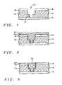
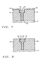
- the invention relates to the fabrication of integrated circuit devices, and more particularly, to a method of reducing dishing and erosion of the copper surface during and after copper Chemical Mechanical Planarization (CMP).
- CMP Chemical Mechanical Planarization
Landscapes
- Engineering & Computer Science (AREA)
- Physics & Mathematics (AREA)
- Condensed Matter Physics & Semiconductors (AREA)
- General Physics & Mathematics (AREA)
- Computer Hardware Design (AREA)
- Microelectronics & Electronic Packaging (AREA)
- Power Engineering (AREA)
- Manufacturing & Machinery (AREA)
- Internal Circuitry In Semiconductor Integrated Circuit Devices (AREA)
- Mechanical Treatment Of Semiconductor (AREA)
Applications Claiming Priority (2)
| Application Number | Priority Date | Filing Date | Title |
|---|---|---|---|
| US390783 | 1999-09-07 | ||
| US09/390,783 US6251786B1 (en) | 1999-09-07 | 1999-09-07 | Method to create a copper dual damascene structure with less dishing and erosion |
Publications (2)
| Publication Number | Publication Date |
|---|---|
| EP1083596A1 EP1083596A1 (en) | 2001-03-14 |
| EP1083596B1 true EP1083596B1 (en) | 2012-08-22 |
Family
ID=23543923
Family Applications (1)
| Application Number | Title | Priority Date | Filing Date |
|---|---|---|---|
| EP00640007A Expired - Lifetime EP1083596B1 (en) | 1999-09-07 | 2000-07-18 | A method to create a copper dual damascene structure with less dishing and erosion |
Country Status (4)
| Country | Link |
|---|---|
| US (1) | US6251786B1 (enExample) |
| EP (1) | EP1083596B1 (enExample) |
| JP (1) | JP4266502B2 (enExample) |
| SG (1) | SG121686A1 (enExample) |
Families Citing this family (43)
| Publication number | Priority date | Publication date | Assignee | Title |
|---|---|---|---|---|
| US6455425B1 (en) * | 2000-01-18 | 2002-09-24 | Advanced Micro Devices, Inc. | Selective deposition process for passivating top interface of damascene-type Cu interconnect lines |
| CN1358329A (zh) * | 2000-01-20 | 2002-07-10 | 皇家菲利浦电子有限公司 | 镶嵌结构及其制作方法 |
| US6368953B1 (en) | 2000-05-09 | 2002-04-09 | International Business Machines Corporation | Encapsulated metal structures for semiconductor devices and MIM capacitors including the same |
| KR100671610B1 (ko) | 2000-10-26 | 2007-01-18 | 주식회사 하이닉스반도체 | 반도체 소자의 금속 배선 형성 방법 |
| US6709874B2 (en) * | 2001-01-24 | 2004-03-23 | Infineon Technologies Ag | Method of manufacturing a metal cap layer for preventing damascene conductive lines from oxidation |
| US6586326B2 (en) * | 2001-03-13 | 2003-07-01 | Lsi Logic Corporation | Metal planarization system |
| JP4350337B2 (ja) * | 2001-04-27 | 2009-10-21 | 富士通マイクロエレクトロニクス株式会社 | 半導体装置 |
| KR100435784B1 (ko) * | 2001-12-21 | 2004-06-12 | 동부전자 주식회사 | 반도체 소자의 금속배선 형성 방법 |
| KR100444301B1 (ko) * | 2001-12-29 | 2004-08-16 | 주식회사 하이닉스반도체 | 질화막 cmp를 이용한 다마신 금속 게이트 형성 방법 |
| JP4088120B2 (ja) * | 2002-08-12 | 2008-05-21 | 株式会社ルネサステクノロジ | 半導体装置 |
| US6670274B1 (en) * | 2002-10-01 | 2003-12-30 | Taiwan Semiconductor Manufacturing Company | Method of forming a copper damascene structure comprising a recessed copper-oxide-free initial copper structure |
| US6940108B2 (en) * | 2002-12-05 | 2005-09-06 | Taiwan Semiconductor Manufacturing Co., Ltd. | Slot design for metal interconnects |
| US7825516B2 (en) * | 2002-12-11 | 2010-11-02 | International Business Machines Corporation | Formation of aligned capped metal lines and interconnections in multilevel semiconductor structures |
| US6975032B2 (en) * | 2002-12-16 | 2005-12-13 | International Business Machines Corporation | Copper recess process with application to selective capping and electroless plating |
| KR20040060563A (ko) * | 2002-12-30 | 2004-07-06 | 동부전자 주식회사 | 반도체 소자 제조방법 및 구조 |
| US7294241B2 (en) * | 2003-01-03 | 2007-11-13 | Chartered Semiconductor Manufacturing Ltd. | Method to form alpha phase Ta and its application to IC manufacturing |
| US20040185992A1 (en) * | 2003-03-18 | 2004-09-23 | Tisdale Lucien E. | Method and apparatus for making a packaging article and packaging article made by the method and apparatus |
| JP4638140B2 (ja) * | 2003-07-09 | 2011-02-23 | マグナチップセミコンダクター有限会社 | 半導体素子の銅配線形成方法 |
| US20050079703A1 (en) * | 2003-10-09 | 2005-04-14 | Applied Materials, Inc. | Method for planarizing an interconnect structure |
| US7183199B2 (en) * | 2003-12-01 | 2007-02-27 | Taiwan Semiconductor Manufacturing Co., Ltd. | Method of reducing the pattern effect in the CMP process |
| US20050139292A1 (en) * | 2003-12-31 | 2005-06-30 | Suresh Ramarajan | Method and apparatus for minimizing thickness-to-planarity and dishing in CMP |
| US20060113675A1 (en) * | 2004-12-01 | 2006-06-01 | Chung-Liang Chang | Barrier material and process for Cu interconnect |
| DE102005004384A1 (de) * | 2005-01-31 | 2006-08-10 | Advanced Micro Devices, Inc., Sunnyvale | Verfahren zur Herstellung einer definierten Vertiefung in einer Damaszener-Struktur unter Verwendung eines CMP Prozesses und eine Damaszener-Struktur |
| US20060205204A1 (en) * | 2005-03-14 | 2006-09-14 | Michael Beck | Method of making a semiconductor interconnect with a metal cap |
| US20070080455A1 (en) * | 2005-10-11 | 2007-04-12 | International Business Machines Corporation | Semiconductors and methods of making |
| KR100729126B1 (ko) * | 2005-11-15 | 2007-06-14 | 동부일렉트로닉스 주식회사 | 반도체 소자의 금속 배선 및 그 형성 방법 |
| US7432205B2 (en) * | 2005-12-15 | 2008-10-07 | United Microelectronics Corp. | Method for controlling polishing process |
| CN100477120C (zh) * | 2005-12-30 | 2009-04-08 | 联华电子股份有限公司 | 抛光工艺的控制方法 |
| US7863183B2 (en) * | 2006-01-18 | 2011-01-04 | International Business Machines Corporation | Method for fabricating last level copper-to-C4 connection with interfacial cap structure |
| US7619310B2 (en) * | 2006-11-03 | 2009-11-17 | Infineon Technologies Ag | Semiconductor interconnect and method of making same |
| US7893459B2 (en) | 2007-04-10 | 2011-02-22 | Taiwan Semiconductor Manufacturing Company, Ltd. | Seal ring structures with reduced moisture-induced reliability degradation |
| US20090039512A1 (en) * | 2007-08-08 | 2009-02-12 | International Business Machines Corporation | Electromigration resistant interconnect structure |
| US20090200668A1 (en) * | 2008-02-07 | 2009-08-13 | International Business Machines Corporation | Interconnect structure with high leakage resistance |
| CN102203935A (zh) * | 2008-10-27 | 2011-09-28 | Nxp股份有限公司 | 生物兼容电极 |
| US8629063B2 (en) | 2011-06-08 | 2014-01-14 | International Business Machines Corporation | Forming features on a substrate having varying feature densities |
| KR102085086B1 (ko) | 2013-10-29 | 2020-03-05 | 삼성전자주식회사 | 반도체 장치 및 그 제조방법 |
| US10211278B2 (en) * | 2017-07-11 | 2019-02-19 | Texas Instruments Incorporated | Device and method for a thin film resistor using a via retardation layer |
| US11018087B2 (en) * | 2018-04-25 | 2021-05-25 | International Business Machines Corporation | Metal interconnects |
| US11282788B2 (en) | 2019-07-25 | 2022-03-22 | International Business Machines Corporation | Interconnect and memory structures formed in the BEOL |
| US11195751B2 (en) | 2019-09-13 | 2021-12-07 | International Business Machines Corporation | Bilayer barrier for interconnect and memory structures formed in the BEOL |
| FR3113125B1 (fr) * | 2020-07-29 | 2022-07-29 | Lynred | Procede de realisation d’un micro-bolometre d’imagerie infrarouge et micro-bolometre associe |
| TW202225649A (zh) | 2020-07-29 | 2022-07-01 | 法商林銳股份有限公司 | 紅外線成像微測輻射熱計及相關形成方法 |
| US12484210B2 (en) | 2022-02-17 | 2025-11-25 | Fujian Jinhua Integrated Circuit Co., Ltd. | Semiconductor structure and method for forming the same |
Family Cites Families (16)
| Publication number | Priority date | Publication date | Assignee | Title |
|---|---|---|---|---|
| JP3297220B2 (ja) * | 1993-10-29 | 2002-07-02 | 株式会社東芝 | 半導体装置の製造方法および半導体装置 |
| KR0138305B1 (ko) * | 1994-11-30 | 1998-06-01 | 김광호 | 반도체소자 배선형성방법 |
| US5674787A (en) | 1996-01-16 | 1997-10-07 | Sematech, Inc. | Selective electroless copper deposited interconnect plugs for ULSI applications |
| US5744376A (en) | 1996-04-08 | 1998-04-28 | Chartered Semiconductor Manufacturing Pte, Ltd | Method of manufacturing copper interconnect with top barrier layer |
| US5741626A (en) | 1996-04-15 | 1998-04-21 | Motorola, Inc. | Method for forming a dielectric tantalum nitride layer as an anti-reflective coating (ARC) |
| US5814557A (en) | 1996-05-20 | 1998-09-29 | Motorola, Inc. | Method of forming an interconnect structure |
| US5723387A (en) | 1996-07-22 | 1998-03-03 | Industrial Technology Research Institute | Method and apparatus for forming very small scale Cu interconnect metallurgy on semiconductor substrates |
| US5818110A (en) | 1996-11-22 | 1998-10-06 | International Business Machines Corporation | Integrated circuit chip wiring structure with crossover capability and method of manufacturing the same |
| US6069068A (en) * | 1997-05-30 | 2000-05-30 | International Business Machines Corporation | Sub-quarter-micron copper interconnections with improved electromigration resistance and reduced defect sensitivity |
| US5893752A (en) * | 1997-12-22 | 1999-04-13 | Motorola, Inc. | Process for forming a semiconductor device |
| US5920790A (en) * | 1997-08-29 | 1999-07-06 | Motorola, Inc. | Method of forming a semiconductor device having dual inlaid structure |
| US6103625A (en) * | 1997-12-31 | 2000-08-15 | Intel Corporation | Use of a polish stop layer in the formation of metal structures |
| US6017803A (en) * | 1998-06-24 | 2000-01-25 | Chartered Semiconductor Manufacturing, Ltd. | Method to prevent dishing in chemical mechanical polishing |
| US6083835A (en) * | 1998-07-24 | 2000-07-04 | Taiwan Semiconductor Manufacturing Company | Self-passivation of copper damascene |
| US6114246A (en) * | 1999-01-07 | 2000-09-05 | Vlsi Technology, Inc. | Method of using a polish stop film to control dishing during copper chemical mechanical polishing |
| US6157081A (en) * | 1999-03-10 | 2000-12-05 | Advanced Micro Devices, Inc. | High-reliability damascene interconnect formation for semiconductor fabrication |
-
1999
- 1999-09-07 US US09/390,783 patent/US6251786B1/en not_active Expired - Lifetime
-
2000
- 2000-03-09 SG SG200001290A patent/SG121686A1/en unknown
- 2000-07-18 EP EP00640007A patent/EP1083596B1/en not_active Expired - Lifetime
- 2000-08-17 JP JP2000247159A patent/JP4266502B2/ja not_active Expired - Fee Related
Also Published As
| Publication number | Publication date |
|---|---|
| US6251786B1 (en) | 2001-06-26 |
| JP2001176879A (ja) | 2001-06-29 |
| EP1083596A1 (en) | 2001-03-14 |
| SG121686A1 (en) | 2006-05-26 |
| JP4266502B2 (ja) | 2009-05-20 |
Similar Documents
| Publication | Publication Date | Title |
|---|---|---|
| EP1083596B1 (en) | A method to create a copper dual damascene structure with less dishing and erosion | |
| US6184138B1 (en) | Method to create a controllable and reproducible dual copper damascene structure | |
| US6040243A (en) | Method to form copper damascene interconnects using a reverse barrier metal scheme to eliminate copper diffusion | |
| US6114243A (en) | Method to avoid copper contamination on the sidewall of a via or a dual damascene structure | |
| US8299617B2 (en) | Method and apparatus for forming metal-metal oxide etch stop/barrier for integrated circuit interconnects | |
| US6071809A (en) | Methods for forming high-performing dual-damascene interconnect structures | |
| US5854140A (en) | Method of making an aluminum contact | |
| CN100576494C (zh) | 利用保护性通路盖层形成半导体器件的双镶嵌布线的方法 | |
| TW396524B (en) | A method for fabricating dual damascene | |
| US6191025B1 (en) | Method of fabricating a damascene structure for copper medullization | |
| KR20030005111A (ko) | 반도체 장치의 제조 방법 및 반도체 장치 | |
| US6214745B1 (en) | Method of improving surface planarity of chemical-mechanical polishing operation by forming shallow dummy pattern | |
| US6156642A (en) | Method of fabricating a dual damascene structure in an integrated circuit | |
| US6284642B1 (en) | Integrated method of damascene and borderless via process | |
| US6174813B1 (en) | Dual damascene manufacturing process | |
| JPH10261707A (ja) | 半導体装置の製造方法 | |
| JP2002299343A (ja) | 半導体装置の製造方法 | |
| JP5047504B2 (ja) | ビアキャッピング保護膜を使用する半導体素子のデュアルダマシン配線の製造方法 | |
| JP2000031147A (ja) | 半導体装置の製造方法 | |
| JPH0969495A (ja) | 半導体装置の製造方法 | |
| KR100541012B1 (ko) | 반도체 소자 제조 방법 | |
| KR100571696B1 (ko) | 반도체 소자의 제조 방법 | |
| KR100515058B1 (ko) | 금속 패턴을 갖는 반도체 소자의 형성방법 | |
| KR100476707B1 (ko) | 반도체 소자의 제조 방법 | |
| KR100485391B1 (ko) | 반도체 장치의 금속배선 형성방법 |
Legal Events
| Date | Code | Title | Description |
|---|---|---|---|
| PUAI | Public reference made under article 153(3) epc to a published international application that has entered the european phase |
Free format text: ORIGINAL CODE: 0009012 |
|
| AK | Designated contracting states |
Kind code of ref document: A1 Designated state(s): AT BE CH CY DE DK ES FI FR GB GR IE IT LI LU MC NL PT SE |
|
| AX | Request for extension of the european patent |
Free format text: AL;LT;LV;MK;RO;SI |
|
| 17P | Request for examination filed |
Effective date: 20010906 |
|
| AKX | Designation fees paid |
Free format text: AT BE CH CY DE DK ES FI FR GB GR IE IT LI LU MC NL PT SE |
|
| 17Q | First examination report despatched |
Effective date: 20031010 |
|
| RAP1 | Party data changed (applicant data changed or rights of an application transferred) |
Owner name: GLOBALFOUNDRIES SINGAPORE PTE. LTD. |
|
| GRAP | Despatch of communication of intention to grant a patent |
Free format text: ORIGINAL CODE: EPIDOSNIGR1 |
|
| GRAS | Grant fee paid |
Free format text: ORIGINAL CODE: EPIDOSNIGR3 |
|
| GRAA | (expected) grant |
Free format text: ORIGINAL CODE: 0009210 |
|
| AK | Designated contracting states |
Kind code of ref document: B1 Designated state(s): AT BE CH CY DE DK ES FI FR GB GR IE IT LI LU MC NL PT SE |
|
| REG | Reference to a national code |
Ref country code: GB Ref legal event code: FG4D |
|
| REG | Reference to a national code |
Ref country code: CH Ref legal event code: EP |
|
| REG | Reference to a national code |
Ref country code: IE Ref legal event code: FG4D |
|
| REG | Reference to a national code |
Ref country code: AT Ref legal event code: REF Ref document number: 572350 Country of ref document: AT Kind code of ref document: T Effective date: 20120915 |
|
| REG | Reference to a national code |
Ref country code: DE Ref legal event code: R096 Ref document number: 60047440 Country of ref document: DE Effective date: 20121018 |
|
| REG | Reference to a national code |
Ref country code: NL Ref legal event code: VDEP Effective date: 20120822 |
|
| REG | Reference to a national code |
Ref country code: AT Ref legal event code: MK05 Ref document number: 572350 Country of ref document: AT Kind code of ref document: T Effective date: 20120822 |
|
| PG25 | Lapsed in a contracting state [announced via postgrant information from national office to epo] |
Ref country code: AT Free format text: LAPSE BECAUSE OF FAILURE TO SUBMIT A TRANSLATION OF THE DESCRIPTION OR TO PAY THE FEE WITHIN THE PRESCRIBED TIME-LIMIT Effective date: 20120822 Ref country code: FI Free format text: LAPSE BECAUSE OF FAILURE TO SUBMIT A TRANSLATION OF THE DESCRIPTION OR TO PAY THE FEE WITHIN THE PRESCRIBED TIME-LIMIT Effective date: 20120822 Ref country code: CY Free format text: LAPSE BECAUSE OF FAILURE TO SUBMIT A TRANSLATION OF THE DESCRIPTION OR TO PAY THE FEE WITHIN THE PRESCRIBED TIME-LIMIT Effective date: 20120822 |
|
| PG25 | Lapsed in a contracting state [announced via postgrant information from national office to epo] |
Ref country code: GR Free format text: LAPSE BECAUSE OF FAILURE TO SUBMIT A TRANSLATION OF THE DESCRIPTION OR TO PAY THE FEE WITHIN THE PRESCRIBED TIME-LIMIT Effective date: 20121123 Ref country code: PT Free format text: LAPSE BECAUSE OF FAILURE TO SUBMIT A TRANSLATION OF THE DESCRIPTION OR TO PAY THE FEE WITHIN THE PRESCRIBED TIME-LIMIT Effective date: 20121224 Ref country code: SE Free format text: LAPSE BECAUSE OF FAILURE TO SUBMIT A TRANSLATION OF THE DESCRIPTION OR TO PAY THE FEE WITHIN THE PRESCRIBED TIME-LIMIT Effective date: 20120822 Ref country code: BE Free format text: LAPSE BECAUSE OF FAILURE TO SUBMIT A TRANSLATION OF THE DESCRIPTION OR TO PAY THE FEE WITHIN THE PRESCRIBED TIME-LIMIT Effective date: 20120822 |
|
| PG25 | Lapsed in a contracting state [announced via postgrant information from national office to epo] |
Ref country code: NL Free format text: LAPSE BECAUSE OF FAILURE TO SUBMIT A TRANSLATION OF THE DESCRIPTION OR TO PAY THE FEE WITHIN THE PRESCRIBED TIME-LIMIT Effective date: 20120822 |
|
| PG25 | Lapsed in a contracting state [announced via postgrant information from national office to epo] |
Ref country code: DK Free format text: LAPSE BECAUSE OF FAILURE TO SUBMIT A TRANSLATION OF THE DESCRIPTION OR TO PAY THE FEE WITHIN THE PRESCRIBED TIME-LIMIT Effective date: 20120822 Ref country code: ES Free format text: LAPSE BECAUSE OF FAILURE TO SUBMIT A TRANSLATION OF THE DESCRIPTION OR TO PAY THE FEE WITHIN THE PRESCRIBED TIME-LIMIT Effective date: 20121203 |
|
| PG25 | Lapsed in a contracting state [announced via postgrant information from national office to epo] |
Ref country code: IT Free format text: LAPSE BECAUSE OF FAILURE TO SUBMIT A TRANSLATION OF THE DESCRIPTION OR TO PAY THE FEE WITHIN THE PRESCRIBED TIME-LIMIT Effective date: 20120822 |
|
| PLBE | No opposition filed within time limit |
Free format text: ORIGINAL CODE: 0009261 |
|
| STAA | Information on the status of an ep patent application or granted ep patent |
Free format text: STATUS: NO OPPOSITION FILED WITHIN TIME LIMIT |
|
| 26N | No opposition filed |
Effective date: 20130523 |
|
| REG | Reference to a national code |
Ref country code: DE Ref legal event code: R097 Ref document number: 60047440 Country of ref document: DE Effective date: 20130523 |
|
| PG25 | Lapsed in a contracting state [announced via postgrant information from national office to epo] |
Ref country code: MC Free format text: LAPSE BECAUSE OF FAILURE TO SUBMIT A TRANSLATION OF THE DESCRIPTION OR TO PAY THE FEE WITHIN THE PRESCRIBED TIME-LIMIT Effective date: 20120822 |
|
| REG | Reference to a national code |
Ref country code: CH Ref legal event code: PL |
|
| GBPC | Gb: european patent ceased through non-payment of renewal fee |
Effective date: 20130718 |
|
| REG | Reference to a national code |
Ref country code: IE Ref legal event code: MM4A |
|
| REG | Reference to a national code |
Ref country code: FR Ref legal event code: ST Effective date: 20140331 |
|
| PG25 | Lapsed in a contracting state [announced via postgrant information from national office to epo] |
Ref country code: LI Free format text: LAPSE BECAUSE OF NON-PAYMENT OF DUE FEES Effective date: 20130731 Ref country code: GB Free format text: LAPSE BECAUSE OF NON-PAYMENT OF DUE FEES Effective date: 20130718 Ref country code: CH Free format text: LAPSE BECAUSE OF NON-PAYMENT OF DUE FEES Effective date: 20130731 |
|
| PG25 | Lapsed in a contracting state [announced via postgrant information from national office to epo] |
Ref country code: FR Free format text: LAPSE BECAUSE OF NON-PAYMENT OF DUE FEES Effective date: 20130731 |
|
| PG25 | Lapsed in a contracting state [announced via postgrant information from national office to epo] |
Ref country code: IE Free format text: LAPSE BECAUSE OF NON-PAYMENT OF DUE FEES Effective date: 20130718 |
|
| PG25 | Lapsed in a contracting state [announced via postgrant information from national office to epo] |
Ref country code: LU Free format text: LAPSE BECAUSE OF NON-PAYMENT OF DUE FEES Effective date: 20130718 |
|
| PGFP | Annual fee paid to national office [announced via postgrant information from national office to epo] |
Ref country code: DE Payment date: 20190702 Year of fee payment: 20 |
|
| REG | Reference to a national code |
Ref country code: DE Ref legal event code: R071 Ref document number: 60047440 Country of ref document: DE |