EP1069811B1 - Mehrschichtige Leiterplatte und Verfahren zu deren Herstellung - Google Patents
Mehrschichtige Leiterplatte und Verfahren zu deren Herstellung Download PDFInfo
- Publication number
- EP1069811B1 EP1069811B1 EP00115237A EP00115237A EP1069811B1 EP 1069811 B1 EP1069811 B1 EP 1069811B1 EP 00115237 A EP00115237 A EP 00115237A EP 00115237 A EP00115237 A EP 00115237A EP 1069811 B1 EP1069811 B1 EP 1069811B1
- Authority
- EP
- European Patent Office
- Prior art keywords
- double
- sided circuit
- circuit boards
- layer
- adhesive sheet
- Prior art date
- Legal status (The legal status is an assumption and is not a legal conclusion. Google has not performed a legal analysis and makes no representation as to the accuracy of the status listed.)
- Expired - Lifetime
Links
- 238000004519 manufacturing process Methods 0.000 title claims description 31
- 238000000034 method Methods 0.000 title claims description 24
- 239000010410 layer Substances 0.000 claims description 110
- 239000004020 conductor Substances 0.000 claims description 60
- 239000002184 metal Substances 0.000 claims description 50
- 229910052751 metal Inorganic materials 0.000 claims description 50
- 239000000853 adhesive Substances 0.000 claims description 44
- 230000001070 adhesive effect Effects 0.000 claims description 44
- 229910000679 solder Inorganic materials 0.000 claims description 35
- 230000008018 melting Effects 0.000 claims description 32
- 238000002844 melting Methods 0.000 claims description 32
- 239000011888 foil Substances 0.000 claims description 30
- 229910045601 alloy Inorganic materials 0.000 claims description 27
- 239000000956 alloy Substances 0.000 claims description 27
- 229910003271 Ni-Fe Inorganic materials 0.000 claims description 17
- 229910052802 copper Inorganic materials 0.000 claims description 13
- 239000012790 adhesive layer Substances 0.000 claims description 12
- 239000000126 substance Substances 0.000 claims description 12
- 229910052742 iron Inorganic materials 0.000 claims description 7
- 239000011347 resin Substances 0.000 claims description 6
- 229920005989 resin Polymers 0.000 claims description 6
- 229910052797 bismuth Inorganic materials 0.000 claims description 4
- 229910052709 silver Inorganic materials 0.000 claims description 4
- 229910052782 aluminium Inorganic materials 0.000 claims description 3
- 229910052787 antimony Inorganic materials 0.000 claims description 3
- 238000010438 heat treatment Methods 0.000 claims description 3
- 238000010030 laminating Methods 0.000 claims description 3
- 229910052745 lead Inorganic materials 0.000 claims description 3
- 229910052759 nickel Inorganic materials 0.000 claims description 3
- 238000007639 printing Methods 0.000 claims description 3
- 229910052718 tin Inorganic materials 0.000 claims description 3
- 229910052719 titanium Inorganic materials 0.000 claims description 3
- 229910052725 zinc Inorganic materials 0.000 claims description 3
- 230000000052 comparative effect Effects 0.000 description 32
- 239000000758 substrate Substances 0.000 description 30
- RYGMFSIKBFXOCR-UHFFFAOYSA-N Copper Chemical compound [Cu] RYGMFSIKBFXOCR-UHFFFAOYSA-N 0.000 description 25
- 239000011889 copper foil Substances 0.000 description 17
- 229920001721 polyimide Polymers 0.000 description 16
- 239000011162 core material Substances 0.000 description 12
- 239000004642 Polyimide Substances 0.000 description 11
- 238000007747 plating Methods 0.000 description 10
- 239000010949 copper Substances 0.000 description 9
- 239000000843 powder Substances 0.000 description 6
- 229910000831 Steel Inorganic materials 0.000 description 5
- 238000005530 etching Methods 0.000 description 5
- 239000000203 mixture Substances 0.000 description 5
- 239000009719 polyimide resin Substances 0.000 description 5
- 238000007650 screen-printing Methods 0.000 description 5
- 239000010959 steel Substances 0.000 description 5
- 230000015572 biosynthetic process Effects 0.000 description 4
- 239000002245 particle Substances 0.000 description 4
- 239000004065 semiconductor Substances 0.000 description 4
- 238000009713 electroplating Methods 0.000 description 3
- 230000007613 environmental effect Effects 0.000 description 3
- 238000000059 patterning Methods 0.000 description 3
- CURLTUGMZLYLDI-UHFFFAOYSA-N Carbon dioxide Chemical compound O=C=O CURLTUGMZLYLDI-UHFFFAOYSA-N 0.000 description 2
- 239000004593 Epoxy Substances 0.000 description 2
- 229910010293 ceramic material Inorganic materials 0.000 description 2
- 239000003795 chemical substances by application Substances 0.000 description 2
- 238000000151 deposition Methods 0.000 description 2
- 230000008021 deposition Effects 0.000 description 2
- 239000003822 epoxy resin Substances 0.000 description 2
- 230000010354 integration Effects 0.000 description 2
- 238000005304 joining Methods 0.000 description 2
- 238000003475 lamination Methods 0.000 description 2
- 239000000463 material Substances 0.000 description 2
- 239000007769 metal material Substances 0.000 description 2
- 229920000647 polyepoxide Polymers 0.000 description 2
- 229920001296 polysiloxane Polymers 0.000 description 2
- 230000035939 shock Effects 0.000 description 2
- 229910020816 Sn Pb Inorganic materials 0.000 description 1
- 229910020836 Sn-Ag Inorganic materials 0.000 description 1
- 229910020830 Sn-Bi Inorganic materials 0.000 description 1
- 229910020888 Sn-Cu Inorganic materials 0.000 description 1
- 229910020922 Sn-Pb Inorganic materials 0.000 description 1
- 229910020935 Sn-Sb Inorganic materials 0.000 description 1
- 229910020994 Sn-Zn Inorganic materials 0.000 description 1
- 229910020988 Sn—Ag Inorganic materials 0.000 description 1
- 229910018728 Sn—Bi Inorganic materials 0.000 description 1
- 229910019204 Sn—Cu Inorganic materials 0.000 description 1
- 229910008783 Sn—Pb Inorganic materials 0.000 description 1
- 229910008757 Sn—Sb Inorganic materials 0.000 description 1
- 229910009069 Sn—Zn Inorganic materials 0.000 description 1
- 150000008065 acid anhydrides Chemical class 0.000 description 1
- 229910002092 carbon dioxide Inorganic materials 0.000 description 1
- 239000001569 carbon dioxide Substances 0.000 description 1
- 239000000919 ceramic Substances 0.000 description 1
- 229910052804 chromium Inorganic materials 0.000 description 1
- 239000011231 conductive filler Substances 0.000 description 1
- 238000010276 construction Methods 0.000 description 1
- YPHMISFOHDHNIV-FSZOTQKASA-N cycloheximide Chemical compound C1[C@@H](C)C[C@H](C)C(=O)[C@@H]1[C@H](O)CC1CC(=O)NC(=O)C1 YPHMISFOHDHNIV-FSZOTQKASA-N 0.000 description 1
- 230000000694 effects Effects 0.000 description 1
- 230000004907 flux Effects 0.000 description 1
- 239000011521 glass Substances 0.000 description 1
- PCHJSUWPFVWCPO-UHFFFAOYSA-N gold Chemical compound [Au] PCHJSUWPFVWCPO-UHFFFAOYSA-N 0.000 description 1
- 229910052737 gold Inorganic materials 0.000 description 1
- 239000010931 gold Substances 0.000 description 1
- 150000003949 imides Chemical class 0.000 description 1
- 238000003780 insertion Methods 0.000 description 1
- 230000037431 insertion Effects 0.000 description 1
- 239000007788 liquid Substances 0.000 description 1
- 238000005498 polishing Methods 0.000 description 1
- 238000011160 research Methods 0.000 description 1
- 239000004332 silver Substances 0.000 description 1
- 125000001174 sulfone group Chemical group 0.000 description 1
- 229920001187 thermosetting polymer Polymers 0.000 description 1
Images




Classifications
-
- H—ELECTRICITY
- H05—ELECTRIC TECHNIQUES NOT OTHERWISE PROVIDED FOR
- H05K—PRINTED CIRCUITS; CASINGS OR CONSTRUCTIONAL DETAILS OF ELECTRIC APPARATUS; MANUFACTURE OF ASSEMBLAGES OF ELECTRICAL COMPONENTS
- H05K3/00—Apparatus or processes for manufacturing printed circuits
- H05K3/46—Manufacturing multilayer circuits
- H05K3/4611—Manufacturing multilayer circuits by laminating two or more circuit boards
- H05K3/4614—Manufacturing multilayer circuits by laminating two or more circuit boards the electrical connections between the circuit boards being made during lamination
- H05K3/462—Manufacturing multilayer circuits by laminating two or more circuit boards the electrical connections between the circuit boards being made during lamination characterized by laminating only or mainly similar double-sided circuit boards
-
- H—ELECTRICITY
- H05—ELECTRIC TECHNIQUES NOT OTHERWISE PROVIDED FOR
- H05K—PRINTED CIRCUITS; CASINGS OR CONSTRUCTIONAL DETAILS OF ELECTRIC APPARATUS; MANUFACTURE OF ASSEMBLAGES OF ELECTRICAL COMPONENTS
- H05K2201/00—Indexing scheme relating to printed circuits covered by H05K1/00
- H05K2201/03—Conductive materials
- H05K2201/0302—Properties and characteristics in general
- H05K2201/0305—Solder used for other purposes than connections between PCB or components, e.g. for filling vias or for programmable patterns
-
- H—ELECTRICITY
- H05—ELECTRIC TECHNIQUES NOT OTHERWISE PROVIDED FOR
- H05K—PRINTED CIRCUITS; CASINGS OR CONSTRUCTIONAL DETAILS OF ELECTRIC APPARATUS; MANUFACTURE OF ASSEMBLAGES OF ELECTRICAL COMPONENTS
- H05K2201/00—Indexing scheme relating to printed circuits covered by H05K1/00
- H05K2201/09—Shape and layout
- H05K2201/09209—Shape and layout details of conductors
- H05K2201/095—Conductive through-holes or vias
- H05K2201/09536—Buried plated through-holes, i.e. plated through-holes formed in a core before lamination
-
- H—ELECTRICITY
- H05—ELECTRIC TECHNIQUES NOT OTHERWISE PROVIDED FOR
- H05K—PRINTED CIRCUITS; CASINGS OR CONSTRUCTIONAL DETAILS OF ELECTRIC APPARATUS; MANUFACTURE OF ASSEMBLAGES OF ELECTRICAL COMPONENTS
- H05K3/00—Apparatus or processes for manufacturing printed circuits
- H05K3/40—Forming printed elements for providing electric connections to or between printed circuits
- H05K3/4038—Through-connections; Vertical interconnect access [VIA] connections
-
- H—ELECTRICITY
- H05—ELECTRIC TECHNIQUES NOT OTHERWISE PROVIDED FOR
- H05K—PRINTED CIRCUITS; CASINGS OR CONSTRUCTIONAL DETAILS OF ELECTRIC APPARATUS; MANUFACTURE OF ASSEMBLAGES OF ELECTRICAL COMPONENTS
- H05K3/00—Apparatus or processes for manufacturing printed circuits
- H05K3/44—Manufacturing insulated metal core circuits or other insulated electrically conductive core circuits
- H05K3/445—Manufacturing insulated metal core circuits or other insulated electrically conductive core circuits having insulated holes or insulated via connections through the metal core
-
- Y—GENERAL TAGGING OF NEW TECHNOLOGICAL DEVELOPMENTS; GENERAL TAGGING OF CROSS-SECTIONAL TECHNOLOGIES SPANNING OVER SEVERAL SECTIONS OF THE IPC; TECHNICAL SUBJECTS COVERED BY FORMER USPC CROSS-REFERENCE ART COLLECTIONS [XRACs] AND DIGESTS
- Y10—TECHNICAL SUBJECTS COVERED BY FORMER USPC
- Y10S—TECHNICAL SUBJECTS COVERED BY FORMER USPC CROSS-REFERENCE ART COLLECTIONS [XRACs] AND DIGESTS
- Y10S428/00—Stock material or miscellaneous articles
- Y10S428/901—Printed circuit
-
- Y—GENERAL TAGGING OF NEW TECHNOLOGICAL DEVELOPMENTS; GENERAL TAGGING OF CROSS-SECTIONAL TECHNOLOGIES SPANNING OVER SEVERAL SECTIONS OF THE IPC; TECHNICAL SUBJECTS COVERED BY FORMER USPC CROSS-REFERENCE ART COLLECTIONS [XRACs] AND DIGESTS
- Y10—TECHNICAL SUBJECTS COVERED BY FORMER USPC
- Y10T—TECHNICAL SUBJECTS COVERED BY FORMER US CLASSIFICATION
- Y10T156/00—Adhesive bonding and miscellaneous chemical manufacture
- Y10T156/10—Methods of surface bonding and/or assembly therefor
-
- Y—GENERAL TAGGING OF NEW TECHNOLOGICAL DEVELOPMENTS; GENERAL TAGGING OF CROSS-SECTIONAL TECHNOLOGIES SPANNING OVER SEVERAL SECTIONS OF THE IPC; TECHNICAL SUBJECTS COVERED BY FORMER USPC CROSS-REFERENCE ART COLLECTIONS [XRACs] AND DIGESTS
- Y10—TECHNICAL SUBJECTS COVERED BY FORMER USPC
- Y10T—TECHNICAL SUBJECTS COVERED BY FORMER US CLASSIFICATION
- Y10T428/00—Stock material or miscellaneous articles
- Y10T428/24—Structurally defined web or sheet [e.g., overall dimension, etc.]
- Y10T428/24273—Structurally defined web or sheet [e.g., overall dimension, etc.] including aperture
-
- Y—GENERAL TAGGING OF NEW TECHNOLOGICAL DEVELOPMENTS; GENERAL TAGGING OF CROSS-SECTIONAL TECHNOLOGIES SPANNING OVER SEVERAL SECTIONS OF THE IPC; TECHNICAL SUBJECTS COVERED BY FORMER USPC CROSS-REFERENCE ART COLLECTIONS [XRACs] AND DIGESTS
- Y10—TECHNICAL SUBJECTS COVERED BY FORMER USPC
- Y10T—TECHNICAL SUBJECTS COVERED BY FORMER US CLASSIFICATION
- Y10T428/00—Stock material or miscellaneous articles
- Y10T428/24—Structurally defined web or sheet [e.g., overall dimension, etc.]
- Y10T428/24802—Discontinuous or differential coating, impregnation or bond [e.g., artwork, printing, retouched photograph, etc.]
- Y10T428/24917—Discontinuous or differential coating, impregnation or bond [e.g., artwork, printing, retouched photograph, etc.] including metal layer
-
- Y—GENERAL TAGGING OF NEW TECHNOLOGICAL DEVELOPMENTS; GENERAL TAGGING OF CROSS-SECTIONAL TECHNOLOGIES SPANNING OVER SEVERAL SECTIONS OF THE IPC; TECHNICAL SUBJECTS COVERED BY FORMER USPC CROSS-REFERENCE ART COLLECTIONS [XRACs] AND DIGESTS
- Y10—TECHNICAL SUBJECTS COVERED BY FORMER USPC
- Y10T—TECHNICAL SUBJECTS COVERED BY FORMER US CLASSIFICATION
- Y10T428/00—Stock material or miscellaneous articles
- Y10T428/26—Web or sheet containing structurally defined element or component, the element or component having a specified physical dimension
- Y10T428/266—Web or sheet containing structurally defined element or component, the element or component having a specified physical dimension of base or substrate
-
- Y—GENERAL TAGGING OF NEW TECHNOLOGICAL DEVELOPMENTS; GENERAL TAGGING OF CROSS-SECTIONAL TECHNOLOGIES SPANNING OVER SEVERAL SECTIONS OF THE IPC; TECHNICAL SUBJECTS COVERED BY FORMER USPC CROSS-REFERENCE ART COLLECTIONS [XRACs] AND DIGESTS
- Y10—TECHNICAL SUBJECTS COVERED BY FORMER USPC
- Y10T—TECHNICAL SUBJECTS COVERED BY FORMER US CLASSIFICATION
- Y10T428/00—Stock material or miscellaneous articles
- Y10T428/31504—Composite [nonstructural laminate]
- Y10T428/31678—Of metal
- Y10T428/31681—Next to polyester, polyamide or polyimide [e.g., alkyd, glue, or nylon, etc.]
Definitions
- the present invention relates to a multi-layer wiring board, and in particular to a method for manufacturing the same.
- the semiconductor devices packaged in the electronic apparatuses and the multi-layer wiring boards for mounting them are required to be smaller and thinner in construction with higher performance and reliability. Due to these demands, the mounting method has transferred from a pin insertion package to a surface mounting package, and recently, a mounting method called a bare chip mounting has been researched in which the semiconductor devices are directly packaged on the printed circuit board. With the advent of multi-pin semiconductor devices, there is an increasing need for having a multi-layer substrate for mounting the semiconductor devices.
- a built-up method of laying an insulating layer made of a photosensitive resin and a conductor layer which is formed by plating or deposition alternately on one side or both sides of the substrate has been proposed.
- a multi-layer wiring board of the built-up method involves a complex manufacturing process, with numerous steps, resulting in a problem of having low yield and taking more time for delivery.
- a multi-layer method has been proposed (JP-A-8-288649) in which a glass epoxy laminate with one-sided copper has a projection of an electrically conductive paste formed on one face (copper face) by a dispenser, and an adhesive sheet and a copper foil are laid one on top of another and pressed, this process being repeated to make the multi-layer.
- this method is arguable in respect of the reliability of connection and the connection resistance, difficult to apply to the fine circuit, and for the multi-layer, required to repeat the press by the number of layers, taking more time to manufacture.
- a silicone chip having a thermal expansion coefficient of 3 to 4ppm/°C is directly bonded on a printed circuit board having a thermal expansion coefficient of 10 to 20ppm/°C directly via an adhesive. Accordingly, a stress is applied due to a difference in thermal expansion coefficient between them, resulting in a problem that the connection reliability is lower. Also, the stress causes a problem of producing a crack in the adhesive to reduce the moisture proof. To relieve such stress, the stress may be diffused by providing the adhesive of lower elasticity. But with any of these methods, the connection reliability can not be fully secured. Further, to secure higher reliability of connection, it is indispensable to reduce the thermal expansion coefficient of the substrate.
- the present inventors have proposed a multi-layer wiring board and a method for manufacturing the same, comprising a plurality of low thermal expansion double-sided circuit boards in which a wiring conductor is provided on either side of an insulating layer comprising an organic high molecular resin with a metal core as a basic substance, and the wiring conductors on both sides of the insulating layer are electrically connected via a through hole, these double-sided circuit boards being laminated as one piece via an adhesive layer (Japanese Patent Application No. 9-260201).
- the through hole for electrically connecting the wiring conductors on the both sides of the insulating layer has a problem of producing a crack inside or at the corner portion of the through hole, as found in an environmental accelerated test such as a temperature cycle test. Therefore, the thickness of plating the through hole may be increased to enhance the reliability. But in this case, the refined wiring can not be provided in a circuit formation process by etching. On the other hand, to form the refined wiring, it is required to reduce the thickness of a conductor layer on both sides, but resulting in lower reliability of the through bole.
- the wiring conductors on two double-sided circuit boards adjacent (piled) are electrically connected via a soldered electric conductor.
- the soldered electric conductor can not be provided on the through hole of the double-sided circuit boards, the degree of freedom of wiring is largely hindered.
- the present invention has been achieved in the light of the above-mentioned drawbacks, and its object is to provide a multi-layer wiring board having an extremely small thermal expansion coefficient, a high connection reliability and a great degree of freedom, and a method for manufacturing the same.
- the multi-layer wiring board according to the invention is defined as claimed in claim 1. Its corresponding method of manufacturing is defined as claimed in claim 4.
- the present inventors have made a series of researches to obtain a multi-layer wiring board having an extremely small thermal expansion coefficient, a high connection reliability and a great degree of freedom of wiring.
- a multi-layer wiring board having an extremely small thermal expansion coefficient, a high connection reliability and a large degree of freedom of wiring can be fabricated by electrically connecting the wiring conductors on both sides through a via hole having a low melting point metal filled therein with a metal core as a basic substance, and have attained the present invention.
- the multi-layer wiring board of the present invention it is possible to obtain a low thermal expansion double-sided circuit board by having the metal core as the basic substance.
- a via hole with a low melting point metal filled therein may be provided, instead of the through hole. With this, there occurs no crack inside or at the corner of the hole in an environmental accelerated test such as a temperature cycle test, resulting in high connection reliability.
- a soldered electric conductor on the via hole with low melting point metal filled therein the wiring conductors of two double-sided circuit boards piled (adjacent up and down) can be electrically connected, resulting in a greater degree of freedom.
- a manufacturing method of the present invention comprises bonding temporarily an adhesive sheet on the double-sided circuit board in registration, fording a solder bump on a bore portion in this adhesive sheet, laminating the double-sided circuit boards in registration, and applying heat and pressure on the laminated double-sided circuit boards to integrate them. Therefore, a plurality of double-sided circuit boards can be integrated by application of heat and pressure at a time. At the same time, whatever the number of wiring conductor layers may be, the wiring conductors can be electrically connected by the application of heat and pressure at a time.
- a phrase "preparing an adhesive sheet bored at a position corresponding to a predetermined portion of each of the wiring conductors on the double-sided circuit board" means including an instance of boring after laying the adhesive sheet on the double-sided circuit board.
- fabrication of the double-sided circuit boards may further comprise the steps of preparing a substrate having a conductor layer on both sides of an insulating layer comprising an organic high molecular resin with a metal core as a basic substance, and a bore at a predetermined position of the metal core, providing a through hole which is smaller than the bore at a portion of the substrate corresponding to the bore, filling a low melting point metal into the though hole, connecting electrically the conductor layers on the both faces of the substrate via the low melting point metal by plating both faces of the substrate after filling, and forming a circuit on the conductor layers on the both faces after plating.
- the conductor layers on the both sides can be electrically connected by directly plating the low melting point metal filled into the through hole of the substrate, thereby making the conductor layer thinner.
- 1 denotes a double-sided circuit board
- 2 denotes an alloy foil
- 3 denotes an insulating layer
- 4 denotes a circuit
- 5a or 7 denotes a soldered conductor
- 6 denotes an adhesive layer.
- the organic high molecular material for use as an insulating layer is suitably, but not limited to, polyimide resin, and may be polyeter imide, polyeter sulphone, or epoxy resin.
- the metal material constituting the wiring conductors on the both sides of the insulating layer is suitably, but not limited to, copper, and may be gold or silver.
- Means for opening a via hole (through hole) in the insulating layer may be a suitable method, depending on the size of hole, including drill, punch and laser.
- the low melting point metal for filling the through hole may be a soldered electric conductor selected from among Sn, Pb, Ag, Bi, Zn, Sb and Cu.
- the soldered electric conductor is for example, but not limited to, a solder composition such as Sn-Pb, Sn-Ag, Sn-Sb, Sn-Bi, Sn-Ag-Bi, Sn-Zn and Sn-Cu, and may be determined optimally in accordance with the heat resistance required for the substrate.
- this low melting point metal may be filled to extend over the entire space of the through hole.
- a way of filling the low melting point metal may include, for example, introducing a low melting point metal powder, or a mixture of the low melting point metal powder and an organic agent which is like a paste, as required, from one side of the double-sided substrate, by squeezing, or introducing the low melting point metal by press from the upper face after printing an excess amount of low melting point metal material on the upper portion of the though hole. Further, the filling can be secured by application of heat and pressure at a temperature above a melting point. The excess amount of low melting point metal may be removed, as required, by polishing the both sides of the double-sided substrate.
- a circuit formation on the double-sided substrate with the low melting point metal filled into the through hole may be performed by electrolytic plating and patterning.
- the thickness of a circuit layer is set to be 36 ⁇ m or less, preferably 18 ⁇ m or less. Outside this range, the refined circuit wiring is difficult.
- the circuit layer is joined with the metal by application of heat and pressure at a temperature above the melting point of the low melting point metal to secure the electrical connection.
- the patterning may be made by pasting a copper foil on either side of this adhesive layer.
- the circuit formation may be made by combination of non-electrolytic plating, deposition and electrolytic plating. In this way, when the low melting point metal is filled into the through hole, there is an advantage that the low melting point metal can be directly plated.
- the core materials for use to realize the low thermal expansion of the substrate may include Fe, Ni, Cr, Al, Ti, Cu, Co, an alloy foil thereof, or a ceramic material.
- the above metal foil or ceramic material acts to suppress the expansion of the conductor layer and the insulating layer. Therefore, its own thermal expansion coefficient is required to be sufficiently small.
- the content ratio of Ni (weight %) is 31 to 50 wt%, preferably 31 to 45 wt%, because the thermal expansion coefficient is varied with its ratio. Above or below this range, the thermal expansion coefficient is large, and the thermal expansion coefficient equivalent to that of the chip can not be obtained.
- the thickness of the metal foil is 10 to 300 ⁇ m, preferably 10 to 200 ⁇ m, more preferably 10 to 100 ⁇ m.
- an adhesive sheet bored at a position corresponding to the site necessary on the double-sided circuit board is registered and bonded temporarily on one face or both faces of the double-sided circuit board.
- a solder paste is poured into a bore portion by printing, and molten by heating to form a solder bump.
- a plurality of double-sided circuit boards with solder bump are registered, laid one on the other, and integrated by application of heat and pressure.
- the bore portion may be applied on the circuit above the via through which the wiring conductors on both sides of the double-sided circuit board are electrically connected.
- the adhesive sheet becomes an insulating layer after lamination and integration.
- the adhesives for this adhesive layer may be preferably polyimide, epoxy or mixture thereof from the aspects of the heat resistance and the electrical characteristics.
- the thickness of the adhesive sheet may be about 0.01mm to about 1.0mm. Below this range, the workability may be low. Above, this range, the solder paste can not be well filled into the bore portion, causing the reliability to be lowered.
- Means for opening a bore in this adhesive sheet may be a suitable method, depending on the size of bore, for example, including drill, punch or laser.
- the adhesive sheet having a bore may be bonded temporarily using a heat press at a certain position on one face or both faces of the low thermal expansion double-sided circuit board.
- a heat press at a certain position on one face or both faces of the low thermal expansion double-sided circuit board.
- the adhesive sheet may be bored, using a laser.
- the laser may be suitably carbon dioxide gas, excimer, or YAG.
- the solder paste may be commercially available, the size of solder particle being 100 ⁇ m or less, preferably 50 ⁇ m or less, more preferably 10 ⁇ m or less.
- the composition of solder is not specifically limited, and may be selected in accordance with the heat resistance for the substrate.
- the solder bump after lamination is conducted by making contact with an opposed electrode, but if required, the substrate may be heated above the melting point of the solder for the metal joining. A method of metal joining is performed at the same time while the substrate is integrated by application of heat and pressure, or may be performed by heating again after integration.
- Fig. 1 illustrates one embodiment of a multi-layer wiring board of the present invention.
- reference numeral 1 denotes a double-sided circuit board having a circuit (wiring conductor) 4 made of a copper foil which is formed on both sides of an insulating layer 3 made of polyimide resin with a Ni-Fe alloy foil 2 as a basic substance.
- three double-sided circuit boards 1 are used.
- a six-layer wiring board is fabricated as the multi-layer wiring board.
- Reference numeral 5 denotes a via having a soldered electric conductor 5a filled into a through hole (via hole) 1a opened in each of the double-sided circuit boards 1, the via electrically connecting the circuits 4 on the both sides.
- Reference numeral 6 denotes a polyimide adhesive layer for bonding the double-sided circuit boards 1.
- Reference numeral 7 denotes a soldered electric conductor for electrically connecting the circuits 4 on two double-sided circuit boards 1 which are laid one on the other (adjacent up and down).
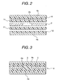
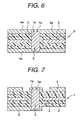
- the double-sided circuit board 1 can be manufactured in the following way. That is, a bore 2a is first opened at a predetermined position (a position for the via 5 for filling the soldered electric conductor 5a) of the Ni-Fe alloy foil 2, as shown in Fig. 2. Then, the conductor layers 4a comprising a copper foil are pasted from both sides of the Ni-Fe alloy foil 2, using a polyimide adhesive sheet 11 (which is the insulating layer 3 for a substrate 8 as will be described later). Thus, the substrate 8 is fabricated as shown in Fig. 3. (Reference numeral 12 denotes a polyimide resin layer formed on one face of the conductor layer 4a in Fig. 2). Then, as shown in Fig.
- a through hole 1a which is smaller than a bore portion 2a is provided at a portion corresponding to the bore portion 2a of the Ni-Fe alloy foil 2 of the substrate 8.
- the conductor layers 4a on the both sides is subjected to electrolytic copper plating, to connect electrically the conductor layers 4a on both sides (see Fig. 6).
- the thermal expansion coefficient of a substrate 9 obtained in this way is susceptible to that of the Ni-Fe alloy which is a material for the core, and can be adjusted by changing the ratio of Ni-Fe and the thickness of foil.
- a circuit 4 is formed on each of the conductor layers 4a on both sides of the substrate 9, as shown in Fig. 6, to fabricate a double-sided circuit board 1 (see Fig. 7).
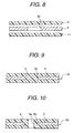
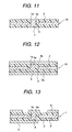
- the double-sided circuit board 1 can be also manufactured in the following way. That is, the bore 2a is first opened at a predetermined position (a position for the via 5 for filling the soldered electric conductor 5a) of the Ni-Fe alloy foil 2, as shown in Fig. 8. Then, the polyimide adhesive sheet 11 (which is the insulating layer 3 for a substrate 18 as will be described later) is pasted from either side of the Ni-Fe alloy foil 2, to fabricate the substrate 18 as shown in Fig. 9. Then, as shown in Fig. 10, the through hole 1a which is smaller than the bore portion 2a is provided at a portion corresponding to the bore portion 2a of the Ni-Fe alloy foil 2 of the substrate 18. Then, as shown in Fig.
- the conductor layers 4a comprising the copper foil are pasted from both sides to connect electrically the conductor layers 4a on both sides (see Fig. 12).
- the substrate is subjected to application of heat and pressure above a melting point of the soldered electric conductor 5a for the secure connection.
- the circuit 4 is formed on each of the conductor layers 4a on both sides of the substrate 19, as shown in Fig 12, to fabricate the double-sided circuit board 1 (see Fig. 13).
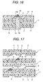
- the multi-layer wiring board can be manufactured in the following way. That is, three double-sided circuitboard 1 (see Fig. 7 or Fig. 13) having the circuit 4 comprising the copper foil formed on both sides of the insulating layer 3 made of polyimide resin, and two adhesive sheets 13 (see Fig. 14) made of polyimide adhesive are prepared. Then, as shown in Fig. 15, each adhesive sheet 13 is bonded temporarily on the upper face of two (of three) double-sided circuit boards 1, so that a bore portion 13a of each adhesive sheet 13 is registered at a predetermined position (a position for the soldered electric conductor 7 in Fig. 1) of the circuit 4 on each of the double-sided circuit boards 1. Then, as shown in Fig.
- a solder paste is poured into the bore portion 13a of each of the adhesive sheets 13 by screen printing and molten by heat to form the solder bump 14 on the circuit 4 of each of the double-sided circuit boards 1.
- two double-sided circuit boards 1 provided with the solder bump 4 and one double-sided circuit board 1 simply formed with the circuit 4 are laid one on the other (see Fig. 17) in registration, and integrated by application of heat and pressure.
- each adhesive sheet 13 becomes the adhesive layer 6
- each solder bump 14 becomes the soldered electric conductor 7.
- a six-layer wiring board having three double-sided circuit boards 1 laminated and integrated can be obtained.
- three double-sided circuit boards 1 can be integrated by application of heat and pressure at a time, and at the same time the electrical connection between six layers can be made.
- the Ni-Fe alloy foil 2 is disposed at a ratio of one layer to two layers of the circuit 4. Therefore, when the circuit 4 is constructed by the copper foil, the thermal expansion coefficient of the overall six-layer wiring board can be reduced, leading to an extremely high reliability. Since the soldered electric conductor 5a, 7 is used for the six-layer electrical connection (electrical connection between six layers), the connection resistance is low, leading to a high reliability connection. Further, the position of junction of each soldered electric conductor 7 is not susceptible to that of the soldered electric conductor 5a of the via 5, and can be placed at any position, leading to higher degree of freedom and higher wiring density.
- a copper foil 4a having a thickness of 18 ⁇ m was bonded by application of heat and pressure (40kg/cm2, 200°C, 60min), using a polyimide adhesive sheet 11 (manufactured by Nippon Steel Chemical: SPB-035A) having a thickness of 35 ⁇ m, on both sides of a 36 alloy foil 2 (Ni: 36 wt%, Fe: 64wt%, thermal expansion coefficient: 1.5ppm/°C) having a thickness of 50 ⁇ m, with a bore 2a opened at a predetermined position at a pitch of 300 ⁇ m by a punch 150 ⁇ m in diameter, thereby fabricating a low thermal expansion double-sided circuit board 8 (see Fig. 3).
- a through bore 1a was opened at the same position as the bore 2a of the 36 alloy foil 2, using a punch 100 ⁇ m in diameter (see Fig. 4).
- the upper portion of the through hole 1a was subjected to screen printing of a solder powder (with an average particle diameter of 10 ⁇ m), using metal mask (200 ⁇ m in diameter, 100 ⁇ m in thickness), and the solder powder was fitted into it by a press (100kg/cm2, 30°C, 5min). Then, an excess amount of solder was removed by buffing to provide a soldered via 5 (see Fig. 5). Thereafter, it was subjected to electrolytic copper plating with a plating thickness of 10 ⁇ m (see Fig. 6).
- a circuit 4 was formed on the copper foil 4a on both sides by the conventional etching method to fabricate a double-sided circuit board 1 (see Fig. 7).
- a polyimide adhesive sheet 13 manufactured by Nippon Steel Chemical: SPB-035A (manufactured by Nippon Steel Chemical: SPB-035A) (see Fig. 14) having a bore 13a opened by a punch 150 ⁇ m in diameter was laid at a predetermined position. In this state, they were bonded by application of heat and pressure (20kg/cm2, 175°C, 30min) (see Fig. 15). Then, a solder paste (made by Tamura Kaken: SQ10-11) was filled into the bore portion 13a of the adhesive sheet 13 by screen printing, and reflowed at a temperature of 220°C to clean and remove the flux to fabricate a solder bump 14 (see Fig. 16).
- a copper foil 4a having a thickness of 18 ⁇ m was bonded by application of heat and pressure (40kg/cm2, 200°C, 60min) (see Fig. 8), using a polyimide adhesive sheet 11 (manufactured by Nippon Steel Chemical: SPB-035A) having a thickness of 35 ⁇ m, on both sides of a 36 alloy foil 2 (Ni: 36 wt%, Fe: 64wt%, thermal expansion coefficient: 1.5ppm/°C) having a thickness of 50 ⁇ m, with a bore 2a opened at a predetermined position at a pitch of 300 ⁇ m by a punch 150 ⁇ m in diameter, thereby fabricating a low thermal expansion double-sided circuit board 18 (see Fig. 9).
- a through bore 1a was opened at the same position as the bore 2a of the 36 alloy foil 2, using a punch 100 ⁇ m in diameter (see Fig. 10).
- the upper portion of the through hole 1a was subjected to screen printing of a solder powder (with an average particle diameter of 10 ⁇ m), using a metal mask (200 ⁇ m in diameter, 100 ⁇ m in thickness), and the solder powder was fitted into it by a press (100kg/cm2, 30°C, 5min). Then, an excess amount of solder was removed by buffing to provide a soldered via 5 (see Fig. 11).
- a copper foil 4a having a thickness of 18 ⁇ m was bonded by application of heat and pressure (40kg/cm2, 200°C, 60min) on both sides of the low thermal expansion circuit board 18.
- a circuit 4 was formed on the copper foil 4a on both sides by the conventional etching method to fabricate a double-sided circuit board 1 (see Fig. 13).
- an adhesive sheet 13 was bonded temporarily on the double-sided circuit board, and a solder bump 14 was then formed.
- the double-sided circuit board was integrated by application of heat and pressure, and the electrical connection was made between layers. As a result, a low thermal expansion multi-layer wiring board of six-layer structure was fabricated.
- a polyimide adhesive sheet 11 (manufactured by Nippon Steel Chemical: SPB-035A) having a thickness of 35 ⁇ m was bonded by application of heat and pressure on both sides of a 36 alloy foil 2 (Ni: 36 wt%, Fe: 64wt%, thermal expansion coefficient: 1.5ppm/°C) having a thickness of 50 ⁇ m, with a bore 2a opened at a predetermined position at a pitch of 300 ⁇ m by a punch 150 ⁇ m in diameter, thereby fabricating a low thermal expansion double-sided circuit board 18 (see Fig. 9). Then, a through bore 1a was opened at the same position as the bore 2a of the 36 alloy foil 2, using a punch 100 ⁇ m in diameter.
- the upper portion of the through hole 1a was subjected to screen printing of an electrically conductive paste, and cured (175°C, 60min) to provide an electrically conductive via 15 (see Fig. 18).
- the electrically conductive paste was a mixture of a globular copper powder having an average particle diameter of 5 ⁇ m as an electrically conductive filler, a thermosetting epoxy resin as a resin, and an acid anhydride as a curing agent at a ratio of 85wt%, 12.5wt% and 2.5wt%.
- a copper foil 4a having a thickness of 18 ⁇ m was bonded by application of heat and pressure (40kg/cm2, 200°C, 60min) on both sides of the low thermal expansion circuit board.
- a circuit 4 was formed on the copper foil 4a on both sides by the conventional etching method to fabricate a double-sided circuit board 1.
- an adhesive sheet 13 was bonded temporarily on the double-sided circuit board, and a solder bump 14 was formed.
- the double-sided circuit board was integrated by application of heat and pressure, and the electrical connection between layers was made. As a result, a low thermal expansion multi-layer wiring board of six-layer structure was fabricated.
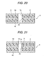
- a copper foil 4a having a thickness of 18 ⁇ m was bonded by application of heat and pressure, using a polyimide adhesive sheet 11 (manufactured by Nippon Steel Chemical: SPB-035A) having a thickness of 35 ⁇ m, on both sides of a 36 alloy foil 2 (Ni: 36 wt%, Fe: 64wt%, thermal expansion coefficient: 1.5ppm/°C) having a thickness of 50 ⁇ m, with a bore 2a opened at a predetermined position at a pitch of 300 ⁇ m by a punch 150 ⁇ m in diameter, thereby fabricating a low thermal expansion double-sided circuit board 8 (see Fig. 19).
- a through bore 1a was opened at the same position as the bore 2a of the 36 alloy foil 2, using a punch 100 ⁇ m in diameter (see Fig. 20). Then, the through-hole was plated by copper with a thickness of plating of 10 ⁇ m (forming a through-hole plating portion 16), as shown in Fig. 21.
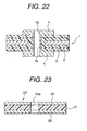
- a circuit 4 was formed on the copper foil 4a on both sides by the conventional etching method to fabricate a double-sided circuit board 1 (see Fig. 22).
- an adhesive sheet 13 was bonded temporarily on the double-sided circuit board, and a solder bump 14 was formed.
- the double-sided circuit board was integrated by application of heat and pressure, and the electrical connection between layers was made. As a result, a low thermal expansion multi-layer wiring board of six-layer structure was fabricated.
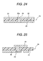
- a through hole 23a was opened by a punch ⁇ m in diameter (see Fig. 23) . Then, in the same way as the above examples, a soldered via 24 was provided (see Fig. 24), and then plated.
- a circuit 25 was formed to fabricate a double-sided circuit board 26 (see Fig. 25).
- an adhesive sheet 13 was bonded temporarily on the double-sided circuit board 26, and a solder bump 14 was formed.
- the double-sided circuit board 26 was integrated by application of heat and pressure, and the electrical connection between layers was made, in the same way as the above examples, thereby fabricating a low thermal expansion multi-layer wiring board of six-layer structure.
- a six-layer wiring board was fabricated in the same way as in the comparative example 3, except for using the electrically conductive via 15 of the comparative example 1, instead of providing the soldered via 24 used in the comparative example 3.
- a thermal shock test (liquid layer: -65°C to 150°C, each 5min) was conducted to make assessment of the electrical bonding reliability for each via 5, 15, 24 in the six-layer wiring board fabricated above, as described in the examples 1, 2 and the comparative examples 1 to 4.
- a table 1 below indicates the number of cycles at which a continuity failure has occurred in each via 5, 15, and 24. Herein, the variation in resistance beyond ⁇ 10% was considered as the continuity failure.
- TABLE 1 Thermal shock test (cyc.)
- the variation in continuity resistance is maintained within ⁇ 10% even after 2000 cycles in the examples 1 and 2 where the Ni-Fe alloy foil 2 is used as the core. Since the Ni-Fe alloy foil 2 can suppress the amount of variation in the Z-axis direction around the via 15, it is considered that the reliability in any cases of the examples 1 and 2 and the comparative example 1 was improved.
- the connection between any layers can be made by each minute via 5, 15, and 24, leading to a higher degree of freedom. As a result, it is clear that the higher wiring density can be easily realized.
- the insulating layer of the double-sided circuit board 1 contains a low thermal expansion core material comprising Ni-Fe alloy foil 2 at a ratio of one layer to the conductor layer 4a.
- the thermal expansion coefficient of the six-layer wiring board as described in the examples 1, 2 and the comparative examples 1 to 4 was measured in a range from room temperature (25°C) to 200°C. The results were listed in a table 2 below. TABLE 2 Thermal expansion coefficient (ppm/°C) Example 1 4.0 Example 2 4.0 Comparative example 1 4.0 Comparative example 2 4.0 Comparative example 3 17.0 Comparative example 4 17.0
- the thermal expansion coefficients of the six-layer wiring boards in the examples 1, 2 and the comparison examples 1, 2 which use Ni-Fe alloy foil 2 as the core material are extremely small. It is clear that these six-layer wiring boards are appropriate for the bare chip mounting. In this way, it is needless to say that the low thermal expansion coefficient multi-layer wiring board is appropriate for the bare chip mounting and is highly reliable in the electrical connection.
- the multi-layer wiring board of the present invention is provided with the via hole with the low melting point metal filled therein, instead of the through hole, and produces no crack inside or at the corner of the via hole in the environmental accelerated test such as temperature cycle test to be highly reliable in the electrical connection.
- Two double-sided circuit boards laid one on the other can be electrically connected by providing the soldered conductor on the via hole with the low melting metal filled therein, and has a great degree of freedom of wiring.
- the adhesive sheet is registered and bonded temporarily on the double-sided circuit board, the bore portion in this adhesive sheet is formed with the solder bump, and the double-sided circuit boards are laminated in registration and integrated by application of heat and pressure. Therefore, a plurality of double-sided circuit boards can be integrated by application of heat and pressure at a time.
- the electrical connection between wiring conductors can be made by application of heat and pressure at a time, irrespective of the number of layers of the wiring conductor.
Landscapes
- Engineering & Computer Science (AREA)
- Manufacturing & Machinery (AREA)
- Microelectronics & Electronic Packaging (AREA)
- Production Of Multi-Layered Print Wiring Board (AREA)
- Printing Elements For Providing Electric Connections Between Printed Circuits (AREA)
Claims (4)
- Mehrschichtige Verdrahtungsplatte, die umfasst:eine Vielzahl doppelseitiger Leiterplatten (1), wobei jede der Vielzahl doppelseitiger Leiterplatten (1) einen Metallkern (2) als Grundsubstanz, eine isolierende Schicht (3), die um den Metallkern (2) herum vorhanden ist, wobei die isolierende Schicht (3) ein organisches Harz mit hohem Molekulargewicht umfasst, und Verdrahtungsleiter (4) umfasst, die auf den beiden Seiten der isolierenden Schicht (3) vorhanden sind und elektrisch über ein Kontaktloch (5) verbunden sind, das sich in der doppelseitigen Leiterplatte (1) öffnet, und das Durchgangsloch (5) mit einem Metall (5a) mit niedrigem Schmelzpunkt gefüllt ist; undeine Klebeschicht (6), die zwischen zwei aneinandergrenzenden doppelseitigen Leiterplatten (1) vorhanden ist,wobei die Vielzahl der doppelseitigen Leiterplatten (1) über die Klebeschicht (6) als ein Stück laminiert sind, die Klebeschicht (6) eine Bohrung aufweist, die sich an einer vorgegebenen Position öffnet, die einem Abschnitt entspricht, der in direktem Kontakt mit den Verdrahtungsleitern (4) zwischen den zwei aneinandergrenzenden doppelseitigen Leiterplatten (1) sein soll, der Bohrungsabschnitt mit einem gelöteten elektrischen Leiter (7) versehen ist und die zwei doppelseitigen Leiterplatten (1) durch den gelöteten elektrischen Leiter (7) elektrisch verbunden sind,dadurch gekennzeichnet, dassdas Metall (5a) mit niedrigem Schmelzpunkt ein gelöteter elektrischer Leiter ist, der wenigstens eine Art Metall umfasst, das aus Sn, Pb, Ag, Bi, Zn, Sb und Cu ausgewählt wird, und sich das Metall mit niedrigem Schmelzpunkt über den gesamten Raum des Durchgangslochs (5) erstreckt.
- Mehrschichtige Leiterplatte nach Anspruch 1, wobei der Metallkern (2) eine Metallfolie, die Fe, Ni, Al, Ti, Cu oder Co umfasst, oder eine Metallfolie ist, die eine Legierung umfasst, die wenigstens zwei Elemente von Fe, Ni, Al, Ti, Cu oder Co umfasst.
- Mehrschichtige Leiterplatte nach Anspruch 1, wobei der Metallkern (2) eine Ni-Fe-Legierungsfolie ist, der Gehalt an Ni 31 bis 50 Gew.-% beträgt und der Metallkern (2) eine Dicke von 10 µm bis 100 µm hat.
- Verfahren zum Herstellen einer mehrschichtigen Verdrahtungsplatte nach Anspruch 1, das die folgenden Schritte umfasst:Herstellen einer Vielzahl doppelseitiger Leiterplatten (1) und einer Klebelage (6);wobei jede der Vielzahl doppelseitiger Leiterplatten (1) einen Metallkern (2) als Grundsubstanz, eine isolierende Schicht (3), die um den Metallkern (2) herum vorhanden ist, wobei die isolierende Schicht (3) ein organisches Harz mit hohem Molekulargewicht umfasst, und Verdrahtungsleiter (4) umfasst, die auf den beiden Seiten der isolierenden Schicht (3) vorhanden sind und elektrisch mit einem Durchgangsloch (5) verbunden sind, das sich in der doppelseitigen Leiterplatte (1) öffnet, und das Kontaktloch (5) mit einem gelöteten elektrischen Leiter gefüllt ist, der wenigstens eine Art Metall mit niedrigem Schmelzpunkt, das aus Sn, Pb, Ag, Bi, Zn, Sb und Cu ausgewählt wird, so umfasst, dass sich das Metall mit niedrigem Schmelzpunkt über den gesamten Raum des Kontaktlochs (5) erstreckt, und die Klebelage (6) eine Bohrung hat, die sich an einer Position öffnet, die einem vorgegebenen Abschnitt des Verdrahtungsleiters (4) der doppelseitigen Leiterplatte (1) entspricht,Ausbilden eines Lötkontakthügels (7) an dem Bohrungsabschnitt durch Einfüllen einer Lotpaste in den Bohrungsabschnitt jeder Klebelage (6) durch Drucken und Schmelzen der Lotpaste durch Erwärmen nach vorübergehendem Bonden der Klebelage (6); undLaminieren der Vielzahl der doppelseitigen Leiterplatten (1) als ein Stück über die Klebelage (6) durch Einwirkung von Wärme und Druck, wobei die Verdrahtungsleiter (4) jeder der Vielzahl der doppelseitigen Leiterplatten (1) nach Ausbilden des Lötkontakthügels so ausgerichtet sind, dass die vorgegebenen elektrischen Verbindungen möglich sind.
Applications Claiming Priority (2)
| Application Number | Priority Date | Filing Date | Title |
|---|---|---|---|
| JP19969099 | 1999-07-14 | ||
| JP19969099A JP4201436B2 (ja) | 1999-07-14 | 1999-07-14 | 多層配線基板の製造方法 |
Publications (3)
| Publication Number | Publication Date |
|---|---|
| EP1069811A2 EP1069811A2 (de) | 2001-01-17 |
| EP1069811A3 EP1069811A3 (de) | 2003-05-07 |
| EP1069811B1 true EP1069811B1 (de) | 2006-11-29 |
Family
ID=16412001
Family Applications (1)
| Application Number | Title | Priority Date | Filing Date |
|---|---|---|---|
| EP00115237A Expired - Lifetime EP1069811B1 (de) | 1999-07-14 | 2000-07-13 | Mehrschichtige Leiterplatte und Verfahren zu deren Herstellung |
Country Status (5)
| Country | Link |
|---|---|
| US (1) | US6335076B1 (de) |
| EP (1) | EP1069811B1 (de) |
| JP (1) | JP4201436B2 (de) |
| DE (1) | DE60032067T2 (de) |
| TW (1) | TW493367B (de) |
Families Citing this family (23)
| Publication number | Priority date | Publication date | Assignee | Title |
|---|---|---|---|---|
| US6159586A (en) * | 1997-09-25 | 2000-12-12 | Nitto Denko Corporation | Multilayer wiring substrate and method for producing the same |
| US20040094771A1 (en) * | 2001-03-26 | 2004-05-20 | Adolf Bernds | Device with at least two organic electronic components and method for producing the same |
| JP3461172B2 (ja) * | 2001-07-05 | 2003-10-27 | 日東電工株式会社 | 多層配線回路基板の製造方法 |
| JP2003023248A (ja) | 2001-07-05 | 2003-01-24 | Nitto Denko Corp | 多層フレキシブル配線回路基板およびその製造方法 |
| US6459047B1 (en) * | 2001-09-05 | 2002-10-01 | International Business Machines Corporation | Laminate circuit structure and method of fabricating |
| US6899815B2 (en) * | 2002-03-29 | 2005-05-31 | Intel Corporation | Multi-layer integrated circuit package |
| US20050233161A1 (en) * | 2002-04-02 | 2005-10-20 | Masaaki Takeda | Thermosetting adhesive sheet with electroconductive and thermoconductive properties |
| JP2003332752A (ja) * | 2002-05-14 | 2003-11-21 | Shinko Electric Ind Co Ltd | メタルコア基板およびその製造方法 |
| US7485812B2 (en) * | 2002-06-27 | 2009-02-03 | Ppg Industries Ohio, Inc. | Single or multi-layer printed circuit board with improved via design |
| US7358289B2 (en) * | 2002-10-22 | 2008-04-15 | 3M Innovative Properties Company | Heat-curable adhesive composition |
| JP2006024751A (ja) * | 2004-07-08 | 2006-01-26 | Three M Innovative Properties Co | 平面多導体の接続方法及び該接続方法で接続される部分を含む電気電子部品 |
| KR100632560B1 (ko) * | 2004-08-05 | 2006-10-09 | 삼성전기주식회사 | 병렬적 인쇄회로기판 제조 방법 |
| JP4287458B2 (ja) * | 2005-11-16 | 2009-07-01 | サムソン エレクトロ−メカニックス カンパニーリミテッド. | ペーストバンプを用いた印刷回路基板およびその製造方法 |
| EP2129201B1 (de) * | 2007-03-01 | 2017-04-12 | Murata Manufacturing Co. Ltd. | Mehrschichtiges schaltungssubstrat |
| CN101470298B (zh) | 2007-12-29 | 2012-01-11 | 富士迈半导体精密工业(上海)有限公司 | 背光模组 |
| CN101937852B (zh) * | 2010-08-19 | 2012-07-04 | 日月光半导体制造股份有限公司 | 线路基板制造方法 |
| US8921703B2 (en) * | 2012-02-17 | 2014-12-30 | Htc Corporation | Circuit board, structural unit thereof and manufacturing method thereof |
| KR101438915B1 (ko) * | 2012-11-02 | 2014-09-11 | 엘지이노텍 주식회사 | 인쇄회로기판 및 그의 제조 방법 |
| US20150122532A1 (en) * | 2013-11-04 | 2015-05-07 | Teledyne Technologies Incorporated | High temperature multilayer flexible printed wiring board |
| US10455708B2 (en) | 2015-06-29 | 2019-10-22 | Samsung Electro-Mechanics Co., Ltd. | Multilayered substrate and method for manufacturing the same |
| US9832866B2 (en) * | 2015-06-29 | 2017-11-28 | Samsung Electro-Mechanics Co., Ltd. | Multilayered substrate and method of manufacturing the same |
| JP7381323B2 (ja) * | 2019-12-17 | 2023-11-15 | 日東電工株式会社 | 両面配線回路基板の製造方法および両面配線回路基板 |
| CN111182713A (zh) * | 2020-01-15 | 2020-05-19 | 深圳市信维通信股份有限公司 | 高频线路板及其制作方法 |
Family Cites Families (8)
| Publication number | Priority date | Publication date | Assignee | Title |
|---|---|---|---|---|
| GB1310880A (en) * | 1969-06-13 | 1973-03-21 | Microponent Dev Ltd | Multi-layer printed circuit board assemblies |
| JPS61212096A (ja) | 1985-03-18 | 1986-09-20 | 株式会社日立製作所 | 多層配線板 |
| JPS62251136A (ja) * | 1986-04-25 | 1987-10-31 | 三菱樹脂株式会社 | 金属複合積層板 |
| US4942076A (en) * | 1988-11-03 | 1990-07-17 | Micro Substrates, Inc. | Ceramic substrate with metal filled via holes for hybrid microcircuits and method of making the same |
| JPH05259600A (ja) | 1992-03-11 | 1993-10-08 | Hitachi Chem Co Ltd | 配線板およびその製造法 |
| JPH0697665A (ja) | 1992-09-14 | 1994-04-08 | Toshiba Corp | 多層印刷配線基板の製造方法 |
| JPH06268381A (ja) | 1993-03-11 | 1994-09-22 | Hitachi Ltd | 多層配線構造体及びその製造方法 |
| US6159586A (en) * | 1997-09-25 | 2000-12-12 | Nitto Denko Corporation | Multilayer wiring substrate and method for producing the same |
-
1999
- 1999-07-14 JP JP19969099A patent/JP4201436B2/ja not_active Expired - Fee Related
-
2000
- 2000-07-13 DE DE60032067T patent/DE60032067T2/de not_active Expired - Lifetime
- 2000-07-13 EP EP00115237A patent/EP1069811B1/de not_active Expired - Lifetime
- 2000-07-13 US US09/615,761 patent/US6335076B1/en not_active Expired - Lifetime
- 2000-07-14 TW TW089114072A patent/TW493367B/zh not_active IP Right Cessation
Also Published As
| Publication number | Publication date |
|---|---|
| TW493367B (en) | 2002-07-01 |
| JP4201436B2 (ja) | 2008-12-24 |
| EP1069811A2 (de) | 2001-01-17 |
| DE60032067D1 (de) | 2007-01-11 |
| JP2001028482A (ja) | 2001-01-30 |
| US6335076B1 (en) | 2002-01-01 |
| EP1069811A3 (de) | 2003-05-07 |
| DE60032067T2 (de) | 2007-03-08 |
Similar Documents
| Publication | Publication Date | Title |
|---|---|---|
| EP1069811A2 (de) | Mehrschichtige Leiterplatte und Verfahren zu deren Herstellung | |
| US8942003B2 (en) | Multilayered printed wiring board | |
| US6373000B2 (en) | Double-sided circuit board and multilayer wiring board comprising the same and process for producing double-sided circuit board | |
| EP1611611B1 (de) | Verfahren zur herstellung von 3-d verbindungsstrukturen, die völlig organisch sind | |
| US7102085B2 (en) | Wiring substrate | |
| EP1250033B1 (de) | Leiterplatte und Elektronikkomponente | |
| US6359235B1 (en) | Electrical device mounting wiring board and method of producing the same | |
| KR100517009B1 (ko) | 다층배선기판및이의제조방법 | |
| EP1132962A2 (de) | Leiterplatte, Halbleiter und Herstellung | |
| WO2007126090A1 (ja) | 回路基板、電子デバイス装置及び回路基板の製造方法 | |
| JPH11312868A (ja) | 素子内蔵多層配線基板およびその製造方法 | |
| JP3634984B2 (ja) | 配線基板 | |
| JP2002076637A (ja) | チップ部品内蔵基板及びその製造方法 | |
| CN1874648B (zh) | 布线板以及布线板的制造方法 | |
| EP1956877B1 (de) | Mehrschichtige Leiterplatte und Herstellungsverfahren dafür | |
| JP5192865B2 (ja) | 部品内蔵配線基板の製造方法 | |
| JPH10190232A (ja) | 多層配線基板及びその製造方法 | |
| JP2002290052A (ja) | 多層配線基板 | |
| JP5170570B2 (ja) | 樹脂多層モジュール及び樹脂多層モジュールの製造方法 | |
| JP3574738B2 (ja) | 配線基板 | |
| JP4582938B2 (ja) | 絶縁シートの製造方法および配線基板の製造方法 | |
| JP2005038918A (ja) | 多層フレキシブルプリント配線板及びその製造方法 | |
| KR20050114189A (ko) | 적층 기판, 그 제조 방법 및 그 적층 기판을 갖는 전자기기 | |
| JPH11163522A (ja) | 多層配線基板およびその製造方法 | |
| JP2000223836A (ja) | 多層配線基板およびその製造方法 |
Legal Events
| Date | Code | Title | Description |
|---|---|---|---|
| PUAI | Public reference made under article 153(3) epc to a published international application that has entered the european phase |
Free format text: ORIGINAL CODE: 0009012 |
|
| AK | Designated contracting states |
Kind code of ref document: A2 Designated state(s): AT BE CH CY DE DK ES FI FR GB GR IE IT LI LU MC NL PT SE |
|
| AX | Request for extension of the european patent |
Free format text: AL;LT;LV;MK;RO;SI |
|
| PUAL | Search report despatched |
Free format text: ORIGINAL CODE: 0009013 |
|
| AK | Designated contracting states |
Designated state(s): AT BE CH CY DE DK ES FI FR GB GR IE IT LI LU MC NL PT SE |
|
| AX | Request for extension of the european patent |
Extension state: AL LT LV MK RO SI |
|
| 17P | Request for examination filed |
Effective date: 20030715 |
|
| 17Q | First examination report despatched |
Effective date: 20031111 |
|
| AKX | Designation fees paid |
Designated state(s): DE FR GB |
|
| GRAP | Despatch of communication of intention to grant a patent |
Free format text: ORIGINAL CODE: EPIDOSNIGR1 |
|
| GRAS | Grant fee paid |
Free format text: ORIGINAL CODE: EPIDOSNIGR3 |
|
| GRAA | (expected) grant |
Free format text: ORIGINAL CODE: 0009210 |
|
| AK | Designated contracting states |
Kind code of ref document: B1 Designated state(s): DE FR GB |
|
| REG | Reference to a national code |
Ref country code: GB Ref legal event code: FG4D |
|
| REF | Corresponds to: |
Ref document number: 60032067 Country of ref document: DE Date of ref document: 20070111 Kind code of ref document: P |
|
| ET | Fr: translation filed | ||
| PLBE | No opposition filed within time limit |
Free format text: ORIGINAL CODE: 0009261 |
|
| STAA | Information on the status of an ep patent application or granted ep patent |
Free format text: STATUS: NO OPPOSITION FILED WITHIN TIME LIMIT |
|
| 26N | No opposition filed |
Effective date: 20070830 |
|
| PGFP | Annual fee paid to national office [announced via postgrant information from national office to epo] |
Ref country code: GB Payment date: 20120711 Year of fee payment: 13 |
|
| PGFP | Annual fee paid to national office [announced via postgrant information from national office to epo] |
Ref country code: DE Payment date: 20120711 Year of fee payment: 13 Ref country code: FR Payment date: 20120719 Year of fee payment: 13 |
|
| GBPC | Gb: european patent ceased through non-payment of renewal fee |
Effective date: 20130713 |
|
| REG | Reference to a national code |
Ref country code: DE Ref legal event code: R119 Ref document number: 60032067 Country of ref document: DE Effective date: 20140201 |
|
| REG | Reference to a national code |
Ref country code: FR Ref legal event code: ST Effective date: 20140331 |
|
| PG25 | Lapsed in a contracting state [announced via postgrant information from national office to epo] |
Ref country code: GB Free format text: LAPSE BECAUSE OF NON-PAYMENT OF DUE FEES Effective date: 20130713 Ref country code: DE Free format text: LAPSE BECAUSE OF NON-PAYMENT OF DUE FEES Effective date: 20140201 |
|
| PG25 | Lapsed in a contracting state [announced via postgrant information from national office to epo] |
Ref country code: FR Free format text: LAPSE BECAUSE OF NON-PAYMENT OF DUE FEES Effective date: 20130731 |