EP1060285B1 - Vorrichtung und verfahren zur beschichtung von halbleitermaterial - Google Patents
Vorrichtung und verfahren zur beschichtung von halbleitermaterial Download PDFInfo
- Publication number
- EP1060285B1 EP1060285B1 EP99903204A EP99903204A EP1060285B1 EP 1060285 B1 EP1060285 B1 EP 1060285B1 EP 99903204 A EP99903204 A EP 99903204A EP 99903204 A EP99903204 A EP 99903204A EP 1060285 B1 EP1060285 B1 EP 1060285B1
- Authority
- EP
- European Patent Office
- Prior art keywords
- semiconductor material
- depositing
- glass sheet
- sheet substrate
- permeable member
- Prior art date
- Legal status (The legal status is an assumption and is not a legal conclusion. Google has not performed a legal analysis and makes no representation as to the accuracy of the status listed.)
- Expired - Lifetime
Links
- 239000004065 semiconductor Substances 0.000 title claims abstract description 121
- 239000000463 material Substances 0.000 title claims abstract description 106
- 238000000151 deposition Methods 0.000 title claims abstract description 65
- 238000000034 method Methods 0.000 title claims abstract description 27
- 239000000758 substrate Substances 0.000 claims abstract description 72
- 239000011521 glass Substances 0.000 claims abstract description 71
- 239000012159 carrier gas Substances 0.000 claims abstract description 43
- 230000008021 deposition Effects 0.000 claims abstract description 28
- 239000000843 powder Substances 0.000 claims abstract description 27
- 238000010438 heat treatment Methods 0.000 claims abstract description 12
- 239000007789 gas Substances 0.000 claims description 21
- 229910010293 ceramic material Inorganic materials 0.000 claims description 4
- KZHJGOXRZJKJNY-UHFFFAOYSA-N dioxosilane;oxo(oxoalumanyloxy)alumane Chemical compound O=[Si]=O.O=[Si]=O.O=[Al]O[Al]=O.O=[Al]O[Al]=O.O=[Al]O[Al]=O KZHJGOXRZJKJNY-UHFFFAOYSA-N 0.000 claims description 4
- 229910052863 mullite Inorganic materials 0.000 claims description 4
- 239000001307 helium Substances 0.000 claims description 3
- 229910052734 helium Inorganic materials 0.000 claims description 3
- SWQJXJOGLNCZEY-UHFFFAOYSA-N helium atom Chemical compound [He] SWQJXJOGLNCZEY-UHFFFAOYSA-N 0.000 claims description 3
- HBMJWWWQQXIZIP-UHFFFAOYSA-N silicon carbide Chemical compound [Si+]#[C-] HBMJWWWQQXIZIP-UHFFFAOYSA-N 0.000 claims description 3
- 229910010271 silicon carbide Inorganic materials 0.000 claims description 3
- 238000010276 construction Methods 0.000 description 8
- MARUHZGHZWCEQU-UHFFFAOYSA-N 5-phenyl-2h-tetrazole Chemical compound C1=CC=CC=C1C1=NNN=N1 MARUHZGHZWCEQU-UHFFFAOYSA-N 0.000 description 5
- XKRFYHLGVUSROY-UHFFFAOYSA-N Argon Chemical compound [Ar] XKRFYHLGVUSROY-UHFFFAOYSA-N 0.000 description 2
- IJGRMHOSHXDMSA-UHFFFAOYSA-N Atomic nitrogen Chemical compound N#N IJGRMHOSHXDMSA-UHFFFAOYSA-N 0.000 description 2
- 239000002699 waste material Substances 0.000 description 2
- PFNQVRZLDWYSCW-UHFFFAOYSA-N (fluoren-9-ylideneamino) n-naphthalen-1-ylcarbamate Chemical compound C12=CC=CC=C2C2=CC=CC=C2C1=NOC(=O)NC1=CC=CC2=CC=CC=C12 PFNQVRZLDWYSCW-UHFFFAOYSA-N 0.000 description 1
- WUPHOULIZUERAE-UHFFFAOYSA-N 3-(oxolan-2-yl)propanoic acid Chemical compound OC(=O)CCC1CCCO1 WUPHOULIZUERAE-UHFFFAOYSA-N 0.000 description 1
- OKTJSMMVPCPJKN-UHFFFAOYSA-N Carbon Chemical compound [C] OKTJSMMVPCPJKN-UHFFFAOYSA-N 0.000 description 1
- PNEYBMLMFCGWSK-UHFFFAOYSA-N aluminium oxide Inorganic materials [O-2].[O-2].[O-2].[Al+3].[Al+3] PNEYBMLMFCGWSK-UHFFFAOYSA-N 0.000 description 1
- 229910052786 argon Inorganic materials 0.000 description 1
- QVGXLLKOCUKJST-UHFFFAOYSA-N atomic oxygen Chemical compound [O] QVGXLLKOCUKJST-UHFFFAOYSA-N 0.000 description 1
- BDOSMKKIYDKNTQ-UHFFFAOYSA-N cadmium atom Chemical compound [Cd] BDOSMKKIYDKNTQ-UHFFFAOYSA-N 0.000 description 1
- 229910052980 cadmium sulfide Inorganic materials 0.000 description 1
- 229910052799 carbon Inorganic materials 0.000 description 1
- 238000000576 coating method Methods 0.000 description 1
- 238000004891 communication Methods 0.000 description 1
- 150000001875 compounds Chemical class 0.000 description 1
- 238000010924 continuous production Methods 0.000 description 1
- 229910052593 corundum Inorganic materials 0.000 description 1
- 239000002019 doping agent Substances 0.000 description 1
- 229910052743 krypton Inorganic materials 0.000 description 1
- DNNSSWSSYDEUBZ-UHFFFAOYSA-N krypton atom Chemical compound [Kr] DNNSSWSSYDEUBZ-UHFFFAOYSA-N 0.000 description 1
- 210000003141 lower extremity Anatomy 0.000 description 1
- 229910052754 neon Inorganic materials 0.000 description 1
- GKAOGPIIYCISHV-UHFFFAOYSA-N neon atom Chemical compound [Ne] GKAOGPIIYCISHV-UHFFFAOYSA-N 0.000 description 1
- 229910052757 nitrogen Inorganic materials 0.000 description 1
- 239000001301 oxygen Substances 0.000 description 1
- 229910052760 oxygen Inorganic materials 0.000 description 1
- 238000000859 sublimation Methods 0.000 description 1
- 230000008022 sublimation Effects 0.000 description 1
- 229910052714 tellurium Inorganic materials 0.000 description 1
- PORWMNRCUJJQNO-UHFFFAOYSA-N tellurium atom Chemical compound [Te] PORWMNRCUJJQNO-UHFFFAOYSA-N 0.000 description 1
- 210000001364 upper extremity Anatomy 0.000 description 1
- 238000007740 vapor deposition Methods 0.000 description 1
- 229910001845 yogo sapphire Inorganic materials 0.000 description 1
Images

Classifications
-
- C—CHEMISTRY; METALLURGY
- C23—COATING METALLIC MATERIAL; COATING MATERIAL WITH METALLIC MATERIAL; CHEMICAL SURFACE TREATMENT; DIFFUSION TREATMENT OF METALLIC MATERIAL; COATING BY VACUUM EVAPORATION, BY SPUTTERING, BY ION IMPLANTATION OR BY CHEMICAL VAPOUR DEPOSITION, IN GENERAL; INHIBITING CORROSION OF METALLIC MATERIAL OR INCRUSTATION IN GENERAL
- C23C—COATING METALLIC MATERIAL; COATING MATERIAL WITH METALLIC MATERIAL; SURFACE TREATMENT OF METALLIC MATERIAL BY DIFFUSION INTO THE SURFACE, BY CHEMICAL CONVERSION OR SUBSTITUTION; COATING BY VACUUM EVAPORATION, BY SPUTTERING, BY ION IMPLANTATION OR BY CHEMICAL VAPOUR DEPOSITION, IN GENERAL
- C23C14/00—Coating by vacuum evaporation, by sputtering or by ion implantation of the coating forming material
- C23C14/22—Coating by vacuum evaporation, by sputtering or by ion implantation of the coating forming material characterised by the process of coating
- C23C14/24—Vacuum evaporation
- C23C14/246—Replenishment of source material
-
- C—CHEMISTRY; METALLURGY
- C03—GLASS; MINERAL OR SLAG WOOL
- C03C—CHEMICAL COMPOSITION OF GLASSES, GLAZES OR VITREOUS ENAMELS; SURFACE TREATMENT OF GLASS; SURFACE TREATMENT OF FIBRES OR FILAMENTS MADE FROM GLASS, MINERALS OR SLAGS; JOINING GLASS TO GLASS OR OTHER MATERIALS
- C03C17/00—Surface treatment of glass, not in the form of fibres or filaments, by coating
- C03C17/001—General methods for coating; Devices therefor
- C03C17/002—General methods for coating; Devices therefor for flat glass, e.g. float glass
-
- C—CHEMISTRY; METALLURGY
- C03—GLASS; MINERAL OR SLAG WOOL
- C03C—CHEMICAL COMPOSITION OF GLASSES, GLAZES OR VITREOUS ENAMELS; SURFACE TREATMENT OF GLASS; SURFACE TREATMENT OF FIBRES OR FILAMENTS MADE FROM GLASS, MINERALS OR SLAGS; JOINING GLASS TO GLASS OR OTHER MATERIALS
- C03C17/00—Surface treatment of glass, not in the form of fibres or filaments, by coating
- C03C17/22—Surface treatment of glass, not in the form of fibres or filaments, by coating with other inorganic material
-
- C—CHEMISTRY; METALLURGY
- C23—COATING METALLIC MATERIAL; COATING MATERIAL WITH METALLIC MATERIAL; CHEMICAL SURFACE TREATMENT; DIFFUSION TREATMENT OF METALLIC MATERIAL; COATING BY VACUUM EVAPORATION, BY SPUTTERING, BY ION IMPLANTATION OR BY CHEMICAL VAPOUR DEPOSITION, IN GENERAL; INHIBITING CORROSION OF METALLIC MATERIAL OR INCRUSTATION IN GENERAL
- C23C—COATING METALLIC MATERIAL; COATING MATERIAL WITH METALLIC MATERIAL; SURFACE TREATMENT OF METALLIC MATERIAL BY DIFFUSION INTO THE SURFACE, BY CHEMICAL CONVERSION OR SUBSTITUTION; COATING BY VACUUM EVAPORATION, BY SPUTTERING, BY ION IMPLANTATION OR BY CHEMICAL VAPOUR DEPOSITION, IN GENERAL
- C23C14/00—Coating by vacuum evaporation, by sputtering or by ion implantation of the coating forming material
- C23C14/22—Coating by vacuum evaporation, by sputtering or by ion implantation of the coating forming material characterised by the process of coating
- C23C14/228—Gas flow assisted PVD deposition
-
- C—CHEMISTRY; METALLURGY
- C23—COATING METALLIC MATERIAL; COATING MATERIAL WITH METALLIC MATERIAL; CHEMICAL SURFACE TREATMENT; DIFFUSION TREATMENT OF METALLIC MATERIAL; COATING BY VACUUM EVAPORATION, BY SPUTTERING, BY ION IMPLANTATION OR BY CHEMICAL VAPOUR DEPOSITION, IN GENERAL; INHIBITING CORROSION OF METALLIC MATERIAL OR INCRUSTATION IN GENERAL
- C23C—COATING METALLIC MATERIAL; COATING MATERIAL WITH METALLIC MATERIAL; SURFACE TREATMENT OF METALLIC MATERIAL BY DIFFUSION INTO THE SURFACE, BY CHEMICAL CONVERSION OR SUBSTITUTION; COATING BY VACUUM EVAPORATION, BY SPUTTERING, BY ION IMPLANTATION OR BY CHEMICAL VAPOUR DEPOSITION, IN GENERAL
- C23C14/00—Coating by vacuum evaporation, by sputtering or by ion implantation of the coating forming material
- C23C14/22—Coating by vacuum evaporation, by sputtering or by ion implantation of the coating forming material characterised by the process of coating
- C23C14/24—Vacuum evaporation
-
- C—CHEMISTRY; METALLURGY
- C23—COATING METALLIC MATERIAL; COATING MATERIAL WITH METALLIC MATERIAL; CHEMICAL SURFACE TREATMENT; DIFFUSION TREATMENT OF METALLIC MATERIAL; COATING BY VACUUM EVAPORATION, BY SPUTTERING, BY ION IMPLANTATION OR BY CHEMICAL VAPOUR DEPOSITION, IN GENERAL; INHIBITING CORROSION OF METALLIC MATERIAL OR INCRUSTATION IN GENERAL
- C23C—COATING METALLIC MATERIAL; COATING MATERIAL WITH METALLIC MATERIAL; SURFACE TREATMENT OF METALLIC MATERIAL BY DIFFUSION INTO THE SURFACE, BY CHEMICAL CONVERSION OR SUBSTITUTION; COATING BY VACUUM EVAPORATION, BY SPUTTERING, BY ION IMPLANTATION OR BY CHEMICAL VAPOUR DEPOSITION, IN GENERAL
- C23C14/00—Coating by vacuum evaporation, by sputtering or by ion implantation of the coating forming material
- C23C14/22—Coating by vacuum evaporation, by sputtering or by ion implantation of the coating forming material characterised by the process of coating
- C23C14/56—Apparatus specially adapted for continuous coating; Arrangements for maintaining the vacuum, e.g. vacuum locks
-
- C—CHEMISTRY; METALLURGY
- C03—GLASS; MINERAL OR SLAG WOOL
- C03C—CHEMICAL COMPOSITION OF GLASSES, GLAZES OR VITREOUS ENAMELS; SURFACE TREATMENT OF GLASS; SURFACE TREATMENT OF FIBRES OR FILAMENTS MADE FROM GLASS, MINERALS OR SLAGS; JOINING GLASS TO GLASS OR OTHER MATERIALS
- C03C2217/00—Coatings on glass
- C03C2217/20—Materials for coating a single layer on glass
- C03C2217/28—Other inorganic materials
- C03C2217/287—Chalcogenides
-
- C—CHEMISTRY; METALLURGY
- C03—GLASS; MINERAL OR SLAG WOOL
- C03C—CHEMICAL COMPOSITION OF GLASSES, GLAZES OR VITREOUS ENAMELS; SURFACE TREATMENT OF GLASS; SURFACE TREATMENT OF FIBRES OR FILAMENTS MADE FROM GLASS, MINERALS OR SLAGS; JOINING GLASS TO GLASS OR OTHER MATERIALS
- C03C2218/00—Methods for coating glass
- C03C2218/10—Deposition methods
- C03C2218/15—Deposition methods from the vapour phase
- C03C2218/151—Deposition methods from the vapour phase by vacuum evaporation
Definitions
- This invention relates to apparatus and a method for depositing a semiconductor material on a glass sheet substrate.
- This construction requires that the source material troughs be periodically replenished with the cadmium telluride that provides the semiconductor material.
- the Foote et al. patent also disclose introduction of the source material as a vapor from sources of elemental cadmium and tellurium or from a source of cadmium telluride.
- One object of the present invention is to provide improved apparatus for depositing a semiconductor material on a glass sheet substrate.
- the preferred construction of the apparatus has the heated permeable member constructed with a tubular shape into which the material supply introduces the carrier gas and the semiconductor material for flow outwardly therefrom as the vapor that is deposited on the glass sheet substrate as the semiconductor layer.
- This tubular permeable member has opposite ends across which an electrical voltage is applied to provide its heating.
- the tubular permeable member is made of silicon carbide.
- the preferred construction of the apparatus also includes a shroud of a generally tubular shape that receives the tubular permeable member.
- This shroud has an opening through which the vapor passes for the deposition of the semiconductor layer on the glass sheet substrate.
- the opening of the shroud is a slit that extends along the tubular shape of the shroud.
- the shroud may have opposite ends between which the slit has a varying size to control the distribution of the vapor deposition onto the glass sheet substrate.
- the shroud is preferably made of a ceramic material that is disclosed as being mullite.
- the material supply introduces the carrier gas and semiconductor material into one end of the tubular permeable member
- the apparatus further includes another material supply that introduces the carrier gas and the semiconductor material into the other end of the tubular permeable member.
- Different embodiments of the apparatus are disclosed as including a gas passage into which the semiconductor material is introduced as a powder for flow with the carrier gas.
- Certain embodiments of the material supply include a rotary screw and the gas passage into which the rotary screw introduces the semiconductor material, with one of these embodiments having the rotary screw rotating about a horizontal axis, and with another of these embodiments having the rotary screw rotating about a vertical axis.
- a further embodiment of the apparatus includes a vibratory feeder and the gas passage into which the vibratory feeder introduces a powder of the semiconductor material for flow with the carrier gas.
- Each disclosed embodiment of the apparatus has the conveyor supporting the glass sheet substrate in a horizontally extending orientation so as to have downwardly and upwardly facing surfaces.
- One embodiment of the apparatus has the heated permeable member located above the conveyor to deposit the semiconductor layer on the upwardly facing surface of the glass sheet substrate.
- that embodiment is disclosed as including rolls that support the downwardly facing surface of the glass sheet substrate.
- Another embodiment of the apparatus has the conveyor constructed to include a gas hearth for supporting the glass sheet substrate in a generally horizontally extending orientation so as to have downwardly and upwardly facing surfaces.
- the heated permeable member of this latter embodiment is disclosed as being located below the glass sheet substrate to deposit the semiconductor layer on the downwardly facing surface of the glass sheet substrate.
- Another object of the present invention is to provide an improved method for depositing a semiconductor material on a glass sheet substrate.
- the method for depositing the semiconductor material is performed by heating a permeable member and by passing a carrier gas and a powdered semiconductor material through the heated permeable member for heating to provide a vapor.
- a glass sheet substrate is conveyed adjacent the heated permeable member for deposition of the vapor on the glass sheet substrate as a semiconductor layer.
- an electrical voltage is applied across opposite ends of the permeable member which has a tubular shape into which the carrier gas and the semiconductor material are introduced for passage outwardly therethrough as the vapor that is deposited on the glass sheet substrate as the semiconductor layer.
- the vapor is guided around the exterior of the tubular permeable member by a shroud and is passed outwardly through an opening in the shroud for the deposition on the glass sheet substrate as the semiconductor layer.
- the vapor may be passed outwardly from the shroud through a slit-shaped opening having opposite ends between which the opening has a varying size to control distribution of the deposition of the vapor on the glass sheet substrate as the semiconductor layer.
- the carrier gas and the semiconductor material are disclosed as both being introduced into opposite ends of the tubular permeable member.
- Different practices of the method have the semiconductor material introduced as a powder into the carrier gas for flow to and through the heated permeable member.
- the semiconductor powder is introduced into the carrier gas by a rotary screw, while another such practice of the method introduces the semiconductor powder into the carrier gas by a vibratory feeder.
- the method is performed using a carrier gas that is helium.
- Two different practices of the method are both performed by conveying the glass sheet substrate in a horizontally extending orientation so as to have downwardly and upwardly facing surfaces, with the vapor flowing downwardly for deposition of the semiconductor layer on the upwardly facing surface of the conveyed glass sheet substrate in one practice of the method, and with the vapor flowing upwardly for deposition of the semiconductor layer on the downwardly facing surface of the conveyed glass sheet substrate in the other practice of the method.
- a glass sheet processing system generally indicated by 10 includes apparatus 12 constructed according to the invention to perform the method of the invention. Both the apparatus 12 and the method for processing glass sheets G according to the invention will be hereinafter more fully described in an integrated manner to facilitate an understanding of the different aspects of the invention.
- the system 10 includes a housing 14 defining a processing chamber 16 in which a semiconductor material is deposited on glass sheet substrates G.
- Housing 14 includes an entry station 18 and an exit station 20. These entry and exit stations 18 and 20 can be constructed as load locks or as slit seals through which the glass sheet substrates G enter and exit the processing chamber 16.
- the housing 14 is heated in any suitable manner such as disclosed by the aforementioned Foote et al. patents such that its processing chamber is maintained at a temperature of 500° to 700°C, and the glass sheet substrates are heated during the processing to a slightly lower temperature of about 400° to 650°C.
- the apparatus 12 of the invention includes a distributor 22 having an electrically conductive permeable member 24 of a tubular shape having an elongated construction.
- the tubular permeable member 24 is heated, which as disclosed is performed by electrical connections 26 at its opposite ends 28 and application of a voltage along the length of the member. This voltage causes an electrical current to flow along the length of the tubular permeable member 24 so as to provide electrical heating thereof during the processing.
- This heating of the tubular permeable member 24 is to a temperature of about 850° to 1150°C.
- At least one material supply 30 of the apparatus 12 is provided for introducing a carrier gas and a semiconductor material into the tubular permeable member 24 for heating to provide a vapor that passes outwardly through the tubular permeable member during the processing.
- a conveyor 32 of the apparatus conveys a glass sheet substrate G adjacent the distributor 22 for deposition of the vapor on the substrate as a semiconductor layer.
- the tubular permeable member 24 is made of silicon carbide although it could also be made of permeable carbon or any other permeable material that is preferably electrically conductive to provide the heating in the manner disclosed.
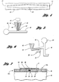
- the distributor 22 preferably includes a shroud 34 of a generally tubular shape that receives the tubular permeable member 24 as best illustrated in Figure 3 .
- the shroud 34 guides the vapor around the exterior of the tubular permeable member 24 and has an opening 36 through which the vapor passes for the deposition of the semiconductor layer on the glass sheet substrate G. More specifically, the preferred construction of the shroud 34 has the opening 34 constructed as a slit that extends along the tubular shape of the shroud.
- the shroud 34 as shown in Figure 4 has opposite ends 37 between which the slit-shaped opening 36 has a varying size which facilitates distribution of the vapor and uniform deposition of the semiconductor layer. More specifically, the slit-shaped opening 36 has a smaller size adjacent the ends 37 where the carrier gas and semiconductor material are introduced, as is hereinafter more fully described, and has a larger size at the central more remote area from that introduction so as to provide the uniform deposition. To provide good distribution of the semiconductor material, it may be desirable to provide the interior of the tubular permeable member 24 with a suitable diverter that provides a uniform passage of the vapor outwardly along the length of the tubular permeable member and then along the length of the slit-shaped opening 36 of the shroud. Furthermore, the shroud 34 is preferably made of a ceramic material that is most preferably mullite.
- the shroud 34 also advantageously reduces radiant heat transfer from the hot tubular permeable member 24 to the glass sheet substrate G. More specifically, the amount of energy the shroud 34 radiates to the glass sheet substrate is reduced because its outside surface temperature is lower than that of the hot tubular permeable member 24.
- Mullite has an adequately low emissivity and is relatively strong and easy to fabricate.
- coatings can be provided to lower the emissivity of the outer surface of the shroud 34 such as Al 2 O 3 or Y 2 O 3 .
- the length of the slit-shaped opening 36 of the shroud 34 can be selected to control the extent of the width of the deposited layer on the glass sheet substrate.
- the length of the split-shaped opening 36 can be selected to be less than the width of the glass sheet substrate to provide a strip of the deposited layer. Such control can also minimize waste of the vapors.
- the entire width of the substrate is to be covered, one can ideally make the length of the slit-shaped opening 36 equal to or slightly less than the width of the substrate such that the substantially all of the vapors are deposited onto the substrate during the deposition.
- the shroud 34 has been spaced from the conveyed glass sheet substrate a distance in the range of 0.5 to 3.0 centimeters. While greater spacings could be utilized, that would require lower system pressures and would result in vapor waste due to overspraying. Furthermore, smaller spacing could cause problems due to thermal warpage of the glass sheet substrate during conveyance.
- the material supply 30 introduces a carrier gas from a source 38 and a semiconductor material as a powder 40 from a hopper 42 into one end 28 of the tubular permeable member 24, and there is also another material supply 30 that likewise introduces a carrier gas and a semiconductor material as a powder into the other end 28 of the tubular permeable member 24.
- a carrier gas from a source 38 and a semiconductor material as a powder 40 from a hopper 42 into one end 28 of the tubular permeable member 24
- another material supply 30 that likewise introduces a carrier gas and a semiconductor material as a powder into the other end 28 of the tubular permeable member 24.
- each of the material supplies 30 illustrated includes a rotary screw 44 that receives the semiconductor powder 40 from the hopper 42 and is rotatively driven by a suitable actuator 46.
- a passage 48 extends from the carrier gas source 38 to the adjacent end 28 of the porous tubular member 24 in communication with the rotary screw 44. Rotation of the screw 44 at a controlled rate introduces the semiconductor powder 40 into the passage 48 so as to be entrained therein for flow into the tubular permeable member 24 for the heating that provides the vapor.
- Figures 2 , 5 and 6 respectively disclose different embodiments of the material supplies 30, 30' and 30". More specifically, the embodiment of the material supply 30 illustrated in Figure 2 has the screw 44 rotated about a horizontal axis for introduction of the semiconductor powder 40 into the carrier gas passage 48, while the Figure 5 embodiment of the material supply 30' has the screw 44 rotated about a vertical axis for introduction of the semiconductor powder 40 from the hopper 42 into the carrier gas passage 48. With each of these screw embodiments of the material supplies, the amount of semiconductor material introduced as a powder can be accurately controlled by the rate of screw rotation. Furthermore, the Figure 6 embodiment of the material supply 30" includes a vibratory feeder 50 having an inclined passage 52 extending upwardly from the hopper 42 to the carrier gas passage 48. Operation of the vibratory feeder 50 causes vibration of the semiconductor powder 40 which moves it upwardly along the inclined passage 52 to the carrier gas passage 48 for flow as an entrained powder into the tubular permeable member 24.
- a vibratory feeder 50 having an inclined passage 52 extending upwardly from the hopper 42 to the carrier
- the semiconductor powder can also be utilized for feeding the semiconductor powder including fluidized bed feeders and rotary disk feeders that are commercially available.
- the powder feed rate and the speed of conveyance of the glass sheet substrate directly control the film thickness such that the carrier gas flow rate, powder feed rate, and glass sheet conveyance speed all must be controlled. Also, starting and stopping of the powder feed can be utilized to commence and terminate the deposition of the semiconductor layer on the glass sheet substrate.
- Two different embodiments of the apparatus 12 and 12a respectively illustrated by Figures 1 and 7 both support the glass sheet substrate G in a horizontally extending orientation so as to have downwardly and upwardly facing surfaces 54 and 56.
- the distributor 22 is located above the conveyor 32 so as to deposit the semiconductor layer on the upwardly facing surface 56 of the glass sheet substrate G. Furthermore, this embodiment of the apparatus discloses the conveyor 32 as being of the roll type including rolls 58 that support the downwardly facing surface 54 of the glass sheet substrate for its conveyance during the processing.
- the apparatus 12a has the conveyor 32a constructed as a gas hearth for supporting the glass sheet substrate G for conveyance: More specifically, the gas hearth conveyor 32a includes a refractory hearth 60 above a plenum 62 of heated pressurized gas. Holes 64 in the hearth 60 provide for the upward flow of the pressurized heated gas so as to support the glass sheet substrate G in a floating manner.
- the hearth 60 in accordance with conventional construction can also include exhaust openings through which the gas escapes back downwardly through the hearth into a suitable return chamber that is not illustrated.
- the distributor 22 is located below the glass sheet substrate G to deposit the semiconductor layer on its downwardly facing surface 54.
- the opening 36 provided by the slit in the shroud 34 is at the upper extremity of the distributor 22 in this embodiment, unlike the embodiment of Figure 1 where the slit opening 36 is at the lower extremity of the shroud.
- gas hearth conveyor can be utilized with a distributor located above the conveyed glass sheet substrate so as to provide the deposition on its upper surface as in the embodiment of Figure 1 and unlike the embodiment of Figure 7 which provides the deposition on the lower surface.
- cadmium telluride and cadmium sulfide as the semiconductor material.
- other semiconductor materials can be utilized including elements of Group IIB and Group VIA, as well as compounds including these elements, such as for example, zinc selenide, etc. and other materials that become semiconductors upon further processing.
- dopants may be useful to enhance the deposition.
- the processing system 10 includes a suitable exhaust pump 66 for exhausting the processing chamber 16 of the housing 14 both initially and continuously thereafter to remove the carrier gas.
- the carrier gas supplied from the source 38 is most preferably helium which has been found to increase the glass temperature range and the pressure range that provide good semiconductor characteristics such as dense deposition and good bonding.
- the carrier gas can also be another gas such as nitrogen, neon, argon or krypton, or combinations of these gases. It is also possible for the carrier gas to include a reactive gas such as oxygen that can advantageously affect growth properties of the semiconductor material.
- a flow rate of 0.3 to 10 standard liters per minute of the carrier gas has been determined to be sufficient to provide the semiconductor material flow to the distributor 22 for the deposition.
Landscapes
- Chemical & Material Sciences (AREA)
- Chemical Kinetics & Catalysis (AREA)
- Engineering & Computer Science (AREA)
- Materials Engineering (AREA)
- Organic Chemistry (AREA)
- Mechanical Engineering (AREA)
- Metallurgy (AREA)
- General Chemical & Material Sciences (AREA)
- Life Sciences & Earth Sciences (AREA)
- Geochemistry & Mineralogy (AREA)
- Chemical Vapour Deposition (AREA)
- Physical Deposition Of Substances That Are Components Of Semiconductor Devices (AREA)
- Crystals, And After-Treatments Of Crystals (AREA)
- Formation Of Insulating Films (AREA)
- Electrostatic Spraying Apparatus (AREA)
- Physical Vapour Deposition (AREA)
Claims (30)
- Apparat (1 2 ) zu m Auftragen eines Halbleitermaterials auf ein Glasplattensubstrat (G), umfassend:ein beheiztes durchlässiges Element (24);eine Materialzufuhr (30) zum Zuführen eines Trägergases und des Halbleitermaterials (40) zum Fluss durch das beheizte durchlässige Element und Durchtritt von dort als ein Dampf;Mittel (44, 50) zu m Zuführen des Halbleitermaterials (40) als ein Pulver; unde i n Fördermittel (32) zum Fördern eines Glasplattensubstrats (G) angrenzend an das beheizte durchlässige Element (24) zum Auftragen des Dampfs auf das Substrat als eine Halbleiterschicht.
- Apparat zum Auftragen eines Halbleitermaterials wie in Anspruch 1, wobei das beheizte durchlässige Element (24) eine röhrenförmige Form aufweist, in welche die Materialzufuhr das Trägergas und das Halbleitermaterial einführt, um von dort als der Dampf nach außen zu fließen, der als die Halbleiterschicht auf das Glasplattensubstrat aufgetragen wird.
- Apparat zum Auftragen eines Halbleitermaterials wie in Anspruch 2, wobei das röhrenförmige durchlässige Element (24) entgegengesetzte Enden (28) aufweist, über die eine elektrische Spannung (26) angelegt wird, um seine Heizung bereitzustellen.
- Apparat zum Auftragen eines Halbleitermaterials wie in Anspruch 3, wobei das röhrenförmige durchlässige Element (24) aus Siliciumcarbid hergestellt ist.
- Apparat zum Auftragen eines Halbleitermaterials wie in Ansprüchen 2, 3 oder 4, der weiter eine Ummantelung (34) einer generell röhrenförmigen Form aufweist, die das röhrenförmige durchlässige Element (24) aufnimmt und die Ummantelung (34) eine Öffnung (36) aufweist, durch die der Dampf für die Auftragung der Halbleiterschicht auf das Glasplattensubstrat (G) als die Halbleiterschicht passiert.
- Apparat zum Auftragen eines Halbleitermaterials wie in Anspruch 5, wobei die Öffnung (36) der Ummantelung (34) ein Schlitz ist, der sich entlang der röhrenförmigen Form der Ummantelung (34) erstreckt.
- Apparat zum Auftragen eines Halbleitermaterials wie in Anspruch 6, wobei die Ummantelung (34) entgegengesetzte Enden (37) aufweist, zwischen denen der Schlitz eine variierende Größe aufweist.
- Apparat zum Auftragen eines Halbleitermaterials wie in Anspruch 5, wobei die Ummantelung (34) aus Keramikmaterial hergestellt ist.
- Apparat zum Auftragen eines Halbleitermaterials wie in Anspruch 8, wobei das Keramikmaterial Mullit ist.
- Apparat zum Auftragen eines Halbleitermaterials wie in Anspruch 2, wobei die Materialzufuhr (30) das Trägergas und Halbleitermaterial in ein Ende (28) des röhrenförmigen durchlässigen Elements einführt.
- Apparat zum Auftragen eines Halbleitermaterials wie in Anspruch 10, der weiter eine andere Materialzufuhr (30) einschließt, die das Trägergas und das Halbleitermaterial (40) in das andere Ende (28) des röhrenförmigen durchlässigen Elements (24) einführt.
- Apparat zum Auftragen eines Halbleitermaterials wie in Anspruch 1, wobei die Materialzufuhr (30) einen Gasdurchgang (48) einschließt und das Mittel zum Zuführen des Halbleitermaterials, als ein Pulver, eine Rotationsschnecke (44) ist, wobei die Rotationsschnecke das Pulver des Halbleitermaterials in den Gasdurchgang (48) zum Fluss mit dem Trägergas einführt.
- Apparat zum Auftragen eines Halbleitermaterials wie in Anspruch 12, wobei die Rotationsschnecke (44) um eine horizontale Achse rotiert.
- Apparat zum Auftragen eines Halbleitermaterials wie in Anspruch 12, wobei die Rotationsschnecke (44) um eine vertikale Achse rotiert.
- Apparat zum Auftragen eines Halbleitermaterials wie in Anspruch 1, wobei die Materialzufuhr (30) einen Gasdurchgang (48) einschließt und das Mittel zum Zuführen des Halbleitermaterials, als ein Pulver, ein Vibrationsförderer (50) ist, wobei der Vibrationsförderer (50) das Pulver (40) des Halbleitermaterials in den Gasdurchgang (48) zum Fluss mit dem Trägergas einführt.
- Apparat zum Auftragen eines Halbleitermaterials wie in Anspruch 1 oder 3, wobei der Förderer (31) das Glasplattensubstrat (G) in einer sich horizontal erstreckenden Orientierung stützt, um nach unten (54) und oben (56) zeigende Oberflächen zu haben und das beheizte durchlässige Element (24) über dem Förderer (31) positioniert ist, um die Halbleiterschicht auf die nach oben zeigende Oberfläche des Glasplattensubstrats aufzutragen.
- Apparat zum Auftragen eines Halbleitermaterials wie in Anspruch 16, wobei der Förderer (31) Rollen (58) einschließt, welche die nach unten zeigende Oberfläche des Glasplattensubstrats (G) stützen.
- Apparat zum Auftragen eines Halbleitermaterials wie in Anspruch 1 oder 3, wobei der Förderer (31) einen Gasherd (60) zu m Stützen un d Fördern des Glasplattensubstrats (G) in einer sich generell horizontal erstreckenden Orientierung einschließt, um nach unten (54) und oben (56) zeigende Oberflächen zu haben.
- Apparat zum Auftragen eines Halbleitermaterials wie in Anspruch 18, wobei das beheizte durchlässige Element (24) unter dem Glasplattensubstrat (G) positioniert ist, um die Halbleiterschicht auf die nach unten zeigende Oberfläche des Glasplattensubstrats aufzutragen, das vom Gasherd befördert wird.
- Verfahren zum Auftragen eines Halbleitermaterials auf ein Glasplattensubstrat, umfassend:Heizen eines durchlässigen Elements;Leiten eines Trägergases und eines pulverisierten Halbleitermaterials durch das beheizte durchlässige Element zum Erhitzen, um einen Dampf bereitzustellen; undFördern eines Glasplattensubstrats angrenzend an das beheizte durchlässige Element zum Auftragen des Dampfs auf das Glasplattensubstrat als eine Halbleiterschicht.
- Verfahren zum Austragen eines Halbleitermaterials wie in Anspruch 20, wobei eine elektrische Spannung über entgegengesetzte Enden des durchlässigen Elements angelegt wird, das eine röhrenförmige Form aufweist, in die das Trägergas und das Halbleitermaterial eingeführt werden, zum Durchtritt von dort nach außen als der Dampf, de r auf das Glasplattensubstrat als die Halbleiterschicht aufgetragen wird.
- Verfahren zum Auftragen eines Halbleitermaterials wie in Anspruch 21, wobei der Dampf um die Außenseite des röhrenförmigen durchlässigen Elements durch eine Ummantelung geleitet wird und nach außen durch eine Öffnung in der Ummantelung zum Auftragen auf das Glasplattensubstrat, als die Halbleiterschicht läuft.
- Verfahren zum Auftragen eines Halbleitermaterials wie in Anspruch 22, wobei der Dampf von der Ummantelung durch eine schlitzförmige Öffnung mit entgegengesetzten Enden, zwischen denen die Öffnung eine variierende Größe hat, nach außen geleitet wird.
- Verfahren zum Auftragen eines Halbleitermaterials wie in Anspruch 22, wobei das Trägergas und Halbleitermaterial beide in entgegengesetzte Enden des röhrenförmigen durchlässigen Elements eingeführt werden.
- Verfahren zum Auftragen eines Halbleitermaterials wie in Anspruch 20, wobei das Halbleiterpulver durch eine Rotationsschnecke in das Trägergas eingeführt wird.
- Verfahren zum Auftragen eines Halbleitermaterials wie in Anspruch 20, wobei das Halbleiterpulver durch einen Vibrationsförderer in das Trägergas eingeführt wird.
- Verfahren zum Auftragen eines Halbleitermaterials wie in Anspruch 20, 21, 22, 23 oder 24, wobei das Trägergas Helium ist.
- Verfahren zum Auftragen eines Halbleitermaterials wie in Anspruch 20, 21, 22 oder 23, wobei das Glasplattensubstrat in einer si c h horizontal erstreckenden Orientierung befördert wird, um nach unten und oben zeigende Oberflächen zu haben.
- Verfahren zum Auftragen eines Halbleitermaterials wie in Anspruch 28, wobei der Dampf nach unten fließt, um die Halbleiterschicht auf die nach oben zeigende Oberfläche des beförderten Glasplattensubstrats aufzutragen.
- Verfahren zum Auftragen eines Halbleitermaterials wie in Anspruch 20, 21, 22, 23 oder 24, wobei das Glasplattensubstrat von einem Gasherd in einer sich generell horizontal erstreckenden Orientierung befördert wird, um sich nach oben und unten erstreckende Oberflächen zu haben und wobei der Dampf zum Auftragen der Halbleiterschicht auf die nach unten zeigende Oberfläche de s beförderten Glasplattensubstrats nach oben fließt.
Priority Applications (1)
| Application Number | Priority Date | Filing Date | Title |
|---|---|---|---|
| CY20111100729T CY1111737T1 (el) | 1998-02-19 | 2011-07-25 | Μηχανισμος και μεθοδος εναποθεσης ημιαγωγιμου υλικοy |
Applications Claiming Priority (3)
| Application Number | Priority Date | Filing Date | Title |
|---|---|---|---|
| US26139 | 1993-02-26 | ||
| US09/026,139 US6037241A (en) | 1998-02-19 | 1998-02-19 | Apparatus and method for depositing a semiconductor material |
| PCT/US1999/001149 WO1999042635A1 (en) | 1998-02-19 | 1999-01-20 | Apparatus and method for depositing a semiconductor material |
Publications (3)
| Publication Number | Publication Date |
|---|---|
| EP1060285A1 EP1060285A1 (de) | 2000-12-20 |
| EP1060285A4 EP1060285A4 (de) | 2009-01-07 |
| EP1060285B1 true EP1060285B1 (de) | 2011-05-25 |
Family
ID=21830125
Family Applications (1)
| Application Number | Title | Priority Date | Filing Date |
|---|---|---|---|
| EP99903204A Expired - Lifetime EP1060285B1 (de) | 1998-02-19 | 1999-01-20 | Vorrichtung und verfahren zur beschichtung von halbleitermaterial |
Country Status (11)
| Country | Link |
|---|---|
| US (1) | US6037241A (de) |
| EP (1) | EP1060285B1 (de) |
| JP (1) | JP3504613B2 (de) |
| CN (1) | CN1130470C (de) |
| AT (1) | ATE510935T1 (de) |
| AU (1) | AU2328399A (de) |
| CY (1) | CY1111737T1 (de) |
| DK (1) | DK1060285T3 (de) |
| ES (1) | ES2366662T3 (de) |
| PT (1) | PT1060285E (de) |
| WO (1) | WO1999042635A1 (de) |
Families Citing this family (103)
| Publication number | Priority date | Publication date | Assignee | Title |
|---|---|---|---|---|
| JP3147048B2 (ja) * | 1997-09-12 | 2001-03-19 | 日本電気株式会社 | 半導体装置 |
| US20030129299A1 (en) * | 2000-11-16 | 2003-07-10 | Swanson Leland S. | Selective deposition of emissive layer in electroluminescent displays |
| US6559411B2 (en) * | 2001-08-10 | 2003-05-06 | First Solar, Llc | Method and apparatus for laser scribing glass sheet substrate coatings |
| US6719848B2 (en) | 2001-08-16 | 2004-04-13 | First Solar, Llc | Chemical vapor deposition system |
| US7404862B2 (en) * | 2001-09-04 | 2008-07-29 | The Trustees Of Princeton University | Device and method for organic vapor jet deposition |
| US8535759B2 (en) * | 2001-09-04 | 2013-09-17 | The Trustees Of Princeton University | Method and apparatus for depositing material using a dynamic pressure |
| US7431968B1 (en) * | 2001-09-04 | 2008-10-07 | The Trustees Of Princeton University | Process and apparatus for organic vapor jet deposition |
| US6776330B2 (en) | 2001-09-10 | 2004-08-17 | Air Products And Chemicals, Inc. | Hydrogen fluxless soldering by electron attachment |
| US6808741B1 (en) * | 2001-10-26 | 2004-10-26 | Seagate Technology Llc | In-line, pass-by method for vapor lubrication |
| WO2003044299A2 (en) | 2001-11-16 | 2003-05-30 | First Solar, Llc | Photovoltaic array |
| US6617507B2 (en) | 2001-11-16 | 2003-09-09 | First Solar, Llc | Photovoltaic array |
| US7208195B2 (en) * | 2002-03-27 | 2007-04-24 | Ener1Group, Inc. | Methods and apparatus for deposition of thin films |
| US20040144321A1 (en) * | 2003-01-28 | 2004-07-29 | Eastman Kodak Company | Method of designing a thermal physical vapor deposition system |
| JP4180948B2 (ja) * | 2003-03-24 | 2008-11-12 | 東京エレクトロン株式会社 | 基板処理装置および基板処理方法、ガスノズル |
| US8361340B2 (en) * | 2003-04-28 | 2013-01-29 | Air Products And Chemicals, Inc. | Removal of surface oxides by electron attachment |
| US7387738B2 (en) | 2003-04-28 | 2008-06-17 | Air Products And Chemicals, Inc. | Removal of surface oxides by electron attachment for wafer bumping applications |
| US7079370B2 (en) * | 2003-04-28 | 2006-07-18 | Air Products And Chemicals, Inc. | Apparatus and method for removal of surface oxides via fluxless technique electron attachment and remote ion generation |
| US7897029B2 (en) * | 2008-03-04 | 2011-03-01 | Air Products And Chemicals, Inc. | Removal of surface oxides by electron attachment |
| US6959517B2 (en) * | 2003-05-09 | 2005-11-01 | First Solar, Llc | Photovoltaic panel mounting bracket |
| US6893939B1 (en) * | 2004-02-25 | 2005-05-17 | Eastman Kodak Company | Thermal physical vapor deposition source with minimized internal condensation effects |
| JP4366226B2 (ja) * | 2004-03-30 | 2009-11-18 | 東北パイオニア株式会社 | 有機elパネルの製造方法、有機elパネルの成膜装置 |
| US20050244580A1 (en) * | 2004-04-30 | 2005-11-03 | Eastman Kodak Company | Deposition apparatus for temperature sensitive materials |
| US20050257824A1 (en) * | 2004-05-24 | 2005-11-24 | Maltby Michael G | Photovoltaic cell including capping layer |
| GB2415707A (en) * | 2004-06-30 | 2006-01-04 | Arima Optoelectronic | Vertical hydride vapour phase epitaxy deposition using a homogenising diaphragm |
| US7780787B2 (en) * | 2004-08-11 | 2010-08-24 | First Solar, Inc. | Apparatus and method for depositing a material on a substrate |
| CA2577304C (en) * | 2004-08-18 | 2012-04-03 | Solar Fields Llc | Atmospheric pressure chemical vapor deposition |
| US7398605B2 (en) * | 2005-02-04 | 2008-07-15 | Eastman Kodak Company | Method of feeding particulate material to a heated vaporization surface |
| US20060185595A1 (en) * | 2005-02-23 | 2006-08-24 | Coll Bernard F | Apparatus and process for carbon nanotube growth |
| US7931937B2 (en) * | 2005-04-26 | 2011-04-26 | First Solar, Inc. | System and method for depositing a material on a substrate |
| US7910166B2 (en) * | 2005-04-26 | 2011-03-22 | First Solar, Inc. | System and method for depositing a material on a substrate |
| MX2007013335A (es) | 2005-04-26 | 2008-03-24 | First Solar Inc | Sistema y metodo para depositar un material sobre un sustrato. |
| US7927659B2 (en) * | 2005-04-26 | 2011-04-19 | First Solar, Inc. | System and method for depositing a material on a substrate |
| US7968145B2 (en) * | 2005-04-26 | 2011-06-28 | First Solar, Inc. | System and method for depositing a material on a substrate |
| US20060261817A1 (en) * | 2005-05-02 | 2006-11-23 | Poddany James J | System and method for testing a photovoltaic module |
| US7213347B2 (en) * | 2005-05-03 | 2007-05-08 | Eastman Kodak Company | Metering material to promote rapid vaporization |
| US7434719B2 (en) * | 2005-12-09 | 2008-10-14 | Air Products And Chemicals, Inc. | Addition of D2 to H2 to detect and calibrate atomic hydrogen formed by dissociative electron attachment |
| US9017480B2 (en) | 2006-04-06 | 2015-04-28 | First Solar, Inc. | System and method for transport |
| US8603250B2 (en) | 2006-06-27 | 2013-12-10 | First Solar, Inc. | System and method for deposition of a material on a substrate |
| DE102008026001B4 (de) * | 2007-09-04 | 2012-02-16 | Von Ardenne Anlagentechnik Gmbh | Verfahren und Vorrichtung zur Erzeugung und Bearbeitung von Schichten auf Substraten unter definierter Prozessatmosphäre und Heizelement |
| WO2009058985A1 (en) | 2007-11-02 | 2009-05-07 | First Solar, Inc. | Photovoltaic devices including doped semiconductor films |
| CN101861639B (zh) * | 2008-01-15 | 2013-07-17 | 第一太阳能有限公司 | 在基底上沉积材料的系统和方法 |
| US20090218214A1 (en) * | 2008-02-28 | 2009-09-03 | Applied Materials, Inc. | Backside coating prevention device, coating chamber comprising a backside coating prevention device, and method of coating |
| WO2009126907A2 (en) * | 2008-04-10 | 2009-10-15 | Applied Materials, Inc. | Laser-scribing platform and hybrid writing strategy |
| WO2009126899A2 (en) * | 2008-04-10 | 2009-10-15 | Applied Materials, Inc. | Laser-scribing platform |
| WO2009126910A2 (en) * | 2008-04-11 | 2009-10-15 | Applied Materials, Inc. | Laser scribe inspection methods and systems |
| US20090321399A1 (en) * | 2008-04-11 | 2009-12-31 | Applied Materials, Inc. | Dynamic scribe alignment for laser scribing, welding or any patterning system |
| US20090314752A1 (en) * | 2008-05-14 | 2009-12-24 | Applied Materials, Inc. | In-situ monitoring for laser ablation |
| US8334455B2 (en) | 2008-07-24 | 2012-12-18 | First Solar, Inc. | Photovoltaic devices including Mg-doped semiconductor films |
| US20100059115A1 (en) * | 2008-09-05 | 2010-03-11 | First Solar, Inc. | Coated Substrates and Semiconductor Devices Including the Substrates |
| TW201027779A (en) * | 2008-11-19 | 2010-07-16 | First Solar Inc | Photovoltaic devices including heterojunctions |
| CN102217056A (zh) * | 2008-11-19 | 2011-10-12 | 应用材料股份有限公司 | 激光-划线工具架构 |
| CN102292817A (zh) * | 2008-11-25 | 2011-12-21 | 第一太阳能有限公司 | 包括铜铟镓硒的光伏器件 |
| US8628617B2 (en) * | 2008-12-03 | 2014-01-14 | First Solar, Inc. | System and method for top-down material deposition |
| CN102395758B (zh) | 2009-02-13 | 2014-07-02 | 第一太阳能有限公司 | 减小功率输出变化率可变性的方法及发电的系统 |
| US20100212731A1 (en) * | 2009-02-25 | 2010-08-26 | First Solar, Inc. | Photovoltaic Devices Including Controlled Copper Uptake |
| US20100212358A1 (en) * | 2009-02-26 | 2010-08-26 | Applied Materials, Inc. | Glass substrate orientation inspection methods and systems for photo voltaics production |
| US8333843B2 (en) * | 2009-04-16 | 2012-12-18 | Applied Materials, Inc. | Process to remove metal contamination on a glass substrate |
| US20100269853A1 (en) * | 2009-04-27 | 2010-10-28 | Applied Materials, Inc. | Debris-extraction exhaust system |
| US20100314367A1 (en) * | 2009-06-12 | 2010-12-16 | Applied Materials, Inc. | Methods and systems for laser-scribed line alignment |
| JP2012533178A (ja) * | 2009-07-10 | 2012-12-20 | ファースト ソーラー インコーポレイテッド | 亜鉛を含む光電変換装置 |
| KR20120061865A (ko) * | 2009-08-06 | 2012-06-13 | 어플라이드 머티어리얼스, 인코포레이티드 | 향상된 수율을 갖는 박막 레이저 스크라이빙을 위한 방법들 및 관련 시스템들 |
| WO2011017570A2 (en) * | 2009-08-06 | 2011-02-10 | Applied Materials, Inc. | In-line metrology methods and systems for solar cell fabrication |
| WO2011017572A2 (en) * | 2009-08-06 | 2011-02-10 | Applied Materials, Inc. | Laser modules and processes for thin film solar panel laser scribing |
| US20110139758A1 (en) * | 2009-08-06 | 2011-06-16 | Applied Materials, Inc. | Latitudinal iso-line scribe, stitching, and simplified laser and scanner controls |
| US8801856B2 (en) * | 2009-09-08 | 2014-08-12 | Universal Display Corporation | Method and system for high-throughput deposition of patterned organic thin films |
| WO2011056900A2 (en) * | 2009-11-03 | 2011-05-12 | Applied Materials, Inc. | Multi-wavelength laser-scribing tool |
| US8430963B2 (en) * | 2010-01-07 | 2013-04-30 | Primestar Solar, Inc. | Cool-down system and method for a vapor deposition system |
| US8361229B2 (en) | 2010-04-22 | 2013-01-29 | Primestar Solar, Inc. | Seal configuration for a system for continuous deposition of a thin film layer on a substrate |
| CN102312199B (zh) * | 2010-06-30 | 2013-10-02 | 上方能源技术(杭州)有限公司 | 一种扫描镀膜装置及扫描镀膜组件 |
| US8771421B2 (en) | 2010-12-23 | 2014-07-08 | First Solar, Inc. | Entrance and exit roll seal configuration for a vapor deposition system |
| CN102839352A (zh) * | 2011-06-21 | 2012-12-26 | 无锡尚德太阳能电力有限公司 | 一种薄膜沉积装置及方法 |
| JP5877244B2 (ja) | 2011-06-22 | 2016-03-02 | アイクストロン、エスイー | 気相蒸着材料ソース及びその作製方法 |
| JP5877245B2 (ja) | 2011-06-22 | 2016-03-02 | アイクストロン、エスイー | 気相蒸着方法及び気相蒸着装置 |
| DE102011051263B4 (de) | 2011-06-22 | 2022-08-11 | Aixtron Se | Vorrichtung zur Aerosolerzeugung und Abscheiden einer lichtemittierenden Schicht |
| DE102011051261A1 (de) * | 2011-06-22 | 2012-12-27 | Aixtron Se | Verfahren und Vorrichtung zum Abscheiden von OLEDs insbesondere Verdampfungsvorrichtung dazu |
| DE102011051260A1 (de) | 2011-06-22 | 2012-12-27 | Aixtron Se | Verfahren und Vorrichtung zum Abscheiden von OLEDs |
| EP2723913B1 (de) | 2011-06-22 | 2018-08-22 | Aixtron SE | Aufdampfungssystem und zuführungskopf |
| JP2013035741A (ja) * | 2011-07-11 | 2013-02-21 | Tokai Konetsu Kogyo Co Ltd | 原料ガス供給用炭化けい素発熱体 |
| US20120052202A1 (en) * | 2011-08-03 | 2012-03-01 | Primestar Solar, Inc. | Method for metering granular source material in a thin film vapor deposition apparatus |
| US8677932B2 (en) | 2011-08-03 | 2014-03-25 | First Solar, Inc. | Apparatus for metering granular source material in a thin film vapor deposition apparatus |
| CN104024469B (zh) * | 2011-09-02 | 2017-05-03 | 第一太阳能有限公司 | 用于气相传输沉积系统的给料器系统和给料方法 |
| WO2013052460A1 (en) | 2011-10-05 | 2013-04-11 | First Solar, Inc. | Vapor transport deposition method and system for material co-deposition |
| MY185561A (en) | 2011-11-18 | 2021-05-20 | First Solar Inc | Vapor transport deposition method and system for material co-deposition |
| CN103132021A (zh) * | 2011-11-24 | 2013-06-05 | 甘国工 | 在基片上沉积导电膜或半导体材料的设备和方法 |
| CN103132022A (zh) * | 2011-11-24 | 2013-06-05 | 甘国工 | 在玻璃或金属基片上沉积导电膜或半导体材料的设备和方法 |
| CN104737268A (zh) | 2012-01-12 | 2015-06-24 | 第一太阳能有限公司 | 在半导体器件的不同层中提供掺杂剂浓度控制的方法和系统 |
| EP2809822A1 (de) | 2012-01-31 | 2014-12-10 | First Solar, Inc | Integriertes dampftransport-abscheidungsverfahren und system |
| CN103526159A (zh) * | 2012-07-04 | 2014-01-22 | 甘国工 | 在玻璃或金属基片上沉积铜铟镓硒吸收层的设备和方法 |
| US9692039B2 (en) | 2012-07-24 | 2017-06-27 | Quantumscape Corporation | Nanostructured materials for electrochemical conversion reactions |
| US9196768B2 (en) * | 2013-03-15 | 2015-11-24 | Jehad A. Abushama | Method and apparatus for depositing copper—indium—gallium selenide (CuInGaSe2-CIGS) thin films and other materials on a substrate |
| WO2014197751A1 (en) | 2013-06-06 | 2014-12-11 | Quantumscape Corporation | Flash evaporation of solid state battery component |
| KR102384822B1 (ko) | 2014-02-25 | 2022-04-08 | 퀀텀스케이프 배터리, 인코포레이티드 | 삽입 및 변환 물질 양자 모두를 갖는 하이브리드 전극 |
| US10326135B2 (en) | 2014-08-15 | 2019-06-18 | Quantumscape Corporation | Doped conversion materials for secondary battery cathodes |
| DE102014117492A1 (de) | 2014-11-28 | 2016-06-02 | Aixtron Se | Vorrichtung zum Abscheiden einer Schicht auf einem Substrat |
| CN104789945B (zh) * | 2015-04-01 | 2017-05-24 | 华东师范大学 | 一种太阳能电池吸收层的气相输运沉积装置 |
| DE102016101856B4 (de) * | 2016-02-03 | 2017-11-30 | Ctf Solar Gmbh | Verfahren zum Abscheiden einer CdTe-Schicht auf einem Substrat |
| US11946131B2 (en) * | 2017-05-26 | 2024-04-02 | Universal Display Corporation | Sublimation cell with time stability of output vapor pressure |
| WO2019084125A1 (en) | 2017-10-26 | 2019-05-02 | First Solar, Inc. | SYSTEMS AND METHODS FOR STEAM VAPORIZATION AND DISTRIBUTION |
| EP4043609A1 (de) | 2018-08-10 | 2022-08-17 | First Solar, Inc. | System zur verdampfung und dampfverteilung |
| US10930494B2 (en) | 2019-04-09 | 2021-02-23 | Swift Solar Inc. | Vapor phase transport system and method for depositing perovskite semiconductors |
| WO2021168175A1 (en) | 2020-02-19 | 2021-08-26 | First Solar, Inc. | Methods for perovskite device processing by vapor transport deposition |
| DE102020118015A1 (de) * | 2020-07-08 | 2022-01-13 | Thyssenkrupp Steel Europe Ag | Beschichtungsvorrichtung zum Ablagern eines Beschichtungsmaterials auf einem Substrat |
| CN113354296B (zh) * | 2021-05-17 | 2022-05-27 | 重庆鸿元展印科技股份有限公司 | 一种用于玻璃瓶包装的贴花工艺及其辅助装置 |
Family Cites Families (15)
| Publication number | Priority date | Publication date | Assignee | Title |
|---|---|---|---|---|
| US4083708A (en) * | 1976-09-15 | 1978-04-11 | Exxon Research & Engineering Co. | Forming a glass on a substrate |
| US4401052A (en) * | 1979-05-29 | 1983-08-30 | The University Of Delaware | Apparatus for continuous deposition by vacuum evaporation |
| US4997677A (en) * | 1987-08-31 | 1991-03-05 | Massachusetts Institute Of Technology | Vapor phase reactor for making multilayer structures |
| DE3801147A1 (de) * | 1988-01-16 | 1989-07-27 | Philips Patentverwaltung | Vorrichtung zum erzeugen eines mit dem dampf eines wenig fluechtigen stoffes angereicherten gasstroms |
| US5204314A (en) * | 1990-07-06 | 1993-04-20 | Advanced Technology Materials, Inc. | Method for delivering an involatile reagent in vapor form to a CVD reactor |
| US5071678A (en) * | 1990-10-09 | 1991-12-10 | United Technologies Corporation | Process for applying gas phase diffusion aluminide coatings |
| US5182567A (en) * | 1990-10-12 | 1993-01-26 | Custom Metallizing Services, Inc. | Retrofittable vapor source for vacuum metallizing utilizing spatter reduction means |
| JP2888026B2 (ja) * | 1992-04-30 | 1999-05-10 | 松下電器産業株式会社 | プラズマcvd装置 |
| US5248349A (en) * | 1992-05-12 | 1993-09-28 | Solar Cells, Inc. | Process for making photovoltaic devices and resultant product |
| FR2713666B1 (fr) * | 1993-12-15 | 1996-01-12 | Air Liquide | Procédé et dispositif de dépôt à basse température d'un film contenant du silicium sur un substrat métallique. |
| US5596673A (en) * | 1994-11-18 | 1997-01-21 | Xerox Corporation | Evaporation crucible assembly |
| JP2845773B2 (ja) * | 1995-04-27 | 1999-01-13 | 山形日本電気株式会社 | 常圧cvd装置 |
| US5835687A (en) * | 1996-10-21 | 1998-11-10 | Vidar Systems Corporation | Methods and apparatus for providing digital halftone images with random error diffusion dithering |
| US5882416A (en) * | 1997-06-19 | 1999-03-16 | Advanced Technology Materials, Inc. | Liquid delivery system, heater apparatus for liquid delivery system, and vaporizer |
| US5945163A (en) * | 1998-02-19 | 1999-08-31 | First Solar, Llc | Apparatus and method for depositing a material on a substrate |
-
1998
- 1998-02-19 US US09/026,139 patent/US6037241A/en not_active Expired - Lifetime
-
1999
- 1999-01-20 CN CN99803138.0A patent/CN1130470C/zh not_active Expired - Fee Related
- 1999-01-20 PT PT99903204T patent/PT1060285E/pt unknown
- 1999-01-20 EP EP99903204A patent/EP1060285B1/de not_active Expired - Lifetime
- 1999-01-20 DK DK99903204.8T patent/DK1060285T3/da active
- 1999-01-20 WO PCT/US1999/001149 patent/WO1999042635A1/en not_active Ceased
- 1999-01-20 AU AU23283/99A patent/AU2328399A/en not_active Abandoned
- 1999-01-20 JP JP2000532572A patent/JP3504613B2/ja not_active Expired - Fee Related
- 1999-01-20 ES ES99903204T patent/ES2366662T3/es not_active Expired - Lifetime
- 1999-01-20 AT AT99903204T patent/ATE510935T1/de active
-
2011
- 2011-07-25 CY CY20111100729T patent/CY1111737T1/el unknown
Also Published As
| Publication number | Publication date |
|---|---|
| EP1060285A1 (de) | 2000-12-20 |
| WO1999042635A1 (en) | 1999-08-26 |
| JP3504613B2 (ja) | 2004-03-08 |
| US6037241A (en) | 2000-03-14 |
| ES2366662T3 (es) | 2011-10-24 |
| CN1130470C (zh) | 2003-12-10 |
| CN1291241A (zh) | 2001-04-11 |
| CY1111737T1 (el) | 2015-10-07 |
| DK1060285T3 (da) | 2011-08-15 |
| PT1060285E (pt) | 2011-08-26 |
| ATE510935T1 (de) | 2011-06-15 |
| EP1060285A4 (de) | 2009-01-07 |
| AU2328399A (en) | 1999-09-06 |
| JP2002504745A (ja) | 2002-02-12 |
Similar Documents
| Publication | Publication Date | Title |
|---|---|---|
| US6037241A (en) | Apparatus and method for depositing a semiconductor material | |
| US5945163A (en) | Apparatus and method for depositing a material on a substrate | |
| US9085822B2 (en) | Apparatus and method for depositing a material on a substrate | |
| US7910166B2 (en) | System and method for depositing a material on a substrate | |
| CN101525743B (zh) | 一种采用近空间升华技术在衬底沉积形成半导体薄膜的方法和装置 | |
| US6444043B1 (en) | Apparatus for depositing CdS and CdTe layers on substrates by means of a CSS process | |
| US8353987B2 (en) | System and method for depositing a material on a substrate | |
| US8388754B2 (en) | System and method for depositing a material on a substrate | |
| US20150368789A1 (en) | Method and arrangement for providing chalcogens | |
| US8382901B2 (en) | System and method for depositing a material on a substrate | |
| US20150079725A1 (en) | Method and apparatus providing multi-step deposition of thin film layer | |
| GB2169003A (en) | Chemical vapour deposition | |
| US20200270744A1 (en) | Systems and methods for vaporization and vapor distribution | |
| EP1880037B1 (de) | System und verfahren zur abscheidung eines materials auf einem substrat | |
| EP0757117B1 (de) | Verfahren und Vorrichtung zur Materialabscheidung auf einer Halbleiterscheibe | |
| WO2010100561A1 (en) | Process and device for the thermal conversion of metallic precursor layers into semiconducting layers using a chalcogen source | |
| JPS58167766A (ja) | 化学蒸着装置 |
Legal Events
| Date | Code | Title | Description |
|---|---|---|---|
| PUAI | Public reference made under article 153(3) epc to a published international application that has entered the european phase |
Free format text: ORIGINAL CODE: 0009012 |
|
| 17P | Request for examination filed |
Effective date: 20000714 |
|
| AK | Designated contracting states |
Kind code of ref document: A1 Designated state(s): AT BE CH CY DE DK ES FI FR GB GR IE IT LI LU MC NL PT SE |
|
| RAP1 | Party data changed (applicant data changed or rights of an application transferred) |
Owner name: FIRST SOLAR US MANUFACTURING, LLC |
|
| RAP1 | Party data changed (applicant data changed or rights of an application transferred) |
Owner name: FIRST SOLAR, INC |
|
| A4 | Supplementary search report drawn up and despatched |
Effective date: 20081204 |
|
| 17Q | First examination report despatched |
Effective date: 20090612 |
|
| RIC1 | Information provided on ipc code assigned before grant |
Ipc: C23C 14/56 20060101ALI20100128BHEP Ipc: C23C 14/24 20060101AFI20100128BHEP |
|
| GRAP | Despatch of communication of intention to grant a patent |
Free format text: ORIGINAL CODE: EPIDOSNIGR1 |
|
| RAP1 | Party data changed (applicant data changed or rights of an application transferred) |
Owner name: FIRST SOLAR, INC |
|
| GRAC | Information related to communication of intention to grant a patent modified |
Free format text: ORIGINAL CODE: EPIDOSCIGR1 |
|
| GRAJ | Information related to disapproval of communication of intention to grant by the applicant or resumption of examination proceedings by the epo deleted |
Free format text: ORIGINAL CODE: EPIDOSDIGR1 |
|
| GRAP | Despatch of communication of intention to grant a patent |
Free format text: ORIGINAL CODE: EPIDOSNIGR1 |
|
| GRAS | Grant fee paid |
Free format text: ORIGINAL CODE: EPIDOSNIGR3 |
|
| GRAA | (expected) grant |
Free format text: ORIGINAL CODE: 0009210 |
|
| AK | Designated contracting states |
Kind code of ref document: B1 Designated state(s): AT BE CH CY DE DK ES FI FR GB GR IE IT LI LU MC NL PT SE |
|
| REG | Reference to a national code |
Ref country code: GB Ref legal event code: FG4D |
|
| REG | Reference to a national code |
Ref country code: CH Ref legal event code: EP |
|
| REG | Reference to a national code |
Ref country code: IE Ref legal event code: FG4D |
|
| REG | Reference to a national code |
Ref country code: CH Ref legal event code: NV Representative=s name: ISLER & PEDRAZZINI AG |
|
| REG | Reference to a national code |
Ref country code: DE Ref legal event code: R096 Ref document number: 69943452 Country of ref document: DE Effective date: 20110707 |
|
| REG | Reference to a national code |
Ref country code: DK Ref legal event code: T3 |
|
| REG | Reference to a national code |
Ref country code: PT Ref legal event code: SC4A Free format text: AVAILABILITY OF NATIONAL TRANSLATION Effective date: 20110812 |
|
| REG | Reference to a national code |
Ref country code: NL Ref legal event code: T3 |
|
| REG | Reference to a national code |
Ref country code: GR Ref legal event code: EP Ref document number: 20110401657 Country of ref document: GR Effective date: 20110829 |
|
| REG | Reference to a national code |
Ref country code: ES Ref legal event code: FG2A Ref document number: 2366662 Country of ref document: ES Kind code of ref document: T3 Effective date: 20111024 |
|
| PG25 | Lapsed in a contracting state [announced via postgrant information from national office to epo] |
Ref country code: SE Free format text: LAPSE BECAUSE OF FAILURE TO SUBMIT A TRANSLATION OF THE DESCRIPTION OR TO PAY THE FEE WITHIN THE PRESCRIBED TIME-LIMIT Effective date: 20110525 |
|
| PLBE | No opposition filed within time limit |
Free format text: ORIGINAL CODE: 0009261 |
|
| STAA | Information on the status of an ep patent application or granted ep patent |
Free format text: STATUS: NO OPPOSITION FILED WITHIN TIME LIMIT |
|
| PGFP | Annual fee paid to national office [announced via postgrant information from national office to epo] |
Ref country code: MC Payment date: 20120118 Year of fee payment: 14 Ref country code: IE Payment date: 20120126 Year of fee payment: 14 Ref country code: CH Payment date: 20120125 Year of fee payment: 14 Ref country code: FR Payment date: 20120130 Year of fee payment: 14 |
|
| 26N | No opposition filed |
Effective date: 20120228 |
|
| PGFP | Annual fee paid to national office [announced via postgrant information from national office to epo] |
Ref country code: PT Payment date: 20120119 Year of fee payment: 14 Ref country code: DE Payment date: 20120127 Year of fee payment: 14 |
|
| REG | Reference to a national code |
Ref country code: DE Ref legal event code: R097 Ref document number: 69943452 Country of ref document: DE Effective date: 20120228 |
|
| PGFP | Annual fee paid to national office [announced via postgrant information from national office to epo] |
Ref country code: IT Payment date: 20120124 Year of fee payment: 14 Ref country code: DK Payment date: 20120125 Year of fee payment: 14 Ref country code: FI Payment date: 20120127 Year of fee payment: 14 Ref country code: GB Payment date: 20120126 Year of fee payment: 14 Ref country code: BE Payment date: 20120125 Year of fee payment: 14 Ref country code: GR Payment date: 20120130 Year of fee payment: 14 |
|
| PGFP | Annual fee paid to national office [announced via postgrant information from national office to epo] |
Ref country code: NL Payment date: 20120130 Year of fee payment: 14 |
|
| PGFP | Annual fee paid to national office [announced via postgrant information from national office to epo] |
Ref country code: CY Payment date: 20120203 Year of fee payment: 14 |
|
| PGFP | Annual fee paid to national office [announced via postgrant information from national office to epo] |
Ref country code: AT Payment date: 20120119 Year of fee payment: 14 |
|
| PGFP | Annual fee paid to national office [announced via postgrant information from national office to epo] |
Ref country code: ES Payment date: 20120126 Year of fee payment: 14 |
|
| REG | Reference to a national code |
Ref country code: PT Ref legal event code: MM4A Free format text: LAPSE DUE TO NON-PAYMENT OF FEES Effective date: 20130722 |
|
| BERE | Be: lapsed |
Owner name: FIRST SOLAR, INC Effective date: 20130131 |
|
| REG | Reference to a national code |
Ref country code: NL Ref legal event code: V1 Effective date: 20130801 |
|
| REG | Reference to a national code |
Ref country code: DK Ref legal event code: EBP |
|
| PG25 | Lapsed in a contracting state [announced via postgrant information from national office to epo] |
Ref country code: MC Free format text: LAPSE BECAUSE OF NON-PAYMENT OF DUE FEES Effective date: 20130131 |
|
| REG | Reference to a national code |
Ref country code: CH Ref legal event code: PL |
|
| REG | Reference to a national code |
Ref country code: AT Ref legal event code: MM01 Ref document number: 510935 Country of ref document: AT Kind code of ref document: T Effective date: 20130131 |
|
| GBPC | Gb: european patent ceased through non-payment of renewal fee |
Effective date: 20130120 |
|
| REG | Reference to a national code |
Ref country code: GR Ref legal event code: ML Ref document number: 20110401657 Country of ref document: GR Effective date: 20130802 |
|
| REG | Reference to a national code |
Ref country code: IE Ref legal event code: MM4A |
|
| REG | Reference to a national code |
Ref country code: FR Ref legal event code: ST Effective date: 20130930 |
|
| PG25 | Lapsed in a contracting state [announced via postgrant information from national office to epo] |
Ref country code: BE Free format text: LAPSE BECAUSE OF NON-PAYMENT OF DUE FEES Effective date: 20130131 Ref country code: GR Free format text: LAPSE BECAUSE OF NON-PAYMENT OF DUE FEES Effective date: 20130802 Ref country code: AT Free format text: LAPSE BECAUSE OF NON-PAYMENT OF DUE FEES Effective date: 20130131 Ref country code: NL Free format text: LAPSE BECAUSE OF NON-PAYMENT OF DUE FEES Effective date: 20130801 Ref country code: FI Free format text: LAPSE BECAUSE OF NON-PAYMENT OF DUE FEES Effective date: 20130120 Ref country code: PT Free format text: LAPSE BECAUSE OF NON-PAYMENT OF DUE FEES Effective date: 20130722 Ref country code: LI Free format text: LAPSE BECAUSE OF NON-PAYMENT OF DUE FEES Effective date: 20130131 Ref country code: DE Free format text: LAPSE BECAUSE OF NON-PAYMENT OF DUE FEES Effective date: 20130801 Ref country code: CH Free format text: LAPSE BECAUSE OF NON-PAYMENT OF DUE FEES Effective date: 20130131 |
|
| REG | Reference to a national code |
Ref country code: DE Ref legal event code: R119 Ref document number: 69943452 Country of ref document: DE Effective date: 20130801 |
|
| PG25 | Lapsed in a contracting state [announced via postgrant information from national office to epo] |
Ref country code: FR Free format text: LAPSE BECAUSE OF NON-PAYMENT OF DUE FEES Effective date: 20130131 Ref country code: CY Free format text: LAPSE BECAUSE OF NON-PAYMENT OF DUE FEES Effective date: 20130120 Ref country code: GB Free format text: LAPSE BECAUSE OF NON-PAYMENT OF DUE FEES Effective date: 20130120 |
|
| PG25 | Lapsed in a contracting state [announced via postgrant information from national office to epo] |
Ref country code: IT Free format text: LAPSE BECAUSE OF NON-PAYMENT OF DUE FEES Effective date: 20130120 |
|
| PG25 | Lapsed in a contracting state [announced via postgrant information from national office to epo] |
Ref country code: IE Free format text: LAPSE BECAUSE OF NON-PAYMENT OF DUE FEES Effective date: 20130120 Ref country code: DK Free format text: LAPSE BECAUSE OF NON-PAYMENT OF DUE FEES Effective date: 20130131 |
|
| REG | Reference to a national code |
Ref country code: ES Ref legal event code: FD2A Effective date: 20140324 |
|
| PG25 | Lapsed in a contracting state [announced via postgrant information from national office to epo] |
Ref country code: ES Free format text: LAPSE BECAUSE OF NON-PAYMENT OF DUE FEES Effective date: 20130121 |
|
| PG25 | Lapsed in a contracting state [announced via postgrant information from national office to epo] |
Ref country code: LU Free format text: LAPSE BECAUSE OF NON-PAYMENT OF DUE FEES Effective date: 20130120 |