EP1049151A2 - Méthode de production d'un circuit imprimé du type ball grid array ayant une excellente diffusion thermique et son procédé de fabrication - Google Patents
Méthode de production d'un circuit imprimé du type ball grid array ayant une excellente diffusion thermique et son procédé de fabrication Download PDFInfo
- Publication number
- EP1049151A2 EP1049151A2 EP00303592A EP00303592A EP1049151A2 EP 1049151 A2 EP1049151 A2 EP 1049151A2 EP 00303592 A EP00303592 A EP 00303592A EP 00303592 A EP00303592 A EP 00303592A EP 1049151 A2 EP1049151 A2 EP 1049151A2
- Authority
- EP
- European Patent Office
- Prior art keywords
- metal
- printed wiring
- wiring board
- metal plate
- semiconductor
- Prior art date
- Legal status (The legal status is an assumption and is not a legal conclusion. Google has not performed a legal analysis and makes no representation as to the accuracy of the status listed.)
- Withdrawn
Links
Images


Classifications
-
- H—ELECTRICITY
- H05—ELECTRIC TECHNIQUES NOT OTHERWISE PROVIDED FOR
- H05K—PRINTED CIRCUITS; CASINGS OR CONSTRUCTIONAL DETAILS OF ELECTRIC APPARATUS; MANUFACTURE OF ASSEMBLAGES OF ELECTRICAL COMPONENTS
- H05K1/00—Printed circuits
- H05K1/02—Details
- H05K1/0201—Thermal arrangements, e.g. for cooling, heating or preventing overheating
- H05K1/0203—Cooling of mounted components
- H05K1/0204—Cooling of mounted components using means for thermal conduction connection in the thickness direction of the substrate
-
- H—ELECTRICITY
- H01—ELECTRIC ELEMENTS
- H01L—SEMICONDUCTOR DEVICES NOT COVERED BY CLASS H10
- H01L21/00—Processes or apparatus adapted for the manufacture or treatment of semiconductor or solid state devices or of parts thereof
- H01L21/02—Manufacture or treatment of semiconductor devices or of parts thereof
- H01L21/04—Manufacture or treatment of semiconductor devices or of parts thereof the devices having at least one potential-jump barrier or surface barrier, e.g. PN junction, depletion layer or carrier concentration layer
- H01L21/48—Manufacture or treatment of parts, e.g. containers, prior to assembly of the devices, using processes not provided for in a single one of the subgroups H01L21/06 - H01L21/326
- H01L21/4814—Conductive parts
- H01L21/4846—Leads on or in insulating or insulated substrates, e.g. metallisation
- H01L21/4857—Multilayer substrates
-
- H—ELECTRICITY
- H01—ELECTRIC ELEMENTS
- H01L—SEMICONDUCTOR DEVICES NOT COVERED BY CLASS H10
- H01L21/00—Processes or apparatus adapted for the manufacture or treatment of semiconductor or solid state devices or of parts thereof
- H01L21/02—Manufacture or treatment of semiconductor devices or of parts thereof
- H01L21/04—Manufacture or treatment of semiconductor devices or of parts thereof the devices having at least one potential-jump barrier or surface barrier, e.g. PN junction, depletion layer or carrier concentration layer
- H01L21/48—Manufacture or treatment of parts, e.g. containers, prior to assembly of the devices, using processes not provided for in a single one of the subgroups H01L21/06 - H01L21/326
- H01L21/4814—Conductive parts
- H01L21/4846—Leads on or in insulating or insulated substrates, e.g. metallisation
- H01L21/486—Via connections through the substrate with or without pins
-
- H—ELECTRICITY
- H01—ELECTRIC ELEMENTS
- H01L—SEMICONDUCTOR DEVICES NOT COVERED BY CLASS H10
- H01L23/00—Details of semiconductor or other solid state devices
- H01L23/48—Arrangements for conducting electric current to or from the solid state body in operation, e.g. leads, terminal arrangements ; Selection of materials therefor
- H01L23/488—Arrangements for conducting electric current to or from the solid state body in operation, e.g. leads, terminal arrangements ; Selection of materials therefor consisting of soldered or bonded constructions
- H01L23/498—Leads, i.e. metallisations or lead-frames on insulating substrates, e.g. chip carriers
- H01L23/49811—Additional leads joined to the metallisation on the insulating substrate, e.g. pins, bumps, wires, flat leads
- H01L23/49816—Spherical bumps on the substrate for external connection, e.g. ball grid arrays [BGA]
-
- H—ELECTRICITY
- H01—ELECTRIC ELEMENTS
- H01L—SEMICONDUCTOR DEVICES NOT COVERED BY CLASS H10
- H01L2224/00—Indexing scheme for arrangements for connecting or disconnecting semiconductor or solid-state bodies and methods related thereto as covered by H01L24/00
- H01L2224/01—Means for bonding being attached to, or being formed on, the surface to be connected, e.g. chip-to-package, die-attach, "first-level" interconnects; Manufacturing methods related thereto
- H01L2224/02—Bonding areas; Manufacturing methods related thereto
- H01L2224/04—Structure, shape, material or disposition of the bonding areas prior to the connecting process
- H01L2224/05—Structure, shape, material or disposition of the bonding areas prior to the connecting process of an individual bonding area
- H01L2224/0554—External layer
- H01L2224/05599—Material
-
- H—ELECTRICITY
- H01—ELECTRIC ELEMENTS
- H01L—SEMICONDUCTOR DEVICES NOT COVERED BY CLASS H10
- H01L2224/00—Indexing scheme for arrangements for connecting or disconnecting semiconductor or solid-state bodies and methods related thereto as covered by H01L24/00
- H01L2224/01—Means for bonding being attached to, or being formed on, the surface to be connected, e.g. chip-to-package, die-attach, "first-level" interconnects; Manufacturing methods related thereto
- H01L2224/26—Layer connectors, e.g. plate connectors, solder or adhesive layers; Manufacturing methods related thereto
- H01L2224/31—Structure, shape, material or disposition of the layer connectors after the connecting process
- H01L2224/32—Structure, shape, material or disposition of the layer connectors after the connecting process of an individual layer connector
- H01L2224/321—Disposition
- H01L2224/32151—Disposition the layer connector connecting between a semiconductor or solid-state body and an item not being a semiconductor or solid-state body, e.g. chip-to-substrate, chip-to-passive
- H01L2224/32221—Disposition the layer connector connecting between a semiconductor or solid-state body and an item not being a semiconductor or solid-state body, e.g. chip-to-substrate, chip-to-passive the body and the item being stacked
- H01L2224/32225—Disposition the layer connector connecting between a semiconductor or solid-state body and an item not being a semiconductor or solid-state body, e.g. chip-to-substrate, chip-to-passive the body and the item being stacked the item being non-metallic, e.g. insulating substrate with or without metallisation
-
- H—ELECTRICITY
- H01—ELECTRIC ELEMENTS
- H01L—SEMICONDUCTOR DEVICES NOT COVERED BY CLASS H10
- H01L2224/00—Indexing scheme for arrangements for connecting or disconnecting semiconductor or solid-state bodies and methods related thereto as covered by H01L24/00
- H01L2224/01—Means for bonding being attached to, or being formed on, the surface to be connected, e.g. chip-to-package, die-attach, "first-level" interconnects; Manufacturing methods related thereto
- H01L2224/42—Wire connectors; Manufacturing methods related thereto
- H01L2224/47—Structure, shape, material or disposition of the wire connectors after the connecting process
- H01L2224/48—Structure, shape, material or disposition of the wire connectors after the connecting process of an individual wire connector
- H01L2224/4805—Shape
- H01L2224/4809—Loop shape
- H01L2224/48091—Arched
-
- H—ELECTRICITY
- H01—ELECTRIC ELEMENTS
- H01L—SEMICONDUCTOR DEVICES NOT COVERED BY CLASS H10
- H01L2224/00—Indexing scheme for arrangements for connecting or disconnecting semiconductor or solid-state bodies and methods related thereto as covered by H01L24/00
- H01L2224/01—Means for bonding being attached to, or being formed on, the surface to be connected, e.g. chip-to-package, die-attach, "first-level" interconnects; Manufacturing methods related thereto
- H01L2224/42—Wire connectors; Manufacturing methods related thereto
- H01L2224/47—Structure, shape, material or disposition of the wire connectors after the connecting process
- H01L2224/48—Structure, shape, material or disposition of the wire connectors after the connecting process of an individual wire connector
- H01L2224/481—Disposition
- H01L2224/48151—Connecting between a semiconductor or solid-state body and an item not being a semiconductor or solid-state body, e.g. chip-to-substrate, chip-to-passive
- H01L2224/48221—Connecting between a semiconductor or solid-state body and an item not being a semiconductor or solid-state body, e.g. chip-to-substrate, chip-to-passive the body and the item being stacked
- H01L2224/48225—Connecting between a semiconductor or solid-state body and an item not being a semiconductor or solid-state body, e.g. chip-to-substrate, chip-to-passive the body and the item being stacked the item being non-metallic, e.g. insulating substrate with or without metallisation
- H01L2224/48227—Connecting between a semiconductor or solid-state body and an item not being a semiconductor or solid-state body, e.g. chip-to-substrate, chip-to-passive the body and the item being stacked the item being non-metallic, e.g. insulating substrate with or without metallisation connecting the wire to a bond pad of the item
-
- H—ELECTRICITY
- H01—ELECTRIC ELEMENTS
- H01L—SEMICONDUCTOR DEVICES NOT COVERED BY CLASS H10
- H01L2224/00—Indexing scheme for arrangements for connecting or disconnecting semiconductor or solid-state bodies and methods related thereto as covered by H01L24/00
- H01L2224/01—Means for bonding being attached to, or being formed on, the surface to be connected, e.g. chip-to-package, die-attach, "first-level" interconnects; Manufacturing methods related thereto
- H01L2224/42—Wire connectors; Manufacturing methods related thereto
- H01L2224/47—Structure, shape, material or disposition of the wire connectors after the connecting process
- H01L2224/49—Structure, shape, material or disposition of the wire connectors after the connecting process of a plurality of wire connectors
- H01L2224/491—Disposition
- H01L2224/49105—Connecting at different heights
- H01L2224/49109—Connecting at different heights outside the semiconductor or solid-state body
-
- H—ELECTRICITY
- H01—ELECTRIC ELEMENTS
- H01L—SEMICONDUCTOR DEVICES NOT COVERED BY CLASS H10
- H01L2224/00—Indexing scheme for arrangements for connecting or disconnecting semiconductor or solid-state bodies and methods related thereto as covered by H01L24/00
- H01L2224/73—Means for bonding being of different types provided for in two or more of groups H01L2224/10, H01L2224/18, H01L2224/26, H01L2224/34, H01L2224/42, H01L2224/50, H01L2224/63, H01L2224/71
- H01L2224/732—Location after the connecting process
- H01L2224/73251—Location after the connecting process on different surfaces
- H01L2224/73265—Layer and wire connectors
-
- H—ELECTRICITY
- H01—ELECTRIC ELEMENTS
- H01L—SEMICONDUCTOR DEVICES NOT COVERED BY CLASS H10
- H01L2224/00—Indexing scheme for arrangements for connecting or disconnecting semiconductor or solid-state bodies and methods related thereto as covered by H01L24/00
- H01L2224/80—Methods for connecting semiconductor or other solid state bodies using means for bonding being attached to, or being formed on, the surface to be connected
- H01L2224/85—Methods for connecting semiconductor or other solid state bodies using means for bonding being attached to, or being formed on, the surface to be connected using a wire connector
- H01L2224/8538—Bonding interfaces outside the semiconductor or solid-state body
- H01L2224/85399—Material
-
- H—ELECTRICITY
- H01—ELECTRIC ELEMENTS
- H01L—SEMICONDUCTOR DEVICES NOT COVERED BY CLASS H10
- H01L24/00—Arrangements for connecting or disconnecting semiconductor or solid-state bodies; Methods or apparatus related thereto
- H01L24/01—Means for bonding being attached to, or being formed on, the surface to be connected, e.g. chip-to-package, die-attach, "first-level" interconnects; Manufacturing methods related thereto
- H01L24/42—Wire connectors; Manufacturing methods related thereto
- H01L24/47—Structure, shape, material or disposition of the wire connectors after the connecting process
- H01L24/48—Structure, shape, material or disposition of the wire connectors after the connecting process of an individual wire connector
-
- H—ELECTRICITY
- H01—ELECTRIC ELEMENTS
- H01L—SEMICONDUCTOR DEVICES NOT COVERED BY CLASS H10
- H01L24/00—Arrangements for connecting or disconnecting semiconductor or solid-state bodies; Methods or apparatus related thereto
- H01L24/01—Means for bonding being attached to, or being formed on, the surface to be connected, e.g. chip-to-package, die-attach, "first-level" interconnects; Manufacturing methods related thereto
- H01L24/42—Wire connectors; Manufacturing methods related thereto
- H01L24/47—Structure, shape, material or disposition of the wire connectors after the connecting process
- H01L24/49—Structure, shape, material or disposition of the wire connectors after the connecting process of a plurality of wire connectors
-
- H—ELECTRICITY
- H01—ELECTRIC ELEMENTS
- H01L—SEMICONDUCTOR DEVICES NOT COVERED BY CLASS H10
- H01L2924/00—Indexing scheme for arrangements or methods for connecting or disconnecting semiconductor or solid-state bodies as covered by H01L24/00
- H01L2924/0001—Technical content checked by a classifier
- H01L2924/00014—Technical content checked by a classifier the subject-matter covered by the group, the symbol of which is combined with the symbol of this group, being disclosed without further technical details
-
- H—ELECTRICITY
- H01—ELECTRIC ELEMENTS
- H01L—SEMICONDUCTOR DEVICES NOT COVERED BY CLASS H10
- H01L2924/00—Indexing scheme for arrangements or methods for connecting or disconnecting semiconductor or solid-state bodies as covered by H01L24/00
- H01L2924/01—Chemical elements
- H01L2924/01019—Potassium [K]
-
- H—ELECTRICITY
- H01—ELECTRIC ELEMENTS
- H01L—SEMICONDUCTOR DEVICES NOT COVERED BY CLASS H10
- H01L2924/00—Indexing scheme for arrangements or methods for connecting or disconnecting semiconductor or solid-state bodies as covered by H01L24/00
- H01L2924/01—Chemical elements
- H01L2924/01039—Yttrium [Y]
-
- H—ELECTRICITY
- H01—ELECTRIC ELEMENTS
- H01L—SEMICONDUCTOR DEVICES NOT COVERED BY CLASS H10
- H01L2924/00—Indexing scheme for arrangements or methods for connecting or disconnecting semiconductor or solid-state bodies as covered by H01L24/00
- H01L2924/01—Chemical elements
- H01L2924/01078—Platinum [Pt]
-
- H—ELECTRICITY
- H01—ELECTRIC ELEMENTS
- H01L—SEMICONDUCTOR DEVICES NOT COVERED BY CLASS H10
- H01L2924/00—Indexing scheme for arrangements or methods for connecting or disconnecting semiconductor or solid-state bodies as covered by H01L24/00
- H01L2924/01—Chemical elements
- H01L2924/01079—Gold [Au]
-
- H—ELECTRICITY
- H01—ELECTRIC ELEMENTS
- H01L—SEMICONDUCTOR DEVICES NOT COVERED BY CLASS H10
- H01L2924/00—Indexing scheme for arrangements or methods for connecting or disconnecting semiconductor or solid-state bodies as covered by H01L24/00
- H01L2924/10—Details of semiconductor or other solid state devices to be connected
- H01L2924/11—Device type
- H01L2924/12—Passive devices, e.g. 2 terminal devices
- H01L2924/1204—Optical Diode
- H01L2924/12042—LASER
-
- H—ELECTRICITY
- H01—ELECTRIC ELEMENTS
- H01L—SEMICONDUCTOR DEVICES NOT COVERED BY CLASS H10
- H01L2924/00—Indexing scheme for arrangements or methods for connecting or disconnecting semiconductor or solid-state bodies as covered by H01L24/00
- H01L2924/15—Details of package parts other than the semiconductor or other solid state devices to be connected
- H01L2924/151—Die mounting substrate
- H01L2924/1515—Shape
- H01L2924/15153—Shape the die mounting substrate comprising a recess for hosting the device
-
- H—ELECTRICITY
- H01—ELECTRIC ELEMENTS
- H01L—SEMICONDUCTOR DEVICES NOT COVERED BY CLASS H10
- H01L2924/00—Indexing scheme for arrangements or methods for connecting or disconnecting semiconductor or solid-state bodies as covered by H01L24/00
- H01L2924/15—Details of package parts other than the semiconductor or other solid state devices to be connected
- H01L2924/151—Die mounting substrate
- H01L2924/1517—Multilayer substrate
-
- H—ELECTRICITY
- H01—ELECTRIC ELEMENTS
- H01L—SEMICONDUCTOR DEVICES NOT COVERED BY CLASS H10
- H01L2924/00—Indexing scheme for arrangements or methods for connecting or disconnecting semiconductor or solid-state bodies as covered by H01L24/00
- H01L2924/15—Details of package parts other than the semiconductor or other solid state devices to be connected
- H01L2924/151—Die mounting substrate
- H01L2924/153—Connection portion
- H01L2924/1531—Connection portion the connection portion being formed only on the surface of the substrate opposite to the die mounting surface
- H01L2924/15311—Connection portion the connection portion being formed only on the surface of the substrate opposite to the die mounting surface being a ball array, e.g. BGA
-
- H—ELECTRICITY
- H01—ELECTRIC ELEMENTS
- H01L—SEMICONDUCTOR DEVICES NOT COVERED BY CLASS H10
- H01L2924/00—Indexing scheme for arrangements or methods for connecting or disconnecting semiconductor or solid-state bodies as covered by H01L24/00
- H01L2924/15—Details of package parts other than the semiconductor or other solid state devices to be connected
- H01L2924/151—Die mounting substrate
- H01L2924/153—Connection portion
- H01L2924/1532—Connection portion the connection portion being formed on the die mounting surface of the substrate
-
- H—ELECTRICITY
- H01—ELECTRIC ELEMENTS
- H01L—SEMICONDUCTOR DEVICES NOT COVERED BY CLASS H10
- H01L2924/00—Indexing scheme for arrangements or methods for connecting or disconnecting semiconductor or solid-state bodies as covered by H01L24/00
- H01L2924/15—Details of package parts other than the semiconductor or other solid state devices to be connected
- H01L2924/181—Encapsulation
-
- H—ELECTRICITY
- H05—ELECTRIC TECHNIQUES NOT OTHERWISE PROVIDED FOR
- H05K—PRINTED CIRCUITS; CASINGS OR CONSTRUCTIONAL DETAILS OF ELECTRIC APPARATUS; MANUFACTURE OF ASSEMBLAGES OF ELECTRICAL COMPONENTS
- H05K1/00—Printed circuits
- H05K1/02—Details
- H05K1/03—Use of materials for the substrate
- H05K1/05—Insulated conductive substrates, e.g. insulated metal substrate
- H05K1/056—Insulated conductive substrates, e.g. insulated metal substrate the metal substrate being covered by an organic insulating layer
-
- H—ELECTRICITY
- H05—ELECTRIC TECHNIQUES NOT OTHERWISE PROVIDED FOR
- H05K—PRINTED CIRCUITS; CASINGS OR CONSTRUCTIONAL DETAILS OF ELECTRIC APPARATUS; MANUFACTURE OF ASSEMBLAGES OF ELECTRICAL COMPONENTS
- H05K2201/00—Indexing scheme relating to printed circuits covered by H05K1/00
- H05K2201/09—Shape and layout
- H05K2201/09009—Substrate related
- H05K2201/09054—Raised area or protrusion of metal substrate
Definitions
- the present invention relates to a method of producing a printed wiring board for a novel ball grid array type semiconductor plastic package in which at least one semiconductor chip is mounted in a printed wiring board, and also relates to a printed wiring board.
- the printed wiring board produced according to the present invention is suitable for use in a relatively high-power, multi-terminal and high-density semiconductor plastic package such as a microprocessor, a microcontroller, an application specific IC (ASIC), a graphic terminal, or the like.
- the semiconductor plastic package is mounted on a mother board printed wiring board with solder balls, and the mother board is used for an electronic machine or equipment.
- a plastic ball grid array (P-BGA), a plastic land grid array (P-LGA), etc. are known.
- Such a semiconductor plastic package has a structure in which a semiconductor chip is fixed on an upper surface of a plastic printed wiring board, the chip is connected to a conductor circuit formed on the upper surface of the printed wiring board by wire bonding, conductor pads are formed on the lower surface of the printed wiring board, the conductor pads are formed of solder balls for connecting the semiconductor plastic package to a mother board printed wiring board, the conductor circuit on the front and reverse surfaces are connected through plated through hole(s), and the semiconductor chip is encapsulated with a resin.
- the above structure is also provided with plated heat-diffusing through hole(s) which lead or leads from a metal foil which is on the upper surface and on which the semiconductor chip is mounted to the reverse surface.
- Moisture is absorbed into a silver-powder-containing resin adhesive used for fixing the semiconductor chip, and the moisture may cause a inter-layer swelling under heat through the through hole(s) when the solder balls are heated for mounting the plastic package on the mother board or removing it from the mother board.
- the above swelling is called a popcorn phenomenon.
- the popcorn phenomenon takes place, the package is no longer usable in many cases, and it is required to prevent the occurrence of the pop-corn phenomenon drastically.
- a method of producing a printed wiring board for use in a ball grid array type semiconductor plastic package having a structure in which a metal plate is placed in a region located as part of the thickness direction of a printed wiring board, the metal plate has a flat region in one surface, a plurality of metal protrusions having the form of frustum of a cone each are formed in the other surface of the metal plate so as to be connected to a copper foil forming a reverse surface, the metal plate has a size nearly equivalent to the size of the printed wiring board, a semiconductor is fixed on the flat region located at a level lower than the level of a circuit and a circumferential bonding pad on the front surface of the printed wiring board, the metal plate and a signal propagation circuit conductor on the front surface of the printed wiring board are insulated from each other with a thermosetting resin composition, the said circuit conductor and the semiconductor chip are connected by wire bonding, and at least the
- invention 2 there is provided a method of producing a printed wiring board as above, but modified so that a circuit including a bonding pad which is to be connected to the semiconductor chip by wire bonding is formed on two levels, the method comprising the steps of
- thermosetting resin composition and the glass fabric base layer are cut off by a sand blasting method until the bonding pad of the second level is reached, the bonding pad of the second level is coated, and then, the resin layer and the glass fabric base layer are cut off by a sand blasting method until the metal plate is reached, whereby the bonding pad portion of the second level and the semiconductor-chip-mounting portion are exposed.
- a metal-plate-inserted printed wiring board having wire bonding pads formed at two levels for use in a ball grid array type semiconductor plastic package
- the printed wiring board having a structure in which the metal plate is placed in a region located as part of the thickness direction of a printed wiring board, the metal plate has a flat region in one surface, a plurality of metal protrusions having the form of frustum of a cone each are formed in the other surface of the metal plate so as to be connected to a copper foil forming a reverse surface, the metal plate has a size nearly equivalent to the size of the printed wiring board, a semiconductor is fixed on the flat region located at a level lower than the level of a signal propagation circuit and circumferential bonding pads of two levels on one surface of the printed wiring board, the metal plate and a signal propagation circuit conductor on the front surface of the printed wiring board are insulated from each other with a thermosetting resin composition, the signal propagation circuit conductor and the semiconductor
- the invention includes the product of the above method aspects of the invention.
- metal protrusions on the metal plate are referred to in this description and the claims as having the form of a frustum of a cone, that is not literally essential.
- Other forms, preferably generally tapered, can serve as well.
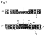
- Fig. 1 shows steps of producing a printed wiring board for use in a metal-plate-inserted ball grid array type semiconductor plastic package in Example 1.
- Fig. 2 shows steps of producing a printed wiring board for use in a metal-plate-inserted ball grid array type semiconductor plastic package in Example 1.
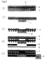
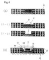
- Fig. 3 shows steps of producing a printed wiring board for use in a metal-core-inserted ball grid array type semiconductor plastic package in Example 2.
- Fig. 4 shows steps of producing a printed wiring board for use in a metal-core-inserted ball grid array type semiconductor plastic package in Example 2.
- Fig. 5 shows steps of producing a semiconductor plastic package using a printed wiring board of the present invention for a metal-core-inserted ball grid array.
- Fig. 6 shows steps of producing a semiconductor plastic package using a printed wiring board of the present invention for a metal-core-inserted ball grid array.
- Fig. 7 shows steps of producing a semiconductor plastic package in Comparative Example 2.
- Fig. 8 shows steps of producing a semiconductor plastic package in Comparative Example 3.
- a shows a metal plate
- b shows a glass fabric base material/thermosetting resin layer
- c shows an elevated portion
- d shows metal protrusions having the form of frustum of a cone each
- f shows a semiconductor chip (which is isolated from its circumferential circuit)
- g shows a prepreg sheet having a hole corresponding to the area of the metal protrusions
- h shows a copper foil
- i shows a double-side copper-clad multilayer laminate
- j shows a metal exposed portion (flat portion) where a semiconductor chip is to be mounted
- k shows a through hole for connecting circuits on front and reverse surfaces
- l shows a semiconductor chip
- m shows a heat-conductive adhesive (silver paste)
- n shows a bonding wire
- o shows an encapsulation resin
- p shows a plating resist
- q shows a solder ball
- r shows a heat-diffusing through hole
- s
- a semiconductor plastic package is produced as follows. A semiconductor chip is fixed on a surface of a metal plate which surface constitutes a cavity, with a heat-conductive adhesive such as a silver paste, the semiconductor chip is connected by wiring bonding, then the semiconductor chip and bonding wires are encapsulated with a resin, and solder balls are melt-connected to a reverse surface.
- a heat-conductive adhesive such as a silver paste
- the semiconductor plastic package produced according to the present invention is excellent in heat conductivity, free of absorption of moisture from its lower surface, is greatly improved in heat resistance after moisture absorption, i.e., causes no popcorn phenomenon, and is also suitable for mass production. There is therefore provided semiconductor plastic packages which are improved in economic performances and have a novel structure. Further, the present invention uses a polyfunctional cyanate ester composition as a thermosetting resin, so that there can be provided semiconductor plastic packages which are excellent in electric insulation after a pressure cooker test and anti-migration properties and have a novel structure.
- a metal plate is placed in a region located as part of the thickness direction of a printed wiring board.
- a region of the metal plate which region is for mounting a semiconductor chip is flat.
- metal protrusions having the form of frustum of a cone each are connected to a copper foil forming a surface on the opposite side.
- the metal plate has a size nearly equivalent to the size of printed wiring board.
- the surface region of the metal plate which surface region is for mounting a semiconductor chip is positioned at a level lower than the level of a circuit conductor including a peripheral bonding pad, and the surface region constitutes a cavity and is an exposed metal surface.
- At least one semiconductor chip is fixed to the above surface region with a heat-conductive adhesive, and the above circuit conductor and the semiconductor chip are connected to each other by wire bonding through the bonding pad.
- protrusions which have the form of frustum of a cone each and are formed of part of the metal plate are in contact with, and connected to, a copper foil forming the opposite surface, and a circuit conductor pad formed for connecting a circuit conductor formed so as to be connected to the above metal protrusions or the package to an outside is connected to at least the signal propagation circuit conductor on the front surface with a through hole conductor.
- at least the semiconductor chip, the wire and the bonding pad are encapsulated with a resin.
- the bonding pad is formed at two levels in the thickness direction, and the semiconductor is connected to the bonding pad by wire bonding.
- the method of producing the printed wiring board of the present invention 1 comprises the following steps.
- the method of producing a printed wiring board according to the present invention 2 comprises
- the method of forming a cavity portion which constitutes a semiconductor-chip-mounting portion in the double-side copper-clad laminate is not critical.
- the cavity portion is formed by removing copper foil on the semiconductor-chip-mounting portion and then cutting off glass fabric base and thermosetting resin composition by a sand blasting method.
- the double-side copper-clad laminate may have circuits formed on front and reverse surfaces thereof in advance of the above cutting by a sand blasting method. In this case, the circuits formed on the front and reverse surfaces are coated with a protective resist before the sand blasting is carried out.
- the plating with a noble metal there may be employed a constitution in which the entire surface is plated with a noble metal and a portion on which the plating is unnecessary is coated with a permanent protective resist.
- the present invention employs a structure in which the through hole is not formed below a region where a semiconductor is mounted, so that no moisture is absorbed through the reverse surface of the semiconductor, so that the possibility of the popcorn phenomenon occurring is remarkably low, and there can be provided a method of producing a semiconductor plastic package having excellent heat diffusibility.
- the method of forming a cavity portion which constitutes a semiconductor-chip-mounting portion in the double-side copper-clad multi-layered board is not critical.
- the cavity portion is formed by cutting off coopper foil, glass fabric base and thermosetting resin composition on the semiconductor-chip-mounting portion by a sand blasting method.
- metal foil, glass fabric base and thermosetting resin composition on the semiconductor-chip-mounting portion and on a region which is to constitute the bonding pad portion of the second level are cut off by a sand blasting method, to expose the bonding pad of the second level.
- the bonding pad of the second level is protected with a protective coating or a protective metal so as not to be cut off, as required, and glass fabric base and thermosetting resin composition is cut off by a sand blasting method, or the like, until the region of the metal plate which region is to constitute the semiconductor-chip-mounting portion is reached and exposed.
- the bonding pad of the first level and a circuit are formed on the front surface, and on the reverse surface, the solder ball pads for connecting the metal foil with which the metal protrusions having the form of frustum of a cone each are in contact to heat-diffusing solder balls and a circuit are formed. At least the semiconductor chip, the wire bonding pads and the solder ball pads are coated with a plating resist, and plating with nickel and gold is carried out, to complete the printed wiring board.
- the method of preparing the metal plate is not critical.
- a metal plate, a glass fabric base impregnated with a thermosetting resin composition and a copper foil are laminated in this order, to obtain a copper-clad laminate, an etching resist is applied onto the entire surface of the laminate, the etching resist present in a region of the exposed metal plate surface which region is to constitute metal protrusions having the form of frustum of a cone each and present on the copper foil on a front surface are retained, the rest of the etching resist is removed, and both sides of the laminate are etched to form an elevated portion in the region which is to constitute the metal protrusions.
- the plating resist is peeled off, and then the entire surface is coated with a plating resist.
- a circuit of the second level bonding pad is formed on the front surface.
- the etching resist is retained in the form of circles having small diameters on the elevated portion of the metal plate and the etching resist is retained so as to form a circuit on the other region. Etching is carried out so as to form a circuit and metal protrusions having the form of frustum of a cone each.
- each protrusion having the form of frustum of a cone has a diameter of 0 to 1 mm
- the bottom of each protrusion has a diameter of 0.5 to 5 mm.
- the double-side metal-clad laminate having the above metal protrusions on one surface and circuits on both the surfaces are surface-treated by a known method as required.
- the surface treatment includes oxidation treatment, fine-roughening treatment and formation of a coating for improving adhesion and insulation.
- a heat-conductive adhesive or a solder may be applied to tops of the above metal protrusions.
- a glass fabric base prepreg sheet having a hole made a little larger than the area of the metal protrusions is placed on the so-treated reverse surface of the metal plate.
- the glass fabric base prepreg sheet has a thickness such that its upper surface is on a level lower than the level of peaks of the metal protrusions after a laminate is formed under heat and pressure.
- a copper foil is placed on the glass fabric base prepreg sheet, and the resultant set is formed into a laminate under heat and pressure preferably in vacuum, such that top edges of the protrusions of the metal plate cut into the copper foil or comes in contact with the copper foil tightly.
- These members are accordingly integrated to give a double-side copper-clad multi-layered board.
- a glass fabric base prepreg sheet having a hole made a little larger than the area of the metal protrusions having the form of frustum of a cone each is placed on the protrusion side of the metal plate, a metal foil is placed on the prepreg sheet, a glass fabric base prepreg sheet is placed on the front surface having a region where a semiconductor chip is to be mounted, and a copper foil is placed on the prepreg.
- the resultant set is formed into a laminate under heat and pressure preferably in vacuum, such that top edges of the protrusions of the metal plate cut into the copper foil or comes in contact with the copper foil tightly.
- a penetration hole for a through hole is made in the above double-side copper-clad multi-layered board with a mechanical drill or a laser, and when the region where a semiconductor chip is to be mounted is formed so as to be isolated from a circumferential metal foil, the penetration hole is made so as to be partly in contact with the metal for using the circumferential metal foil as a circuit, and the penetration hole is placed to form a through hole.
- the penetration hole is made so as not be in contact with the metal, and the entire wall of the penetration hole is plated.
- ball pads are formed in a portion where the top edges of the metal protrusions having the form of frustum of a cone each are in contact with a copper foil forming the outer surface or in a portion other than the above portion.
- a circuit is formed on the entire surface by a known method such that the ball pads are connected to the copper foil on the metal protrusions with the circuit.
- thermosetting resin above a region where a semiconductor chip is to be mounted are cut off by a spot facing method, a sand blasting method or the like until the metal plate located as an inner layer is reached, to expose the metal plate, whereby a cavity type base board is obtained.
- Circuits are formed on the front and reverse surfaces, and at least a bonding pad portion and a solder ball pad portion on the front and reverse surfaces are coated with a plating resist. Nickel and gold plating is carried out, to obtain a printed wiring board.
- the circuits may be formed on the front and reverse surfaces prior to the cutting with a sand blasting method.
- the circuits on the front and reverse surfaces are coated with a protective resist or a protective metal before the sand blasting.
- a noble metal plating there may be employed a constitution in which the entire surface is plated with a noble metal and a portion on which the plating is not necessary is coated with a permanent protective coating.
- metal foil, glass fabric base and thermosetting resin above a region where a semiconductor chip is to be mounted and the wire bonding pad portion of the second level are cut off by spot facing, laser or sand blasting method until the bonding pad of the second level is exposed, and then a remainder on the region where a semiconductor chip is to be mounted is cut off until the metal plate located as an inner layer is reached, to expose the metal plate, whereby a base board having a semiconductor-chip-mounting portion formed in the form of a cavity is produced.
- the bonding pad of the second level is prepared preferably by a sand blasting method in view of accuracy.
- solder balls are melted and connected, whereby a semiconductor plastic package is obtained.
- the solder ball pad portion of the reverse surface is connected to a mother board printed wiring board with the solder balls.
- Heat generated from the semiconductor chip is thermally conducted from the semiconductor-chip-mounting portion to the solder ball pads through the protrusions of the metal plate and diffused into the mother board printed wiring board which is connected to the solder ball pads with the solder balls.
- Side surfaces of the meal plate may have any structure, such as a structure in which they are filled with a thermosetting resin composition or they are exposed. In view of prevention of rust, the side surfaces are preferably filled with a thermosetting resin composition.
- a hole for a through hole for connecting the circuits on the front and reverse surfaces is made nearly in the center of a resin-filled clearance hole or slit of the metal plate so as not to be in contact with the metal plate when the semiconductor-chip-mounting portion of the metal plate is in contact with a circumferential metal plate.
- the wall of the hole is plated to form a metal layer by electroless plating or electric plating, to form a plated through hole.
- the circumferential metal plate can be used as a circuit, so that the through hole is made so as connect the circuit.
- the sand blasting method may be any generally known sand blasting method. Specifically, it includes a dry type air blasting method, a shot blasting method and a wet type wet blasting method.
- a powder used in the above method is selected as required.
- a known powder such as silica sand or glass powder having a size of 20 ⁇ m or less can be used.
- the pressure therefor is not critical, and the sand blasting is carried out generally at 0.1 to 0.5 MPa.
- a noble metal plating is formed at least on the surfaces of the semiconductor-chip-mounting portion, the bonding pad portion and the solder ball pad portion, whereby the printed wiring board is completed.
- a portion where no noble metal plating is required is coated with a plating resist beforehand. Otherwise, after the plating is carried out, a coating is formed on a surface other than the surfaces of the semiconductor-chip-mounting portion, the bonding pad portion and the solder ball pad portion.
- a semiconductor chip is fixed to the flat metal plate as an inner layer of the printed wiring board with a heat-conductive adhesive, the semiconductor chip and the bonding pad of circuit of the printed wiring board are connected by a wire bonding method, and at least the semiconductor chip, the bonding wire and the bonding pad are encapsulated with a known sealing resin.
- the semiconductor chip and the bonding pads of the first and second levels are connected by a wire bonding method.
- Solder balls are connected to the conductor pad for connecting solder balls on the reverse surface opposite to the surface where the semiconductor chip is mounted, whereby P-BGA is obtained.
- the solder balls are brought into contact with a circuit of a mother board printed wiring board and melted by heat to be connected to the circuit.
- a conductor pad formed on the surface of a mother board printed wiring board for connecting solder balls and a conductor pad for solder balls for P-LGA are connected to each other by melting the solder balls.
- the metal plate (also referred to as "metal foil” or “copper foil”) used in the present invention is not specially limited, while the metal plate has a high elastic modulus and high heat conductivity, and the thickness of the metal plate is preferably 100 to 400 ⁇ m, more preferably 5 to 200 ⁇ m.
- the thickness of the metal plate is preferably 100 to 400 ⁇ m, more preferably 5 to 200 ⁇ m.
- preferred is pure copper, oxygen-free copper or an alloy of copper with any one of Fe, Sn, P, Cr, Zr, Zn or the like.
- An alloy plated with copper may be also used.
- a known copper foil is used as such.
- an electrolytic copper foil having a thickness of 3 to 18 ⁇ m is used as a copper foil.
- the height of the metal protrusions having the form of frustum of a cone each is not critical.
- the metal protrusions have a height hither than the level of the surface of the metal plate as a base by 50 to 150 ⁇ m.
- the thickness of an insulation layer such as a prepreg sheet is slightly smaller than the height of the above metal protrusions after a laminate is formed under heat and pressure, and the above thickness is preferably smaller by 5 to 10 ⁇ m.
- a resin is filled among the metal protrusions, among lines of a circuit and in the clearance hole or slit. Top edges of the above metal protrusions are at least in contact with, and connected to, part of a copper foil forming an outer layer.
- the region where the metal protrusions having the form of frustum of a cone each is formed has an area approximately equivalent to the area of a semiconductor chip, and generally, the region has an area of 5 x 20 mm or smaller.
- the ball pads are formed where the copper foil is not in contact with the metal protrusions of the metal plate reverse surface, and the ball pads are connected to the metal foil on the protrusions with a circuit, whereby the adhesion strength between the ball pad portion and the board can be retained and the peel strength (ball shear strength) when a force is laterally exerted on the balls can be retained.
- the resin for the thermosetting resin composition used in the present invention can be selected from generally known thermosetting resins.
- the resin includes an epoxy resin, a polyfunctional cyanate ester resin, a polyfunctional maleimide-cyanate ester resin, a polyfunctional maleimide resin and an unsaturated-group-containing polyphenylene ether resin. These resins may be used alone or in combination. In view of heat resistance, humidity resistance, anti-migration properties and electric properties after moisture absorption, a polyfunctional cyanate ester resin compound is preferred.
- the polyfunctional cyanate ester compound which is a preferred thermosetting resin component in the present invention refers to a compound having a molecule containing at least two cyanato groups.
- Specific examples of the cyanate ester compound include 1,3- or 1,4-dicyanatobenzene, 1,3,5-tricyanotobenzene, 1,3-, 1,4-, 1,6-, 1,8-, 2,6- or 2,7-dicyanatonaphthalene, 1,3,6-tricyanatonaphthalene, 4,4'-dicyanatobiphenyl, bis(4-dicyanatophenyl)methane, 2,2-bis(4-cyanatophenyl)propane, 2,2-bis(3,5-dibromo-4-cyanatophenyl)propane, bis(4-cyanatophenyl)ether, bis (4-cyanatophenyl)thioether, bis(4-cyanotophenyl)sulfone, tris(4-cyanatophenyl)phos
- polyfunctional cyanate ester compounds disclosed in Japanese Patent Publications Nos. 41-1928, 43-18468, 44-4791, 45-11712, 46-41112 and 47-26853 and JP-A-51-63149.
- the above prepolymer can be obtained by polymerizing the above polyfunctional cyanate ester monomer in the presence of a catalyst selected from acids such as mineral acid and Lewis acid, bases such as sodium alcoholate and tertiary amines, or salts such as sodium carbonate.
- the prepolymer partially contains unreacted monomer and has the form of a mixture of a monomer and a prepolymer, and the prepolymer in the above form is also suitably used in the present invention.
- the prepolymer is used in the form a solution thereof in an organic solvent in which it is soluble.
- the epoxy resin can be selected from generally known epoxy resins. Specific examples thereof include a liquid or solid bisphenol A type epoxy resin, a bisphenol F type epoxy resin, a phenol novolak type epoxy resin, a cresol novolak type epoxy resin, an alicyclic epoxy resin; a polyepoxy compound obtained by epoxidizing the double bond of butadiene, pentadiene, vinylcyclohexene or dicyclopentyl ether; a polyol, and a polyglycidyl compound obtained by a reaction between a hydroxyl-group-containing silicone resin and epohalohydrin. These resins may be used alone or in combination.
- the polyimide resin is generally selected from known polyimide resins. Specifically, it is selected from reaction products from polyfunctional maleimides and polyamines, and particularly from, polyimides having terminal triple bonds, disclosed in JP-B-57-005406.
- thermosetting resins may be used alone, while it is preferred to use them in combination as required in view of the balance of properties.
- thermosetting resin composition in the present invention so long as the inherent properties of the composition are not impaired.
- the above additives include monomers having polymerizable double bonds such as unsaturated polyester, prepolymers of these; liquid elastic rubbers having a low molecular weight or elastic rubbers having a high molecular weight such as polybutadiene, epoxidized butadiene, maleated butadiene, a butadiene-acrylonitrile copolymer, polychloroprene, a butadiene-styrene copolymer, polyisprene, butyl rubber, fluorine rubber and natural rubber; polyethylene, polypropylene, polybutene, poly-4-methylpentene, polystyrene, AS resin, ABS resin, MBS resin, styrene-isoprene rubber, a polyethylene-propylene copolymer, a 4-fluoroethylene-6-fluoroethylene copolymer; high-mole
- additives are used as required. Further, various known additives such as an inorganic or organic filler, a dye, a pigment, a thickener, a lubricant, an anti-foamer, a dispersing agent, a leveling agent, a photo-sensitizer, a flame retardant, a brightener, a polymerization inhibitor and a thixotropic agent may be used alone or in combination as required. A curing agent or a catalyst is incorporated into a compound having a reactive group as required.
- thermosetting resin composition used in the present invention undergoes curing itself under heat.
- a known heat-curing catalyst is incorporated into the thermosetting resin.
- the amount of the catalyst per 100 parts by weight of the thermosetting resin is 0.005 to 10 parts by weight, preferably 0.01 to 5 parts by weight.
- the glass fabric base material used as a reinforcement for the prepreg is selected from generally known woven and non-woven fabrics, while a woven fabric is preferred in view of a strength. Specifically, it is selected from a know glass fiber fabric of E glass, S glass, D glass or the like. These fabrics may be a fabric obtained by intertwining different glass fibers. Further, an organic base material may be used, and it is selected from a generally known woven or non-woven fabric of a liquid crystal polymer fiber or an wholly aromatic polyamide fiber.
- the diameter of the clearance hole or the width of the slit made in the metal plate is a little larger than the diameter of the through hole for conduction between the front and reverse surfaces.
- the wall of the through hole is preferably insulated with the thermosetting resin composition so as to have a distance of at least 50 ⁇ m from the wall of the clearance hole or the slit made in the metal plate.
- the diameter of the through hole for conduction between the front and reverse surfaces is preferably 50 to 300 ⁇ m.
- the base material is impregnated with the thermosetting resin composition, and the thermosetting resin composition is dried to obtain a semi-cured laminating material.
- a semi-cured resin layer of the prepreg is formed generally at 100 to 180°C, and the time period is 5 to 60 minutes. These conditions are properly selected depending upon an intended flow degree.
- the method of preparing the metal plate and the method of producing the printed wiring board having the metal plate, for a semiconductor plastic package are not specially limited.
- the above metal plate and the printed wiring board are produced, for example, by the following method (Figs. 1 and 2).
- the semiconductor-chip-mounting portion which is present in the central area and has the metal protrusions on the reverse surface has a form (3-2; f) in which it is isolated from metal foil having a circumferential circuit formed thereon.
- the method of preparing the metal plate and the method of producing the printed wiring board having the metal plate, for a semiconductor plastic package are modified.
- the above metal plate and the printed wiring board are produced, for example, by the following method (Figs. 3 and 4).
- a semiconductor chip (l) is fixed on the semiconductor-chip-mounting portion (j) formed of the exposed surface of the metal plate with a heat-conductive adhesive, connected with a bonding wire (n) and encapsulated with a resin (o), and solder balls (q) are bonded and fixed to the solder ball pads by melting them, to give a semiconductor plastic package.
- a method of producing a printed wiring board having a novel structure for a semiconductor plastic package which is excellent in strength of adhesion to solder balls, which is free of moisture absorption from the lower surface of a semiconductor chip, which is greatly improved in heat resistance after moisture absorption, i.e., does not cause a popcorn phenomenon, and which is suitable for mass production and improved in economic performances.
- a method of producing a printed wiring board for a semiconductor plastic package which is excellent in insulation properties after pressure cooker treatment and anti-migration properties.
- a catalyst 0.4 part of zinc octylate was added, dissolved and mixed.
- an inorganic filler (trade name: Calcined Talc, supplied by Nippon Talc K.K.), and these materials were homogeneously stirred and mixed to prepare a varnish A.
- a 50 ⁇ m thick glass woven fabric was impregnated with the above varnish, and the impregnated glass woven fabric was dried to prepare a semi-cured prepreg (prepreg B) having a gelation time of 50 seconds (at 170°C) and having a resin flow of 8 mm at 170°C at 20 kgf/cm 2 for 5 minutes.
- the prepreg B had an insulation layer thickness of 88 ⁇ m.
- a 18 ⁇ m thick electrolytic copper foil was placed on one surface of a sheet of the above prepreg B, a 105 ⁇ m thick electrolytic copper foil was placed on the other surface, and the resultant set was formed into a laminate at 200°C at 20 kgf/cm 2 for 2 hours, to give a double-side copper-clad laminate.
- the entire surface of the laminate was coated with an etching resist having a thickness of 25 ⁇ m, etching resist on the entire surface of the 18 ⁇ m thick copper foil was retained, and on the 105 ⁇ m thick copper foil side, etching resist was retained so as to cover an area where an elevated portion was to be formed.
- Etching was carried out to give a double-side copper clad-laminate having an elevated portion (c) on one surface (Fig. 1-(2)).
- the retained resist was removed, the entire surface was coated with a liquid etching resist having a thickness of 25 ⁇ m, 400 resist circles having a diameter of 250 ⁇ m were retained on the elevated portion opposite to a 15 x 15 mm square area which was to be located in a central area of a 50 x 50 mm package area and which was to constitute a semiconductor-chip-mounting portion, resist was retained in a circumferential area around the elevated portion, and etching was carried out to form 400 protrusions (d) having the form of frustum of a cone each and a circuit (e) in an circumferential area (Fig.
- Each protrusion had a height of 85 ⁇ m from the base copper foil surface, a bottom side diameter of 507 ⁇ m and a top side diameter of 108 ⁇ m.
- a copper foil portion which was to constitute a semiconductor-chip-mounting portion having the protrusions on its reverse surface had a structure (f) where it was isolated from a copper foil for forming a circumferential circuit.
- the copper foil surface of the laminate was oxidation-treated to form a black copper oxide, and then one sheet of the above prepreg B (g) was placed on the reverse surface.
- the above prepreg B sheet had a hole which corresponded to an area of the metal protrusions and had an area little larger the area of the metal protrusions.
- a 18 ⁇ m thick electrolytic copper foil (h) was placed on the prepreg B sheet, and the resultant set was formed into a laminate and integrated, to give a double-side copper-clad multi-layered board (i).
- Through holes having a diameter of 0.25 ⁇ m each were made with a mechanical drill, and after desmear treatment, the entire surface was copper-plated to form a 20 ⁇ m thick copper layer by electroless plating and electrolytic plating, whereby through hole conductors (k) were formed.
- Copper foil on the semiconductor-chip-mounting portion was removed by etching, and glass fabric base material and thermosetting resin composition were cut off from the front surface by a sand blasting method until a metal surface was reached.
- Sand used with the blasting method was removed through a soft etching step, and then, circuits were formed on the front and reverse surfaces. Solder ball pads on the reverse surface were formed so as not to overlap with the peaks of the metal protrusions.
- a plating resist (p) was formed on a portion which was not any of the semiconductor-chip-mounting portion, the wire bonding portion and ball pad portion on the reverse surface, and nickel plating and gold plating were carried out, to complete a printed wiring board.
- a semiconductor chip having a size of 13 x 13 mm was fixed to the flat inner layer metal plate portion which was the semiconductor chip mounting portion on the front surface, with a silver paste (m), and wire bonding was carried out. Then, the semiconductor chip (l), a wire (n) and the bonding pads were encapsulated with a resin, and solder balls (q) were bonded to the reverse surfaces, to complete a semiconductor plastic package.
- the semiconductor plastic package was connected to an epoxy resin mother board printed wiring board by melting the solder balls. Tables 1 and 2 show evaluation results.
- Example 2 Two sheets of the prepreg B obtained in Example 1 were used as a laminate. A 12 ⁇ m thick electrolytic copper foil was placed on one surface of the laminate, and 12 ⁇ m thick electrolytic copper foil was also placed on the other surface. The resultant set was formed into a laminate at 200°C at 20 kgf/cm 2 under a vacuum of 30 mmHg or less, to give a double-side copper-clad laminate. Through holes having a diameter of 0.25 mm were made in predetermined positions with a drill, and after desmear treatment, copper plating was carried out. Circuits were formed on the front and reverse surfaces of the laminate by a known method, followed by coating with a plating resist and plating with nickel and gold.
- the resultant board had heat-diffusing through holes in a region where a semiconductor chip was to be mounted.
- a semiconductor chip was bonded to the region with a silver paste, followed by wire bonding and also followed by encapsulation with an epoxy sealing compound and connection with solder balls in the same manner as in Example 1.
- the resultant package was bonded to a mother board. Tables 1 and 2 show evaluation results.
- a glass woven fabric having a thickness of 100 ⁇ m was impregnated with the above mixture, and the impregnated glass woven fabric was dried to obtain a no-flow prepreg (prepreg C) having a gelation time of 10 seconds and a resin flow of 98 ⁇ m and a high-flow prepreg (prepreg D) having a gelation time of 150 seconds and a resin flow of 18 mm.
- prepreg C no-flow prepreg
- prepreg D high-flow prepreg
- Two sheets of the prepreg D were used, and a double-side copper-clad laminate was prepared by laminate-formation at 190°C at 20 kgf/cm 2 under a vacuum of 30 mmHg or less for 2 hours.
- a printed wiring board was prepared in the same manner as in Comparative Example 1, a hole was made in a portion for a semiconductor-chip-mounting portion with a spot facing machine, and a copper plate having a thickness 200 ⁇ m and a sheet of the above no-flow prepreg C having a central hole were laminated thereon.
- the resultant set was integrated under heat and pressure, to obtain a radiator-possessing printed wiring board.
- the so-obtained printed wiring board underwent distortion.
- a semiconductor chip was fixed directly to the radiator with a silver paste, followed by wire bonding and encapsulation with a liquid epoxy resin (Fig. 8). The resultant package was bonded to a mother board printed wiring board. Tables 1 and 2 show evaluation results.
- Example Comparative Example 1 1 2 Ball shear strength (kgf) 1.6 - - Heat resistance A after moisture absorption Normal state No failure No failure No failure 24 hours No failure No failure 48 hours No failure No failure No failure 72 hours No failure No failure No failure 96 hours No failure No failure No failure Partly peeled 120 hours No failure Partly peeled Partly peeled 144 hours No failure Partly peeled Partly peeled 168 hours No failure Partly peeled Partly peeled Heat resistance B after moisture absorption Normal state No failure No failure No failure 24 hours No failure Partly peeled Partly peeled 48 hours No failure Largely peeled Largely peeled 72 hours No failure Wire broken Wire broken 96 hours No failure Wire broken Wire broken 120 hours No failure Wire broken Wire broken 144 hours No failure - - 168 hours No failure - - Example Comparative Example 1 1 2 Insulation resistance value ( ⁇ ) after pressure cooker treatment Normal state 5 x 10 14 1 x 10 14 6 x 10 14 200 hours 5 x 10 12 4 x 10
- a solder ball was bonded to a ball pad having a diameter of 0.65 mm, and laterally pressed to be peeled off. The ball was measured for a strength when it was peeled off.
- a printed wiring board was treated at 30°C at 60 %RH for predetermined period of time according to JEDEC STANDARD TEST METHOD A113-A LEVEL 3 and then subjected to 3 cycles of a 220°C reflow solder test, and the board was studied for any failure by observation of its cross section and electric checking.
- a printed wiring board was treated at 85°C at 60 %RH for predetermined period of time (maximum 168 hours) according to JEDEC STANDARD TEST METHOD A113-A LEVEL 2 and then subjected to 3 cycles of a 220°C reflow solder test, and the board was studied for any failure by observation of its cross section and electric checking.
- a package was bonded to an identical mother board printed wiring board with solder balls and continuously used for 1,000 hours, and the package was measured for a temperature.
- a 50 ⁇ m thick glass woven fabric was impregnated with the same varnish A as that obtained in Example 1, and the impregnated glass woven fabric was dried so as to obtain a semi-cured prepreg E having a gelation time of 50 seconds (at 170°C) and a resin flow of 12 mm at 170°C at 20 kgf/cm 2 for 5 minutes.
- the prepreg E had an insulation layer thickness of 137 ⁇ m.
- a 35 ⁇ m thick electrolytic copper foil was placed on one surface of the above prepreg E, a 165 ⁇ m thick electrolytic copper foil was also placed on the other surface, and the resultant set was formed into a laminate at 200°C at 20 kgf/cm 2 for 2 hours, to give a double-side copper-clad laminate.
- the entire surface of the laminate was coated with a 25 ⁇ m thick etching resist, etching resist was retained on the entire 35 ⁇ m thick copper foil side, and on the 165 ⁇ m thick copper foil side, etching resist was retained so as to cover an area where protrusions having the form of frustum of a cone were to be formed.
- Etching was carried out from both the surfaces, to give a double-side copper-clad laminate (Fig.3-(2)) having an elevated portion (c) on one surface.
- the retained resist was removed, and the entire surface was again coated with a liquid etching resist to form a 25 ⁇ m thick etching resist layer.
- 225 resist circles having a diameter of 250 ⁇ m were retained on the elevated portion opposite to a 15 x 15 mm square area which was to be located in a central area of a 50 x 50 mm package area and which was to constitute a semiconductor-chip-mounting portion, and resist was retained in a circumferential area around the elevated portion.
- protrusions On the front surface, resist was retained for forming bonding pads of a second level and a surface-layer circuit, and etching was carried out from both sides to form 225 protrusions (d) having the form of frustum of a cone each and circuits (e) in circumferential areas on the front and reverse surfaces (Fig. 1-(3)). Each protrusion had a height of 130 ⁇ m, a bottom portion diameter of 612 ⁇ m and a top portion diameter of 180 ⁇ m.
- a copper foil portion which was to constitute a semiconductor-chip-mounting portion having the protrusions on its reverse surface had a structure (f) where it was isolated from a copper foil for forming the circumferential circuit.
- the copper foil surfaces of the laminate were oxidation-treated to form a black copper oxide, and then one sheet of the above prepreg E (s) was placed on the front surface side.
- a sheet of the above prepreg E sheet was also placed on the reverse surface. The latter sheet had a hole which corresponded to an area of the metal protrusions and had an area little larger the area of the metal protrusions.
- a 18 ⁇ m thick electrolytic copper foil (h) was placed on one of the sheets of the prepreg B, a 18 ⁇ m thick electrolytic copper foil (h) was placed on the other of the sheets of the prepreg E, and the resultant set was similarly formed into a laminate and integrated, to give a double-side copper-clad multi-layered board (i).
- Through holes having a diameter of 0.25 ⁇ m each were made with a mechanical drill, and after desmear treatment, the entire surface was copper-plated to form a 20 ⁇ m thick copper layer by electroless plating and electrolytic plating, whereby through hole conductors (k) were formed.
- Circuits were formed on the front and reverse surfaces, and at the same time, copper foil on areas which were to constitute the semiconductor-chip-mounting portion and bonding pads of a second level was removed by etching, a surface which was not on a region to constitute the semiconductor-chip-mounting portion or the bonding pads of the second level was coated with a resist, and glass fabric base material and thermosetting resin composition were cut off from the front surface by a sand blasting method until a portion which was to constitute the bonding pads of the second level was reached.
- any surface other than the region which was to constitute the semiconductor-chip-mounting portion was coated with a protective resist, glass fabric base material and thermosetting resin composition (v) were cut off by a sand blasting method until a metal core was reached, and the resist was peeled off. Then, sand used with the sand blasting method was removed through a soft etching step. Solder ball pads on the reverse surface were formed so as not to overlap with the peaks of the metal protrusions, but were formed so as to be connected to the copper foil on the protrusions.
- a plating resist (p) was formed on a portion which was not any of the semiconductor-chip-mounting portion, the wire bonding portion and a ball pad portion on the reverse surface, and nickel plating and gold plating were carried out, to complete a printed wiring board.
- a semiconductor chip having a size of 13 x 13 mm was fixed to the flat inner-layer metal core which was the semiconductor chip mounting portion on the front surface, with a silver paste (m), and wire bonding on the first and second levels was carried out. Then, the semiconductor chip (l), wires (n) and the bonding pads (w) were encapsulated with a silica-containing sealing liquid resin (o), and solder balls (q) were bonded to the reverse surfaces, to complete a semiconductor plastic package.
- the semiconductor plastic package was connected to an epoxy resin mother board printed wiring board by melting the solder balls. Tables 3 and 4 show evaluation results.
- a semiconductor plastic package was prepared in the same manner as in Example 2 except that solder ball pads were formed on protrusions having the form of frustum of a cone each. Tables 3 and 4 show evaluation results.
- Example 2 Two sheets of the prepreg E obtained in Example 2 were used as a laminate. A 12 ⁇ m thick electrolytic copper foil was placed on one surface of the laminate, and a 12 ⁇ m thick electrolytic copper foil was placed on the other surface, and the resultant set was formed into a laminate at 200°C at 20 kgf/cm 2 under a vacuum of 30 mmHg or less, to give a double-side copper-clad laminate. Through holes having a diameter of 0.25 mm were made in predetermined positions, and after desmear treatment, copper plating was carried out. Circuits were formed on the front and reverse surfaces by a known method, followed by coating with a plating resist, nickel plating and gold plating.
- the resultant board had heat-diffusing through holes in a region where a semiconductor chip was to be mounted.
- a semiconductor chip was bonded to the region with a silver paste, followed by wire bonding and encapsulation with an epoxy sealing compound in the same manner as in Example 2. Solder balls were connected (Fig. 8). The so-obtained package was similarly bonded to a mother board. Tables 3 and 4 show evaluation results.
- Example Comparative Example 2 3 4 Ball shear strength (kgf) 1.4 0.9 - Heat resistance A after moisture absorption Normal state No failure - No failure 24 hours No failure - No failure 48 hours No failure - No failure 72 hours No failure - No failure 96 hours No failure - No failure 120 hours No failure - Partly peeled 144 hours No failure - Partly peeled 168 hours No failure - Partly peeled Heat resistance B after moisture absorption Normal state No failure - No failure 24 hours No failure - Partly peeled 48 hours No failure - Largely peeled 72 hours No failure - Wire broken 96 hours No failure - Wire broken 120 hours No failure - Wire broken 144 hours No failure - - 168 hours No failure - - Example Comparative Example 2 3 4 Insulation resistance value ( ⁇ ) after pressure cooker treatment Normal state 5 x 10 14 - 6 x 10 14 200 hours 7 x 10 12 - 5 x 10 12 500 hours 8 x 10 11 - 4 x 10 11 700 hours 3 x 10 10
- Varnish A was prepared in the same manner as in Example 1.
- a 50 ⁇ m thick glass woven fabric was impregnated with the varnish A, and the impregnated glass woven fabric was dried so as to attain a gelation time of 50 seconds (at 170°C) and a resin flow of 10 mm at 170°C at 20 kgf/cm 2 for 5 minutes, whereby a semi-cured prepreg F ving an insulation layer thickness of 75 ⁇ m was obtained.
- etching resist in an area where a clearance hole having a diameter of 0.6 mm was to be made was removed, and etching was carried out from both sides to form 400 protrusions having the form of frustum of a cone each on the reverse surface and a clearance hole in a circumferential area (Fig. 5 (1), (2-1)).
- Each protrusion had a height of 153 ⁇ m, a bottom portion diameter of 645 ⁇ m and a top portion diameter of 110 ⁇ m.
- a 18 ⁇ m thick electrolytic copper foil was placed on one surface of a sheet of the above prepreg F, a 18 ⁇ m thick electrolytic copper foil was also placed on the other surface, and the resultant set was formed in a laminate at 200°C at 20 kgf/cm 2 for 2 hours, to obtain a double-side copper-clad laminate (i). Bonding pads of a second level and other circuit were formed on one surface of the laminate, and the laminate was oxidation-treated to form a black copper oxide. The laminate was placed on the front surface of the above metal plate such that the circuit side faced inward. Two sheets of the above prepreg E (g) were placed on the reverse surface of the metal plate.
- a metal protective sheet (z) was covered on the semiconductor-chip-mounting portion, glass fabric base material and thermosetting resin composition were again cut off by a sand blasting method until a metal core was reached. Then, sand used with the sand blasting method was removed through a soft etching step, and circuits were formed on the front and reverse surfaces. Solder ball pads ( ⁇ ) on the reverse surface were formed so as not to overlap with the peaks of the metal protrusions. A plating resist was formed on a portion which was not any of the semiconductor-chip-mounting portion, the wire bonding portion and a ball pad portion on the reverse surface, and nickel plating and gold plating were carried out, to complete a printed wiring board.
- a semiconductor chip (l) having a size of 13 x 13 mm was fixed to the flat inner-layer metal core which was the semiconductor chip mounting portion on the front surface, with a silver paste (r), and the semiconductor chip was connected to the bonding pads of the first and second levels by wire bonding. Then, the semiconductor chip, wires and the bonding pads were encapsulated with a silica-containing sealing liquid resin (o), and solder balls (q) were bonded to the reverse surfaces, to complete a semiconductor plastic package.
- the semiconductor plastic package was connected to an epoxy resin mother board printed wiring board by melting the solder balls. Tables 5 and 6 show evaluation results.
- Example 3 Ball shear strength (kgf) 1.6 Heat resistance A after moisture absorption Normal state No failure 24 hours No failure 48 hours No failure 72 hours No failure 96 hours No failure 120 hours No failure 144 hours No failure 168 hours No failure Heat resistance B after moisture absorption Normal state No failure 24 hours No failure 48 hours No failure 72 hours No failure 96 hours No failure 120 hours No failure 144 hours No failure 168 hours No failure
Landscapes
- Engineering & Computer Science (AREA)
- Microelectronics & Electronic Packaging (AREA)
- Physics & Mathematics (AREA)
- Condensed Matter Physics & Semiconductors (AREA)
- General Physics & Mathematics (AREA)
- Computer Hardware Design (AREA)
- Power Engineering (AREA)
- Ceramic Engineering (AREA)
- Manufacturing & Machinery (AREA)
- Production Of Multi-Layered Print Wiring Board (AREA)
- Insulated Metal Substrates For Printed Circuits (AREA)
Applications Claiming Priority (6)
| Application Number | Priority Date | Filing Date | Title |
|---|---|---|---|
| JP12505599A JP2000315750A (ja) | 1999-04-30 | 1999-04-30 | 熱放散性に優れたボールグリッドアレイ型プリント配線板の製造方法 |
| JP12505199 | 1999-04-30 | ||
| JP12505199A JP2000315749A (ja) | 1999-04-30 | 1999-04-30 | 金属芯入りボールグリッドアレイ型半導体プラスチックパッケージ用プリント配線板 |
| JP12505599 | 1999-04-30 | ||
| JP17454999 | 1999-06-21 | ||
| JP17454999A JP2001007533A (ja) | 1999-06-21 | 1999-06-21 | 放熱性に優れたボールグリッドアレイ型プリント配線板の製造方法 |
Publications (2)
| Publication Number | Publication Date |
|---|---|
| EP1049151A2 true EP1049151A2 (fr) | 2000-11-02 |
| EP1049151A3 EP1049151A3 (fr) | 2002-10-23 |
Family
ID=27315036
Family Applications (1)
| Application Number | Title | Priority Date | Filing Date |
|---|---|---|---|
| EP00303592A Withdrawn EP1049151A3 (fr) | 1999-04-30 | 2000-04-28 | Méthode de production d'un circuit imprimé du type ball grid array ayant une excellente diffusion thermique et son procédé de fabrication |
Country Status (2)
| Country | Link |
|---|---|
| US (1) | US6396143B1 (fr) |
| EP (1) | EP1049151A3 (fr) |
Cited By (3)
| Publication number | Priority date | Publication date | Assignee | Title |
|---|---|---|---|---|
| CN102256452A (zh) * | 2010-04-02 | 2011-11-23 | 株式会社电装 | 具有内置半导体芯片的电路板以及制造该电路板的方法 |
| CN107037350A (zh) * | 2015-09-23 | 2017-08-11 | 格罗方德半导体公司 | 具有监控链及测试导线的集成电路测试结构 |
| CN110049626A (zh) * | 2019-04-17 | 2019-07-23 | 深圳市景旺电子股份有限公司 | 一种pcb板分类方法 |
Families Citing this family (27)
| Publication number | Priority date | Publication date | Assignee | Title |
|---|---|---|---|---|
| JP3398721B2 (ja) * | 1999-05-20 | 2003-04-21 | アムコー テクノロジー コリア インコーポレーティド | 半導体パッケージ及びその製造方法 |
| US6577004B1 (en) * | 2000-08-31 | 2003-06-10 | Micron Technology, Inc. | Solder ball landpad design to improve laminate performance |
| US6775906B1 (en) * | 2000-10-20 | 2004-08-17 | Silverbrook Research Pty Ltd | Method of manufacturing an integrated circuit carrier |
| JP3926141B2 (ja) * | 2000-12-27 | 2007-06-06 | 日本特殊陶業株式会社 | 配線基板 |
| US6586826B1 (en) * | 2001-06-13 | 2003-07-01 | Amkor Technology, Inc. | Integrated circuit package having posts for connection to other packages and substrates |
| US7015072B2 (en) | 2001-07-11 | 2006-03-21 | Asat Limited | Method of manufacturing an enhanced thermal dissipation integrated circuit package |
| US6734552B2 (en) * | 2001-07-11 | 2004-05-11 | Asat Limited | Enhanced thermal dissipation integrated circuit package |
| JP2003046034A (ja) * | 2001-07-31 | 2003-02-14 | Nec Kagobutsu Device Kk | 樹脂封止型半導体装置 |
| AU2002332557A1 (en) * | 2001-08-15 | 2003-03-03 | Asat Limited | Encapsulated integrated circuit package and method of manufacturing an integrated circuit package |
| US6790710B2 (en) * | 2002-01-31 | 2004-09-14 | Asat Limited | Method of manufacturing an integrated circuit package |
| US20040173894A1 (en) * | 2001-09-27 | 2004-09-09 | Amkor Technology, Inc. | Integrated circuit package including interconnection posts for multiple electrical connections |
| US20030178719A1 (en) * | 2002-03-22 | 2003-09-25 | Combs Edward G. | Enhanced thermal dissipation integrated circuit package and method of manufacturing enhanced thermal dissipation integrated circuit package |
| US6940154B2 (en) * | 2002-06-24 | 2005-09-06 | Asat Limited | Integrated circuit package and method of manufacturing the integrated circuit package |
| JP3920195B2 (ja) * | 2002-11-11 | 2007-05-30 | 新光電気工業株式会社 | 電子部品実装構造及びその製造方法 |
| TWI321342B (en) * | 2004-11-05 | 2010-03-01 | Altus Technology Inc | An integrate circuit chip encapsulation and the method of manufacturing it |
| KR100688857B1 (ko) * | 2004-12-17 | 2007-03-02 | 삼성전기주식회사 | 윈도우를 구비한 볼 그리드 어레이 기판 및 그 제조방법 |
| US9466545B1 (en) | 2007-02-21 | 2016-10-11 | Amkor Technology, Inc. | Semiconductor package in package |
| US7697305B2 (en) * | 2007-04-27 | 2010-04-13 | Hewlett-Packard Development Company, L.P. | Apparatus and method for enhancing conductivity |
| JP5543084B2 (ja) * | 2008-06-24 | 2014-07-09 | ピーエスフォー ルクスコ エスエイアールエル | 半導体装置の製造方法 |
| US7989950B2 (en) * | 2008-08-14 | 2011-08-02 | Stats Chippac Ltd. | Integrated circuit packaging system having a cavity |
| TWI420634B (zh) * | 2011-02-24 | 2013-12-21 | Unimicron Technology Corp | 封裝結構及其製法 |
| TW201241969A (en) * | 2011-04-08 | 2012-10-16 | Unimicron Technology Corp | Method for fabricating heat dissipation substrate |
| KR101920106B1 (ko) * | 2012-01-31 | 2018-11-19 | 미츠비시 가스 가가쿠 가부시키가이샤 | 프린트 배선판 재료용 수지 조성물, 그리고 그것을 사용한 프리프레그, 수지 시트, 금속박 피복 적층판 및 프린트 배선판 |
| TWI554174B (zh) * | 2014-11-04 | 2016-10-11 | 上海兆芯集成電路有限公司 | 線路基板和半導體封裝結構 |
| JP6606331B2 (ja) * | 2015-02-16 | 2019-11-13 | ローム株式会社 | 電子装置 |
| US10361149B2 (en) * | 2016-08-10 | 2019-07-23 | Qualcomm Incorporated | Land grid array (LGA) packaging of passive-on-glass (POG) structure |
| CN116939950A (zh) * | 2022-04-08 | 2023-10-24 | Dsbj私人有限公司 | 在内部铜焊盘上设有阻焊层的电路板 |
Citations (6)
| Publication number | Priority date | Publication date | Assignee | Title |
|---|---|---|---|---|
| US3994949A (en) * | 1974-09-26 | 1976-11-30 | Bayer Aktiengesellschaft | Production of aromatic cyanic acid esters |
| US5113315A (en) * | 1990-08-07 | 1992-05-12 | Cirqon Technologies Corporation | Heat-conductive metal ceramic composite material panel system for improved heat dissipation |
| US5397917A (en) * | 1993-04-26 | 1995-03-14 | Motorola, Inc. | Semiconductor package capable of spreading heat |
| US5642261A (en) * | 1993-12-20 | 1997-06-24 | Sgs-Thomson Microelectronics, Inc. | Ball-grid-array integrated circuit package with solder-connected thermal conductor |
| WO1998015980A1 (fr) * | 1996-10-10 | 1998-04-16 | Samsung Electronics Co., Ltd. | Circuit integre hybride et de grande puissance |
| US5814883A (en) * | 1995-10-04 | 1998-09-29 | Mitsubishi Denki Kabushiki Kaisha | Packaged semiconductor chip |
Family Cites Families (4)
| Publication number | Priority date | Publication date | Assignee | Title |
|---|---|---|---|---|
| US6097089A (en) * | 1998-01-28 | 2000-08-01 | Mitsubishi Gas Chemical Company, Inc. | Semiconductor plastic package, metal plate for said package, and method of producing copper-clad board for said package |
| JPH10112259A (ja) * | 1996-10-09 | 1998-04-28 | Dainippon Printing Co Ltd | 厚膜パターン形成方法 |
| JP3836244B2 (ja) * | 1997-03-18 | 2006-10-25 | 住友ベークライト株式会社 | 樹脂封止型半導体装置 |
| JP3123482B2 (ja) * | 1997-10-08 | 2001-01-09 | 日本電気株式会社 | 低熱抵抗型半導体パッケージ、および低熱抵抗型半導体パッケージの製造方法 |
-
2000
- 2000-04-25 US US09/557,974 patent/US6396143B1/en not_active Expired - Fee Related
- 2000-04-28 EP EP00303592A patent/EP1049151A3/fr not_active Withdrawn
Patent Citations (6)
| Publication number | Priority date | Publication date | Assignee | Title |
|---|---|---|---|---|
| US3994949A (en) * | 1974-09-26 | 1976-11-30 | Bayer Aktiengesellschaft | Production of aromatic cyanic acid esters |
| US5113315A (en) * | 1990-08-07 | 1992-05-12 | Cirqon Technologies Corporation | Heat-conductive metal ceramic composite material panel system for improved heat dissipation |
| US5397917A (en) * | 1993-04-26 | 1995-03-14 | Motorola, Inc. | Semiconductor package capable of spreading heat |
| US5642261A (en) * | 1993-12-20 | 1997-06-24 | Sgs-Thomson Microelectronics, Inc. | Ball-grid-array integrated circuit package with solder-connected thermal conductor |
| US5814883A (en) * | 1995-10-04 | 1998-09-29 | Mitsubishi Denki Kabushiki Kaisha | Packaged semiconductor chip |
| WO1998015980A1 (fr) * | 1996-10-10 | 1998-04-16 | Samsung Electronics Co., Ltd. | Circuit integre hybride et de grande puissance |
Non-Patent Citations (1)
| Title |
|---|
| PATENT ABSTRACTS OF JAPAN vol. 1998, no. 09, 31 July 1998 (1998-07-31) -& JP 10 112259 A (DAINIPPON PRINTING CO LTD), 28 April 1998 (1998-04-28) * |
Cited By (5)
| Publication number | Priority date | Publication date | Assignee | Title |
|---|---|---|---|---|
| CN102256452A (zh) * | 2010-04-02 | 2011-11-23 | 株式会社电装 | 具有内置半导体芯片的电路板以及制造该电路板的方法 |
| CN102256452B (zh) * | 2010-04-02 | 2014-01-29 | 株式会社电装 | 具有内置半导体芯片的电路板以及制造该电路板的方法 |
| CN107037350A (zh) * | 2015-09-23 | 2017-08-11 | 格罗方德半导体公司 | 具有监控链及测试导线的集成电路测试结构 |
| CN107037350B (zh) * | 2015-09-23 | 2019-10-01 | 格罗方德半导体公司 | 具有监控链及测试导线的集成电路测试结构 |
| CN110049626A (zh) * | 2019-04-17 | 2019-07-23 | 深圳市景旺电子股份有限公司 | 一种pcb板分类方法 |
Also Published As
| Publication number | Publication date |
|---|---|
| US6396143B1 (en) | 2002-05-28 |
| EP1049151A3 (fr) | 2002-10-23 |
Similar Documents
| Publication | Publication Date | Title |
|---|---|---|
| US6396143B1 (en) | Ball grid array type printed wiring board having exellent heat diffusibility and printed wiring board | |
| US6097089A (en) | Semiconductor plastic package, metal plate for said package, and method of producing copper-clad board for said package | |
| US6350952B1 (en) | Semiconductor package including heat diffusion portion | |
| US6720651B2 (en) | Semiconductor plastic package and process for the production thereof | |
| JPH11176973A (ja) | 半導体プラスチックパッケージ | |
| JP2000150714A (ja) | 半導体プラスチックパッケージ用プリント配線板 | |
| JP2001007533A (ja) | 放熱性に優れたボールグリッドアレイ型プリント配線板の製造方法 | |
| JPH11214572A (ja) | 金属芯入り両面金属箔張多層板の製造方法 | |
| JP2000260900A (ja) | 半導体プラスチックパッケージ用サブストレート | |
| JP2000150715A (ja) | 金属板入りプリント配線板用銅張板の製造方法 | |
| JP2000260901A (ja) | 金属芯入半導体プラスチックパッケージ用多層プリント配線板 | |
| JPH11238827A (ja) | 金属芯の製造方法 | |
| JP3852510B2 (ja) | 半導体プラスチックパッケージ | |
| JP2000315749A (ja) | 金属芯入りボールグリッドアレイ型半導体プラスチックパッケージ用プリント配線板 | |
| JP2000315750A (ja) | 熱放散性に優れたボールグリッドアレイ型プリント配線板の製造方法 | |
| JPH11195745A (ja) | マルチチッププラスチックパッケージ | |
| JP2000323836A (ja) | 金属芯入りプリント配線板用金属芯の製造方法 | |
| JPH11220061A (ja) | キャビティ型半導体プラスチックパッケージ | |
| JP2000077567A (ja) | プリント配線板の製造方法 | |
| JP2000124342A (ja) | 金属板入りプリント配線板の製造方法 | |
| JPH11220066A (ja) | 半導体プラスチックパッケージ用金属芯入り両面金属箔張積層板の製造方法 | |
| JP2000286361A (ja) | フリップチップ搭載用多層プリント配線板 | |
| JPH11345907A (ja) | 金属芯入りプリント配線板用金属芯の製造方法 | |
| JPH11214563A (ja) | 半導体プラスチックパッケージ | |
| JPH11220064A (ja) | 小型半導体プラスチックパッケージ |
Legal Events
| Date | Code | Title | Description |
|---|---|---|---|
| PUAI | Public reference made under article 153(3) epc to a published international application that has entered the european phase |
Free format text: ORIGINAL CODE: 0009012 |
|
| AK | Designated contracting states |
Kind code of ref document: A2 Designated state(s): AT BE CH CY DE DK ES FI FR GB GR IE IT LI LU MC NL PT SE |
|
| AX | Request for extension of the european patent |
Free format text: AL;LT;LV;MK;RO;SI |
|
| PUAL | Search report despatched |
Free format text: ORIGINAL CODE: 0009013 |
|
| AK | Designated contracting states |
Kind code of ref document: A3 Designated state(s): AT BE CH CY DE DK ES FI FR GB GR IE IT LI LU MC NL PT SE |
|
| AX | Request for extension of the european patent |
Free format text: AL;LT;LV;MK;RO;SI |
|
| RIC1 | Information provided on ipc code assigned before grant |
Free format text: 7H 01L 21/48 A, 7H 01L 23/36 B, 7H 01L 23/498 B, 7H 01L 23/367 B, 7H 05K 1/02 B |
|
| 17P | Request for examination filed |
Effective date: 20030203 |
|
| AKX | Designation fees paid |
Designated state(s): DE |
|
| STAA | Information on the status of an ep patent application or granted ep patent |
Free format text: STATUS: THE APPLICATION HAS BEEN WITHDRAWN |
|
| 18W | Application withdrawn |
Effective date: 20050302 |