EP1046232B1 - Noise cancellation circuit and quadrature downconverter - Google Patents
Noise cancellation circuit and quadrature downconverter Download PDFInfo
- Publication number
- EP1046232B1 EP1046232B1 EP99903040A EP99903040A EP1046232B1 EP 1046232 B1 EP1046232 B1 EP 1046232B1 EP 99903040 A EP99903040 A EP 99903040A EP 99903040 A EP99903040 A EP 99903040A EP 1046232 B1 EP1046232 B1 EP 1046232B1
- Authority
- EP
- European Patent Office
- Prior art keywords
- filter
- adc
- bandpass
- decimator
- cancellation circuit
- Prior art date
- Legal status (The legal status is an assumption and is not a legal conclusion. Google has not performed a legal analysis and makes no representation as to the accuracy of the status listed.)
- Expired - Lifetime
Links
- 238000012546 transfer Methods 0.000 claims description 55
- 238000005070 sampling Methods 0.000 claims description 22
- 230000004044 response Effects 0.000 claims description 12
- 238000001914 filtration Methods 0.000 claims description 9
- 230000003111 delayed effect Effects 0.000 claims description 5
- 230000001934 delay Effects 0.000 claims description 4
- 238000013139 quantization Methods 0.000 description 18
- 238000010586 diagram Methods 0.000 description 17
- 238000013461 design Methods 0.000 description 16
- 238000004891 communication Methods 0.000 description 11
- 238000001228 spectrum Methods 0.000 description 10
- 238000012545 processing Methods 0.000 description 8
- 230000003595 spectral effect Effects 0.000 description 8
- 238000006243 chemical reaction Methods 0.000 description 7
- 230000008901 benefit Effects 0.000 description 5
- 230000005540 biological transmission Effects 0.000 description 5
- 238000000034 method Methods 0.000 description 5
- 238000007493 shaping process Methods 0.000 description 5
- 238000001514 detection method Methods 0.000 description 4
- 230000010363 phase shift Effects 0.000 description 4
- 238000010897 surface acoustic wave method Methods 0.000 description 4
- 230000015556 catabolic process Effects 0.000 description 3
- 238000012937 correction Methods 0.000 description 3
- 238000006731 degradation reaction Methods 0.000 description 3
- 230000006837 decompression Effects 0.000 description 2
- 230000006872 improvement Effects 0.000 description 2
- 230000000630 rising effect Effects 0.000 description 2
- 206010073261 Ovarian theca cell tumour Diseases 0.000 description 1
- 230000006978 adaptation Effects 0.000 description 1
- 230000003044 adaptive effect Effects 0.000 description 1
- 239000000654 additive Substances 0.000 description 1
- 230000000996 additive effect Effects 0.000 description 1
- 230000003139 buffering effect Effects 0.000 description 1
- 230000001413 cellular effect Effects 0.000 description 1
- 230000008859 change Effects 0.000 description 1
- 230000006835 compression Effects 0.000 description 1
- 238000007906 compression Methods 0.000 description 1
- 230000001419 dependent effect Effects 0.000 description 1
- 230000008030 elimination Effects 0.000 description 1
- 238000003379 elimination reaction Methods 0.000 description 1
- 238000004519 manufacturing process Methods 0.000 description 1
- 238000010295 mobile communication Methods 0.000 description 1
- 238000012986 modification Methods 0.000 description 1
- 230000004048 modification Effects 0.000 description 1
- 230000008569 process Effects 0.000 description 1
- 238000001308 synthesis method Methods 0.000 description 1
- 208000001644 thecoma Diseases 0.000 description 1
- 230000007704 transition Effects 0.000 description 1
Images


Classifications
-
- H—ELECTRICITY
- H03—ELECTRONIC CIRCUITRY
- H03M—CODING; DECODING; CODE CONVERSION IN GENERAL
- H03M3/00—Conversion of analogue values to or from differential modulation
- H03M3/30—Delta-sigma modulation
- H03M3/322—Continuously compensating for, or preventing, undesired influence of physical parameters
- H03M3/324—Continuously compensating for, or preventing, undesired influence of physical parameters characterised by means or methods for compensating or preventing more than one type of error at a time, e.g. by synchronisation or using a ratiometric arrangement
- H03M3/344—Continuously compensating for, or preventing, undesired influence of physical parameters characterised by means or methods for compensating or preventing more than one type of error at a time, e.g. by synchronisation or using a ratiometric arrangement by filtering other than the noise-shaping inherent to delta-sigma modulators, e.g. anti-aliasing
-
- H—ELECTRICITY
- H03—ELECTRONIC CIRCUITRY
- H03M—CODING; DECODING; CODE CONVERSION IN GENERAL
- H03M3/00—Conversion of analogue values to or from differential modulation
- H03M3/02—Delta modulation, i.e. one-bit differential modulation
-
- H—ELECTRICITY
- H03—ELECTRONIC CIRCUITRY
- H03M—CODING; DECODING; CODE CONVERSION IN GENERAL
- H03M3/00—Conversion of analogue values to or from differential modulation
- H03M3/30—Delta-sigma modulation
- H03M3/39—Structural details of delta-sigma modulators, e.g. incremental delta-sigma modulators
- H03M3/402—Arrangements specific to bandpass modulators
-
- H—ELECTRICITY
- H03—ELECTRONIC CIRCUITRY
- H03M—CODING; DECODING; CODE CONVERSION IN GENERAL
- H03M3/00—Conversion of analogue values to or from differential modulation
- H03M3/30—Delta-sigma modulation
- H03M3/39—Structural details of delta-sigma modulators, e.g. incremental delta-sigma modulators
- H03M3/412—Structural details of delta-sigma modulators, e.g. incremental delta-sigma modulators characterised by the number of quantisers and their type and resolution
- H03M3/414—Structural details of delta-sigma modulators, e.g. incremental delta-sigma modulators characterised by the number of quantisers and their type and resolution having multiple quantisers arranged in cascaded loops, each of the second and further loops processing the quantisation error of the loop preceding it, i.e. multiple stage noise shaping [MASH] type
- H03M3/418—Structural details of delta-sigma modulators, e.g. incremental delta-sigma modulators characterised by the number of quantisers and their type and resolution having multiple quantisers arranged in cascaded loops, each of the second and further loops processing the quantisation error of the loop preceding it, i.e. multiple stage noise shaping [MASH] type all these quantisers being single bit quantisers
-
- H—ELECTRICITY
- H03—ELECTRONIC CIRCUITRY
- H03M—CODING; DECODING; CODE CONVERSION IN GENERAL
- H03M3/00—Conversion of analogue values to or from differential modulation
- H03M3/30—Delta-sigma modulation
- H03M3/458—Analogue/digital converters using delta-sigma modulation as an intermediate step
- H03M3/462—Details relating to the decimation process
Definitions
- the present invention relates to communications. More particularly, the present invention relates to a novel and improved noise cancellation circuit and quadrature downconverter.
- Exemplary digital transmission formats include binary phase shift keying (BPSK), quaternary phase shift keying (QPSK), offset quaternary phase shift keying (OQPSK), m-ary phase shift keying (m-PSK), and quadrature amplitude modulation (QAM).
- Exemplary communication systems which utilize digital transmission include code division multiple access (CDMA) communication systems and high definition television (HDTV) systems. The use of CDMA techniques in a multiple access communication system is disclosed in U.S. Patent No.
- a base station communicates with one or more remote stations.
- the base station is typically located at a fixed location.
- power consumption is less important consideration in the design of the base station.
- the remote stations are typically consumer units which are produced in high quantity.
- cost and reliability are important design considerations because of the number of units produced.
- power consumption is critical because of the portable nature of the remote station. Tradeoffs between performance, cost, and power consumption are usually made in the design of the remote stations.
- the digitized data is used to modulated a carrier sinusoid using one of the formats listed above.
- the modulated waveform is further processed (e.g. filtered, amplified, and upconverted) and transmitted to the remote station.
- the transmitted RF signal is received and demodulated by a receiver.
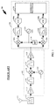
- Receiver 100 can be used at the base station or the remote station.
- the transmitted RF signal is received by antenna 112 , routed through duplexer 114 , and provided to front end 102 .
- amplifier (AMP) 116 amplifies the signal and provides the signal to bandpass filter 118 which filters the signal to remove undesirable images and spurious signals.
- the filtered RF signal is provided to mixer 120 which downconverts the signal to as intermediate frequency (IF) with the sinusoid from local oscillator (LO1) 122.
- IF intermediate frequency
- LO1 local oscillator
- the IF signal from mixer 120 is filtered by bandpass filter 124 and amplified by automatic gain control (AGC) amplifier 126 to produce the required signal amplitude at the input of analog-to-digital-converters (ADCs) 140.
- ADCs analog-to-digital-converters
- the gain controlled signal is provided to demodulator 104.
- two mixers 128a and 128b downconvert the signal into the baseband 1 and Q signals with the sinusoid provided by local oscillator (LO2) 134 and phase shifter 136 , respectively.
- the baseband I and Q signals are provided to lowpass filters 130a and 130b , respectively, which provide match filtering and/or anti-alias filtering of the baseband signals.
- the filtered signals are provided to ADCs 140a and 140b which sample the signals to produce the digitized baseband samples.
- the samples are provided to baseband processor 150 for further processing (e.g. error detection, error correction, and decompression) to produce reconstructed estimates of the transmitted data.
- the first frequency downconversion with mixer 120 allows receiver 100 to downconvert signals at various RF frequencies to a fixed IF frequency where more signal processing can be performed.
- the fixed IF frequency allows bandpass filter 124 to be implemented as a fixed bandpass filter, such as a surface acoustic wave (SAW) filter, to remove undesirable images and spurious signals from the IF signal. Removal of images and spurious signals is important since these signals can fold into the signal band (e.g. the band where the input signal is present) at the second frequency downconversion stage.
- the images and spurious signals can significantly increase the amplitude of the signal into various active components, such as the amplifiers and mixers, which can cause higher level of intermodulation products as the result of non-linearity in the active components. Spurious signals and intermodulation products can cause degradation in the performance of the communication system.
- the quadrature demodulator of the prior art has several major drawbacks.
- quadrature balance is difficult to maintain over many production units because of component tolerance in phase splitter 136 , mixers 128 , lowpass filters 130 , and ADCs 140 . Any mismatch in the two signal paths results in quadrature imbalance and degradation in the performance of receiver 100 .
- Path mismatch results in cross-talk of the I signal onto the Q signal, and vice versa.
- the cross-talk signal behaves as additive noise in the desired signal and results in poor detection of the desired signal.
- ADCs 140 can cause degradation in the performance of receiver 100 for various reasons described below.
- one or more ADCs are required to convert an analog waveform in continuous time into discrete samples at evenly spaced time intervals.
- Some important performance parameters of an ADC include dynamic range, linearity, and DC offset. Each of these parameters can affect the performance of the communication system. Dynamic range can affect the bit-error-rate (BER) performance of the receiver because the noise from the ADC degrades the ability of the ADC to properly detect the input signal. Linearity relates to the difference between an actual transfer curve (e.g., digital output versus analog input) and the ideal transfer curve. Good linearity is more difficult to obtain as the number of bits in the ADC increases. Poor linearity can degrade the error detection/correction process. Finally, DC offset can degrade the performance of the phase locked loop in the receiver and the error correcting decoder, such as the Viterbi decoder.
- flash ADCs or successive approximation ADCs are used to sample the baseband signals.
- L 2 m and m is the number of bits in the ADC.
- the L-1 comparison voltages are generated by a resistive ladder comprising L resistors. Flash ADCs are bulky and consume high power because L-1 comparators and L resistors are required. Flash ADCs can have poor linearity and poor DC offset characteristics if the resistors in the resistive ladder are not matched. However, flash ADCs are popular because of their high operating speed.
- Successive approximation ADCs are also popular for communication systems. These ADCs minimize complexity by performing approximations of the input signal over two or more stages. However, these ADCs can also exhibit poor linearity and poor DC offset characteristics similar to those of the flash ADCs. Thus, flash ADCs and successive approximation ADCs are not ideal candidates for use in many communication applications.
- Sigma delta analog-to-digital converters have better performance than flash and successive approximation ADCs because of the inherent architecture of the ⁇ ADC.
- ⁇ ADC performs analog-to-digital conversion of the input signal by making successive one-bit approximations of the change in the input signal, since the previous sample has been estimated, at a sampling frequency which is many times higher than the bandwidth of the input signal.
- the output samples comprise the input signal and the quantization noise.
- the ⁇ ADC can be designed such that the quantization noise in the signal band is pushed to out-of-band frequency (or noise shaped) where filtering can be performed.
- US-A-5 283 578 discloses an architecture for oversampled ⁇ A/D conversion of high-frequency, narrow-band signals, including multistage ⁇ modulators that incorporate band-reject noise shaping.
- ⁇ ADC can provide high dynamic range, good linearity, and low DC offset because of the inherent structure of the ⁇ ADC.
- high dynamic range can be obtained by selecting a sufficient oversampling ratio (OSR) and the proper noise shaping filter characteristic.
- the oversampling ratio is defined as the sampling frequency divided by the two-sided bandwidth of the input.
- good linearity and low DC offset can be obtained because of the simple one-bit quantizer within the ⁇ ADC.
- ⁇ ADCs have been traditionally limited to applications where the input signal is a low bandwidth signal, such as audio application.
- ⁇ ADCs can be implemented to operate at high speed.
- High speed bandpass and baseband ⁇ ADC designs and implementations are disclosed in detail in copending U.S. Patent Application Serial No. 08/928,847, entitled “SIGMA-DELTA ANALOG-TO-DIGITAL CONVERTER", filed September 12, 1997, assigned to the assignee of the present invention and incorporated by reference herein.
- the bandpass ⁇ ADC provides IF samples which are noise shaped.
- the IF samples are then filtered and quadrature downconverted to provide I and Q baseband outputs.
- the present invention is a novel and improved noise cancellation circuit and quadrature downconverter.
- the noise cancellation comprises at least one bandpass decimator and a summer.
- a bandpass Multi-stAge noise SHaping sigma-delta analog-to-digital converter (MASH ⁇ ADC) is used to sample the analog input signal and each loop in the MASH ⁇ ADC provides an output signal Y. The output from each loop is provided to a corresponding bandpass decimator.
- each bandpass decimator comprises an error cancellation filter, a bandpass filter, and a decimator.
- the bandpass filter is used to filter the signal from the error cancellation filter.
- the filtered signal is then decimated by N by the decimator.
- the signals from all bandpass decimators are summed together and the resultant output comprises the IF samples.
- the IF samples are provided to two multipliers which downconvert the IF samples to I and Q baseband samples with an inphase and a quadrature sinusoid, respectively.
- the baseband samples are lowpass filtered to further remove quantization noise and undesirable signals.
- the transfer function of the error cancellation circuit is decomposed into a set of transfer functions, one for each output signal Y from the ⁇ ADC.
- Each transfer function corresponds to an error cancellation filter.
- the transfer functions for each of the error cancellation filters and the bandpass filter are convolved to provide the transfer function of a bandpass decimator.
- the convolved transfer function for each bandpass decimator can be implemented with less hardware than the direct implementation of the corresponding error cancellation filter and bandpass filter.
- each bandpass decimator operates on one-bit signal Y from a corresponding loop of the MASH ADC.
- the bandpass filter In addition, the decimation by N can be incorporated within the bandpass decimator such that the bandpass decimators only operate at 1/N of the frequency of the ADC sampling clock, thereby reducing power consumption.
- the present invention is a new and improved noise cancellation circuit and quadrature downconverter which are used in conjunction with an analog-to-digital converter (ADC).
- ADC analog-to-digital converter
- the present invention is well suited for used in combination with a sigma-delta analog-to-digital converter ( ⁇ ADC) which is disclosed in the aforementioned U.S. Patent Application Serial No. PA447.
- Exemplary applications which can utilize the noise cancellation circuit and quadrature downconverter include CDMA communication systems and HDTV systems.
- a bandpass sampling ADC In a bandpass sampling ADC, the input signal to the ADC is centered at an intermediate frequency (IF) instead of baseband. Sampling at IF allows for elimination of a frequency downconversion stage in the receiver, thus simplifying the hardware design and improving reliability.
- ⁇ ADC provides many advantages over conventional (e.g. flash and successive approximation) ADCs as described above.
- the noise shaper within the ⁇ ADC can be designed such that the quantization noise around the signal band is pushed out-of-band (or noise shaped) where filtering can be performed.
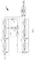
- Receiver 200 can be used to demodulate BPSK, QPSK, OQPSK, QAM, and other digital and analog modulation formats.
- the transmitted RF signal is received by antenna 212 , routed through duplexer 214 , and provided to front end 202 .
- amplifier (AMP) 216 amplifies the signal and provides the amplified signal to bandpass filter 218 which filters the signal to remove undesirable images and spurious signals.
- the filtered signal is provided to mixer 220 which downconverts the signal to an IF frequency with the sinusoid from local oscillator (LO1) 222 .
- LO1 local oscillator
- the IF signal from mixer 220 is provided to bandpass filter 224 which further filters the signal.
- bandpass filter 224 is a surface acoustic wave (SAW) filter, the implementation of which is known in the art.
- the filtered signal is provided to buffer (BUF) 226 which provides gain and/or buffering of the signal.
- the buffered signal is provided to demodulator 204 .
- ADC 240 samples the buffered signal at a high sampling frequency determined by the CLK signal and provides the samples to digital signal processor (DSP) 250 .
- DSP digital signal processor
- a bandpass ADC For applications wherein quadrature demodulation is required, such as QPSK, OQPSK and QAM, a bandpass ADC is utilized.
- the bandpass ADC can be designed and implemented as a bandpass ⁇ ADC in the manner described in copending U.S. Patent Application Serial No. PA447.
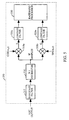
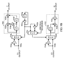
- MASH ADC 240a comprises two loops 310a and 310b , feed forward element 320 , and error cancellation circuit 350 .
- MASH ADC 240a receives an analog ADC input and produces a digital ADC output having at least two bits per sample, at least one bit per sample for each loop 310 .
- the ADC input is provided to loop 310a which produces a 1-bit Y1 signal in response thereto.
- a fraction of the ADC input and quantization noise (X2) from loop 310a is provided to loop 310b where additional noise shaping is performed.
- the Y1 and Y2 signals from loops 310a and 310b, respectively, are provided to error cancellation circuit 350 .
- Error cancellation circuit 350 delays, filters, and combines the Y1 and Y2 signals to produce the ADC output.
- summer 312a receives the ADC input and the Y1 signal from quantizer 316a , subtracts Y1 from the ADC input, and provides the error signal to resonator 314a .
- Resonator 314a filters the error signal and provides the filtered signal to summer 312b .
- each resonator 314 in MASH ADC 240a is implemented with the bandpass transfer function k n • z -2 / 1+ z -2 , where k n is the gain of the n-th resonator 314 within loop 310.
- Summer 312b also receives Y1 from quantizer 316a, subtracts Y1 from the error signal from resonator 314a, and provides the error signal to resonator 314b which further filters the error signal.
- the filtered signal from resonator 314b is provided to quantizer 316a which produces the 1-bit Y1 signal in response thereto.
- Loop 310b is connected in similar manner as loop 310a .
- the filtered output from resonator 314b is also provided to gain element 322a which scales the signal by the scaling factor a 1 .
- the Y1 signal from quantizer 316a is provided to gain element 322b which scales Y1 by the scaling factor a 2 .
- the outputs from gain elements 322a and 322b are provided to summer 324 which subtracts the output from gain element 322b from the output from gain element 322a .
- the error signal from summer 324 is provided to gain element 322c which scales the error signal by the scaling factor a 3 .
- the output from gain element 322c comprises X2 which is provided to loop 310b .
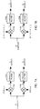
- FIG. 4 A block diagram of an exemplary error cancellation circuit 350 is shown in FIG. 4.
- the Y1 signal from loop 310a is provided to delay element 412 which delays Y1 by a time interval equal to the processing delay of loop 310b.
- the delayed Y1 from delay element 412 is time aligned with Y2.
- the Y2 signal from loop 310b is provided to gain element 416 which scales Y2 by the scaling factor G.
- the delayed Y1 is provided to gain element 414 which scales the delayed Y1 by the scaling factor (h-1).
- the scaling factors G and (h-1) partially determine the noise shaping characteristics of ⁇ ADC 240a.
- the outputs from gain elements 414 and 416 are provided to summer 418 which sums the two scaled outputs.
- the combined signal from summer 418 is provided to filter 420 which filters the combined signal with the transfer function N(z).
- Other transfer functions for filter 420 and delay element 412 can also be utilized and are within the scope of the present invention.
- every second coefficient of N(z) is zero and this characteristic is used to simplify the design of the error cancellation circuit and bandpass filter of the present invention.
- the output from filter 420 and the delayed Y1 are provided to summer 422 which sums the two signals to produce the ADC output.
- the exemplary transfer function Y(z) for error cancellation circuit 350 can be expressed as :
- the term in the first bracket comprises the signal component and the term in the second bracket comprises the total quantization noise after error cancellation.
- the transfer function Y(z) of error cancellation circuit 350 can be viewed as running the Y1 signal through a first finite impulse response (FIR) filter having the coefficients EC Y1 (z), running the Y2 signal through a second FIR filter having the coefficients EC Y2 (z), and summing the two FIR filter outputs.
- FIR finite impulse response
- the coefficients for the FIR filters can be expressed as: From equation (2), it can be noted that although the inputs into error cancellation circuit 350 comprise two signals, Y1 and Y2, each having one bit of resolution, the output from error cancellation circuit 350 comprises five bits of resolution and has a range of 0 to 21. From equation (1), it can be noted that the amplitude of the signal is not amplified. However, the quantization noise is processed and shaped, and additional range is required for the shaped out-of-band quantization noise.
- bandpass filter 512 An exemplary block diagram of digital signal processor 250 used for quadrature demodulation is illustrated in FIG. 5.
- the ADC output from ADC 240 is provided to bandpass filter 512 which filters the signal to remove quantization noise and other spurious signals.
- the transfer function in equation (3) provides zeros at f ADC /12 and 5f ADC /12 and has a maximum gain at f ADC /4.
- the characteristic of bandpass filter 512 is selected in conjunction with decimator 514 , as described below.
- Other bandpass filter transfer functions can also be utilized and are within the scope of the present invention.
- bandpass filter 512 after error cancellation circuit 350 provides many advantages.
- the received signal is centered at f ADC /4 after conversion by ADC 240a .
- the amplitude response of bandpass filter 512 is designed to provide a passband around f ADC /4 and the transfer function of bandpass filter 512 comprises zero for every other coefficient.
- This filter coefficient characteristics can be combined with a similar characteristic of error cancellation circuit 350 , as shown in equation (2), to simplify the overall design of error cancellation circuit 350 and bandpass filter 512 .
- the output from error cancellation circuit 350 can comprise five bits of resolution. Designing bandpass filter 512 to compute the required 5-bit precision arithmetic can greatly increase the complexity of bandpass filter 512 .
- error cancellation circuit 350 and bandpass filter 512 are combined such that the resultant circuit operates on the 1-bit Y1 and Y2 signals directly.
- bandpass filter 512 removes a large portion of the quantization noise from ADC 240a such that the required dynamic range after bandpass filter 512 is reduced accordingly.
- the filtered signal from bandpass filter 512 is provided to decimator 514 which decimates the signal by a factor of N to 1, where N is an odd number in the exemplary embodiment. For every N input samples, decimator 514 retains 1 sample and discards the remaining N-1 samples.
- the output from decimator 514 comprises the IF samples which are provided to multipliers 518a and 518b . Multipliers 518a and 518b downconvert the IF samples to I and Q baseband samples with the inphase cos(w c t) and quadrature sin(w c t) sinusoids, respectively.
- the I and Q baseband samples are provided to lowpass filters 520a and 520b , respectively, which filter the samples to provide the I and Q outputs.
- the I and Q outputs are provided to baseband processor 530 which performs additional signal processing, such as filtering, decimation, error detection/correction, and decompression.
- bandpass filter 512 and/or lowpass filters 520 can also provide scaling of the signal to enable digital signal processor 530 to provide baseband data at various amplitude.
- Other implementations of digital signal processor 250 can be designed to performed quadrature demodulation and are within the scope of the present invention.
- Error cancellation circuit 350 and bandpass filter 512 can be implemented with direct implementation, as shown in FIGS. 5 and 6. However, direct implementation would yield a complicated design since two circuits are required for error cancellation circuit 350 and bandpass filter 512 and bandpass filter 512 would be designed to operate on a signal having five bits of resolution. In the present invention, error cancellation circuit 350 and bandpass filter 512 are combined.
- FIG. 6 An exemplary block diagram of the digital signal processing of the Y1 and Y2 signals using noise cancellation circuit 600 is illustrated in FIG. 6.
- the Y1 and Y2 signals are provided to bandpass decimators 602 and 604 , respectively.
- one bandpass decimator is provided for each loop of MASH ADC 240a .
- the Y1 signal is provided to error cancellation filter 608 which filters Y1 with the transfer function EC Y1 (z) as shown in equation (2).
- the filtered Y1 is provided to bandpass filter 612a.
- bandpass filters 612 each has the same transfer function as bandpass filter 512 , as shown in equation (3).
- bandpass decimator 604 is identical to bandpass decimator 602 except that error cancellation filter 610 implements the transfer function EC Y2 (z) as shown in equation (2).
- the transfer functions of error cancellation filter 608 and bandpass filter 612a are convolved to generate the transfer function of bandpass decimator 602.
- the transfer functions of error cancellation filter 610 and bandpass filter 612b are convolved to generate the transfer function of bandpass decimator 604 .
- the improvement achieved by implementing bandpass decimators 602 and 604 with the convolved transfer functions can be illustrated for an exemplary third order bandpass filter 612 .
- H BPF3 ( z ) [1 0 -3 0 6 0 -7 0 6 0 -3 0 1] .
- H Y1 (z) and H Y2 (z) can be expressed as FIR filters having the coefficients shown in equation (5).
- H Y1 [0 0 0 0 2 0 -4 0 7 0 -5 0 4 0 -1 0 2 0 -1 0 1]
- H Y 2 [10 -1 0 1 0 2 0 -2 0 2 0 1 0 -1 0 1]•4
- the implementation of the convolved filter H Y1 (z) requires 11 adders (e.g., one adder for each coefficient of 1, -1, 2, 4 or -4 and two adders for each coefficient of -5 or 7).
- the implementation of the convolved filter H Y2 (z) requires 9 adders (e.g., one adder for each coefficient of 1, -1, 2 or -2).
- the number of adders required for the convolved filters (error cancellation filter and bandpass filter) is less than that required for the bandpass filter alone.
- the convolved filters H Y1 (z) and H Y2 (z) operate on the Y1 and Y2 signals, respectively, each having only one bit of resolution.
- decimators 614 can be incorporated within convolved filters H Y1 (z) and H Y2 (z) such that an output sample is computed once every N input samples. Operating the convolved filters at 1/N of the frequency of the ADC sampling clock minimizes power consumption.
- ADC 240 is a bandpass ⁇ ADC 240a which shapes the quantization noise in the manner disclosed in copending U.S. Patent Application Serial No. PA447.
- the quantization noise around 0.25•f ADC is pushed toward DC and 0.50•f ADC where filtering of the quantization noise can be performed.
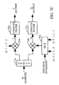
- the quadrature downconverter as shown in FIG. 5 is redrawn in FIG. 7A.
- the IF samples from decimator 514 are downconverted to baseband samples by multipliers 518a and 518b with the inphase cos(w c t) and quadrature sin(w c t) sinusoids, respectively.
- the frequency downconversion stage can be made trivial.
- the quadrature downconversion by multipliers 518a and 518b can be performed by multiplying the IF samples with the inphase sequence [1, 0, -1, 0, 1, 0, ...] and quadrature sequence [0, 1, 0, -1, 0, 1, ...], respectively, as shown in FIG. 7B.
- every other value of the inphase sequence [1, 0, -1, 0, 1, 0, ...] is zero.
- every other value of the quadrature sequence [0, 1, 0, -1, 0, 1, ...] is zero.
- the inphase and quadrature sequences are valid (e.g., not zero) on alternative values. These characteristics can be used to simplify the design of the quadrature downconverter.
- a block diagram of an exemplary quadrature downconverter which takes advantage of the above characteristics is shown in FIC. 7C.
- the quadrature downconverter is designated such that every other IF sample is provided by demultiplexer (DEMUX) 716 to multiplier 718a and every other alternative IF sample is provided to multiplier 718b .
- multipliers 718a and 718b can be operated at half the speed as multipliers 518a and 518b , thereby reducing power consumption.
- Lowpass filters 720 and 722 are equivalent to lowpass filters 520a and 520b , respectively.
- lowpass filter 720 is designed with an additional delay of one half sample cycle with respect to the delay of lowpass filter 722 .
- the amplitude response of lowpass filters 720 and 722 are designed to be approximately similar to minimize IQ imbalance and IQ crosstalk. The additional delay can be provided by using different filter transfer functions for filters 720 and 722 .
- the additional delay can be provided by using the same filter transfer function for filters 720 and 722 , which are clocked at least twice the sample rate, and delaying the output of filter 720 by one half sample.
- filters 720 and 722 which are clocked at least twice the sample rate, and delaying the output of filter 720 by one half sample.
- filters 720 and 722 can be contemplated and are within the scope of the present invention.
- Spectral inversion of the spectrum of the sampled signal can occur when the signal is subsampled. The occurrence of spectral inversion is dependent on the sampling frequency of the ADC relative to the center frequency of the signal being sampled.
- the spectral inversion can be corrected by selecting a quadrature sinusoid which is 180° out of phase, or an inverted quadrature sinusoid.
- the quadrature sinusoid or the inverted quadrature sinusoid can selected through multiplexer (MUX) 724 by the spectral inversion signal, as shown in FIG. 7C.
- MUX multiplexer
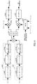
- FIG. 8 An exemplary noise cancellation circuit and quadrature downconverter design for a CDMA application is shown in FIG. 8.
- the signal processing illustrated in FIG. 8 is a combination of the noise cancellation circuits shown in FIGS. 6 and the quadrature downconverter shown in FIG. 7C.
- the ADC is implemented as a MASH 4-4 ⁇ ADC as described in the aforementioned U.S. Patent Application Serial No. PA447.
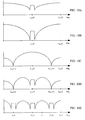
- the ⁇ ADC can operate in one of several modes. In the high dynamic range mode, the ⁇ ADC provides the Y1 and Y2 signals, as shown in FIG. 3. In the medium or low dynamic range mode, the ⁇ ADC can provide either the Y1 or Y2 signal. An exemplary spectrum of the Y1 signal is shown in FIG. 10A.
- bandpass decimator 802 comprises error cancellation filter 808 , bandpass filter 812a , and decimator 814a and bandpass decimator 804 comprises error cancellation filter 810 , bandpass filter 812b , and decimator 814b .
- error cancellation filters 808 and 810 are designed with the transfer functions EC Y1 (z) and EC Y2 (z) as shown in equation (1), respectively.
- An exemplary spectrum of the Y1 signal after error cancellation filter 808 is shown in FIG. 10B.
- bandpass filters 812a and 812b are connected to error cancellation filters 808 and 810 , respectively, and are each designed as a fifth order bandpass filter having the transfer function shown in FIG. 8.
- the fifth order bandpass filters 812 are different from the exemplary third order bandpass filter shown in equations (4) and (5) above.
- the higher order filters are utilized to more fully capture the performance of the ⁇ ADC.
- the error cancellation circuit produces a deep notch around the desired signal band (thereby lowering the noise floor of the desired signal band) and pushes the quantization noise out-of-band.
- the fifth order bandpass filter is used to filter the out-of-band quantization noise such that the noise that is folded into the desired signal band by the subsequent decimation stage is comparable in magnitude to noise floor of the ⁇ ADC.
- An exemplary frequency response of bandpass filter 812 is shown in FIG. 10C and an exemplary spectrum of the Y1 signal after bandpass filter 812a is shown in FIG. 10D.
- Different bandpass filter transfer functions and different filter order can be utilized and are within the scope of the present invention.
- decimators 814 are each implemented as a 3 to 1 decimator. Decimation by an odd integer (e.g., 3, 5, 7, 9, etc.) maintains the CDMA signal at one quarter of the sample rate after the decimation such that the subsequent quadrature downconversion step can be easily performed. Initially, the CDMA signal is centered around f ADC /4 after the ADC conversion, as shown in FIGS. 10A and 10B. After decimation by three, the COMA signal is folded such that the signal centered at f ADC /4 is translated to f ADC /12 or f s /4, where f s is the sample rate of the decimated samples.
- odd integer e.g., 3, 5, 7, 9, etc.
- the noise at f ADC /12 is filtered by placing a notch at that frequency location in bandpass filter 812 , as shown in FIG. 10C. Furthermore, it can be noted that the signal at 5f ADC /12 also folds down to f ADC /12 after the decimation by three. Thus, bandpass filter 812 is designed with a second notch at 5f ADC /12 to filter out undesirable signals at this frequency location which will fold down to f ADC /12.
- the exemplary spectrum of the Y1 signal after decimation by three is shown in FIG. 10E.
- the transfer function of bandpass filters 812 is selected based on the selection of decimators 814 .
- the transfer function of bandpass filter 812 is designed with a zero at f s /4 and at each frequency location which folds down to f s /4 after decimation by N.
- bandpass filter 812 is designed such that a zero is placed at mf ADC /4N, where m is an positive odd integer less than 2N and m ⁇ N.
- zeros are placed at f ADC /12 and 5f ADC /12.
- zeros are placed at f ADC /20, 3f ADC /20, 7f ADC /20, and 9f ADC /20.
- the coefficients for the bandpass filter which comprise the zeros at the desired frequency locations can be synthesized as follows. First, start with the same number of ones as the decimation N, e.g., [111] for decimation by three. Second, invert every other filter coefficient, e.g., [1 -11]. And third, insert a zero between each pair of coefficients, e.g., [10-101].
- the filter coefficients after the third step comprise the filter transfer function which provides the zeros at the desired frequency locations. For a decimation by five, the filter coefficients are [10 -10 10 -10 1]. Similarly, for a decimation by seven, the filter coefficients are [10-1010-1010-101]. It should be noted that this synthesis method is only applicable for odd N. However, decimation by odd N is preferred since the image of the decimated signal is maintained at f s /4 to simplify the design of the quadrature downconverter.
- the outputs from decimators 814a and 814b are provided to summer 815 and combined.
- the IF samples from summer 815 are provided to demultiplexer (DEMUX) 816 which directs alternative samples to multipliers 816a and 816b .
- DEMUX 816 , multipliers 818 , and multiplexer (MUX) 824 perform the functions as described for DEMUX 716 , multipliers 718 , and MUX 724 as shown in FIG. 7C.
- the outputs from multipliers 818a and 818b are provided to lowpass filters 820 and 822 , respectively.
- lowpass filters 820 and 822 have the transfer functions as shown in FIG. 8.
- the transfer function of lowpass filter 820 has substantially similar amplitude response to the transfer function of lowpass filter 822 . However, the transfer function of lowpass filter 820 provides an additional delay of one sample with respect to the delay of lowpass filter 822 such that the I output is time aligned with the Q output.
- the noise cancellation circuit and quadrature downconverter shown in FIG. 8 can be implemented in many manner.
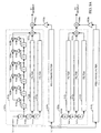
- An exemplary implementation of the noise cancellation circuit and quadrature downconverter using a polyphase structure is shown in FIGS.9A-B, respectively.
- the polyphase structure is a functional and bit-exact equivalent to the direct implementation and takes advantage of the characteristic that every other coefficient in the transfer functions of error cancellation filters 808 and 810 and filter 812 is zero.
- the polyphase structure performs simple signal processing on multiple phases of the input signal and combines the intermediate outputs to yield the desired output.
- Decimator 814 can be integrated within the polyphase structure using a clocking scheme wherein the Y1 and Y2 signals are decimated by six before any processing is performed. The pre-decimation allows the registers of the polyphase structure to be operated at a lower clock speed which reduces power consumption.
- the Y1 signal is provided to polyphase filters 902a and 904a and the Y2 signal is provided to polyphase filters 902b and 904b .
- all registers labeled "A" in FIG. 9A are clocked on the rising edge of a clock (f ADC /2) which is half the frequency of the ADC sampling clock
- all registers labeled "B” are clocked on the falling edge of the f ADC /2 clock
- all registers labeled "C” are clocked on the rising edge of a clock (f ADC /6) which is one-sixth the frequency of the ADC sampling clock.
- Y1 is provided to register 914a .
- the output from register 914a is provided to register 914b and the output from register 914b is provided to register 914c .
- Registers 914 provide three phases of the Y1 signal.
- the three phases of Y1 from register 914a , 914b , and 914c are provided to filters 912a , 912b , and 912c , respectively.
- the output from register 914a is provided to register 916a
- the output from register 916a is provided to register 916b and gain element 918a
- the output from register 916b is provided to register 916c and gain element 918b
- the output from register 916c is provided to register 916d and gain element 918c
- the output from register 916d is provided to register 916e and gain element 918d
- the output from register 916e is provided to register 916f and gain element 918e
- the output from register 916f is provided to gain element 918f .
- the gains of gain elements 918a, 918b, 918c, 918d, 918e, and 918f within filter 912a are [0, -8, 45, -21, 7, 0], respectively.
- the gains of filter 912b are [0, 21, -42,15,-3,0]
- the gains of filter 912c are [2,-35,33,-10,1,0].
- the gains of the three corresponding filters in polyphase filter 902b are [1, -5, -12, -5, 1, 0], [-3, 0, 9, 6, 0, 0], and [6,9,0,-3, 0, 0].
- the exemplary gains of filter 912d are [0, 2, -35, 33, -10,1], the exemplary gains of filter 912e are [0, -8, 45, -21, 7, 0], and the exemplary gains of filter 912f are [0, 21, -42, 15, -3, 0].
- the exemplary gains of the three filters within polyphase filter 904b are [0, 6, 9, 0, -3, 0], [1,-5,-12,-5,1,0], and [-3,0,9,6,0,0].
- the polyphase filters can be implemented such that the coefficients can be rearranged and/or combined to simplify the hardware design.
- the filter gains of [-3, 0, 9, 6, 0, 0] can be implemented as 3•[-1, 0, 3, 2, 0, 0].
- the data samples corresponding to the -1 and 2 coefficients can be scaled and combined, the resultant sum can be combined with the scaled data sample corresponding to the 3 coefficient, and the overall result scaled by three.
- Adder 920b receives the outputs from gain elements 918a and 918b , sums the two signals, and provides the output to adder 920c .
- Adder 920c also receives the output from gain element 918c , sums the two signals, and provides the output to adder 920d.
- Adder 920d also receives the output from gain element 918d , sums the two signals, and provides the output of filter 912a.
- the outputs of filters 912a, 912b, and 912c are provided to adder 922a which sums the three signals to provide the output of polyphase filter 902a.
- Polyphase filters 902b is identical to polyphase filter 902a .
- Polyphase filters 904 are identical to polyphase filters 902 with the exception that the "A" registers 914 in polyphase filter 902 are replaced with the "B" registers 906 in polyphase filter 904.
- Polyphase filters 902 and 904 perform most of the functions of error cancellation filters 808 and 810 and bandpass filters 812 in FIG. 8, respectively.
- the output from polyphase filters 902b and 904b are provided to gain elements 932a and 932b , respectively. Each gain element 932 scales the respective output with an exemplary gain of four to account for the gain of error cancellation filter 810 .
- the output from polyphase filter 902a and the output from gain element 932a are provided to adder 930a which sums the two signals.
- the output from polyphase filter 904a and the output from gain element 932b are provided to adder 930b which sums the two signals.
- the outputs from adders 930a and 930b comprise the two outputs from the noise cancellation circuit and correspond to the outputs from DEMUX 816 in FIG. 8.
- the output from adder 930a is provided to multiplexer (MUX) 936a and gain element 934a which scales the signal with a gain of -1.
- the output from gain element 934a is provided to MUX 936a .
- MUX 936a alternatively selects the output from gain element 934a and the output from adder 930a and effectively performs the function of multiplier 818a in FIG. 8.
- Register 916g and inverter 952a provides a sequence of alternating ones and zeros [1 01 0 ...] which is used to control MUX 936a .
- the output from MUX 936a is provided to lowpass filter 908 which implements the transfer function of lowpass filter 820 in FIG. 8.
- the output from MUX 936a is provided to register 916e and adder 920e .
- the output from register 916e is provided to register 916f and gain element 918e which scales the signal with a gain of six.
- the output from gain element 918e is provided to adder 920e which sums the two inputs and provides the output to adder 920f.
- the output from register 916f is provided to adder 920f which sums the two inputs and provides the I output.
- the output from adder 930b is provided to multiplexer (MUX) 936b and gain element 934b which scales the signal with a gain of -1.
- the output from gain element 934b is provided to MUX 936b.
- MUX 936b alternatively selects the output from gain element 934b and the output from adder 930b and effectively performs the function of multiplier 818b in FIG. 8.
- the sequence of alternating ones and zeros [101 0 ...] from inverter 952a is provided to MUX 954 and inverter 952b .
- the output of inverter 952b is provided to MUX 954.
- MUX 954 implements the function of MUX 824 in FIG.
- the output from MUX 936b is provided to lowpass filter 910 which implements the transfer function of lowpass filter 822 in FIG.8.
- lowpass filter 970 the output from MUX 936b is provided to register 916h and adder 920h.
- the output from register 916h is also provided to adder 920h which sums the two input and provides the output to gain element 938 .
- Gain element 938 scales the signal with a gain of four and provides the Q output.
- the present invention has been described for a bandpass sampling receiver utilizing a ⁇ ADC.
- the transfer function of the error cancellation filter is selected accordingly and a bandpass filter is used to filter the quantization noise before the quadrature downconversion.
- the present invention is also applicable for a baseband receiver utilizing a ⁇ ADC.
- the transfer function of the error cancellation filter is modified for the baseband ⁇ ADC and a lowpass filter is used to filter the quantization noise.
- the transfer functions of the baseband error cancellation filter and the lowpass filter can be convolved to generate the noise cancellation circuit in similar manner to that described above for the bandpass receiver design.
- the adaptation of the inventive concept described above for use in a baseband receiver is within the scope of the present invention.
Landscapes
- Engineering & Computer Science (AREA)
- Theoretical Computer Science (AREA)
- Compression, Expansion, Code Conversion, And Decoders (AREA)
- Noise Elimination (AREA)
- Analogue/Digital Conversion (AREA)
- Digital Transmission Methods That Use Modulated Carrier Waves (AREA)
Applications Claiming Priority (3)
| Application Number | Priority Date | Filing Date | Title |
|---|---|---|---|
| US5355 | 1998-01-09 | ||
| US09/005,355 US6243430B1 (en) | 1998-01-09 | 1998-01-09 | Noise cancellation circuit in a quadrature downconverter |
| PCT/US1999/000580 WO1999035746A1 (en) | 1998-01-09 | 1999-01-11 | Noise cancellation circuit and quadrature downconverter |
Publications (2)
| Publication Number | Publication Date |
|---|---|
| EP1046232A1 EP1046232A1 (en) | 2000-10-25 |
| EP1046232B1 true EP1046232B1 (en) | 2005-03-16 |
Family
ID=21715446
Family Applications (1)
| Application Number | Title | Priority Date | Filing Date |
|---|---|---|---|
| EP99903040A Expired - Lifetime EP1046232B1 (en) | 1998-01-09 | 1999-01-11 | Noise cancellation circuit and quadrature downconverter |
Country Status (14)
| Country | Link |
|---|---|
| US (1) | US6243430B1 (enExample) |
| EP (1) | EP1046232B1 (enExample) |
| JP (1) | JP4162851B2 (enExample) |
| KR (1) | KR100545492B1 (enExample) |
| CN (1) | CN1168215C (enExample) |
| AU (1) | AU758706B2 (enExample) |
| BR (1) | BR9906807A (enExample) |
| CA (1) | CA2315758C (enExample) |
| DE (1) | DE69924233T2 (enExample) |
| ES (1) | ES2237906T3 (enExample) |
| IL (1) | IL136712A0 (enExample) |
| NO (1) | NO326664B1 (enExample) |
| RU (1) | RU2233023C2 (enExample) |
| WO (1) | WO1999035746A1 (enExample) |
Families Citing this family (83)
| Publication number | Priority date | Publication date | Assignee | Title |
|---|---|---|---|---|
| FI120124B (fi) * | 1998-05-29 | 2009-06-30 | Nokia Corp | Menetelmä ja piiri signaalin näytteistämiseksi suurella näytteistystaajuudella |
| FR2780590B1 (fr) * | 1998-06-29 | 2000-10-06 | Sgs Thomson Microelectronics | Demodulateur qpsk a entree en frequence intermediaire |
| EP1067674B1 (en) * | 1999-06-30 | 2003-06-04 | Motorola, Inc. | Apparatus and method for receiving and processing a radio frequency signal |
| US6904104B1 (en) * | 1999-09-10 | 2005-06-07 | Telefonaktiebolaget L M Ericsson (Publ) | Technique for demodulating a linear modulated data signal in a communications system |
| SE9903532D0 (sv) * | 1999-09-28 | 1999-09-28 | Jiren Yuan | Versatile charge sampling circuits |
| US6728325B1 (en) * | 2000-02-02 | 2004-04-27 | Legerity, Inc. | Method and apparatus for mixing down and spectrum folding frequency diverse modulated carrier |
| EP1208652B1 (en) * | 2000-02-04 | 2004-03-31 | Philips Electronics N.V. | Radio fm receiver |
| FR2808391B1 (fr) * | 2000-04-28 | 2002-06-07 | France Telecom | Systeme de reception pour antenne multicapteur |
| GB2403612B (en) * | 2000-05-12 | 2005-02-16 | Global Silicon Ltd | Radio receiver |
| US7693236B2 (en) * | 2000-05-15 | 2010-04-06 | Texas Instruments Incorporated | If-to-baseband conversion for flexible frequency planning capability |
| US6724177B2 (en) * | 2000-12-14 | 2004-04-20 | Tropian, Inc. | Method and apparatus for accurate measurement of communications signals |
| US7110732B2 (en) * | 2001-04-09 | 2006-09-19 | Texas Instruments Incorporated | Subsampling RF receiver architecture |
| US7346134B2 (en) * | 2001-05-15 | 2008-03-18 | Finesse Wireless, Inc. | Radio receiver |
| WO2002095972A1 (en) * | 2001-05-25 | 2002-11-28 | The National University Of Singapore | Sigma-delta modulation code division multiple-access receiver |
| US6429797B1 (en) * | 2001-07-05 | 2002-08-06 | International Business Machines Corporation | Decimation filter for a bandpass delta-sigma ADC |
| US20030058148A1 (en) * | 2001-09-21 | 2003-03-27 | Sheen Timothy W. | Multiple a-to-d converter scheme employing digital crossover filter |
| US20030096588A1 (en) * | 2001-11-20 | 2003-05-22 | Vanderhelm Ronald J. | Receiver intermod enhancer |
| US6999132B1 (en) * | 2002-02-19 | 2006-02-14 | Lsi Logic Corporation | RF/IF digital demodulation of video and audio |
| KR100686421B1 (ko) | 2002-03-04 | 2007-02-23 | 에스티마이크로일렉트로닉스 엔.브이. | 공진전원변환 및 방법을 위한 코더장치 |
| US7924937B2 (en) | 2002-03-04 | 2011-04-12 | Stmicroelectronics N.V. | Resonant power converter for radio frequency transmission and method |
| KR100454483B1 (ko) * | 2002-03-04 | 2004-10-28 | 삼성전자주식회사 | 아이/큐 복조장치 및 그의 아이/큐 신호생성방법 |
| US7173980B2 (en) * | 2002-09-20 | 2007-02-06 | Ditrans Ip, Inc. | Complex-IF digital receiver |
| US7565170B2 (en) * | 2002-12-24 | 2009-07-21 | Telecom Italia S.P.A. | Radio base station receiver having digital filtering and reduced sampling frequency |
| US7199738B2 (en) * | 2003-03-28 | 2007-04-03 | Siemens Medical Solutions Usa, Inc. | Sigma delta beamformer and method with reduced artifact |
| US7206563B1 (en) * | 2003-04-17 | 2007-04-17 | Apogee Technology, Inc. | Reduction of radio frequency interference (RFI) produced by switching amplifiers |
| CN1549454A (zh) * | 2003-05-16 | 2004-11-24 | 皇家飞利浦电子股份有限公司 | 具有一个有限动态范围的adc的无线通信接收机 |
| CN1625063A (zh) * | 2003-12-05 | 2005-06-08 | 皇家飞利浦电子股份有限公司 | 带通采样接收机及其采样方法 |
| US7180432B2 (en) * | 2004-02-27 | 2007-02-20 | Freescale Semiconductor, Inc. | Method and apparatus for complex cascade sigma-delta modulation and single-sideband analog-to-digital conversion |
| DE602004008214D1 (de) * | 2004-03-18 | 2007-09-27 | St Microelectronics Srl | Verfahren und Vorrichtungen zur Kodierung/Dekodierung von Signalen, sowie Computerprogrammprodukt dafür |
| JP3970266B2 (ja) * | 2004-06-23 | 2007-09-05 | 株式会社半導体理工学研究センター | 複素バンドパスδσad変調器、ad変換回路及びディジタル無線受信機 |
| CN1298109C (zh) * | 2004-06-25 | 2007-01-31 | 天津大学 | 新型锁相检测电路 |
| CN101069352A (zh) * | 2004-11-16 | 2007-11-07 | 皇家飞利浦电子股份有限公司 | 具有抗干扰保护的非浸入性滤波器的连续时间∑△模拟数字转换器 |
| JP2008527885A (ja) * | 2005-01-13 | 2008-07-24 | エヌエックスピー ビー ヴィ | 低中間周波数レシーバおよびそのサンプリング方法 |
| KR100631210B1 (ko) * | 2005-02-18 | 2006-10-04 | 삼성전자주식회사 | IF direct sampling 방식을 적용한 수신기의 복조회로 |
| JP3992287B2 (ja) * | 2005-06-15 | 2007-10-17 | 株式会社半導体理工学研究センター | 複素バンドパスフィルタ、複素バンドパスδσad変調器、ad変換回路及びデジタル無線受信機 |
| US8050649B2 (en) * | 2005-08-30 | 2011-11-01 | Qualcomm Incorporated | Downconversion mixer with IM2 cancellation |
| DE102006029486A1 (de) * | 2006-06-27 | 2008-01-03 | Fraunhofer-Gesellschaft zur Förderung der angewandten Forschung e.V. | Signalaufbereiter und Verfahren zum Verarbeiten eines Empfangssignals |
| DE102006029482A1 (de) * | 2006-06-27 | 2008-01-03 | Fraunhofer-Gesellschaft zur Förderung der angewandten Forschung e.V. | Empfänger und Verfahren zum Empfangen eines ersten Nutzfrequenzbandes und eines zweiten Nutzfrequenzbandes |
| US8295371B2 (en) * | 2006-07-14 | 2012-10-23 | Qualcomm Incorporated | Multi-carrier receiver for wireless communication |
| GB2440187A (en) * | 2006-07-17 | 2008-01-23 | Ubidyne Inc | DUC and DDC forming digital transceiver |
| GB2440192B (en) * | 2006-07-17 | 2011-05-04 | Ubidyne Inc | Antenna array system |
| JP4182448B2 (ja) * | 2006-07-27 | 2008-11-19 | ソニー株式会社 | 受信装置、受信方法、プログラム、並びに、記録媒体 |
| US7656970B1 (en) * | 2006-09-01 | 2010-02-02 | Redpine Signals, Inc. | Apparatus for a wireless communications system using signal energy to control sample resolution and rate |
| JP4304632B2 (ja) * | 2006-10-12 | 2009-07-29 | ソニー株式会社 | 受信装置、受信方法、プログラム、並びに、記録媒体 |
| JP4514801B2 (ja) * | 2008-01-22 | 2010-07-28 | シャープ株式会社 | 放送受信装置 |
| US8879983B2 (en) * | 2008-02-06 | 2014-11-04 | Hmicro, Inc. | Wireless communications systems using multiple radios |
| CN101420405B (zh) * | 2008-12-09 | 2013-08-21 | 中国电子科技集团公司第五十四研究所 | 抗多径符号定时同步装置 |
| US7916050B1 (en) * | 2009-10-15 | 2011-03-29 | Texas Instruments Incorporated | Time-interleaved-dual channel ADC with mismatch compensation |
| US8532238B2 (en) * | 2010-02-08 | 2013-09-10 | Electronics And Telecommunications Research Institute | Subsampling based receiver using frequency selective noise canceller |
| US8489662B2 (en) * | 2010-03-05 | 2013-07-16 | The Aerospace Corporation | Systems and methods for sliding convolution interpolating filters |
| US8855254B2 (en) * | 2010-03-05 | 2014-10-07 | The Aerospace Corporation | Systems and methods for pre-averaged staggered convolution decimating filters |
| EP2369301B1 (de) * | 2010-03-23 | 2014-04-30 | Micronas GmbH | Sensorbaustein und Verfahren zur Funktionsüberwachung eines solchen |
| US20120128040A1 (en) | 2010-11-23 | 2012-05-24 | Peter Kenington | Module for an Active Antenna System |
| KR101136969B1 (ko) * | 2010-12-30 | 2012-04-19 | 전자부품연구원 | 대역통과 변조 장치 |
| CN102904594A (zh) * | 2011-07-29 | 2013-01-30 | 普天信息技术研究院有限公司 | 一种无线数传终端及其中频处理方法 |
| US8625726B2 (en) * | 2011-09-15 | 2014-01-07 | The Boeing Company | Low power radio frequency to digital receiver |
| US9184771B2 (en) * | 2011-10-12 | 2015-11-10 | Optis Cellular Technology, Llc | Digital down conversion and demodulation |
| JP5786035B2 (ja) * | 2011-11-30 | 2015-09-30 | 株式会社日立製作所 | 無線通信システム、受信機、昇降機制御システムおよび変電設備制御システム |
| CN102706921B (zh) * | 2012-06-13 | 2014-05-28 | 南京第四分析仪器有限公司 | 一种消除铸铁热分析曲线干扰的滤波方法 |
| US8976264B2 (en) | 2012-09-04 | 2015-03-10 | Duelight Llc | Color balance in digital photography |
| US9167169B1 (en) | 2014-11-05 | 2015-10-20 | Duelight Llc | Image sensor apparatus and method for simultaneously capturing multiple images |
| US9179085B1 (en) | 2014-11-06 | 2015-11-03 | Duelight Llc | Image sensor apparatus and method for obtaining low-noise, high-speed captures of a photographic scene |
| US9531961B2 (en) | 2015-05-01 | 2016-12-27 | Duelight Llc | Systems and methods for generating a digital image using separate color and intensity data |
| US9137455B1 (en) * | 2014-11-05 | 2015-09-15 | Duelight Llc | Image sensor apparatus and method for obtaining multiple exposures with zero interframe time |
| US9167174B1 (en) | 2014-11-05 | 2015-10-20 | Duelight Llc | Systems and methods for high-dynamic range images |
| US9160936B1 (en) | 2014-11-07 | 2015-10-13 | Duelight Llc | Systems and methods for generating a high-dynamic range (HDR) pixel stream |
| US9154708B1 (en) | 2014-11-06 | 2015-10-06 | Duelight Llc | Image sensor apparatus and method for simultaneously capturing flash and ambient illuminated images |
| US9179062B1 (en) | 2014-11-06 | 2015-11-03 | Duelight Llc | Systems and methods for performing operations on pixel data |
| US9918017B2 (en) | 2012-09-04 | 2018-03-13 | Duelight Llc | Image sensor apparatus and method for obtaining multiple exposures with zero interframe time |
| US9807322B2 (en) | 2013-03-15 | 2017-10-31 | Duelight Llc | Systems and methods for a digital image sensor |
| US9819849B1 (en) | 2016-07-01 | 2017-11-14 | Duelight Llc | Systems and methods for capturing digital images |
| US10558848B2 (en) | 2017-10-05 | 2020-02-11 | Duelight Llc | System, method, and computer program for capturing an image with correct skin tone exposure |
| US9438277B2 (en) * | 2014-08-05 | 2016-09-06 | The United States Of America, As Represented By The Secretary Of The Navy | Intermediate frequency spectral placement of bandpass sampled signals |
| US10924688B2 (en) | 2014-11-06 | 2021-02-16 | Duelight Llc | Image sensor apparatus and method for obtaining low-noise, high-speed captures of a photographic scene |
| US11463630B2 (en) | 2014-11-07 | 2022-10-04 | Duelight Llc | Systems and methods for generating a high-dynamic range (HDR) pixel stream |
| US12401911B2 (en) | 2014-11-07 | 2025-08-26 | Duelight Llc | Systems and methods for generating a high-dynamic range (HDR) pixel stream |
| US12401912B2 (en) | 2014-11-17 | 2025-08-26 | Duelight Llc | System and method for generating a digital image |
| US12445736B2 (en) | 2015-05-01 | 2025-10-14 | Duelight Llc | Systems and methods for generating a digital image |
| US9998158B2 (en) | 2015-05-27 | 2018-06-12 | Finesse Wireless, Inc. | Cancellation of spurious intermodulation products produced in nonlinear channels by frequency hopped signals and spurious signals |
| US9742426B2 (en) * | 2015-12-15 | 2017-08-22 | Analog Devices, Inc. | Signal transfer function equalization in multi-stage delta-sigma analog-to-digital converters |
| US10270958B2 (en) | 2016-09-01 | 2019-04-23 | Duelight Llc | Systems and methods for adjusting focus based on focus target information |
| CN112748429B (zh) * | 2020-12-28 | 2023-09-08 | 中国人民解放军空军工程大学 | 一种快速噪声对消滤波方法 |
| WO2024020140A1 (en) * | 2022-07-22 | 2024-01-25 | The Regents Of The University Of California | Receiver architecture demodulating 4n-qam directly in analog domain without analog-to-digital converter (adc) |
Family Cites Families (12)
| Publication number | Priority date | Publication date | Assignee | Title |
|---|---|---|---|---|
| US4270027A (en) * | 1979-11-28 | 1981-05-26 | International Telephone And Telegraph Corporation | Telephone subscriber line unit with sigma-delta digital to analog converter |
| SU1336234A1 (ru) * | 1986-04-11 | 1987-09-07 | Омский политехнический институт | Устройство аналого-цифрового преобразовани узкополосных сигналов |
| FI80548C (fi) * | 1988-11-09 | 1990-06-11 | Nokia Oy Ab | Foerfarande foer kaskadkoppling av tvao eller flera sigma-deltamodulatorer samt ett sigma-delta-modulatorsystem. |
| SU1714809A1 (ru) * | 1989-06-27 | 1992-02-23 | Житомирский филиал Научно-исследовательского института комплексной автоматизации | Способ аналого-цифрового преобразовани с коррекцией результатов и устройство дл его осуществлени |
| KR100219021B1 (ko) * | 1990-04-06 | 1999-09-01 | 제이 엘. 차스킨, 버나드 스나이더, 아더엠. 킹 | 성분 감도가 낮은 오버샘플된 3차 시그마 델타 아날로그-디지탈 변환기 네트워크 |
| RU2042269C1 (ru) * | 1992-06-08 | 1995-08-20 | Михаил Валерианович Зарубинский | Устройство аналого-цифрового преобразования |
| US5283578A (en) * | 1992-11-16 | 1994-02-01 | General Electric Company | Multistage bandpass Δ Σ modulators and analog-to-digital converters |
| US5454007A (en) * | 1993-09-24 | 1995-09-26 | Rockwell International Corporation | Arrangement for and method of concurrent quadrature downconversion input sampling of a bandpass signal |
| US5442353A (en) | 1993-10-25 | 1995-08-15 | Motorola, Inc. | Bandpass sigma-delta analog-to-digital converter (ADC), method therefor, and receiver using same |
| US5442352A (en) * | 1994-01-14 | 1995-08-15 | Motorola, Inc. | Linear attenuator for current-mode digital-to-analog converter (DAC) or the like |
| US5504455A (en) * | 1995-05-16 | 1996-04-02 | Her Majesty The Queen In Right Of Canada, As Represented By The Minister Of National Defence Of Her Majesty's Canadian Government | Efficient digital quadrature demodulator |
| US5982315A (en) * | 1997-09-12 | 1999-11-09 | Qualcomm Incorporated | Multi-loop Σ Δ analog to digital converter |
-
1998
- 1998-01-09 US US09/005,355 patent/US6243430B1/en not_active Expired - Lifetime
-
1999
- 1999-01-11 KR KR1020007007582A patent/KR100545492B1/ko not_active Expired - Fee Related
- 1999-01-11 WO PCT/US1999/000580 patent/WO1999035746A1/en not_active Ceased
- 1999-01-11 JP JP2000528017A patent/JP4162851B2/ja not_active Expired - Fee Related
- 1999-01-11 EP EP99903040A patent/EP1046232B1/en not_active Expired - Lifetime
- 1999-01-11 CN CNB998020524A patent/CN1168215C/zh not_active Expired - Fee Related
- 1999-01-11 RU RU2000120914/09A patent/RU2233023C2/ru not_active IP Right Cessation
- 1999-01-11 IL IL13671299A patent/IL136712A0/xx not_active IP Right Cessation
- 1999-01-11 BR BR9906807-9A patent/BR9906807A/pt not_active IP Right Cessation
- 1999-01-11 CA CA002315758A patent/CA2315758C/en not_active Expired - Fee Related
- 1999-01-11 DE DE69924233T patent/DE69924233T2/de not_active Expired - Lifetime
- 1999-01-11 AU AU23156/99A patent/AU758706B2/en not_active Ceased
- 1999-01-11 ES ES99903040T patent/ES2237906T3/es not_active Expired - Lifetime
-
2000
- 2000-07-07 NO NO20003499A patent/NO326664B1/no not_active IP Right Cessation
Also Published As
| Publication number | Publication date |
|---|---|
| WO1999035746A1 (en) | 1999-07-15 |
| CN1168215C (zh) | 2004-09-22 |
| JP4162851B2 (ja) | 2008-10-08 |
| DE69924233D1 (de) | 2005-04-21 |
| NO20003499D0 (no) | 2000-07-07 |
| CA2315758C (en) | 2008-03-18 |
| BR9906807A (pt) | 2001-10-23 |
| NO326664B1 (no) | 2009-01-26 |
| DE69924233T2 (de) | 2006-03-30 |
| ES2237906T3 (es) | 2005-08-01 |
| KR20010033989A (ko) | 2001-04-25 |
| US6243430B1 (en) | 2001-06-05 |
| KR100545492B1 (ko) | 2006-01-24 |
| RU2233023C2 (ru) | 2004-07-20 |
| AU2315699A (en) | 1999-07-26 |
| NO20003499L (no) | 2000-09-06 |
| CN1300467A (zh) | 2001-06-20 |
| EP1046232A1 (en) | 2000-10-25 |
| CA2315758A1 (en) | 1999-07-15 |
| IL136712A0 (en) | 2001-06-14 |
| JP2002501319A (ja) | 2002-01-15 |
| AU758706B2 (en) | 2003-03-27 |
Similar Documents
| Publication | Publication Date | Title |
|---|---|---|
| EP1046232B1 (en) | Noise cancellation circuit and quadrature downconverter | |
| US6005506A (en) | Receiver with sigma-delta analog-to-digital converter for sampling a received signal | |
| US8811540B2 (en) | Digital receiver | |
| US6121910A (en) | Frequency translating sigma-delta modulator | |
| US20110069784A1 (en) | Hybrid heterodyne transmitters and receivers | |
| JPH07183806A (ja) | バンドパス・シグマ−デルタ・アナログ−デジタル変換器(adc)および変換方法並びにそれを用いた受信機 | |
| HK1035085A (en) | Noise cancellation circuit and quadrature downconverter | |
| MXPA00006650A (en) | Noise cancellation circuit and quadrature downconverter |
Legal Events
| Date | Code | Title | Description |
|---|---|---|---|
| PUAI | Public reference made under article 153(3) epc to a published international application that has entered the european phase |
Free format text: ORIGINAL CODE: 0009012 |
|
| 17P | Request for examination filed |
Effective date: 20000623 |
|
| AK | Designated contracting states |
Kind code of ref document: A1 Designated state(s): CH DE ES FI FR GB IT LI SE |
|
| 17Q | First examination report despatched |
Effective date: 20030507 |
|
| GRAP | Despatch of communication of intention to grant a patent |
Free format text: ORIGINAL CODE: EPIDOSNIGR1 |
|
| GRAS | Grant fee paid |
Free format text: ORIGINAL CODE: EPIDOSNIGR3 |
|
| GRAA | (expected) grant |
Free format text: ORIGINAL CODE: 0009210 |
|
| AK | Designated contracting states |
Kind code of ref document: B1 Designated state(s): CH DE ES FI FR GB IT LI SE |
|
| REG | Reference to a national code |
Ref country code: GB Ref legal event code: FG4D |
|
| REG | Reference to a national code |
Ref country code: CH Ref legal event code: EP |
|
| REF | Corresponds to: |
Ref document number: 69924233 Country of ref document: DE Date of ref document: 20050421 Kind code of ref document: P |
|
| REG | Reference to a national code |
Ref country code: SE Ref legal event code: TRGR |
|
| REG | Reference to a national code |
Ref country code: CH Ref legal event code: NV Representative=s name: R. A. EGLI & CO. PATENTANWAELTE |
|
| REG | Reference to a national code |
Ref country code: ES Ref legal event code: FG2A Ref document number: 2237906 Country of ref document: ES Kind code of ref document: T3 |
|
| PLBE | No opposition filed within time limit |
Free format text: ORIGINAL CODE: 0009261 |
|
| STAA | Information on the status of an ep patent application or granted ep patent |
Free format text: STATUS: NO OPPOSITION FILED WITHIN TIME LIMIT |
|
| 26N | No opposition filed |
Effective date: 20051219 |
|
| ET | Fr: translation filed | ||
| PGFP | Annual fee paid to national office [announced via postgrant information from national office to epo] |
Ref country code: SE Payment date: 20091223 Year of fee payment: 12 |
|
| PGFP | Annual fee paid to national office [announced via postgrant information from national office to epo] |
Ref country code: GB Payment date: 20091211 Year of fee payment: 12 Ref country code: ES Payment date: 20100115 Year of fee payment: 12 Ref country code: CH Payment date: 20100218 Year of fee payment: 12 |
|
| PGFP | Annual fee paid to national office [announced via postgrant information from national office to epo] |
Ref country code: IT Payment date: 20100122 Year of fee payment: 12 Ref country code: FR Payment date: 20100125 Year of fee payment: 12 Ref country code: FI Payment date: 20100108 Year of fee payment: 12 |
|
| PGFP | Annual fee paid to national office [announced via postgrant information from national office to epo] |
Ref country code: DE Payment date: 20100129 Year of fee payment: 12 |
|
| REG | Reference to a national code |
Ref country code: CH Ref legal event code: PL |
|
| REG | Reference to a national code |
Ref country code: SE Ref legal event code: EUG |
|
| GBPC | Gb: european patent ceased through non-payment of renewal fee |
Effective date: 20110111 |
|
| REG | Reference to a national code |
Ref country code: FR Ref legal event code: ST Effective date: 20110930 |
|
| PG25 | Lapsed in a contracting state [announced via postgrant information from national office to epo] |
Ref country code: CH Free format text: LAPSE BECAUSE OF NON-PAYMENT OF DUE FEES Effective date: 20110131 Ref country code: FR Free format text: LAPSE BECAUSE OF NON-PAYMENT OF DUE FEES Effective date: 20110131 Ref country code: LI Free format text: LAPSE BECAUSE OF NON-PAYMENT OF DUE FEES Effective date: 20110131 |
|
| PG25 | Lapsed in a contracting state [announced via postgrant information from national office to epo] |
Ref country code: GB Free format text: LAPSE BECAUSE OF NON-PAYMENT OF DUE FEES Effective date: 20110111 Ref country code: FI Free format text: LAPSE BECAUSE OF NON-PAYMENT OF DUE FEES Effective date: 20110111 |
|
| REG | Reference to a national code |
Ref country code: DE Ref legal event code: R119 Ref document number: 69924233 Country of ref document: DE Effective date: 20110802 |
|
| PG25 | Lapsed in a contracting state [announced via postgrant information from national office to epo] |
Ref country code: IT Free format text: LAPSE BECAUSE OF NON-PAYMENT OF DUE FEES Effective date: 20110111 |
|
| REG | Reference to a national code |
Ref country code: ES Ref legal event code: FD2A Effective date: 20120220 |
|
| PG25 | Lapsed in a contracting state [announced via postgrant information from national office to epo] |
Ref country code: ES Free format text: LAPSE BECAUSE OF NON-PAYMENT OF DUE FEES Effective date: 20110112 |
|
| PG25 | Lapsed in a contracting state [announced via postgrant information from national office to epo] |
Ref country code: SE Free format text: LAPSE BECAUSE OF NON-PAYMENT OF DUE FEES Effective date: 20110112 |
|
| PG25 | Lapsed in a contracting state [announced via postgrant information from national office to epo] |
Ref country code: DE Free format text: LAPSE BECAUSE OF NON-PAYMENT OF DUE FEES Effective date: 20110802 |