EP1042808B1 - Reduced capacitance transistor with electro-static discharge protection structure and method for forming the same - Google Patents
Reduced capacitance transistor with electro-static discharge protection structure and method for forming the same Download PDFInfo
- Publication number
- EP1042808B1 EP1042808B1 EP98955143A EP98955143A EP1042808B1 EP 1042808 B1 EP1042808 B1 EP 1042808B1 EP 98955143 A EP98955143 A EP 98955143A EP 98955143 A EP98955143 A EP 98955143A EP 1042808 B1 EP1042808 B1 EP 1042808B1
- Authority
- EP
- European Patent Office
- Prior art keywords
- region
- forming
- transistor
- substrate
- drain
- Prior art date
- Legal status (The legal status is an assumption and is not a legal conclusion. Google has not performed a legal analysis and makes no representation as to the accuracy of the status listed.)
- Expired - Lifetime
Links
Images

Classifications
-
- H—ELECTRICITY
- H10—SEMICONDUCTOR DEVICES; ELECTRIC SOLID-STATE DEVICES NOT OTHERWISE PROVIDED FOR
- H10D—INORGANIC ELECTRIC SEMICONDUCTOR DEVICES
- H10D84/00—Integrated devices formed in or on semiconductor substrates that comprise only semiconducting layers, e.g. on Si wafers or on GaAs-on-Si wafers
-
- H—ELECTRICITY
- H10—SEMICONDUCTOR DEVICES; ELECTRIC SOLID-STATE DEVICES NOT OTHERWISE PROVIDED FOR
- H10D—INORGANIC ELECTRIC SEMICONDUCTOR DEVICES
- H10D62/00—Semiconductor bodies, or regions thereof, of devices having potential barriers
- H10D62/10—Shapes, relative sizes or dispositions of the regions of the semiconductor bodies; Shapes of the semiconductor bodies
- H10D62/13—Semiconductor regions connected to electrodes carrying current to be rectified, amplified or switched, e.g. source or drain regions
- H10D62/149—Source or drain regions of field-effect devices
- H10D62/151—Source or drain regions of field-effect devices of IGFETs
-
- H—ELECTRICITY
- H10—SEMICONDUCTOR DEVICES; ELECTRIC SOLID-STATE DEVICES NOT OTHERWISE PROVIDED FOR
- H10D—INORGANIC ELECTRIC SEMICONDUCTOR DEVICES
- H10D30/00—Field-effect transistors [FET]
- H10D30/60—Insulated-gate field-effect transistors [IGFET]
- H10D30/601—Insulated-gate field-effect transistors [IGFET] having lightly-doped drain or source extensions, e.g. LDD IGFETs or DDD IGFETs
-
- H—ELECTRICITY
- H10—SEMICONDUCTOR DEVICES; ELECTRIC SOLID-STATE DEVICES NOT OTHERWISE PROVIDED FOR
- H10D—INORGANIC ELECTRIC SEMICONDUCTOR DEVICES
- H10D89/00—Aspects of integrated devices not covered by groups H10D84/00 - H10D88/00
- H10D89/60—Integrated devices comprising arrangements for electrical or thermal protection, e.g. protection circuits against electrostatic discharge [ESD]
- H10D89/601—Integrated devices comprising arrangements for electrical or thermal protection, e.g. protection circuits against electrostatic discharge [ESD] for devices having insulated gate electrodes, e.g. for IGFETs or IGBTs
- H10D89/911—Integrated devices comprising arrangements for electrical or thermal protection, e.g. protection circuits against electrostatic discharge [ESD] for devices having insulated gate electrodes, e.g. for IGFETs or IGBTs using passive elements as protective elements
Definitions
- the present invention pertains to the field of semiconductor transistors. More particularly, this invention pertains to the field of reducing capacitance in transistors with electro-static discharge protection structures.
- bus interfaces between computer system components are being pushed to higher and higher switching rates.
- a limiting factor in increasing bus switching rates is the capacitance of the signal pins of components that are connected to the bus.
- the capacitance of the signal pins reduces the switching frequency that can be obtained while maintaining proper signal integrity.
- the pin capacitance is made up of several factors such as package leadframe capacitance, bondpad capacitance, electro-static discharge (ESD) protection structures, and output driver (transistor) capacitance.
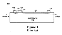
- Figure 1 shows an example of a transistor with ESD protection.
- the transistor 100 of Figure 1 includes a source region 140 formed in a substrate 110, a source contact 145, a gate 130 formed on a dielectric material 135. a drain region 120 formed in the substrate 110, and a drain contact 125.
- the drain region 120 is made large in order to prevent current crowding. Current crowding during an ESD event may cause a large current to focus on a small area of semiconductor material and thus cause damage to the device. By increasing the size of the drain region, the current during an ESD event is less likely to focus on a small area, thereby reducing the likelihood of damage to the device.
- the output drain capacitance is largely a function of drain region arca and depletion region width at the p-n junction formed by the substrate 110 and the drain region 120.
- WO-A-9631907 discloses a transistor with ESD protection similar to that described with reference to Figure 1 but which also includes a N-well in the drain region so as to prevent a short circuit from forming between the drain contact and the P substrate during a ESD-stress-induced contact spiking event.
- the document EP-A-0 387 944 discloses an integrated circuit with two transistors and an ESD protection element.
- the protection element comprises a gate, a gate dielectric underneath the gate, a p-type region underneath the gate dielectric and first and second n-type regions laterally adjacent to the p-type region.
- the first n-type region is about 10 ⁇ m long and is embedded in an n-type well region which extends between a portion of the first n-type region and the substrate.
- FIG. 2 depicts a transistor 200 embodying a technique used to reduce the output drain capacitance while maintaining ESD protection properties.
- the transistor 200 includes a source region 240 formed in a substrate 210, a source contact 245, a gate 230 formed over a dielectric material 235, a first drain region 220 formed in the substrate 210, a resistive region 215 formed in the substrate 210, a second drain region 227 formed in the substrate 210, and a drain contact 225 formed on the second drain region 227.
- the resistive region 215 provides the ESD protection.
- the resistive region 215 is of the same conductivity type as the first and second drain regions 220 and 227, but is more lightly doped.
- the depletion region width at the p-n junction formed by the substrate 210 and the resistive region 215 is much greater that the depletion region width achieved by the transistor 100 of Figure 1 .
- the increase in depletion region width results in a decrease in capacitance while maintaining ESD protection characteristics.
- transistors 100 and 200 require different steps during the fabrication process.
- the formation of the transistor 200 requires that the resistive region 215 be forme then a mask to be formed over the resistive region 215 during the formation of the source region 240 and drain regions 220 and 227.
- Many processes that fabricate transistor structures similar to that of the transistor 100 depicted in Figure 1 typically do not readily posses the ability to form the structure shown in Figure 2 due to the extra steps involved in masking the resistive region during formation of the source and drain regions. Consequently, while some processes are able to take advantage of the capacitance reduction using the structure shown in Figure 2 . many are not. For these reasons, a reduced-capacitance transistor with ESD protection that can be fabricated without significant additional processing is desirable.
- a reduced-capacitance transistor with ESD protection formed using standard fabrication processes is disclosed.
- specific details are set forth to provide a thorough understanding of the invention. However, it will be apparent to one skilled in the art that these specific details are not required to practice the invention. In other instances, well known methods, devices, and structures are not described in particular detail in order to avoid obscuring the invention.
- a transistor is formed including a substrate, a source region formed in the substrate, a gate structure defining a channel region in the substrate, and a well region also formed in the substrate.
- the transistor further includes a drain region formed at least partially in the well region.
- the well region is of the same semiconductor type as the source and drain regions, but is more lightly doped than the source and drain regions.
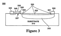
- FIG. 3 illustrates an example embodiment of a reduced-capacitance transistor 300 with ESD protection formed using standard fabrication processes and implemented in accordance with the invention.
- the transistor 300 includes a substrate 310, a source region 340 formed in the substrate, a gate structure including a gate contact 330 formed on a dielectric material 335 which is formed on the substrate, and a drain region 320 which includes a first end region 321, a second end region 322, and a resistive region 323 located between the first end region 321 and the second end region 322.
- the gate contact 330 and the dielectric material 335 define a channel region 337 in the substrate 310.
- the substrate 310 is formed of p- type semiconductor material, while the source region 340 and the drain region 320 are formed of n+ type semiconductor material.
- P type semiconductor material is typically formed by introducing a dopant such as boron into silicon.
- N type semiconductor material is typically formed by introducing a dopant such as arsenic into silicon. Other dopants are possible. Diffusion and ion implantation are two recognized methods of introducing dopants into silicon.
- the symbol “-” following "p” or “n” as used herein indicates that the "p” or "n” type semiconductor material is lightly doped.
- the symbol “+” following "p” or “n” as used herein indicates that the "p” or "n” type semiconductor material is heavily doped.
- a source contact 345 is formed on the source region 340 and a drain contact 325 is formed on the first end region 321 of the drain region 320.
- the source contact 345, the drain contact 325, and the gate contact 330 are preferably formed of polysilicon, although other electrically conductive materials may be used.
- the dielectric material 335 is preferably silicon dioxide. Other dielectric materials may also be used.
- the present example transistor has a gate length of preferably .25 micron ( ⁇ ), although a broad range of other dimensions are possible. For example, the invention may be practiced with a gate length of .1 ⁇ .
- the drain region is preferably formed to a depth of approximately .3 ⁇ using ion-implantation, but other depths are possible and any method for introducing dopants into a semiconductor material may be used to form the drain region.
- the resistive region 323 within the drain region 320 serves as an ESD protection structure.
- Enhanced ESD protection is achieved by increasing the size of the drain region 320 by inclusion of the resistive region 323.
- the resistive region has a length of preferably approximately 5 ⁇ . A broad range of other lengths are possible.
- the potentially large current is spread out over a greater area instead of focusing on a small area.
- This technique of providing ESD protection is discussed above in the background section.
- the capacitance between the large drain region and the substrate would be large compared to transistors with smaller drain regions.
- the invention reduces this capacitance by introducing a well region 315 between at least a portion of the drain region 320 and the substrate 310.
- the well region 315 is formed using standard well fabrication techniques that are well known in the art. Most semiconductor fabrication processes use wells. Consequently, the well region 315 can be formed during the normal well fabrication process, and no significant extra processing is required.
- the well region 315 is formed before the formation of the drain region 320.
- the well region 315 in this example embodiment is formed of n- type semiconductor material.
- the n- type semiconductor material for the well region 315 is preferably formed by defusing a dopant such as phosphorus into the silicon substrate, although other dopants are possible.
- the well region 315 may also be formed by ion-implantation or any other method for introducing dopants into a semiconductor material.
- the well region 315 is formed to a depth of preferably 3 ⁇ beneath the drain region 320 and is formed to extend from beneath the drain contact 325 to within 1 ⁇ of the channel region 337.
- the invention may be practiced using a broad range of well region depths.
- the well region 315 extends to within 1 ⁇ of the channel region.
- the substrate 310 is mentioned as being formed of a p type semiconductor material and the source 340, drain 320, and well 315 regions are mentioned as being formed of n type semiconductor material.
- the invention may also be practiced with an n type substrate and p type source, drain, and well regions.
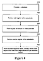
- FIG. 4 is a flow diagram of an example method for forming a reduced-capacitance transistor with ESD protection using standard fabrication processes and implemented in accordance with the invention.
- a substrate is provided.
- the substrate may have any of the properties discussed above in connection with Figure 3 .
- a well region is formed in the substrate.
- a gate structure is formed on the substrate. Once the gate structure is formed, a source region is formed in the substrate at step 440.
- a drain region, including a resistive region is formed. The drain region is formed at least partially in the well region.
- the properties of the substrate, source region, drain region, and well region provided or formed in steps 410, 420, 430, 440, and 450 conform to the properties for these structures as discussed above in connection with Figure 3 .
Landscapes
- Semiconductor Integrated Circuits (AREA)
- Metal-Oxide And Bipolar Metal-Oxide Semiconductor Integrated Circuits (AREA)
- Insulated Gate Type Field-Effect Transistor (AREA)
Applications Claiming Priority (3)
| Application Number | Priority Date | Filing Date | Title |
|---|---|---|---|
| US08/993,441 US5847431A (en) | 1997-12-18 | 1997-12-18 | Reduced capacitance transistor with electro-static discharge protection structure |
| US993441 | 1997-12-18 | ||
| PCT/US1998/022754 WO1999031729A1 (en) | 1997-12-18 | 1998-10-27 | Reduced capacitance transistor with electro-static discharge protection structure and method for forming the same |
Publications (3)
| Publication Number | Publication Date |
|---|---|
| EP1042808A1 EP1042808A1 (en) | 2000-10-11 |
| EP1042808A4 EP1042808A4 (en) | 2001-02-07 |
| EP1042808B1 true EP1042808B1 (en) | 2008-07-30 |
Family
ID=25539554
Family Applications (1)
| Application Number | Title | Priority Date | Filing Date |
|---|---|---|---|
| EP98955143A Expired - Lifetime EP1042808B1 (en) | 1997-12-18 | 1998-10-27 | Reduced capacitance transistor with electro-static discharge protection structure and method for forming the same |
Country Status (7)
| Country | Link |
|---|---|
| US (1) | US5847431A (enExample) |
| EP (1) | EP1042808B1 (enExample) |
| JP (1) | JP2002509358A (enExample) |
| KR (2) | KR100477950B1 (enExample) |
| CN (1) | CN1143387C (enExample) |
| AU (1) | AU1202199A (enExample) |
| WO (1) | WO1999031729A1 (enExample) |
Families Citing this family (2)
| Publication number | Priority date | Publication date | Assignee | Title |
|---|---|---|---|---|
| US6534867B1 (en) * | 1999-09-27 | 2003-03-18 | Kabushiki Kaisha Toshiba | Semiconductor device, semiconductor element and method for producing same |
| CN106158832A (zh) * | 2015-04-01 | 2016-11-23 | 联华电子股份有限公司 | 半导体结构 |
Family Cites Families (18)
| Publication number | Priority date | Publication date | Assignee | Title |
|---|---|---|---|---|
| US3876480A (en) * | 1972-08-28 | 1975-04-08 | Motorola Inc | Method of manufacturing high speed, isolated integrated circuit |
| US4684967A (en) * | 1984-05-04 | 1987-08-04 | Integrated Logic Systems, Inc. | Low capacitance transistor cell element and transistor array |
| JPS6153761A (ja) * | 1984-08-24 | 1986-03-17 | Hitachi Ltd | 半導体装置 |
| FR2598852B1 (fr) * | 1986-05-16 | 1988-10-21 | Eurotechnique Sa | Dispositif de protection d'entree pour circuits integres en technologie cmos. |
| NL8900593A (nl) * | 1989-03-13 | 1990-10-01 | Philips Nv | Halfgeleiderinrichting met een beveiligingsschakeling. |
| US5121179A (en) * | 1990-10-08 | 1992-06-09 | Seiko Epson Corporation | Higher impedance pull-up and pull-down input protection resistors for MIS transistor integrated circuits |
| JPH03174763A (ja) * | 1989-12-04 | 1991-07-29 | Hitachi Ltd | 半導体装置 |
| FR2685817B1 (fr) * | 1991-12-31 | 1994-03-11 | Sgs Thomson Microelectronics Sa | Protection generale d'un circuit integre contre les surcharges permanentes et decharges electrostatiques. |
| DE4334515C1 (de) * | 1993-10-09 | 1994-10-20 | Itt Ind Gmbh Deutsche | Verpolungsschutz für integrierte elektronische Schaltkreise in CMOS-Technik |
| JP3493713B2 (ja) * | 1994-03-04 | 2004-02-03 | 松下電器産業株式会社 | 半導体装置 |
| JPH07321303A (ja) * | 1994-05-19 | 1995-12-08 | Kobe Steel Ltd | Mos型半導体装置及びその製造方法 |
| JP3332123B2 (ja) * | 1994-11-10 | 2002-10-07 | 株式会社東芝 | 入力保護回路及びこれを用いた半導体装置 |
| US5485025A (en) * | 1994-12-02 | 1996-01-16 | Texas Instruments Incorporated | Depleted extrinsic emitter of collector-up heterojunction bipolar transistor |
| CN1099713C (zh) * | 1995-04-06 | 2003-01-22 | 工业技术研究院 | 用n边多边形单元布线的mos单元、多单元晶体管及ic芯片 |
| JPH0936357A (ja) * | 1995-07-18 | 1997-02-07 | Matsushita Electric Ind Co Ltd | 半導体装置 |
| US5623156A (en) * | 1995-09-28 | 1997-04-22 | Cypress Semiconductor Corporation | Electrostatic discharge (ESD) protection circuit and structure for output drivers |
| KR100190008B1 (ko) * | 1995-12-30 | 1999-06-01 | 윤종용 | 반도체 장치의 정전하 보호 장치 |
| US5623787A (en) * | 1996-01-05 | 1997-04-29 | Ali; Elsayed A. | Tile roof valley guard |
-
1997
- 1997-12-18 US US08/993,441 patent/US5847431A/en not_active Expired - Lifetime
-
1998
- 1998-10-27 WO PCT/US1998/022754 patent/WO1999031729A1/en not_active Ceased
- 1998-10-27 CN CNB988123843A patent/CN1143387C/zh not_active Expired - Fee Related
- 1998-10-27 EP EP98955143A patent/EP1042808B1/en not_active Expired - Lifetime
- 1998-10-27 KR KR10-2003-7007165A patent/KR100477950B1/ko not_active Expired - Fee Related
- 1998-10-27 JP JP2000539527A patent/JP2002509358A/ja active Pending
- 1998-10-27 AU AU12021/99A patent/AU1202199A/en not_active Abandoned
- 1998-10-27 KR KR10-2000-7006497A patent/KR100395345B1/ko not_active Expired - Fee Related
Also Published As
| Publication number | Publication date |
|---|---|
| KR100477950B1 (ko) | 2005-03-22 |
| CN1143387C (zh) | 2004-03-24 |
| EP1042808A4 (en) | 2001-02-07 |
| KR20010033125A (ko) | 2001-04-25 |
| EP1042808A1 (en) | 2000-10-11 |
| CN1282449A (zh) | 2001-01-31 |
| JP2002509358A (ja) | 2002-03-26 |
| KR20030048485A (ko) | 2003-06-19 |
| AU1202199A (en) | 1999-07-05 |
| US5847431A (en) | 1998-12-08 |
| WO1999031729A1 (en) | 1999-06-24 |
| KR100395345B1 (ko) | 2003-08-21 |
Similar Documents
| Publication | Publication Date | Title |
|---|---|---|
| EP0452829B1 (en) | Semiconductor device with reduced time-dependent dielectric failures | |
| US6396102B1 (en) | Field coupled power MOSFET bus architecture using trench technology | |
| KR100389768B1 (ko) | 정전기방전보호구조를가진반도체장치및형성방법 | |
| KR100816253B1 (ko) | 트렌치 게이트 전계 효과 트랜지스터 및 그의 제조 방법 | |
| JP3066001B2 (ja) | 拡散抵抗デバイス及び埋め込みコンデンサを形成する方法 | |
| EP0874397A2 (en) | Parasitic isolation transistor having an adjustable threshold voltage | |
| US5903032A (en) | Power device integration for built-in ESD robustness | |
| JP2000101084A (ja) | 空乏ポリシリコン・エッジ型mosfet構造及び方法 | |
| JP2004528719A5 (enExample) | ||
| EP0680090B1 (en) | Protection device against electrostatic discharges | |
| US6631060B2 (en) | Field oxide device with zener junction for electrostatic discharge (ESD) protection and other applications | |
| US6501155B2 (en) | Semiconductor apparatus and process for manufacturing the same | |
| US5604369A (en) | ESD protection device for high voltage CMOS applications | |
| US8093121B1 (en) | ESD protection transistor | |
| US6114731A (en) | Low capacitance ESD structure having a source inside a well and the bottom portion of the drain inside a substrate | |
| EP1042808B1 (en) | Reduced capacitance transistor with electro-static discharge protection structure and method for forming the same | |
| US6049112A (en) | Reduced capacitance transistor with electro-static discharge protection structure and method for forming the same | |
| US6281553B1 (en) | Semiconductor device, electrostatic discharge protection device, and dielectric breakdown preventing method | |
| US4890143A (en) | Protective clamp for MOS gated devices | |
| US6461922B1 (en) | Method for the integration of resistors and esd self-protected transistors in an integrated device with a memory matrix manufactured by means of a process featuring self-aligned source (sas) formation and junction salicidation | |
| JPS6359258B2 (enExample) | ||
| JPH10313113A (ja) | 半導体装置 |
Legal Events
| Date | Code | Title | Description |
|---|---|---|---|
| PUAI | Public reference made under article 153(3) epc to a published international application that has entered the european phase |
Free format text: ORIGINAL CODE: 0009012 |
|
| 17P | Request for examination filed |
Effective date: 20000619 |
|
| AK | Designated contracting states |
Kind code of ref document: A1 Designated state(s): GB IE |
|
| A4 | Supplementary search report drawn up and despatched |
Effective date: 20001227 |
|
| AK | Designated contracting states |
Kind code of ref document: A4 Designated state(s): GB IE |
|
| RIC1 | Information provided on ipc code assigned before grant |
Free format text: 7H 01L 23/62 A, 7H 01L 29/788 B, 7H 01L 27/02 B |
|
| 17Q | First examination report despatched |
Effective date: 20030902 |
|
| GRAP | Despatch of communication of intention to grant a patent |
Free format text: ORIGINAL CODE: EPIDOSNIGR1 |
|
| GRAS | Grant fee paid |
Free format text: ORIGINAL CODE: EPIDOSNIGR3 |
|
| GRAA | (expected) grant |
Free format text: ORIGINAL CODE: 0009210 |
|
| AK | Designated contracting states |
Kind code of ref document: B1 Designated state(s): GB IE |
|
| REG | Reference to a national code |
Ref country code: GB Ref legal event code: FG4D |
|
| REG | Reference to a national code |
Ref country code: IE Ref legal event code: FG4D |
|
| PLBE | No opposition filed within time limit |
Free format text: ORIGINAL CODE: 0009261 |
|
| STAA | Information on the status of an ep patent application or granted ep patent |
Free format text: STATUS: NO OPPOSITION FILED WITHIN TIME LIMIT |
|
| 26N | No opposition filed |
Effective date: 20090506 |
|
| REG | Reference to a national code |
Ref country code: IE Ref legal event code: MM4A |
|
| PG25 | Lapsed in a contracting state [announced via postgrant information from national office to epo] |
Ref country code: IE Free format text: LAPSE BECAUSE OF NON-PAYMENT OF DUE FEES Effective date: 20081027 |
|
| PGFP | Annual fee paid to national office [announced via postgrant information from national office to epo] |
Ref country code: GB Payment date: 20120111 Year of fee payment: 14 |
|
| GBPC | Gb: european patent ceased through non-payment of renewal fee |
Effective date: 20121027 |
|
| PG25 | Lapsed in a contracting state [announced via postgrant information from national office to epo] |
Ref country code: GB Free format text: LAPSE BECAUSE OF NON-PAYMENT OF DUE FEES Effective date: 20121027 |