EP1032049B1 - Photoelectric converting element - Google Patents
Photoelectric converting element Download PDFInfo
- Publication number
- EP1032049B1 EP1032049B1 EP00301461A EP00301461A EP1032049B1 EP 1032049 B1 EP1032049 B1 EP 1032049B1 EP 00301461 A EP00301461 A EP 00301461A EP 00301461 A EP00301461 A EP 00301461A EP 1032049 B1 EP1032049 B1 EP 1032049B1
- Authority
- EP
- European Patent Office
- Prior art keywords
- region
- type
- electrode
- light
- semiconductor
- Prior art date
- Legal status (The legal status is an assumption and is not a legal conclusion. Google has not performed a legal analysis and makes no representation as to the accuracy of the status listed.)
- Expired - Lifetime
Links
- 239000004065 semiconductor Substances 0.000 claims description 190
- 239000012535 impurity Substances 0.000 claims description 64
- 239000004020 conductor Substances 0.000 claims description 7
- 230000003247 decreasing effect Effects 0.000 claims description 7
- 239000000758 substrate Substances 0.000 description 68
- 238000006243 chemical reaction Methods 0.000 description 30
- 238000000034 method Methods 0.000 description 22
- 230000000779 depleting effect Effects 0.000 description 21
- 230000007547 defect Effects 0.000 description 20
- 229910052751 metal Inorganic materials 0.000 description 20
- 239000002184 metal Substances 0.000 description 20
- 230000002829 reductive effect Effects 0.000 description 17
- 239000013078 crystal Substances 0.000 description 15
- 239000000969 carrier Substances 0.000 description 12
- 230000002441 reversible effect Effects 0.000 description 12
- 238000005468 ion implantation Methods 0.000 description 11
- 230000035945 sensitivity Effects 0.000 description 11
- 238000010586 diagram Methods 0.000 description 9
- 238000005530 etching Methods 0.000 description 9
- 229920002120 photoresistant polymer Polymers 0.000 description 9
- 238000007669 thermal treatment Methods 0.000 description 8
- 238000002955 isolation Methods 0.000 description 7
- 230000015572 biosynthetic process Effects 0.000 description 6
- 150000002500 ions Chemical class 0.000 description 6
- 230000014759 maintenance of location Effects 0.000 description 6
- 239000000463 material Substances 0.000 description 6
- 239000007787 solid Substances 0.000 description 6
- 230000008569 process Effects 0.000 description 5
- 238000003860 storage Methods 0.000 description 5
- 108091006146 Channels Proteins 0.000 description 4
- 238000004380 ashing Methods 0.000 description 4
- 230000015556 catabolic process Effects 0.000 description 4
- 230000008859 change Effects 0.000 description 4
- 230000005684 electric field Effects 0.000 description 4
- 230000003647 oxidation Effects 0.000 description 4
- 238000007254 oxidation reaction Methods 0.000 description 4
- 238000000206 photolithography Methods 0.000 description 4
- 230000000740 bleeding effect Effects 0.000 description 3
- 230000007423 decrease Effects 0.000 description 3
- 238000004519 manufacturing process Methods 0.000 description 3
- 230000007935 neutral effect Effects 0.000 description 3
- 230000003287 optical effect Effects 0.000 description 3
- 230000001590 oxidative effect Effects 0.000 description 3
- 238000005036 potential barrier Methods 0.000 description 3
- 230000001681 protective effect Effects 0.000 description 3
- ZOXJGFHDIHLPTG-UHFFFAOYSA-N Boron Chemical compound [B] ZOXJGFHDIHLPTG-UHFFFAOYSA-N 0.000 description 2
- 229910052581 Si3N4 Inorganic materials 0.000 description 2
- VYPSYNLAJGMNEJ-UHFFFAOYSA-N Silicium dioxide Chemical compound O=[Si]=O VYPSYNLAJGMNEJ-UHFFFAOYSA-N 0.000 description 2
- ATJFFYVFTNAWJD-UHFFFAOYSA-N Tin Chemical compound [Sn] ATJFFYVFTNAWJD-UHFFFAOYSA-N 0.000 description 2
- 229910052782 aluminium Inorganic materials 0.000 description 2
- 229910052796 boron Inorganic materials 0.000 description 2
- 238000009826 distribution Methods 0.000 description 2
- 230000006870 function Effects 0.000 description 2
- 231100000989 no adverse effect Toxicity 0.000 description 2
- 238000001020 plasma etching Methods 0.000 description 2
- 229910021420 polycrystalline silicon Inorganic materials 0.000 description 2
- 229920005591 polysilicon Polymers 0.000 description 2
- 230000005855 radiation Effects 0.000 description 2
- 229910052710 silicon Inorganic materials 0.000 description 2
- 239000010703 silicon Substances 0.000 description 2
- HQVNEWCFYHHQES-UHFFFAOYSA-N silicon nitride Chemical compound N12[Si]34N5[Si]62N3[Si]51N64 HQVNEWCFYHHQES-UHFFFAOYSA-N 0.000 description 2
- 229910052814 silicon oxide Inorganic materials 0.000 description 2
- 229910052718 tin Inorganic materials 0.000 description 2
- 229910000838 Al alloy Inorganic materials 0.000 description 1
- 229910018182 Al—Cu Inorganic materials 0.000 description 1
- 229910015844 BCl3 Inorganic materials 0.000 description 1
- 229910000531 Co alloy Inorganic materials 0.000 description 1
- 229910000599 Cr alloy Inorganic materials 0.000 description 1
- 229910000881 Cu alloy Inorganic materials 0.000 description 1
- 229910001182 Mo alloy Inorganic materials 0.000 description 1
- 108010075750 P-Type Calcium Channels Proteins 0.000 description 1
- OAICVXFJPJFONN-UHFFFAOYSA-N Phosphorus Chemical compound [P] OAICVXFJPJFONN-UHFFFAOYSA-N 0.000 description 1
- 229910001362 Ta alloys Inorganic materials 0.000 description 1
- 229910004166 TaN Inorganic materials 0.000 description 1
- 229910001069 Ti alloy Inorganic materials 0.000 description 1
- 229910001080 W alloy Inorganic materials 0.000 description 1
- 229910045601 alloy Inorganic materials 0.000 description 1
- 239000000956 alloy Substances 0.000 description 1
- XAGFODPZIPBFFR-UHFFFAOYSA-N aluminium Chemical compound [Al] XAGFODPZIPBFFR-UHFFFAOYSA-N 0.000 description 1
- 229910052785 arsenic Inorganic materials 0.000 description 1
- RQNWIZPPADIBDY-UHFFFAOYSA-N arsenic atom Chemical compound [As] RQNWIZPPADIBDY-UHFFFAOYSA-N 0.000 description 1
- 230000004888 barrier function Effects 0.000 description 1
- 239000005380 borophosphosilicate glass Substances 0.000 description 1
- 239000003990 capacitor Substances 0.000 description 1
- 239000002800 charge carrier Substances 0.000 description 1
- 229910052804 chromium Inorganic materials 0.000 description 1
- 239000011248 coating agent Substances 0.000 description 1
- 238000000576 coating method Methods 0.000 description 1
- 150000001875 compounds Chemical class 0.000 description 1
- 229910052802 copper Inorganic materials 0.000 description 1
- 230000001419 dependent effect Effects 0.000 description 1
- 238000009792 diffusion process Methods 0.000 description 1
- 239000002019 doping agent Substances 0.000 description 1
- 238000001312 dry etching Methods 0.000 description 1
- 230000000694 effects Effects 0.000 description 1
- 238000005516 engineering process Methods 0.000 description 1
- 150000002739 metals Chemical class 0.000 description 1
- 238000012986 modification Methods 0.000 description 1
- 230000004048 modification Effects 0.000 description 1
- 229910052750 molybdenum Inorganic materials 0.000 description 1
- 150000004767 nitrides Chemical class 0.000 description 1
- 230000003071 parasitic effect Effects 0.000 description 1
- 238000000059 patterning Methods 0.000 description 1
- 229910052698 phosphorus Inorganic materials 0.000 description 1
- 239000011574 phosphorus Substances 0.000 description 1
- 230000002265 prevention Effects 0.000 description 1
- 229920006395 saturated elastomer Polymers 0.000 description 1
- 238000004544 sputter deposition Methods 0.000 description 1
- 239000007858 starting material Substances 0.000 description 1
- 230000001629 suppression Effects 0.000 description 1
- 229910052715 tantalum Inorganic materials 0.000 description 1
- 229910052719 titanium Inorganic materials 0.000 description 1
- 230000007704 transition Effects 0.000 description 1
- FAQYAMRNWDIXMY-UHFFFAOYSA-N trichloroborane Chemical compound ClB(Cl)Cl FAQYAMRNWDIXMY-UHFFFAOYSA-N 0.000 description 1
- 229910052721 tungsten Inorganic materials 0.000 description 1
Images


Classifications
-
- H—ELECTRICITY
- H01—ELECTRIC ELEMENTS
- H01L—SEMICONDUCTOR DEVICES NOT COVERED BY CLASS H10
- H01L27/00—Devices consisting of a plurality of semiconductor or other solid-state components formed in or on a common substrate
- H01L27/14—Devices consisting of a plurality of semiconductor or other solid-state components formed in or on a common substrate including semiconductor components sensitive to infrared radiation, light, electromagnetic radiation of shorter wavelength or corpuscular radiation and specially adapted either for the conversion of the energy of such radiation into electrical energy or for the control of electrical energy by such radiation
- H01L27/144—Devices controlled by radiation
- H01L27/146—Imager structures
- H01L27/14601—Structural or functional details thereof
- H01L27/14603—Special geometry or disposition of pixel-elements, address-lines or gate-electrodes
-
- H—ELECTRICITY
- H01—ELECTRIC ELEMENTS
- H01L—SEMICONDUCTOR DEVICES NOT COVERED BY CLASS H10
- H01L31/00—Semiconductor devices sensitive to infrared radiation, light, electromagnetic radiation of shorter wavelength or corpuscular radiation and specially adapted either for the conversion of the energy of such radiation into electrical energy or for the control of electrical energy by such radiation; Processes or apparatus specially adapted for the manufacture or treatment thereof or of parts thereof; Details thereof
- H01L31/0248—Semiconductor devices sensitive to infrared radiation, light, electromagnetic radiation of shorter wavelength or corpuscular radiation and specially adapted either for the conversion of the energy of such radiation into electrical energy or for the control of electrical energy by such radiation; Processes or apparatus specially adapted for the manufacture or treatment thereof or of parts thereof; Details thereof characterised by their semiconductor bodies
- H01L31/0352—Semiconductor devices sensitive to infrared radiation, light, electromagnetic radiation of shorter wavelength or corpuscular radiation and specially adapted either for the conversion of the energy of such radiation into electrical energy or for the control of electrical energy by such radiation; Processes or apparatus specially adapted for the manufacture or treatment thereof or of parts thereof; Details thereof characterised by their semiconductor bodies characterised by their shape or by the shapes, relative sizes or disposition of the semiconductor regions
-
- H—ELECTRICITY
- H01—ELECTRIC ELEMENTS
- H01L—SEMICONDUCTOR DEVICES NOT COVERED BY CLASS H10
- H01L31/00—Semiconductor devices sensitive to infrared radiation, light, electromagnetic radiation of shorter wavelength or corpuscular radiation and specially adapted either for the conversion of the energy of such radiation into electrical energy or for the control of electrical energy by such radiation; Processes or apparatus specially adapted for the manufacture or treatment thereof or of parts thereof; Details thereof
- H01L31/08—Semiconductor devices sensitive to infrared radiation, light, electromagnetic radiation of shorter wavelength or corpuscular radiation and specially adapted either for the conversion of the energy of such radiation into electrical energy or for the control of electrical energy by such radiation; Processes or apparatus specially adapted for the manufacture or treatment thereof or of parts thereof; Details thereof in which radiation controls flow of current through the device, e.g. photoresistors
- H01L31/10—Semiconductor devices sensitive to infrared radiation, light, electromagnetic radiation of shorter wavelength or corpuscular radiation and specially adapted either for the conversion of the energy of such radiation into electrical energy or for the control of electrical energy by such radiation; Processes or apparatus specially adapted for the manufacture or treatment thereof or of parts thereof; Details thereof in which radiation controls flow of current through the device, e.g. photoresistors characterised by at least one potential-jump barrier or surface barrier, e.g. phototransistors
- H01L31/101—Devices sensitive to infrared, visible or ultraviolet radiation
- H01L31/102—Devices sensitive to infrared, visible or ultraviolet radiation characterised by only one potential barrier or surface barrier
- H01L31/103—Devices sensitive to infrared, visible or ultraviolet radiation characterised by only one potential barrier or surface barrier the potential barrier being of the PN homojunction type
-
- Y—GENERAL TAGGING OF NEW TECHNOLOGICAL DEVELOPMENTS; GENERAL TAGGING OF CROSS-SECTIONAL TECHNOLOGIES SPANNING OVER SEVERAL SECTIONS OF THE IPC; TECHNICAL SUBJECTS COVERED BY FORMER USPC CROSS-REFERENCE ART COLLECTIONS [XRACs] AND DIGESTS
- Y02—TECHNOLOGIES OR APPLICATIONS FOR MITIGATION OR ADAPTATION AGAINST CLIMATE CHANGE
- Y02E—REDUCTION OF GREENHOUSE GAS [GHG] EMISSIONS, RELATED TO ENERGY GENERATION, TRANSMISSION OR DISTRIBUTION
- Y02E10/00—Energy generation through renewable energy sources
- Y02E10/50—Photovoltaic [PV] energy
- Y02E10/547—Monocrystalline silicon PV cells
Definitions
- the present invention relates to a photoelectric converting element of an image sensor used for such an image-reading system as a digital camera, an image scanner, a facsimile, a copying machine, etc., as well as a photoelectric conversion device comprising the photoelectric converting element, specifically to the structure of a photoelectric converting element suitable for a photoelectric conversion device such as a close contact type image sensor, which is provided with a comparatively large photoelectric converting element having the opening portion of a pixel with several tens microns or more in size.
- Document US 4,652,899 discloses a radiation-sensitive semiconductor device having a reduced capacitance.
- the capacitance of a radiation-sensitive diode can be considerably reduced by giving it the form of a pn junction (4) between a first semiconductor region (4) and a layer-shaped semiconductor zone, which in operation is fully depleted.
- the speed of such a diode is favorably influenced by the choice or the shape of the geometry of the layer-shaped zone. When the latter is formed with parts decreasing in width of thickness, an electric field is produced in these parts which accelerates the transport of minority charge carriers to a central contact.
- document EP 0 854 516 A2 discloses a partially pinned photodiode for solid state image sensors.
- a pixelated image sensor comprising a partially pinned photodiode which is formed a semiconductor of a first conductivity type formed on a surface of the sensor with at least one photodiode formed within the semiconductor near the surface is disclosed.
- the photodiode being formed from a second conductivity type opposite the first conductivity type; a pinning layer formed on the surface over at least a portion of the photodiode creating a pinned photodiode region, the pinning layer being formed from the first conductivity type; an unpinned region formed near the surface in an area outside the portion used to form the pinning layer, and the unpinned region is formed as a floating region that is employed as a capacitor.
- the partially pinned photodiode is useful in expanding the fill factor of photodetectors employing photodiode technology.
- document US 5,514,887 discloses a solid state image sensor having a high photoelectric conversion efficiency.
- the impurity layer is composed of a first impurity region formed of a low concentration at a deep level, and a second impurity region formed of a high concentration at a shallow level.
- the first impurity region extends under a second impurity layer of a second conductivity type formed for device isolation, and also extends under a gate region of a transistor for transferring an electric charge from the photodiode to a CCD channel.
- CCD image sensors In recent years, CCD image sensors, non-CCD image sensors such as CMOS image sensors, etc. have been positively developed as photoelectric conversion devices.
- a photodiode comprising a PN junction of a semiconductor is used for light-receiving elements of these photoelectric conversion devices.
- a structure of a light-receiving element in which the surface of a substrate where no PN junction is formed has a region having the same conductivity type as that of the substrate and a larger impurity concentration than that of the substrate, thereby reducing the dark current to be generated on the surface of the substrate.
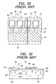
- Figs. 29A and 29B show a structure of a conventional light-receiving element.
- Numeral 201 indicates an n-type semiconductor substrate; 202: a p-type semiconductor layer; 203: an n-type semiconductor layer having an impurity concentration of 5 ⁇ 10 15 cm -3 to 10 ⁇ 10 15 cm -3 and a thickness of 0.2 ⁇ m to 0.3 ⁇ m; 205: a thermal oxide film; 208: an n + channel stopper; 209: an anti-reflection coating film consisting of nitride; 215 and 216: aluminum electrodes; 228: an n + -type semiconductor layer; and 238: a surface electrode.
- Symbol DL indicates a depletion layer; and DLS: a surface side portion of the depletion layer.
- the anode of a photodiode is formed only with a p-type semiconductor layer 202.
- the impurity concentration is lowered, therefore, the property of the ohmic contact with the electrode 215 is degraded.
- the impurity concentration is increased, the depletion layer DL is not extended into the semiconductor layer 202.
- Fig. 30 shows a top view of a conventional photoelectric conversion device such as a CCD image sensor.
- Numeral 301 indicates a p-type substrate and numeral 302 indicates an n + -type accumulating portion.
- a portion surrounded by the n + -type accumulating portion 302 on the p-type substrate 301 is a p-type photoelectric conversion region functioning as a pixel.
- Symbol PG indicates a photo-gate; SG: a shift-gate; and SR: a CCD shift-register.
- the PN junction area is reduced, but the PN junction periphery length is increased. It is therefore impossible to sufficiently reduce the capacitance of the PN junction, whereby the sensitivity cannot be increased so much.
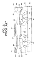
- Fig. 31 shows a cross-sectional view of a light-receiving element of prior art.
- numeral 301 indicates a P-type semiconductor region; 302: an N-type semiconductor region; 303: a P-type shallow channel stop layer; 305: a field oxide film; 306: a P-type substrate; 308: a P-type channel stop layer; 309: an interlayered insulating film; 317 :a light-shielding film for forming an opening portion (OP).
- a depletion layer (DL) is extended into the P-type semiconductor region 301, whereby electrons of the generated photocarriers (PC) are collected in the N-type semiconductor region 302 by to an internal magnetic field.
- a photodiode having a cross-sectional structure of N-type substrate/P-type region/N-type region/P-type region is generally used as a light-receiving element of a CCD image sensor.
- Fig. 32 shows a cross-sectional view of a light-receiving element of prior art.
- numeral 406 indicates an N-type substrate; 401: a P-type semiconductor region; 402: an N-type semiconductor region; 403: a shallow P-type semiconductor layer; 408: a P + -type channel stop layer; 409: an insulating film; 415: an electrode consisting of polysilicon; and 420: an N-type region of a CCD register.
- a photoelectric conversion device employing a light-receiving element is proposed, for example, in Japanese Patent Application Laid-Open No. 9-205588 , which uses a photodiode as a light-receiving element and reads the electric charges of the light-receiving element at a time with use of a source follower amplifier by providing this light-receiving element with an electrode and connecting it to the gate electrode of an MOS transistor.
- Fig. 33 is a cross-sectional view of a light-receiving element of prior art provided with an electrode.
- numeral 701 indicates a first semiconductor region
- numeral 702 indicates a second semiconductor region to be used as an anode.
- the conductivity types of those regions are N-type and P-type, respectively.
- symbol DL is a depletion layer formed by a PN junction between the first semiconductor region 701 and the second conductor region 702.
- a reverse bias is applied to between the first semiconductor region 701 and the second semiconductor region 702.
- numeral 715 indicates an electrode, which is connected to the second semiconductor region 702 through a contact hole CH of the insulating film 709.
- the electrode 715 is composed of a metal, for example, A1 as a main component.
- the electrode 715 is connected to an electrode region formed on the major surface of the semiconductor substrate through a contact hole CH of the insulating film covering the surface of the photodiode.
- such light-receiving element is composed by connecting a conductive material such as A1 to a semiconductor region so as to obtain photosignals generated by photocarriers photoelectric-converted in the semiconductor region.
- Crystal defects may also generate due to the plasma ashing of a photoresist, etc. even in a step after the electrode is formed, just like in the above case.
- a PN junction exists around a semiconductor region formed on the major surface of the semiconductor substrate to which an electrode is connected and the junction surface reaches the vicinity of the interface between the major surface of the semiconductor substrate and the insulating film in many cases.
- the generated dark current as described above also becomes a factor for causing the dark current to be varied, since the quantity of the crystal defects generated in the vicinity of the interface or the quantity of crystal defects themselves is changed by misalignment of a mask in formation of electrodes, etc. and etching conditions.
- the first object of the present invention is to provide a photoelectric converting element wherein photo-generated holes can be collected to the electrode region at high speed.
- Figs. 1A to 1D show most properly the characteristics of the first embodiment.
- Fig. 1A is a top view of a light-receiving element part in the first embodiment.
- Fig. 1B is a sectional view taken in the line 1B-1B of Fig. 1A.
- Fig. 1C is a potential profile view taken in the line 1C-1C of Fig. 1B.
- Fig. 1D is a potential profile view taken in the line 1D-1D of Fig. 1B .
- numerals 1, 2 and 3 respectively denote a first semiconductor region of a first conductivity type provided in a semiconductor substrate, a second semiconductor region of a second conductivity type provided in the first semiconductor region 1, and a third semiconductor region of the first conductivity type provided in the major surface side of the second semiconductor region 2.
- Numeral 4 denotes an electrode region provided adjacent to the second semiconductor region 2 to take out electric charges generated by light (hereinafter referred to as "photo-generated electric charges"). More specifically, the electrode region 4 is composed of a high impurity concentration region having the same conductivity type as that of the second semiconductor region 2 and having an impurity concentration higher than that of the second semiconductor region, or the like.
- Numeral 102 denotes a light-receiving region 102 composed of the first, second and third semiconductor regions 1, 2 and 3. Carriers generated in the region 102 by light incidence are captured in a region 101. Needless to say, when the light is incident on the region 101, the carriers will be generated in this region 101.
- the first conductivity type is shown as a p-type and the second conductivity type is shown as an n-type.
- the first conductivity type may be an n-type and the second conductivity type may be a p-type.
- an insulating film is formed on the surface of a semiconductor substrate, openings are formed on the insulating film, and conductors serving as electrodes are formed in the openings.
- carriers (electrons in this case) generated in the light-receiving region 102 move transversely as shown in Fig. 1C and the electrons are collected to the groove of potential, i.e., the region 4 whose potential is the lowest.
- Fig. 1D another feature resides in that the impurity concentration and the junction depth of the third semiconductor region 3 on the surface, the first semiconductor region 1 and the second semiconductor region 2 and the potential applied to the electrode region 4 and the region 1 are set so that the second semiconductor region 2 is depleted throughout a substantially entire area thereof. As a result, the second semiconductor region 2 hardly contributes to capacitance, so that the capacitance of the light-receiving portion can be reduced.
- the electrons generated in the vicinity of the junction interface of the region 2 and the region 1 are collected to the region 2 in accordance with a built-in potential due to the pn junction therebetween.
- the electrons generated in the vicinity of the junction interface of the region 2 and the region 3 are collected to the region 2 in accordance with a built-in potential due to the pn junction therebetween.
- the region 2 of the light-receiving region 102 is almost depleted due to the above described two pn junctions, a neutral region does not exist. This state is referred to as "full-depletion formation".
- the collected electrons are gathered to the region 4 as described above.
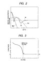
- Fig. 2 shows the distribution of the concentration of impurities in the direction along the line 1D-1D of Fig. 1B .
- Np1 denotes the concentration of p-type impurities such as boron in the p-type semiconductor substrate which is a starting material of the region 1.
- Nn1 denotes the concentration of n-type impurities such as phosphorus or arsenic introduced to form the region 2.
- Np2 denotes the concentration of p-type impurities introduced to form the region 3.
- NC denotes the net concentration (net value) of impurities in each region.
- the impurity concentration and the thickness of each region can be selected from the following ranges.
- the parameter of the thickness indicates a junction depth from the surface of the substrate.
- the impurity concentration ND1 of the first semiconductor region 1 is in a range of 10 14 cm -3 to 10 17 cm -3 , and more preferably in a range of 10 15 cm -3 to 10 16 cm -3 .
- the impurity concentration ND2 of the second semiconductor region 2 is in a range of 10 15 cm -3 to 10 18 cm -3 , and more preferably in a range of 10 16 cm -3 to 10 17 cm -3 , and the junction depth is in a range of 0.2 ⁇ m to 2 ⁇ m.
- the impurity concentration ND3 of the semiconductor region 3 is in a range of 10 16 cm -3 to 10 19 cm -3 , and more preferably in a range of 10 17 cm -3 to 10 18 cm -3 , and the junction depth is in a range of 0.1 ⁇ m to 0.5 ⁇ m.
- the impurity concentration ND4 of the electrode region 4 is in a range of 10 18 cm -3 to 10 21 cm -3 , and more preferably, in a range of 10 19 cm -3 to 10 20 cm -3 , and the junction depth ranges from 0.1 ⁇ m to 0.3 ⁇ m.
- Fig. 3 the relationship between the voltage of the electrode region 4 and a capacitance at that time is shown in Fig. 3 .
- the capacitance of the electrode region 4 becomes constant from a point A as a boundary.
- the region 2 When the voltage is low, the region 2 is not depleted and the capacitance changes depending on the capacitance component of a depletion layer between the region 2 and the region 3 and the capacitance component of a depletion layer between the region 2 and the region 1. In other words, as the capacitance of the region 4 rises, the depletion layer is more spread, so that the capacitance is gradually decreased.
- the region 2 in the light-receiving region 102 is almost fully depleted, hence, the capacitance is abruptly decreased, and then, becomes constant.
- the transition point thereof is indicated by the point A of Fig. 3 .
- the voltage in this point A is referred to as "depleting voltage".
- the depleting voltage is determined depending on the thickness and the impurity concentration of each region 1, 2 or 3
- (a) the potential of the electrode region 4 under a state in which the light-receiving element is reset and (b) the potential of the electrode region 4 under a state in which the optical output of the light-receiving element is saturated are set to this depletion voltage or higher, hence the capacitance of a photodiode itself can be substantially reduced to the junction capacitance (Co) or so on the bottom portion of the region 101 to realize a high sensitivity.
- an operating point (a range in which the potential changes) is designed so as to have the depletion voltage or higher, so that a photoelectric conversion characteristic with high sensitivity and good linearity can be obtained, because the capacitance of the electrode region 4 has a linearity.
- the capacitance value of a photodiode in which the electrode region 4 is not depleted is about 4400 times as large as the capacitance value of a photodiode in the case of the light-receiving element provided with the first region 1 having a thickness of approximately 600 ⁇ m and an impurity concentration of 1 ⁇ 10 16 cm -3 , the region 2 having a junction depth of 0.5 ⁇ m and an impurity concentration of 1 ⁇ 10 17 cm -3 , the region 3 having a junction depth of 0.2 ⁇ m and an impurity concentration of 1 ⁇ 10 18 cm -3 and the region 4 having a junction depth of 0.2 ⁇ m and an impurity concentration of 1 ⁇ 10 19 cm -3 , the region 2 having an upper surface with an area of 80 ⁇ m ⁇ 80 ⁇ m and the region 4 having an upper surface with an area of 1.2 ⁇ m ⁇ 1.2 ⁇ m.
- most of electrons generated within a distance of at least about 1 ⁇ m from the surface can be collected in any position of the light-receiving surface.
- most of blue light is absorbed within a range of 1 ⁇ m from the surface of silicon, the sensitivity to the blue light which is a problem of a visible light sensor is improved.
- a high energy ion implantation technique or the like is utilized to use such a retrograde well structure which has the peak value of the impurity concentration in the substrate, or, conversely, the concentration of the substrate 1 is lowered to widen the depletion layer so that the electrons generated in a deeper portion can be collected.
- an impurity layer with a high concentration is formed on the surface of the substrate, an epitaxial layer with a low impurity concentration is provided thereon, and the present invention is applied thereto, so that the structure of a light-receiving portion with a high sensitivity to a long wavelength can be obtained.
- Fig. 4 shows one example of a read and reset circuit employed in the present invention.
- D1 denotes a photodiode composed of a photoelectric converting element according to the present invention.
- M1 denotes a reset switch composed of an MOS transistor or the like.
- M2 denotes an amplifier element composed of an MOS transistor or the like.
- M3 indicates a load composed of an MOS transistor or the like and can be used as a selecting switch.
- VR denotes a reset line or a reset terminal for supplying a resetting reference voltage.
- VDD indicates a source voltage line or a source voltage terminal for supplying a source voltage.
- ⁇ R indicates a reset control line for turning on/off the reset switch M1.
- Vout denotes an output terminal.
- the reset switch M1 When the reset switch M1 is turned off after turning on the reset switch M1 and supplying the resetting reference voltage not lower than the depletion voltage to a cathode (a region 4 shown in Fig. 1A ), the storage of photocarriers is started and the potential of the input terminal of the amplifier element M2 is changed.
- a current When an on-pulse is inputted to a selecting line ⁇ S after the lapse of a predetermined storage time and the selecting switch M3 is turned on, a current will be supplied through a source follower circuit having the transistors M2 and M3 and an output signal will be obtained.
- Fig. 5A is a top view of the light-receiving element according to a second not claimed embodiment.
- Fig. 5B is a sectional view taken in the line 5B-5B of Fig. 5A .
- reference numeral 11 denotes a first semiconductor region of a first conductivity type (here, n-type); 12: a second semiconductor region of a second conductivity type (here, p-type); 13: a third semiconductor region of the first conductivity type; and 14: an electrode region of the second conductivity type and having a high impurity concentration.
- an element isolation region 5 is formed by a selective oxidizing method called a LOCOS or the like.
- the element isolation region 5 composed of silicon oxide is formed in accordance with the selective oxidizing method in which a silicon nitride film not shown in the drawings is formed as an oxidation-resistant mask and then a thick oxide film is formed on a portion exposed therefrom (see Fig. 6A ).
- This method is well-known as LOCOS.
- a photoresist mask not shown in the drawings is formed, ion-implantation is carried out and a thermal treatment is carried out to form the second semiconductor region 12 of the p-type in the first semiconductor region 11 composed of the n-type semiconductor substrate.
- the edge 103 of the second semiconductor region 12 is separated from the edge 104 of the element isolation region 5 where many defects exist, thereby preventing a depletion layer formed due to a pn junction from reaching the edge 104. Thus, the generation of a dark current due to the defects can be suppressed (see Fig. 6B ).
- the photoresist mask not shown in the drawings is formed, the ion-implantation is carried out thereto, the photoresist mask is removed, and the thermal treatment is performed to form the n-type third semiconductor region 13 on the surface of the substrate (see Fig. 6C ).
- the photoresist mask not shown in the drawings is formed, the ion-implantation is applied thereto, and the thermal treatment is performed after the removal of the photoresist mask to form the p-type electrode region 14.
- a structure shown in Fig. 5B is obtained.
- an insulating film is formed to cover the surface of the substrate and contact holes are opened thereon, and a read and reset circuit formed in another position of the same semiconductor substrate-may be connected to the electrode region 14 through a wiring.
- signals are outputted from the anode of a photodiode, the potential relationship concerning the order of a high potential, a low potential and the conductivity types and the structure of the read and reset circuit employed therein are reverse to those of the first embodiment.
- Fig. 7 shows a circuit diagram of another read and reset circuit employed in the present invention.
- D1 denotes a photodiode composed of the photoelectric converting element of the present invention.
- M2 and M3 constituted a source follower serving as an amplifier which conducts charge/voltage conversion to photocharges generated in the photodiode D1.
- pixels are selected by turning on/off a switch M3 also serving as the low current source of the source follower.
- the photodiode D1 is reset by a reset switch M1.
- a reset voltage is set so that a reverse voltage not lower than a depleting voltage is applied to the anode of the photodiode.
- the depleting voltage is 1.0 volt as the reverse bias voltage of the photodiode
- the reset voltage is set so that the reverse bias voltage of 3 volt is applied.
- the reset voltage applied to a terminal VR is set to 2.0 volt to carry out a reading operation.
- the capacitance of the photodiode is 3.8 fF which is lower than that of the prior art, whereby a photodiode with a higher sensitivity can be obtained.
- video information in the front region of the light-receiving surface can be obtained, so that high definition images can be obtained.
- the present embodiment is effectively applied to a light-receiving element provided with a large light-receiving surface in which the collection efficiency of light becomes lower.
- the size of the light-receiving surface is 20 ⁇ m square or larger, the collection efficiency begins to be lower. Therefore, the present embodiment can be effectively applied particularly to a light-receiving element having a light-receiving surface larger than the above size.
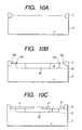
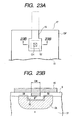
- Fig. 8A shows a top view of a photolectric converting element according to a not claimed third embodiment and Fig. 8B shows a cross-sectional view taken in the line 8B-8B of Fig. 8A .
- the present embodiment is different from the embodiment shown in Figs. 5A and 5B in a point that the photoelectric converting element according to the third embodiment includes a second semiconductor region composed of two regions having different impurity concentrations from each other.
- the inner region 22 in contact with an electrode region 14 has an impurity concentration higher than that of the outer region 12 and lower than that of the electrode region 14.
- the junction depth of the inner region 22 may be smaller or larger than that of the outer region 12.
- Fig. 9 shows a potential profile in the direction along the line 8B-8B of Fig.
- An element isolation region 5 composed of silicon oxide is formed in accordance with a selective oxidizing method in which a silicon nitride film not shown in the drawings is formed as an oxidation-resistant mask and a thick oxide film is formed in a portion exposed therefrom (see Fig. 10A ).
- a photoresist mask not shown in the drawings is formed, ion-implantation is applied thereto and a thermal treatment is carried out to form a p-type second semiconductor region 12 in a first semiconductor region 11 composed of an n-type semiconductor substrate.
- the edge 103 of the second semiconductor region 12 is made apart from the edge 104 of the element isolation region 5 where many defects are found, so that a depletion layer formed by a pn junction is prevented from reaching the edge 104. In such a manner, the generation of a dark current due to the defects can be suppressed.
- the photoresist mask (not shown in the drawings) is formed and the inner region 22 with a high impurity concentration is formed by the ion-implantation and the thermal treatment ( Fig. 10B ).
- An n-type third semiconductor region 13 is formed in accordance with the ion-implantation and the thermal treatment (see Fig. 10C ).
- the p-type electrode region 14 is formed by the ion-implantation and the thermal treatment to obtain a structure shown in Fig. 8B .
- an insulating film is formed to cover surface of a substrate, and openings are formed on the insulating film, and a read and reset circuit formed in another position of the same semiconductor substrate may be connected to the electrode region 14 through a wiring.
- the same circuit as shown in Fig. 7 can be employed as described above.
- Fig. 11A shows the upper surface of a light-receiving element according to a not claimed embodiment.
- Fig. 11B shows a cross-sectional view taken in the line 11B-11B of Fig. 11A .
- the fourth embodiment is different from the second embodiment shown in Figs. 5A and 5B with respect of a point that an n-type epitaxial layer 21 formed on the surface of a p-type semiconductor substrate by epitaxial growth is employed as a first semiconductor region in the fourth embodiment.
- an n-type well formed by ion-implantation and thermal treatment in the p-type semiconductor substrate can be used in place of forming the epitaxial layer 21.
- electric charges generated in the deep position of the p-type semiconductor substrate can be prevented from arriving at a p-type second semiconductor region 12. More specifically, when the thickness of the well is, for example, about 4 ⁇ m, most of holes generated in the position of depth apart by about 4 ⁇ m from the surface of the light-receiving element will flow to the p-type semiconductor substrate. Therefore, the generation of a dark current can be suppressed.
- the second semiconductor region is formed in the well provided for each pixel or provided common to all pixels, hence the entry of the noise can be suppressed.
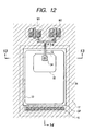
- Fig. 12 shows a top view of a photoelectric converting element according to a not claimed fifth embodiment.
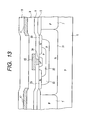
- Fig. 13 shows a cross-sectional view taken in the line 13-13 of Fig. 12 .
- Fig. 14 shows a cross-sectional view taken in the line 14-14 of Fig. 12 .
- a p-type second semiconductor region 32 for forming a photodiode serving as a photoelectric converting element is formed in an opening portion OP. Further, in this region 32, a p-type inner region 22 is formed. In the inner region 22, a p + -type electrode region 34 is formed. The electrode region 34 is electrically connected to the drain part of an MOS transistor M1 as a resetting switch and to the gate part of a source follower MOS transistor M2 as an amplifier element through a wiring 15 made of a first metal layer. Further, the opening portion OP of the photoelectric converting element is defined by a light-shielding layer 17 formed with a second metal layer. The light-shielding layer 17 is connected to a power source and fixed to a predetermined reference potential.
- the p + -type electrode region 34 is arranged nearer a portion where the drain part of the resetting MOS transistor M1 and the source follower MOS transistor M2 are arranged than the center of the opening portion.
- a power source line 16 for determining the potential of an n-type well region 31 serving as a first semiconductor region.
- the size of the opening portion OP is set to 40 ⁇ m ⁇ 60 un.
- the second semiconductor region 32 is formed in the opening portion OP of the n-type well region 31 provided in a p-type semiconductor substrate 6, further, the inner region 22 is formed in the second semiconductor region 32, and the electrode region 34 is provided in the form of an island in the inner region 22.
- an n-type surface region 33 serving as a third semiconductor region is provided and is electrically connected to the n-type well region 31 at the end of the opening portion OP.
- the photodiode is formed by the pn junctions of the second semiconductor region 32 composed of the p-type semiconductor, the inner region 22 and the first and third semiconductor regions 31 and 33 composed of the N-type semiconductors. Photocarriers photoelectrically converted by the photodiode are collected to the electrode region 34 composed of the p + -type semiconductor to change the potential of the wiring 15 formed with the first metal layer.
- a protective film 18 is provided on the light-shielding layer 17 made of the second metal layer.
- the p + -type region 34 is arranged nearer the side where the resetting MOS transistor M1 and the source follower MOS transistor M2 are arranged than the center of the opening portion, that is, in the right side of Fig. 14 .
- the contact of the power source line 16 for supplying a voltage to the n-type well region 31 is arranged only in a side opposite to the p + -type region 34.
- n-type well region 31 is formed in the p-type substrate 6 and the periphery of each pixel is surrounded by a p-type well region 7 serving as an element isolation region and each pixel is electrically separated from another pixel by a pn junction.
- the p-type substrate 6 about 1 ⁇ 10 15 (cm -1 ); the first semiconductor region 31: about 1 ⁇ 10 17 (cm -3 ) and about 4.0 ⁇ m; the second semiconductor region 32: about 2 ⁇ 10 17 (cm -3 ) and about 0.35 ⁇ m; the inner region 22: about 3 ⁇ 10 17 (cm -3 ) and about 0.30 ⁇ m; the third semiconductor region 33: about 3 ⁇ 10 18 (cm -3 ) and about 0.20 ⁇ m; and the electrode region 34: about 3 ⁇ 10 19 (cm -3 ).
- the second semiconductor region 32 about -1.0 V; and the inner region 22: about - 1.5 V.
- the depleting voltage of the second semiconductor region 32 and the inner region 22 becomes higher toward the electrode region 34, the potential slope of the photocarriers is formed, so that the photocarriers can be more efficiently collected to the electrode region 34 part.
- the photo-mask (reticle) for exposure is formed so that each corner portion of the second semiconductor region 32 and the inner region 22 has an obtuse angle, so that the groove of the potential due to the unevenness of electric field in the corner portions is hardly formed.
- a residual image characteristic is improved.
- the region 31 is formed in the p-type semiconductor substrate 6 and has a structure that the periphery for each pixel is surrounded by the p-type well region 7, a crosstalk generated due to the entry of the photocarriers to adjacent pixels can be substantially completely controlled. Thus, a high quality resolution pattern can be obtained.
- the overflowing photocarriers are absorbed by the surrounding p-type well region 7 or the substrate 6. Therefore, a high quality image with less bleeding can be formed without giving any influence to other pixels.
- the second semiconductor region 32 and the inner region 22 are shown in the drawings as the regions for forming the photodiode, for instance, a second p-type inner region which includes the electrode region 34 inside the inner region 22 may be provided, and the impurity concentration and the junction depth of this second inner region may be set so as to have the depleting voltage of the second inner region higher than that of the inner region 22, so that a light-receiving element having a lower residual image characteristic can be formed.
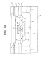
- Fig. 15 shows a top view of a photoelectric converting element according to a sixth embodiment which is in accordance with the present invention.
- Fig. 16 shows a cross-sectional view taken in the line 16-16 of Fig. 15 .
- Fig. 17 shows a cross-sectional view taken in the line 17-17 of Fig. 15 .
- the photoelectric converting element according to the sixth embodiment is different from that according to the fifth embodiment shown in Figs. 12 to 14 in a point that the planar shape of the inner region 22 composed of a p-type semiconductor is changed to a shape with a portion having a gradually changed width.
- the portion 22A having a gradually decreased width toward a lower part of the drawings is extended downward beyond the center of a light-receiving surface (opening portion) from the upper part of the drawings.
- Reference numeral 8 denotes a contact region with a high impurity concentration and serves as a cathode contact.
- the second semiconductor region 32 of a photo-diode serving as a photoelectric converting element is formed in an opening portion OP.
- An inner region 22 is formed in the second semiconductor region 32.
- An electrode region 34 is formed in the inner region 22.
- the electrode region 34 is electrically connected to the drain part of a resetting MOS transistor M1 and the gate part of a source follower MOS transistor M3 through a wiring 15 made of a first metal layer.
- the opening portion OP of the photoelectric converting element is defined by a light-shielding layer 17 formed with a second metal layer, and the light-shielding layer 17 is connected to a power source and fixed to a desired potential.
- the electrode region 34 is arranged nearer a portion where the drain part of the resetting MOS transistor M1 and the source follower MOS transistor M2 are arranged than the center of the opening portion, and a power source line 16 for supplying a reverse bias voltage to an n-type well region 31 as a first semiconductor region is provided in the opening portion side opposite to the electrode region 34.
- the size of the opening portion OP is set to 40 ⁇ m ⁇ 60 ⁇ m.
- an n-type surface region 33 serving as a third semiconductor region is provided on the major surfaces of the second semiconductor region 32 and the inner region 22 and is electrically connected to the n-type well region 31.
- the photodiode is formed by the pn junction between the p-type second semiconductor region 32 and the inner region 22 and the n-type well region 31 and the n-type surface region 33, hence photocarriers photoelectrically converted by the photodiode are collected to the electrode region 34 to change the potential of the wiring 15.
- a protective film 18 is provided on the upper part of the light-shielding layer 17 formed with a second metal layer.
- the electrode region 34 is arranged nearer the side where the resetting MOS transistor M1 and the source follower MOS transistor M2 are arranged than the center of the opening portion, that is to say, in the right side of Fig. 17 .
- the contact of the power source line 16 for supplying the potential to the n-type well region 31 is arranged only in a side opposite to the electrode region 34 (the left side of Fig. 17 ).
- the n-type well region 31 is formed in a p-type semiconductor substrate 6 and has a structure in which the periphery of the region 31 is surrounded by a p-type well region 7 for each pixel and the region 31 is electrically isolated for each pixel.
- the inner region 22 has a shape that its width gradually increases from W1 to W2 (W2 > W1) toward the electrode region 34. Still further, the corner parts of the upper surfaces of the second semiconductor region 32 and the inner region 22 are formed in such a manner that they are all composed of obtuse angles larger than 90°.
- the p-type substrate 6 about 1 ⁇ 10 15 (cm -3 ); the first semiconductor region 31: about 1 ⁇ 10 17 (cm -3 ) and about 4.0 ⁇ m; the second semiconductor region 32: about 2 ⁇ 10 17 (cm -3 ) and about 0.35 ⁇ m; the inner region 22: about 3 ⁇ 10 17 (cm -3 ) and about 0.30 ⁇ m; the third semiconductor region 33: about 3 ⁇ 10 18 (cm -3 ) and about 0.20 ⁇ m; and the electrode region 34: about 3 ⁇ 10 19 (cm -3 ).
- the depleting voltages of the second semiconductor region 32 and the inner region 22 in the sixth embodiment is shown below.
- the second semiconductor region 32 about -1.0 V; and the inner region 22: about -1.5 V.
- the depleting voltages of the second semiconductor region 32 and the inner region 22 become higher toward the electrode region 34, the potential slope of the photocarriers is formed, so that the photocarriers can be more efficiently collected to the region 54.
- the power source line 16 for supplying a voltage to fix the potential of the n-type well region 31 serving as the first semiconductor region is provided in a side opposite to the electrode region 34, a photocurrent due to photo-generated electrons flows through the n-type well region 31 toward the contact region 8.
- a potential slope is formed from the contact region 8 toward the electrode region 34, so that photo-generated holes can be more efficiently collected to the electrode region 34 to improve a residual image characteristic.
- the inner region 22 has a portion having a width increased toward the electrode region 34, when the photo-generated holes reaching the tip end of the inner region 22 flow toward the electrode region 34 due to the potential slope, the sheet resistance of the inner region 22 is gradually decreased relative to the photocurrent due to the photo-generated holes, whereby the photo-generated holes can be collected to the electrode region 34 at high speed. As the result, the residual image characteristic during a high speed operation can be improved. Further, since the tip end of the inner region 22 is arranged beyond the center of the opening portion OP, the collecting efficiency of the holes in the side of the contact region 8 is improved.
- each corner portion of the second semiconductor region 32 and the inner region 22 is formed so as to have an obtuse angle, so that the groove of the potential due to the unevenness of electric field in the corner portions is hardly formed, thereby the residual image characteristic is more improved.
- Such shape can be easily formed by the pattern of a photomask employed during the exposure of a photoresist.
- n-type well region 31 is formed in the p-type semiconductor substrate 6 and has a structure that the periphery is surrounded by the p-type well region 7 for each pixel, a crosstalk generated due to the entry of the photocarriers to adjacent pixels can be substantially completely controlled, whereby a high quality resolution pattern can be obtained.
- the second semiconductor region 32 and the inner region 22 are shown in the drawings as the regions for forming the photodiode, for instance, a second inner region which further includes the electrode region 34 inside the inner region 22 may be provided and the impurity concentration and the junction depth of the second inner region may be set so as to have the depleting voltage of the second inner region higher than that of the inner region 22, so that a photoelectric converting element having a low residual image characteristic can be formed.
- Fig. 18 shows a top view of a light-receiving.. element according to a seventh embodiment not claimed.
- Fig. 19 shows a cross-sectional view taken in the line 19-19 of Fig. 18 .
- the feature of a light-receiving element according to the seventh embodiment resides in a point that a doped region 43 with a low impurity concentration is formed in an offset region provided between an electrode region 34 and a semiconductor region 33.
- a p-type region serving as the second semiconductor region 32 of a photodiode as a light-receiving element is formed in an opening portion OP.
- a p + -type region as an electrode region 34 formed in the p-type region 32 of the photodiode is electrically connected to the drain part of a resetting MOS transistor M1 and the gate part of a source follower MOS transistor M2 through a wiring 15 made of a first metal layer.
- the opening portion OP of the light-receiving element is defined by a light-shielding layer 17 made of a second metal layer.
- the light-shielding layer 17 is connected to a power source and fixed to a desired potential.
- the size of the opening portion OP is set to 40 ⁇ m ⁇ 40 ⁇ m.
- the p-type semiconductor region 32 is formed in the opening portion OP of an n-type well region 31 provided in a p-type semiconductor substrate 6, and the p + -type electrode region 34 is provided in the p-type second semiconductor region 32 in the form of an island.
- an n-type surface region 33 serving as a third semiconductor region is provided and is electrically connected to the n-type well region 31.
- the n-type surface region 33 is arranged with an offset (space) of about 2 ⁇ m not so as to bring it into contact with the p + -type electrode region 3.4. Further, a second n-type surface region 43 is formed on the entire surface of the light-receiving element including this offset region.
- the photodiode is formed by the pn junction of the p-type semiconductor region 32 and the n-type regions 31, 33 and 43. Photocarriers photoelectrically converted by the photodiode are collected to the p + -type electrode region 34 to change the potential of the wiring 15 made of the first metal layer.
- interlayered insulating films 9 are provided between the surface of the semiconductor and the first metal layer and between the first metal layer and the second metal layer, and a protective film 18 is provided on the upper part of the light-shielding layer 17 formed with the second metal layer.
- the p-type substrate 6 about 1 ⁇ 10 15 (cm -3 ); the n-type well region 31: about 1 ⁇ 10 17 (cm -3 ) and about 4.0 ⁇ m; the p-type second region 32: about 2 ⁇ 10 17 (cm -3 ) and about 0.35 ⁇ m; the first n-type surface region 33: about 3 ⁇ 10 18 (cm -3 ) and about 0.20 ⁇ m; the second n-type surface region 43: about 3 ⁇ 10 17 (cm -3 ) and about 0.1 ⁇ m; and the p + -type region 34 : about 3 ⁇ 10 19 (cm -3 ).
- the vicinity of the surface of the offset region becomes a p-type region with an impurity concentration of 10 17 (cm -3 ) or less. Further, since the concentration of boron in the vicinity of the surface of the semiconductor tends to be varied depending on a production process, carriers generated in the offset region result in generation of a dark current and unevenness in the dark current.
- the surface concentration of the second n-type surface region 43 is set to 10 17 to 10 18 (cm -3 ) or so, so that even when reverse bias is applied between the p + -type region 34 and the first n-type surface region 33, a trouble such as a breakdown will not be generated.
- the p + -type region 34 is brought into contact with the first n-type surface region 33 with a high probability due to a disalignment in a photolithography, thereby decreasing a yield.
- the surface vicinity of the offset region becomes an n-type region with the concentration of about 10 17 (cm -3 ) because of the n-type semiconductor serving as a low concentration-doped region 43, the generation of the carriers in the offset region can be suppressed.
- this surface region gives substantially seldom any effect to the first n-type surface region 33 and the p + -type region 34, because the impurity concentration of the second n-type surface region 43 is sufficiently lower than those of the regions 33 and 34. Since there is no problem of disalignment in the photolithography as described above, the surface concentration of the offset region can be selectively controlled and a dark current can be reduced.
- the dark current obtained when there exists the second n-type surface region 43 is reduced by 1/3 times lower than that obtained when the surface region 43 is not provided.
- the depleting voltage of the semiconductor region 32 according to the seventh embodiment of the present invention is about -2V. Therefore, for example, when the n-type well region 31 is connected a source voltage during an operation under the source voltage of 5V, when the potentials of the p + -type region 34 and the wiring 15 are 3V or lower, the p-type region 32 is depleted and thereby a neutral region disappears.
- the above-described depleting voltage sensitively changes mainly relative to the impurity concentration and the junction depth of each of the n-type well region 31, the p-type region 32 and the first n-type surface region 33. Accordingly, the unevenness of the depleting voltage in production is relatively increased, for example, by about ⁇ 1.0V for ⁇ 3 ⁇ . However, when the depleting voltage and an operating point are set in a suitable range, a high yield can be maintained even in the case of unevenness in the depletion voltage.
- the n-type surface region 43 is provided in order to suppress the generation of the carriers on the surface of the offset region, it is possible to provide the second surface region, which is not limited to n-type, and a p-type second surface region may be provided so that the suppression of the dark current can be also realized. In this case, the p-type neutral region is increased. When there remains an allowance in the capacitance of the light-receiving portion in view of design, the surface region may be made p-type.
- the impurity concentration in the offset region may be set in a range of about 10 16 to 10 18 cm -3 , more preferably, in a range of 5 ⁇ 10 16 to 5 ⁇ 10 17 cm -3 from the viewpoints of the decrease of the dark current and the prevention of the breakdown.
- the n-type well region 31 is formed in the p-type substrate 6 and has a structure in which the periphery of the n-type well region 31 is surrounded by a p-type well region 7 for each pixel.
- n-type well region 31 and a p-type region 7 are formed on the surface side of a p-type semiconductor substrate 6.
- a field insulating film 5 is formed by selective oxidation.
- an n-type semiconductor region 33 is formed on the surface thereof.
- Ion-implantation is applied to the surface of the semiconductor substrate to form an n-type semiconductor layer 43. Then, a p-type electrode region 34 is formed.
- a space between the electrode region 34 and the semiconductor region 33 is preferably set in a range of 0.4 ⁇ m to 1.5 ⁇ m, and more preferably in a range of 0.5 pm to 1.0 pm.
- the impurity concentration of the offset region is set to a concentration lower, by one figure or more, than that of the semiconductor region 33 or the electrode region 34, and further higher than that of the semiconductor region 32.
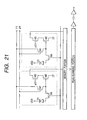
- Fig. 21 shows a circuit diagram of the read and reset circuit.
- D1 denotes a photodiode functioning as a photoelectric converting element according to each of the respective embodiments.
- M2 and a constant-current source which is not shown in Fig. 21 constitute a source follower as a pair.
- M1 denotes a resetting switch.
- M3 indicates a selecting switch.
- M4 denotes a transfer switch for transferring signals of the photodiode as photocharges to the input terminal of the source follower.
- the photosignals and reset signals read from the source follower are respectively transferred to a memory portion and outputted to an external part through a scanning circuit or the like.
- the area of the electrode is specially restricted to 1 ⁇ m square, so that the junction capacitance can be restricted to 0.1 fF.
- a solid image pick-up apparatus can be provided with a high yield, in which reset noise can be suppressed to four electrons or so and a residual image is not formed even within a dynamic range of 10 bits.
- Fig. 22 is an equivalent circuit of one pixel of the read and reset circuit.
- each pixel comprises a photoelectric converting element D1, a resetting MOS switch M1 for resetting the photoelectric converting element D1, a first MOS source follower M2 for converting a signal charge of the photoeletric converting element D1 to a voltage signal, a MOS switch M3 for holding a noise signal during the storage period of the noise signal upon reset of the photoeletric converting element D1, a retention capacitance 605, a second MOS source follower M4 for conducting impedance conversion of the signal of the retention capacitance 605, a MOS switch 607 for reading a noise signal charge immediately after a reset operation, a noise signal retention capacitance 609, a MOS switch 608 for reading photosignal charges after the photosignals are stored and a photosignal retention capacitance 610.
- the read and reset circuit includes a shift register 613 for successively reading out the noise signal of the noise signal retention capacitance 609 and the photosignal of the photosignal retention capacitance 610 to a common noise signal output line 690 and a common optical signal output line 691, respectively; buffer amplifiers 614 and 614' for conducting impedance conversion of voltages of the common noise signal output line 690 and the common photosignal output line 691; a differential amplifier 615 for obtaining the differential signal of the voltage of the common noise signal output line 690 and the common photosignal output line 691 and amplifying the differential signal and an output buffer amplifier 692 for conducting impedance conversion of the output of the differential amplifier 615 and outputting the signal thus obtained to the external part of a photoelectric conversion device.
- the read and reset circuit includes a common output line reset means 693 for resetting the common noise signal output line 690 and the common photosignal output line 691 for each reading operation of one pixel.
- V1PD and V2PD are set to a depletion region in the photoelectric converting element portion, so that the photoelectric conversion device with a high sensitivity can be realized.
- the total of the junction capacitance of the electrode region of the light-receiving element, the capacitance of the gate of the source follower MOS, the junction capacitance of the drain part of the reset MOS and a parasitic capacitance such as a wiring capacitance or the like is about 25 fF.
- the depleting region of the light-receiving element portion is in a range of 1V to 5V.
- the operating point in the present embodiment is a point smaller than 1V which is a minimum value of the depleting region, even when the depleting voltage has the unevenness of about ⁇ 2V, a high yield can be maintained.
- the potential of the photoelectric converting element portion just after the resetting operation is smaller than the reset voltage (Vres), because an NMOS is employed for the reset switch and the potential of the photoelectric converting element portion is shifted to a minus side when the reset switch is turned off.
- the present invention may be applied to other photoelectric conversion devices or solid image pick-up devices.
- 344 pieces of pixels each having the above-described structure are provided to form a primary photoelectric conversion device, which is not shown in the drawings.
- the photoelectric conversion device is employed to constitute a contact type image sensor, and it is used as the image reading device of an image input system such as a facsimile machine or an image scanner.
- an image input system such as a facsimile machine or an image scanner.
- Fig. 23A shows a top view of a light-receiving element portion according to the eighth embodiment.
- Fig. 23B shows a cross-sectional view taken in the line 23B-23B of Fig. 23A .
- reference numeral 51 denotes a first semiconductor region
- 52 indicates a second semiconductor region.
- the conductivity types of these regions are n-type and p-type, respectively.
- the second semiconductor region 52 is formed in an opening portion OP defined by a light-shielding layer 17.
- a depletion layer DL is formed by the pn junction of the first semiconductor region 51 and the second semiconductor region 52. Reverse bias is applied between the first semiconductor region 51 and the second semiconductor region 52, and the larger portion of the depletion layer DL is extended to the side of the first semiconductor region 51 having a low impurity concentration.
- An electrode 15 is connected to the second semiconductor region 52 through the contact hole CH of an insulating film 9.
- the quantity of the crystal defects is increased due to a damage in an etching process and the quantity of the dark current is increased.
- a portion 59 where the depletion layer DL is brought into contact with the insulating film 9 is covered with the electrode 15 through the insulating film 9. Therefore, the etching damage in formation of the electrode gives no influence on the depletion layer DL, so that dark current can be reduced.
- the electrode 15 is designed to be always formed in the portion 59 where the depletion layer DL is brought into contact with the insulating film 9 by taking disalignment generated in photolithography into consideration. Accordingly, the quantity of the crystal defects generated in the vicinity of the depletion layer DL can be prevented from being varied depending on process unevenness. Therefore, the unevenness of the dark current due to the process unevenness can be lowered.
- metals, alloys and compounds such as Al, Al alloys, Ti, Ti alloys, W, W alloys, Co, Co alloys, Ta, Ta alloys, Mo, Mo alloys, Cu, Cu alloys, WN, TiN, TaN, Cr, Cr alloys, etc. may be employed. Otherwise, a plurality of kinds of materials may be laminated.
- electrically conductive materials for example, a material containing silicon as a main component such as doped polysilicon.
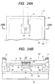
- Fig. 24A shows a:top view of a light-receiving element and Fig. 24B shows a cross-sectional view taken in the line 24B-24B of Fig. 24A .
- Reference numeral 66 denotes an n-type semiconductor substrate
- 67 indicates an embedded n + -type region formed by implanting ions into the n-type semiconductor substrate 66.
- 61 denotes an n-type epitaxial layer as a first semiconductor region formed on the n + -type region 67.
- 68 denotes an n + -type region in contact with the embedded n + -type region, which is formed by implanting ions into the ntype epitaxial layer 61.
- reference numeral 62 denotes a second semiconductor region and an electrode region which is specifically composed of a p-type region with a high concentration of impurities.
- 63 indicates an n-type region which is provided in order to suppress the spread of the a depletion layer DL on the major surface of the substrate, that is to say, the surface of the epitaxial layer.
- the electrode 15 formed with a metal or the like including Al as a main material is electrically connected to the electrode region 62 through the contact hole CH of an insulating film 9.
- 17 indicates a light-shielding layer.
- OP indicates an opening portion.
- 5 denotes an insulating film for isolating the element.
- 9 denotes an interlayered insulating film for insulating the light-shielding layer 17 and an electrode 28.
- the semiconductor portion composed of the n-type semiconductor substrate 66, the n + -type region 67, the n - -type epitaxial layer 61, the n + -type region 68, the n-type region 63 and the electrode region 62 is referred to as "substrate”.
- the n - -type epitaxial layer 61 has a structure that it is surrounded by the n + -type regions 67 and 68 located under the lower portion and in the periphery thereof. Thus, a potential barrier is formed. As a result, positive holes of carriers generated by light are finally collected to the p-type electrode region 62 having the lowest potential.
- the depletion layer DL is formed around the electrode region 62.
- the impurity concentration of the electrode region 62 is set to about 3 ⁇ 10 19 cm -3 and the impurity concentration of the n-type region 63 is set to about 2 ⁇ 10 17 cm -3 .
- the width of layer of the depletion layer DL becomes approximately 0.14 ⁇ m.
- Most of the depletion layer DL is expanded to the side of the n - -type region 61 from the pn junction surface of the electrode region 62 and the n - -type region 61.
- the extension of the depletion layer DL is suppressed by the n-type region 63.
- the electrode 15 is arranged so as to be larger, for instance, by 0.4 ⁇ m than the electrode region 62 so that the upper side of a portion where the depletion layer DL comes into contact with the insulating film 9 is covered with the electrode. Therefore, crystal defects generated owing to an etching damage or a damage due to ashing of a resist upon formation of the electrode 15 give no adverse effect to the depletion layer DL, so that a dark current can be reduced.
- the dark current generated when the electrode 15 is formed so as to cover the portion 59 where the depletion layer DL comes into contact with the insulating film 9 is covered with the electrode and the dark current generated when the electrode is not formed so the dark current generated when the upper part of the portion where the depletion layer DL comes into contact with the insulating film 9 is completely covered with the electrode 15 can be reduced to 2/3 as low as that of the latter. In other words, the dark current can be reduced depending on the size and the formed position of the electrode 15.
- the semiconductor substrate 66 and the regions 67 and 68, the epitaxial layer 61 and the region 63 are determined to be the n-types, and the region 62 is determined to be the p-type, needless to say, the present embodiment is not limited to the above-described conductivity types, and each of the above-described conductivity types may be changed to an opposite conductivity type.
- the n - -type epitaxial layer 61 has a structure that it is surrounded by the n + -type regions 67 and 68 to form the potential barrier.
- the photocarriers do not enter adjacent pixels, so that the generation of a crosstalk can be substantially completely controlled and a high quality resolution pattern can be thus obtained.
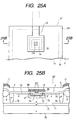
- Fig. 25A shows a top view of a light-receiving element and Fig. 25B shows a cross-sectional view taken in the line 25B-25B of Fig. 25A .
- reference numeral 76 denotes an n-type semiconductor substrate.
- 77 denotes an embedded n + -type region formed by implanting ions into the n-type semiconductor region 76.
- 71 is an n - -type epitaxial layer as a first semiconductor region formed on the n + -type region 77.
- 78 denotes an n + -type region formed by implanting ions into the n - -type epitaxial layer and surrounding the periphery of the epitaxial layer 71.
- 72 indicates a second semiconductor region.
- 74 denotes an electrode region which is specifically composed of a p-type region with a high concentration of impurities.
- 73 denotes an n-type region provided for suppressing the extension of a depletion layer DL on the major surface of the substrate.
- 15 indicates an electrode and is formed with a metal or the like including Al as a main material. The electrode 15 is electrically connected to the electrode region 74 through the contact hole CH of an insulating film 9.
- a p-type semiconductor region 72 is provided in order to suppress this phenomenon.
- OP denotes an opening portion.
- 5 denotes an insulating film for isolating the element.
- An upper interlayered insulating film 9 functions as an insulating film for insulating a light-shielding layer 17 and an electrode 15.
- the portion composed of the n-type semiconductor substrate 76, the n + -type region 77, the n - -type epitaxial layer 71, the n + -type region 78, the n-type region 73 and the electrode region 74 is referred to as "substrate”.
- the n - -type epitaxial layer 71 has a structure that it is surrounded by the n + -type regions 77 and 78. Thus, a potential barrier is formed. As a result, positive holes of carriers generated by light are finally collected to the p-type electrode region 74 having the lowest potential.
- the depletion layer DL is formed around the p-type region 72.
- the impurity concentration of the p-type region 72 is set to about 3 ⁇ 10 18 cm -3 and the impurity concentration of the n-type region 73 is set to about 2 ⁇ 10 17 cm -3 , and when the reverse bias voltage of 3V is applied thereto, the width of layer of the depletion layer DL becomes approximately 0.15 ⁇ m.
- Most of the depletion layer DL is expanded to the side of the n-type region 71 from the pn junction surface of the p-type region 72 and the n-type region 71.
- the electrode 15 is arranged so as to be larger, for instance, by 0.4 ⁇ m than the p-type region 72 so that a portion 69 where the depletion layer DL comes into contact with the insulating film 9 is covered with the electrode. Therefore, crystal defects generated on the surface of the substrate owing to an etching damage or a damage due to ashing of a resist upon formation of the electrode 15 give no adverse effect to the depletion layer DL, so that a dark current can be reduced.
- the substrate 76 and the regions 77 and 78, the epitaxial layer 71 and the region 73 are determined to be the n-types, and the regions 72 and 74 are determined to be p-types, needless to say, the present embodiment is not limited to these conductivity types, and each of these conductivity types may be changed to an opposite conductivity type.
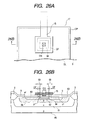
- Fig. 26A shows a top view of a light-receiving element according to the eleventh embodiment not claimed and Fig. 26B shows a cross-sectional view taken in the line 26B-26B of Fig. 26A .
- reference numeral 86 denotes a p-type semiconductor substrate.
- 81 denotes an n-type region serving as a first semiconductor region.
- 82 denotes a p-type region serving as a second semiconductor region.
- 83 denotes an n + -type region serving as a third semiconductor region.
- 84 is a p-type region which is an electrode region with a high concentration of impurities, that is to say, is composed of a p + -type region.
- the p + -type region 84 is arranged on the major surface of the substrate via the n + -type region 83 and an offset region OF disposed therebetween.
- 15 denotes an electrode formed with a metal or the like including Al as a main component.
- the electrode 15 is electrically connected to the p + -type region 84 through the contact hole CH of an insulating film 9 formed on the major surface of the p-type substrate 86.
- DL denotes a depletion layer.
- the p-type region 82 is interposed between the n-type region 81 and the n + -type region 83.
- the depletion layers DL are formed by a pn junction in the lower surface side and by a pn junction in the upper surface side of the p-type region 82, and a state of a groove with a low potential in the semiconductor region 82.
- the positive holes of electric charges generated by light are collected to the p-type region 82, and finally collected to the p + -type region 84 having the lowest potential.
- the impurity concentration of the n-type region 81, the impurity concentration and the junction depth of the p-type region 82 and the n + -type region 83 as well as the bias voltage of the pn junctions thereof are properly set, whereby the substantially entire part of the n-type region 81 can be also depleted.
- the p-type region 82 hardly contributes to the capacitance of the light-receiving element, hence the capacitance of the light-receiving element can be reduced.
- the offset regions OF of 1 ⁇ m are provided between the p + -type region 84 and the n + -type region 83 at the right side and between the p + -type region 84 and the n + -type regions 83 at the left side, respectively.
- the electrode 15 is formed so as to cover a portion 89 in which the depletion layer DL comes into contact with the insulating film 9 with the electrode. Therefore, crystal defects formed on the surface of the substrate due to an etching damage or a damage owing to the ashing process of a resist upon formation of the electrode 15 do not apply any influence to the deplation layer DL, so that the dark current can be reduced.
- the present embodiment is not limited to the above-described conductivity types, and each of the conductivity types employed in the present embodiment may be changed to an opposite conductivity type.
- the n-type region 81 is formed in the p-type substrate 86, the photocarriers can be prevented from entering adjacent pixels. Therefore, the generation of a crosstalk can be substantially completely controlled, so that a high quality resolution pattern can be realized.
- the p-type semiconductor substrate 86 is prepared and the n-type region 81 composed of the n-type semiconductor is formed (see Fig. 27A ).
- a field insulating film 5 is formed in accordance with a selective oxidation method, and then, the p-type semiconductor region 82 is formed (see Fig. 27B ).
- the p-type electrode region 84 is formed.
- the offset region between the n-type semiconductor region 83 and the electrode region 84 may be implanted by dopant ions with a low impurity concentration (see Fig. 27C ).
- the insulating film 9 composed of PSG, BSG, BPSG or the like is formed, and the opening CH is formed on the electrode region 84 (see Fig. 28A ).
- a layer 15 made of a conductive material such as Al-Cu, etc. is formed by sputtering or the like (see Fig. 28B ).
- a barrier metal composed of TiN or the like may be formed below the layer 15.
- the layer 15 made of the conductive material is subjected to a patterning process by dry-etching using BCl 3 , Cl 2 , etc., whereby the layer 15 is left so that the offset portion is covered with the layer 15. In such a manner, an anode electrode 15 can be obtained.
- Each of the light-receiving elements described in the above embodiments 8 to 11 can applied to the read and reset circuits shown in Figs. 4 , 7 , 21 and 22 , respectively.
- the present invention may be preferably applied to the photoelectric conversion device proposed in Japanese Patent Application Laid-Open No. 9-205588 and can be also applied to, for instance, other photoelectric conversion devices or solid image pick-up devices.
- the photoelectric conversion device to which the present embodiments can be applied is employed to produce a contact type image sensor, which is used as the image reading device of an image input system such as a facsimile machine or an image scanner.
- a contact type image sensor which is used as the image reading device of an image input system such as a facsimile machine or an image scanner.
- the photoelectric converting element capable of reducing the dark current can be obtained, and the photoelectric conversion device with high performance can be achieved with less unevenness of the dark current even when production process is varied. Therefore, it is possible to provide an inexpensive image reading device or an image input system capable of obtaining a high quality image.
Description
- The present invention relates to a photoelectric converting element of an image sensor used for such an image-reading system as a digital camera, an image scanner, a facsimile, a copying machine, etc., as well as a photoelectric conversion device comprising the photoelectric converting element, specifically to the structure of a photoelectric converting element suitable for a photoelectric conversion device such as a close contact type image sensor, which is provided with a comparatively large photoelectric converting element having the opening portion of a pixel with several tens microns or more in size.
- Document
US 4,652,899 discloses a radiation-sensitive semiconductor device having a reduced capacitance. Specifically, the capacitance of a radiation-sensitive diode can be considerably reduced by giving it the form of a pn junction (4) between a first semiconductor region (4) and a layer-shaped semiconductor zone, which in operation is fully depleted. The speed of such a diode is favorably influenced by the choice or the shape of the geometry of the layer-shaped zone. When the latter is formed with parts decreasing in width of thickness, an electric field is produced in these parts which accelerates the transport of minority charge carriers to a central contact. - Furthermore,
document EP 0 854 516 A2 , with respect to which the two-part from has been drafted discloses a partially pinned photodiode for solid state image sensors. Specifically, a pixelated image sensor comprising a partially pinned photodiode which is formed a semiconductor of a first conductivity type formed on a surface of the sensor with at least one photodiode formed within the semiconductor near the surface is disclosed. Further, the photodiode being formed from a second conductivity type opposite the first conductivity type; a pinning layer formed on the surface over at least a portion of the photodiode creating a pinned photodiode region, the pinning layer being formed from the first conductivity type; an unpinned region formed near the surface in an area outside the portion used to form the pinning layer, and the unpinned region is formed as a floating region that is employed as a capacitor. The partially pinned photodiode is useful in expanding the fill factor of photodetectors employing photodiode technology. - Moreover, document
US 5,514,887 discloses a solid state image sensor having a high photoelectric conversion efficiency. Specifically, in a solid state image sensor comprising a first impurity layer of a first conductivity type forming a photodiode, the impurity layer is composed of a first impurity region formed of a low concentration at a deep level, and a second impurity region formed of a high concentration at a shallow level. The first impurity region extends under a second impurity layer of a second conductivity type formed for device isolation, and also extends under a gate region of a transistor for transferring an electric charge from the photodiode to a CCD channel. - In recent years, CCD image sensors, non-CCD image sensors such as CMOS image sensors, etc. have been positively developed as photoelectric conversion devices.
- Generally, a photodiode comprising a PN junction of a semiconductor is used for light-receiving elements of these photoelectric conversion devices.
- For example, as disclosed by Japanese Patent Application Laid-Open No.
55-154784 -
Figs. 29A and 29B show a structure of a conventional light-receiving element.Numeral 201 indicates an n-type semiconductor substrate; 202: a p-type semiconductor layer; 203: an n-type semiconductor layer having an impurity concentration of 5 × 1015 cm-3 to 10 × 1015 cm-3 and a thickness of 0.2 µm to 0.3 µm; 205: a thermal oxide film; 208: an n+ channel stopper; 209: an anti-reflection coating film consisting of nitride; 215 and 216: aluminum electrodes; 228: an n+-type semiconductor layer; and 238: a surface electrode. Symbol DL indicates a depletion layer; and DLS: a surface side portion of the depletion layer. - The anode of a photodiode is formed only with a p-
type semiconductor layer 202. When the impurity concentration is lowered, therefore, the property of the ohmic contact with theelectrode 215 is degraded. On the contrary, when the impurity concentration is increased, the depletion layer DL is not extended into thesemiconductor layer 202. - As disclosed by Japanese Patent Application Laid-Open No.
61-264758 -
Fig. 30 shows a top view of a conventional photoelectric conversion device such as a CCD image sensor.Numeral 301 indicates a p-type substrate andnumeral 302 indicates an n+-type accumulating portion. - A portion surrounded by the n+-
type accumulating portion 302 on the p-type substrate 301 is a p-type photoelectric conversion region functioning as a pixel. Symbol PG indicates a photo-gate; SG: a shift-gate; and SR: a CCD shift-register. - In this structure, the PN junction area is reduced, but the PN junction periphery length is increased. It is therefore impossible to sufficiently reduce the capacitance of the PN junction, whereby the sensitivity cannot be increased so much.
- For example, as disclosed by Japanese Patent Application Laid-Open No.
1-303752 -
Fig. 31 shows a cross-sectional view of a light-receiving element of prior art. InFig. 31 ,numeral 301 indicates a P-type semiconductor region; 302: an N-type semiconductor region; 303: a P-type shallow channel stop layer; 305: a field oxide film; 306: a P-type substrate; 308: a P-type channel stop layer; 309: an interlayered insulating film; 317 :a light-shielding film for forming an opening portion (OP). A depletion layer (DL) is extended into the P-type semiconductor region 301, whereby electrons of the generated photocarriers (PC) are collected in the N-type semiconductor region 302 by to an internal magnetic field. - For example, as disclosed by Japanese Patent Application Laid-Open No.
64-14958 -
Fig. 32 shows a cross-sectional view of a light-receiving element of prior art. InFig. 32 ,numeral 406 indicates an N-type substrate; 401: a P-type semiconductor region; 402: an N-type semiconductor region; 403: a shallow P-type semiconductor layer; 408: a P+-type channel stop layer; 409: an insulating film; 415: an electrode consisting of polysilicon; and 420: an N-type region of a CCD register. - On the other hand, a photoelectric conversion device employing a light-receiving element is proposed, for example, in Japanese Patent Application Laid-Open No.
9-205588 - However, when a light-receiving element is employed for an amplifying type photoelectric conversion device which accumulates photo-generated carriers and reads out a signal voltage from a PN photodiode by using charge-voltage conversion means, the sensitivity of the photoelectric conversion device may be degraded in some cases.
- For such an amplifying type photoelectric conversion device, the light output is represented by the following formula (1):

wherein Qp is the quantity of a charge accumulated in the PN photodiode and Cs is a capacitance of the photodiode. - The capacitance Cs of this photodiode can be represented by the formula (2) as shown below, for example, for an amplifying type photoelectric conversion device having a pixel in which an MOS source follower or a reset MOS transistor is connected to a photodiode:

Wherein Cpd is a PN junction capacitance of the PN photodiode itself including a light-receiving portion, Ca is the other capacitance of portions connected to the photodiode, and in the above case the other capacitance includes the gate capacitance of the MOS transistor constituting the MOS source follower, the capacitance of the junction between the source and the well of the reset MOS transistor, the overlapping capacitance of the source and the gate, the wiring capacitance, and the like. - Consequently, to realize high sensitivity, it is indispensable that the photo-generated carriers are effectively accumulated and the capacitance of the photodiode for accumulating the carriers is reduced as much as possible.
- On the other hand, when light is made incident in the photodiode, electric charges generate in the photodiode and electric charges in and around the depletion layer formed due to a PN junction surface in the semiconductor substrate gather at an anode or a cathode. In this case, when an electrode is attached to this anode or cathode, the electric charges can be taken out as electric signals.
-
Fig. 33 is a cross-sectional view of a light-receiving element of prior art provided with an electrode. InFig. 33 ,numeral 701 indicates a first semiconductor region, andnumeral 702 indicates a second semiconductor region to be used as an anode. The conductivity types of those regions are N-type and P-type, respectively. In addition, symbol DL is a depletion layer formed by a PN junction between thefirst semiconductor region 701 and thesecond conductor region 702. Although not illustrated inFig. 33 , a reverse bias is applied to between thefirst semiconductor region 701 and thesecond semiconductor region 702. In addition,numeral 715 indicates an electrode, which is connected to thesecond semiconductor region 702 through a contact hole CH of theinsulating film 709. - The
electrode 715 is composed of a metal, for example, A1 as a main component. Theelectrode 715 is connected to an electrode region formed on the major surface of the semiconductor substrate through a contact hole CH of the insulating film covering the surface of the photodiode. Generally, such light-receiving element is composed by connecting a conductive material such as A1 to a semiconductor region so as to obtain photosignals generated by photocarriers photoelectric-converted in the semiconductor region. - For example, when a general RIE (reactive ion etching) method is employed to form this electrode, then over-etching is usually conducted so as to remove unnecessary portions. In this over-etching, however, some ions accelerated by an electrical field pass through the
insulating film 709 and reach the major surface of the semiconductor substrate and then damage the vicinity of the interface between the semiconductor and the insulating film, thereby resulting in generation of crystal defects in some cases. - Crystal defects may also generate due to the plasma ashing of a photoresist, etc. even in a step after the electrode is formed, just like in the above case.
- In the case of a general light-receiving element, a PN junction exists around a semiconductor region formed on the major surface of the semiconductor substrate to which an electrode is connected and the junction surface reaches the vicinity of the interface between the major surface of the semiconductor substrate and the insulating film in many cases.
- Consequently, when an electrode is formed at an inner portion from the junction surface reaching the major surface of the semiconductor substrate, crystal defects due to etching damage generate in the vicinity of the junction surface, and the crystal defects become centers for causing carriers to be generated. The crystal defects generated at a portion of the depletion layer cause a dark current to be generated.
- The generated dark current as described above also becomes a factor for causing the dark current to be varied, since the quantity of the crystal defects generated in the vicinity of the interface or the quantity of crystal defects themselves is changed by misalignment of a mask in formation of electrodes, etc. and etching conditions.
- The first object of the present invention is to provide a photoelectric converting element wherein photo-generated holes can be collected to the electrode region at high speed.
- According to the present invention this is achieved by the subject-matter of the appended independent claim. Advantageous modifications are set forth in the appended dependent claims.
-
Fig. 1A is a top view of a light-receiving element according to a not claimed 1st embodiment; -
Fig. 1B is a cross-sectional view of the light-receiving element according to the not claimed 1st embodiment; -
Fig. 1C is a schematic diagram showing a potential profile in the horizontal direction of the light-receiving element according to the not claimed 1st embodiment; -
Fig. 1D is a schematic diagram showing a potential profile in the vertical direction of the light-receiving element according to the first claimed 1st embodiment; -
Fig. 2 is a graph showing an impurity concentration distribution in the light-receiving element according to the not claimed 1st embodiment; -
Fig. 3 is a graph showing the relationship between an applied voltage and the capacitance of the light-receiving element according to the not claimed 1st embodiment; -
Fig. 4 is a circuit diagram of a read circuit and a reset circuit employed in the present invention; -
Fig. 5A is a top view of the light-receiving element according to a not claimed 2nd embodiment; -
Fig. 5B is a cross-sectional view of the light-receiving element according to not claimed 2nd embodiment; -
Figs. 6A, 6B and 6C are schematically cross-sectional views for showing a method of producing the light-receiving element according to the not claimed 2nd embodiment; -
Fig. 7 is a circuit diagram of a read circuit and a reset circuit employed in the present invention; -
Fig. 8A is a top view of a not claimed element according to a photoelectic converting a 3rd embodiment; -
Fig. 8B is a cross-sectional view of the photoelectric converting element according to the 3rd not claimed embodiment; -
Fig. 9 is a schematic diagram of a potential profile in the horizontal direction of the photoelectric converting element according to the 3rd not claimed embodiment; -
Figs. 10A, 10B and 10C are schematically cross-sectional views for showing one example of a method of producing the photoelectric converting element according to the 3rd not claimed embodiment; -
Fig. 11A is a top view of the light-receiving element according to not claimed 4th embodiment; -
Fig. 11B is a cross-section view of the light-receiving element according to the not claimed 4th embodiment; -
Fig. 12 is a top view of the photoelectric converting element according to a 5th not claimed embodiment; -
Fig. 13 is a cross-sectional view of the photoelectric converting element according to the 5th not claimed embodiment; -
Fig. 14 is a cross-sectional view of the photoelectric converting element according to the 5th not claimed embodiment; -
Fig. 15 is a top view of the photoelectric converting element according to a 6th embodiment which is in accordance with the present invention; -
Fig. 16 is a cross-sectional view of the photoelectric converting element according to the 6th embodiment of the present invention; -
Fig. 17 is a cross-sectional view of the photoelectric converting element according to the 6th embodiment of the present invention; -
Fig. 18 is a top view of the light-receiving element according to a not claimed 7th embodiment; -
Fig. 19 is a cross-sectional view of the light-receiving element according to the not claimed 7th embodiment; -
Figs. 20A, 20B, 20C and 20D are schematically cross-sectional views for showing a method of producing the light-receiving element according to the not claimed 7th embodiment; -
Fig. 21 is a circuit diagram of a read circuit and a reset circuit employed in the present invention; -
Fig. 22 is a circuit diagram of a read circuit and a reset circuit employed in the present invention; -
Fig. 23A is a top view of he light-receiving element according to not claimed 8th embodiment; -
Fig. 23B is a cross-sectional view of the light-receiving element according to the not claimed 8th embodiment; -
Fig. 24A is a top view of the light-receiving element according to not claimed 9th embodiment; -
Fig. 24B is a cross-sectional view of the light-receiving element according to the not claimed 9th embodiment; -
Fig. 25A is a top view of the light-receiving element according to the not claimed 10th embodiment; -
Fig. 25B is a cross-sectional view of the light-receiving element according to the not claimed 10th embodiment; -
Fig. 26A is a top view of the light-receiving element according to a the not claimed 11th embodiment; -
Fig. 26B is a cross-sectional view of the light-receiving element according to the not claimed 11th embodiment; -
Figs. 27A, 27B and 27C are schematically cross-sectional views for showing one example of a method of producing the light-receiving element according to the not claimed 11th embodiment -
Figs. 28A, 28C and 28C are schematically cross-sectional views for showing one example of a method of producing the light-receiving element according to the not claimed 11th embodiment; -
Figs. 29A and 29B are cross-sectional views of a light-receiving element of the prior art; -
Fig. 30 is a top view of a light-receiving element of the prior art; -
Fig. 31 is a cross-sectional view of another light-receiving element of the prior art; -
Fig. 32 is a cross-sectional view of another light-receiving element of the prior art; and -
Fig. 33 is a cross-sectional view of further another light-receiving element of the prior art. Allthough embodiments 1-5 and 7-11 do not form part of the present invention, they are necessary to understand it. - Now, referring to
Figs. 1A to 1D ,Fig. 2 and Fig. 3 , the first embodiment not claimed as a basic embodiment will be described below. -
Figs. 1A to 1D show most properly the characteristics of the first embodiment.Fig. 1A is a top view of a light-receiving element part in the first embodiment.Fig. 1B is a sectional view taken in theline 1B-1B ofFig. 1A. Fig. 1C is a potential profile view taken in theline 1C-1C ofFig. 1B. Fig. 1D is a potential profile view taken in theline 1D-1D ofFig. 1B . - In the drawings,
numerals first semiconductor region 1, and a third semiconductor region of the first conductivity type provided in the major surface side of thesecond semiconductor region 2. -
Numeral 4 denotes an electrode region provided adjacent to thesecond semiconductor region 2 to take out electric charges generated by light (hereinafter referred to as "photo-generated electric charges"). More specifically, theelectrode region 4 is composed of a high impurity concentration region having the same conductivity type as that of thesecond semiconductor region 2 and having an impurity concentration higher than that of the second semiconductor region, or the like. -
Numeral 102 denotes a light-receivingregion 102 composed of the first, second andthird semiconductor regions region 102 by light incidence are captured in aregion 101. Needless to say, when the light is incident on theregion 101, the carriers will be generated in thisregion 101. - In the drawings, the first conductivity type is shown as a p-type and the second conductivity type is shown as an n-type. However, the first conductivity type may be an n-type and the second conductivity type may be a p-type.
- Further, an insulating film is formed on the surface of a semiconductor substrate, openings are formed on the insulating film, and conductors serving as electrodes are formed in the openings.
- For instance, carriers (electrons in this case) generated in the light-receiving
region 102 move transversely as shown inFig. 1C and the electrons are collected to the groove of potential, i.e., theregion 4 whose potential is the lowest. - In the case where such a potential structure is not present, the generated electrons stray in the substrate due to their diffusion. When the electrons cannot reach the
region 4 during their life time, they will be recombined with positive holes and dissipate. - As shown in
Fig. 1D , another feature resides in that the impurity concentration and the junction depth of thethird semiconductor region 3 on the surface, thefirst semiconductor region 1 and thesecond semiconductor region 2 and the potential applied to theelectrode region 4 and theregion 1 are set so that thesecond semiconductor region 2 is depleted throughout a substantially entire area thereof. As a result, thesecond semiconductor region 2 hardly contributes to capacitance, so that the capacitance of the light-receiving portion can be reduced. - More specifically, the electrons generated in the vicinity of the junction interface of the
region 2 and theregion 1 are collected to theregion 2 in accordance with a built-in potential due to the pn junction therebetween. On the other hand, the electrons generated in the vicinity of the junction interface of theregion 2 and theregion 3 are collected to theregion 2 in accordance with a built-in potential due to the pn junction therebetween. Thus, theregion 2 of the light-receivingregion 102 is almost depleted due to the above described two pn junctions, a neutral region does not exist. This state is referred to as "full-depletion formation". Then, the collected electrons are gathered to theregion 4 as described above. -
Fig. 2 shows the distribution of the concentration of impurities in the direction along theline 1D-1D ofFig. 1B . - Np1 denotes the concentration of p-type impurities such as boron in the p-type semiconductor substrate which is a starting material of the
region 1. Nn1 denotes the concentration of n-type impurities such as phosphorus or arsenic introduced to form theregion 2. Np2 denotes the concentration of p-type impurities introduced to form theregion 3. Further, NC denotes the net concentration (net value) of impurities in each region. - The impurity concentration and the thickness of each region can be selected from the following ranges. The parameter of the thickness indicates a junction depth from the surface of the substrate.
- The impurity concentration ND1 of the
first semiconductor region 1 is in a range of 1014 cm-3 to 1017 cm-3, and more preferably in a range of 1015 cm-3 to 1016 cm-3. - The impurity concentration ND2 of the
second semiconductor region 2 is in a range of 1015 cm-3 to 1018 cm-3, and more preferably in a range of 1016 cm-3 to 1017 cm-3, and the junction depth is in a range of 0.2 µm to 2 µm. - The impurity concentration ND3 of the
semiconductor region 3 is in a range of 1016 cm-3 to 1019 cm-3, and more preferably in a range of 1017 cm-3 to 1018 cm-3, and the junction depth is in a range of 0.1 µm to 0.5 µm. - The impurity concentration ND4 of the
electrode region 4 is in a range of 1018 cm-3 to 1021 cm-3, and more preferably, in a range of 1019 cm-3 to 1020 cm-3, and the junction depth ranges from 0.1 µm to 0.3 µm. - It is desirable to make the impurity concentration ND2 of the
second semiconductor region 2 higher than the impurity concentration ND1 of thefirst semiconductor region 1 and to make the impurity concentration ND3 of thethird semiconductor region 3 higher than the impurity concentration ND2 of thesecond semiconductor region 2. - For a more detailed explanation, the relationship between the voltage of the
electrode region 4 and a capacitance at that time is shown inFig. 3 . As the voltage rises, the capacitance decreases. InFig. 3 , the capacitance of theelectrode region 4 becomes constant from a point A as a boundary. - When the voltage is low, the
region 2 is not depleted and the capacitance changes depending on the capacitance component of a depletion layer between theregion 2 and theregion 3 and the capacitance component of a depletion layer between theregion 2 and theregion 1. In other words, as the capacitance of theregion 4 rises, the depletion layer is more spread, so that the capacitance is gradually decreased. However, when the two upper and lower depletion layers are connected together, theregion 2 in the light-receivingregion 102 is almost fully depleted, hence, the capacitance is abruptly decreased, and then, becomes constant. The transition point thereof is indicated by the point A ofFig. 3 . The voltage in this point A is referred to as "depleting voltage". - Since the depleting voltage is determined depending on the thickness and the impurity concentration of each
region electrode region 4 under a state in which the light-receiving element is reset and (b) the potential of theelectrode region 4 under a state in which the optical output of the light-receiving element is saturated are set to this depletion voltage or higher, hence the capacitance of a photodiode itself can be substantially reduced to the junction capacitance (Co) or so on the bottom portion of theregion 101 to realize a high sensitivity. - When the electric charge generated by light is accumulated in the electrode region, the potential of the electrode changes. However, an operating point (a range in which the potential changes) is designed so as to have the depletion voltage or higher, so that a photoelectric conversion characteristic with high sensitivity and good linearity can be obtained, because the capacitance of the
electrode region 4 has a linearity. - Further, when the voltage is lowered from the depleting voltage in the boundary, a capacitance value is increased from Co to the capacitance value determined by the area of the
region 2 on the basis of exponential function. - Specifically stated, the capacitance value of a photodiode in which the
electrode region 4 is not depleted is about 4400 times as large as the capacitance value of a photodiode in the case of the light-receiving element provided with thefirst region 1 having a thickness of approximately 600 µm and an impurity concentration of 1 × 1016 cm-3, theregion 2 having a junction depth of 0.5 µm and an impurity concentration of 1 × 1017 cm-3, theregion 3 having a junction depth of 0.2 µm and an impurity concentration of 1 × 1018 cm-3 and theregion 4 having a junction depth of 0.2 µm and an impurity concentration of 1 × 1019 cm-3, theregion 2 having an upper surface with an area of 80 µm × 80 µm and theregion 4 having an upper surface with an area of 1.2 µm × 1.2 µm. - If such a potential profile as shown in
Fig. 1C is not present, electrons generated in the vicinity of theelectrode region 4 are apt to reach there. However, electrons generated in the end of a light-receiving surface reach the electrode region apart therefrom by about 40 µm with an extremely low probability, so that a sensitivity is seriously deteriorated. - On the contrary, according to the structure of the present embodiment, most of electrons generated within a distance of at least about 1 µm from the surface can be collected in any position of the light-receiving surface. Particularly, since most of blue light is absorbed within a range of 1 µm from the surface of silicon, the sensitivity to the blue light which is a problem of a visible light sensor is improved.
- Further, a high energy ion implantation technique or the like is utilized to use such a retrograde well structure which has the peak value of the impurity concentration in the substrate, or, conversely, the concentration of the
substrate 1 is lowered to widen the depletion layer so that the electrons generated in a deeper portion can be collected. - Still further, an impurity layer with a high concentration is formed on the surface of the substrate, an epitaxial layer with a low impurity concentration is provided thereon, and the present invention is applied thereto, so that the structure of a light-receiving portion with a high sensitivity to a long wavelength can be obtained.
-
Fig. 4 shows one example of a read and reset circuit employed in the present invention. D1 denotes a photodiode composed of a photoelectric converting element according to the present invention. M1 denotes a reset switch composed of an MOS transistor or the like. M2 denotes an amplifier element composed of an MOS transistor or the like. M3 indicates a load composed of an MOS transistor or the like and can be used as a selecting switch. VR denotes a reset line or a reset terminal for supplying a resetting reference voltage. VDD indicates a source voltage line or a source voltage terminal for supplying a source voltage. φR indicates a reset control line for turning on/off the reset switch M1. Vout denotes an output terminal. - When the reset switch M1 is turned off after turning on the reset switch M1 and supplying the resetting reference voltage not lower than the depletion voltage to a cathode (a
region 4 shown inFig. 1A ), the storage of photocarriers is started and the potential of the input terminal of the amplifier element M2 is changed. When an on-pulse is inputted to a selecting line φS after the lapse of a predetermined storage time and the selecting switch M3 is turned on, a current will be supplied through a source follower circuit having the transistors M2 and M3 and an output signal will be obtained. -
Fig. 5A is a top view of the light-receiving element according to a second not claimed embodiment. -
Fig. 5B is a sectional view taken in theline 5B-5B ofFig. 5A . - In the drawings,
reference numeral 11 denotes a first semiconductor region of a first conductivity type (here, n-type); 12: a second semiconductor region of a second conductivity type (here, p-type); 13: a third semiconductor region of the first conductivity type; and 14: an electrode region of the second conductivity type and having a high impurity concentration. - According to the second embodiment, in order to isolate the light-receiving element, an
element isolation region 5 is formed by a selective oxidizing method called a LOCOS or the like. - Now, a method of producing the light-receiving element according to the second embodiment will be described below.
- Initially, the
element isolation region 5 composed of silicon oxide is formed in accordance with the selective oxidizing method in which a silicon nitride film not shown in the drawings is formed as an oxidation-resistant mask and then a thick oxide film is formed on a portion exposed therefrom (seeFig. 6A ). This method is well-known as LOCOS. Then, a photoresist mask not shown in the drawings is formed, ion-implantation is carried out and a thermal treatment is carried out to form thesecond semiconductor region 12 of the p-type in thefirst semiconductor region 11 composed of the n-type semiconductor substrate. Theedge 103 of thesecond semiconductor region 12 is separated from theedge 104 of theelement isolation region 5 where many defects exist, thereby preventing a depletion layer formed due to a pn junction from reaching theedge 104. Thus, the generation of a dark current due to the defects can be suppressed (seeFig. 6B ). - The photoresist mask not shown in the drawings is formed, the ion-implantation is carried out thereto, the photoresist mask is removed, and the thermal treatment is performed to form the n-type
third semiconductor region 13 on the surface of the substrate (seeFig. 6C ). - Then, the photoresist mask not shown in the drawings is formed, the ion-implantation is applied thereto, and the thermal treatment is performed after the removal of the photoresist mask to form the p-
type electrode region 14. Thus, a structure shown inFig. 5B is obtained. - Thereafter, as occasion demands, an insulating film is formed to cover the surface of the substrate and contact holes are opened thereon, and a read and reset circuit formed in another position of the same semiconductor substrate-may be connected to the
electrode region 14 through a wiring. - Since in the second embodiment signals are outputted from the anode of a photodiode, the potential relationship concerning the order of a high potential, a low potential and the conductivity types and the structure of the read and reset circuit employed therein are reverse to those of the first embodiment.
-
Fig. 7 shows a circuit diagram of another read and reset circuit employed in the present invention. D1 denotes a photodiode composed of the photoelectric converting element of the present invention. M2 and M3 constituted a source follower serving as an amplifier which conducts charge/voltage conversion to photocharges generated in the photodiode D1. In this case, pixels are selected by turning on/off a switch M3 also serving as the low current source of the source follower. After the photocharge information of the pixels is read by the switch M3, the photodiode D1 is reset by a reset switch M1. A reset voltage is set so that a reverse voltage not lower than a depleting voltage is applied to the anode of the photodiode. For instance, since the depleting voltage is 1.0 volt as the reverse bias voltage of the photodiode, and the reset voltage is set so that the reverse bias voltage of 3 volt is applied. Specifically stated, when the source voltage of 5 volt applied to a terminal VDD is used, the reset voltage applied to a terminal VR is set to 2.0 volt to carry out a reading operation. - In the second embodiment, when the size of a light-receiving surface is set to 40 µm × 40 µm and the size of the upper surface of the
electrode region 14 is set to 6 µm × 6 µm, the capacitance of the photodiode is 3.8 fF which is lower than that of the prior art, whereby a photodiode with a higher sensitivity can be obtained. Further, in the present embodiment, video information in the front region of the light-receiving surface can be obtained, so that high definition images can be obtained. - Specially, the present embodiment is effectively applied to a light-receiving element provided with a large light-receiving surface in which the collection efficiency of light becomes lower. When the size of the light-receiving surface is 20 µm square or larger, the collection efficiency begins to be lower. Therefore, the present embodiment can be effectively applied particularly to a light-receiving element having a light-receiving surface larger than the above size.
-
Fig. 8A shows a top view of a photolectric converting element according to a not claimed third embodiment andFig. 8B shows a cross-sectional view taken in theline 8B-8B ofFig. 8A . The present embodiment is different from the embodiment shown inFigs. 5A and 5B in a point that the photoelectric converting element according to the third embodiment includes a second semiconductor region composed of two regions having different impurity concentrations from each other. Theinner region 22 in contact with anelectrode region 14 has an impurity concentration higher than that of theouter region 12 and lower than that of theelectrode region 14. The junction depth of theinner region 22 may be smaller or larger than that of theouter region 12.Fig. 9 shows a potential profile in the direction along theline 8B-8B ofFig. 8A . Thus, since theinner region 22 and theouter region 12 have different impurity concentrations from each other, a potential slope steeper than that shown inFig. 1C is formed. Accordingly, electric charges generated in the end portion of a light-receiving surface can be easily collected to theelectrode region 14 and a time necessary for reading photosignals can be reduced. - Now, a method of producing the photoelectric converting element according to the third embodiment will be described hereinafter.
- An
element isolation region 5 composed of silicon oxide is formed in accordance with a selective oxidizing method in which a silicon nitride film not shown in the drawings is formed as an oxidation-resistant mask and a thick oxide film is formed in a portion exposed therefrom (seeFig. 10A ). - Then, a photoresist mask not shown in the drawings is formed, ion-implantation is applied thereto and a thermal treatment is carried out to form a p-type
second semiconductor region 12 in afirst semiconductor region 11 composed of an n-type semiconductor substrate. Theedge 103 of thesecond semiconductor region 12 is made apart from theedge 104 of theelement isolation region 5 where many defects are found, so that a depletion layer formed by a pn junction is prevented from reaching theedge 104. In such a manner, the generation of a dark current due to the defects can be suppressed. Thus, the photoresist mask (not shown in the drawings) is formed and theinner region 22 with a high impurity concentration is formed by the ion-implantation and the thermal treatment (Fig. 10B ). - An n-type
third semiconductor region 13 is formed in accordance with the ion-implantation and the thermal treatment (seeFig. 10C ). - Then, the p-
type electrode region 14 is formed by the ion-implantation and the thermal treatment to obtain a structure shown inFig. 8B . - Thereafter, as occasion demands, an insulating film is formed to cover surface of a substrate, and openings are formed on the insulating film, and a read and reset circuit formed in another position of the same semiconductor substrate may be connected to the
electrode region 14 through a wiring. - As the read and reset circuit, the same circuit as shown in
Fig. 7 can be employed as described above. -
Fig. 11A shows the upper surface of a light-receiving element according to a not claimed embodiment.Fig. 11B shows a cross-sectional view taken in theline 11B-11B ofFig. 11A . - The fourth embodiment is different from the second embodiment shown in
Figs. 5A and 5B with respect of a point that an n-type epitaxial layer 21 formed on the surface of a p-type semiconductor substrate by epitaxial growth is employed as a first semiconductor region in the fourth embodiment. - According to the fourth embodiment, an n-type well formed by ion-implantation and thermal treatment in the p-type semiconductor substrate can be used in place of forming the
epitaxial layer 21. Further, in the light-receiving element according to the fourth embodiment, electric charges generated in the deep position of the p-type semiconductor substrate can be prevented from arriving at a p-typesecond semiconductor region 12. More specifically, when the thickness of the well is, for example, about 4 µm, most of holes generated in the position of depth apart by about 4 µm from the surface of the light-receiving element will flow to the p-type semiconductor substrate. Therefore, the generation of a dark current can be suppressed. - In the case of the structure as shown in
Figs. 5A and 5B , noise generated when the reset circuit or the read circuit is driven readily enters the second semiconductor region. On the other hand, as in the present embodiment, the second semiconductor region is formed in the well provided for each pixel or provided common to all pixels, hence the entry of the noise can be suppressed. -
Fig. 12 shows a top view of a photoelectric converting element according to a not claimed fifth embodiment. -
Fig. 13 shows a cross-sectional view taken in the line 13-13 ofFig. 12 . -
Fig. 14 shows a cross-sectional view taken in the line 14-14 ofFig. 12 . - In
Fig. 12 , a p-typesecond semiconductor region 32 for forming a photodiode serving as a photoelectric converting element is formed in an opening portion OP. Further, in thisregion 32, a p-typeinner region 22 is formed. In theinner region 22, a p+-type electrode region 34 is formed. Theelectrode region 34 is electrically connected to the drain part of an MOS transistor M1 as a resetting switch and to the gate part of a source follower MOS transistor M2 as an amplifier element through awiring 15 made of a first metal layer. Further, the opening portion OP of the photoelectric converting element is defined by a light-shielding layer 17 formed with a second metal layer. The light-shielding layer 17 is connected to a power source and fixed to a predetermined reference potential. - Here, the p+-
type electrode region 34 is arranged nearer a portion where the drain part of the resetting MOS transistor M1 and the source follower MOS transistor M2 are arranged than the center of the opening portion. In the side opposite to theelectrode region 34, is provided apower source line 16 for determining the potential of an n-type well region 31 serving as a first semiconductor region. InFig. 12 , the size of the opening portion OP is set to 40 µm × 60 un. - As apparent from
Figs. 13 and14 , thesecond semiconductor region 32 is formed in the opening portion OP of the n-type well region 31 provided in a p-type semiconductor substrate 6, further, theinner region 22 is formed in thesecond semiconductor region 32, and theelectrode region 34 is provided in the form of an island in theinner region 22. - Further, on the major surfaces of the
second semiconductor region 32 and theinner region 22, an n-type surface region 33 serving as a third semiconductor region is provided and is electrically connected to the n-type well region 31 at the end of the opening portion OP. - Accordingly, the photodiode is formed by the pn junctions of the
second semiconductor region 32 composed of the p-type semiconductor, theinner region 22 and the first andthird semiconductor regions electrode region 34 composed of the p+-type semiconductor to change the potential of thewiring 15 formed with the first metal layer. - Further, a
protective film 18 is provided on the light-shielding layer 17 made of the second metal layer. - Here, the p+-
type region 34 is arranged nearer the side where the resetting MOS transistor M1 and the source follower MOS transistor M2 are arranged than the center of the opening portion, that is, in the right side ofFig. 14 . On the other hand, the contact of thepower source line 16 for supplying a voltage to the n-type well region 31 is arranged only in a side opposite to the p+-type region 34. - Further, the n-
type well region 31 is formed in the p-type substrate 6 and the periphery of each pixel is surrounded by a p-type well region 7 serving as an element isolation region and each pixel is electrically separated from another pixel by a pn junction. - With reference to
Figs. 13 and14 , the approximate representative values of the surface concentration and the junction depth of each region will be shown below. - The p-type substrate 6: about 1 × 10¹⁵ (cm-1);
the first semiconductor region 31: about 1 × 10¹⁷ (cm-3) and about 4.0 µm;
the second semiconductor region 32: about 2 × 10¹⁷ (cm-3) and about 0.35 µm;
the inner region 22: about 3 × 10¹⁷ (cm-3) and about 0.30 µm;
the third semiconductor region 33: about 3 × 10¹⁸ (cm-3) and about 0.20 µm; and
the electrode region 34: about 3 × 10¹⁹ (cm-3). - In addition, the depleting voltage of each of the
second semiconductor region 32 and theinner region 22 in the fifth embodiment is shown below. - The second semiconductor region 32: about -1.0 V; and the inner region 22: about - 1.5 V.
- Accordingly, since the depleting voltage of the
second semiconductor region 32 and theinner region 22 becomes higher toward theelectrode region 34, the potential slope of the photocarriers is formed, so that the photocarriers can be more efficiently collected to theelectrode region 34 part. - Further, according to the fifth embodiment, the photo-mask (reticle) for exposure is formed so that each corner portion of the
second semiconductor region 32 and theinner region 22 has an obtuse angle, so that the groove of the potential due to the unevenness of electric field in the corner portions is hardly formed. Thus, a residual image characteristic is improved. Still further, since theregion 31 is formed in the p-type semiconductor substrate 6 and has a structure that the periphery for each pixel is surrounded by the p-type well region 7, a crosstalk generated due to the entry of the photocarriers to adjacent pixels can be substantially completely controlled. Thus, a high quality resolution pattern can be obtained. - Still further, even when the photocarriers not less than a saturation are stored in a certain pixel, the overflowing photocarriers are absorbed by the surrounding p-
type well region 7 or thesubstrate 6. Therefore, a high quality image with less bleeding can be formed without giving any influence to other pixels. - According to the present embodiment, although the
second semiconductor region 32 and theinner region 22 are shown in the drawings as the regions for forming the photodiode, for instance, a second p-type inner region which includes theelectrode region 34 inside theinner region 22 may be provided, and the impurity concentration and the junction depth of this second inner region may be set so as to have the depleting voltage of the second inner region higher than that of theinner region 22, so that a light-receiving element having a lower residual image characteristic can be formed. -
Fig. 15 shows a top view of a photoelectric converting element according to a sixth embodiment which is in accordance with the present invention.Fig. 16 shows a cross-sectional view taken in the line 16-16 ofFig. 15 .Fig. 17 shows a cross-sectional view taken in the line 17-17 ofFig. 15 . - The photoelectric converting element according to the sixth embodiment is different from that according to the fifth embodiment shown in
Figs. 12 to 14 in a point that the planar shape of theinner region 22 composed of a p-type semiconductor is changed to a shape with a portion having a gradually changed width. - The
portion 22A having a gradually decreased width toward a lower part of the drawings is extended downward beyond the center of a light-receiving surface (opening portion) from the upper part of the drawings. -
Reference numeral 8 denotes a contact region with a high impurity concentration and serves as a cathode contact. - Referring to
Figs. 15 to 17 , thesecond semiconductor region 32 of a photo-diode serving as a photoelectric converting element is formed in an opening portion OP. Aninner region 22 is formed in thesecond semiconductor region 32. Anelectrode region 34 is formed in theinner region 22. Theelectrode region 34 is electrically connected to the drain part of a resetting MOS transistor M1 and the gate part of a source follower MOS transistor M3 through awiring 15 made of a first metal layer. Further, the opening portion OP of the photoelectric converting element is defined by a light-shielding layer 17 formed with a second metal layer, and the light-shielding layer 17 is connected to a power source and fixed to a desired potential. - Here, the
electrode region 34 is arranged nearer a portion where the drain part of the resetting MOS transistor M1 and the source follower MOS transistor M2 are arranged than the center of the opening portion, and apower source line 16 for supplying a reverse bias voltage to an n-type well region 31 as a first semiconductor region is provided in the opening portion side opposite to theelectrode region 34. In the drawings, the size of the opening portion OP is set to 40 µm × 60 µm. - Further, an n-
type surface region 33 serving as a third semiconductor region is provided on the major surfaces of thesecond semiconductor region 32 and theinner region 22 and is electrically connected to the n-type well region 31. - Accordingly, the photodiode is formed by the pn junction between the p-type
second semiconductor region 32 and theinner region 22 and the n-type well region 31 and the n-type surface region 33, hence photocarriers photoelectrically converted by the photodiode are collected to theelectrode region 34 to change the potential of thewiring 15. - Further, a
protective film 18 is provided on the upper part of the light-shielding layer 17 formed with a second metal layer. - Here, the
electrode region 34 is arranged nearer the side where the resetting MOS transistor M1 and the source follower MOS transistor M2 are arranged than the center of the opening portion, that is to say, in the right side ofFig. 17 . On the other hand, the contact of thepower source line 16 for supplying the potential to the n-type well region 31 is arranged only in a side opposite to the electrode region 34 (the left side ofFig. 17 ). - In this case, the n-
type well region 31 is formed in a p-type semiconductor substrate 6 and has a structure in which the periphery of theregion 31 is surrounded by a p-type well region 7 for each pixel and theregion 31 is electrically isolated for each pixel. - Further, the
inner region 22 has a shape that its width gradually increases from W1 to W2 (W2 > W1) toward theelectrode region 34. Still further, the corner parts of the upper surfaces of thesecond semiconductor region 32 and theinner region 22 are formed in such a manner that they are all composed of obtuse angles larger than 90°. - With reference to
Figs. 16 and17 , the approximate representative values of the surface concentration and junction depth of the respective regions will be described below. - The p-type substrate 6: about 1 × 10¹⁵ (cm-3);
the first semiconductor region 31: about 1 × 10¹⁷ (cm-3) and about 4.0 µm;
the second semiconductor region 32: about 2 × 10¹⁷ (cm-3) and about 0.35 µm;
the inner region 22: about 3 × 10¹⁷ (cm-3) and about 0.30 µm;
the third semiconductor region 33: about 3 × 10¹⁸ (cm-3) and about 0.20 µm; and
the electrode region 34: about 3 × 10¹⁹ (cm-3). - In addition, the depleting voltages of the
second semiconductor region 32 and theinner region 22 in the sixth embodiment is shown below. - The second semiconductor region 32: about -1.0 V; and the inner region 22: about -1.5 V.
- Accordingly, since the depleting voltages of the
second semiconductor region 32 and theinner region 22 become higher toward theelectrode region 34, the potential slope of the photocarriers is formed, so that the photocarriers can be more efficiently collected to the region 54. - Further, since the
power source line 16 for supplying a voltage to fix the potential of the n-type well region 31 serving as the first semiconductor region is provided in a side opposite to theelectrode region 34, a photocurrent due to photo-generated electrons flows through the n-type well region 31 toward thecontact region 8. Thus, a potential slope is formed from thecontact region 8 toward theelectrode region 34, so that photo-generated holes can be more efficiently collected to theelectrode region 34 to improve a residual image characteristic. - In addition, according to the sixth embodiment of the present invention, since the
inner region 22 has a portion having a width increased toward theelectrode region 34, when the photo-generated holes reaching the tip end of theinner region 22 flow toward theelectrode region 34 due to the potential slope, the sheet resistance of theinner region 22 is gradually decreased relative to the photocurrent due to the photo-generated holes, whereby the photo-generated holes can be collected to theelectrode region 34 at high speed. As the result, the residual image characteristic during a high speed operation can be improved. Further, since the tip end of theinner region 22 is arranged beyond the center of the opening portion OP, the collecting efficiency of the holes in the side of thecontact region 8 is improved. - Still further, since the each corner portion of the
second semiconductor region 32 and theinner region 22 is formed so as to have an obtuse angle, so that the groove of the potential due to the unevenness of electric field in the corner portions is hardly formed, thereby the residual image characteristic is more improved. Such shape can be easily formed by the pattern of a photomask employed during the exposure of a photoresist. - Further, since the n-
type well region 31 is formed in the p-type semiconductor substrate 6 and has a structure that the periphery is surrounded by the p-type well region 7 for each pixel, a crosstalk generated due to the entry of the photocarriers to adjacent pixels can be substantially completely controlled, whereby a high quality resolution pattern can be obtained. - Still further, even when the photocarriers not less than a saturation are stored in a certain pixel, the overflowing photocarriers are absorbed by the
surrounding region 7 or thesubstrate 6. Therefore, a high quality pixel with less bleeding can be formed without giving any influence to other pixels. - According to the present embodiment, although the
second semiconductor region 32 and theinner region 22 are shown in the drawings as the regions for forming the photodiode, for instance, a second inner region which further includes theelectrode region 34 inside theinner region 22 may be provided and the impurity concentration and the junction depth of the second inner region may be set so as to have the depleting voltage of the second inner region higher than that of theinner region 22, so that a photoelectric converting element having a low residual image characteristic can be formed. -
Fig. 18 shows a top view of a light-receiving.. element according to a seventh embodiment not claimed.Fig. 19 shows a cross-sectional view taken in the line 19-19 ofFig. 18 . - The feature of a light-receiving element according to the seventh embodiment resides in a point that a doped
region 43 with a low impurity concentration is formed in an offset region provided between anelectrode region 34 and asemiconductor region 33. - Referring to
Figs. 18 and19 , a p-type region serving as thesecond semiconductor region 32 of a photodiode as a light-receiving element is formed in an opening portion OP. A p+-type region as anelectrode region 34 formed in the p-type region 32 of the photodiode is electrically connected to the drain part of a resetting MOS transistor M1 and the gate part of a source follower MOS transistor M2 through awiring 15 made of a first metal layer. Further, the opening portion OP of the light-receiving element is defined by a light-shielding layer 17 made of a second metal layer. The light-shielding layer 17 is connected to a power source and fixed to a desired potential. Here, the size of the opening portion OP is set to 40 µm × 40 µm. - The p-
type semiconductor region 32 is formed in the opening portion OP of an n-type well region 31 provided in a p-type semiconductor substrate 6, and the p+-type electrode region 34 is provided in the p-typesecond semiconductor region 32 in the form of an island. - Further, on the major surface of the p-
type region 32, an n-type surface region 33 serving as a third semiconductor region is provided and is electrically connected to the n-type well region 31. - In this case, the n-
type surface region 33 is arranged with an offset (space) of about 2 µm not so as to bring it into contact with the p+-type electrode region 3.4. Further, a second n-type surface region 43 is formed on the entire surface of the light-receiving element including this offset region. - Therefore, the photodiode is formed by the pn junction of the p-
type semiconductor region 32 and the n-type regions type electrode region 34 to change the potential of thewiring 15 made of the first metal layer. - Still further, interlayered insulating
films 9 are provided between the surface of the semiconductor and the first metal layer and between the first metal layer and the second metal layer, and aprotective film 18 is provided on the upper part of the light-shielding layer 17 formed with the second metal layer. - With reference to
Fig. 19 , the approximate surface concentration and junction depth of the respective regions will be described below. - The p-type substrate 6: about 1 × 10¹⁵ (cm-3);
the n-type well region 31: about 1 × 10¹⁷ (cm-3) and about 4.0 µm;
the p-type second region 32: about 2 × 10¹⁷ (cm-3) and about 0.35 µm;
the first n-type surface region 33: about 3 × 10¹⁸ (cm-3) and about 0.20 µm;
the second n-type surface region 43: about 3 × 10¹⁷ (cm-3) and about 0.1 µm; and
the p+-type region 34 : about 3 × 10¹⁹ (cm-3). - Accordingly, when the second n-
type surface region 43 is not present, the vicinity of the surface of the offset region becomes a p-type region with an impurity concentration of 1017 (cm-3) or less. Further, since the concentration of boron in the vicinity of the surface of the semiconductor tends to be varied depending on a production process, carriers generated in the offset region result in generation of a dark current and unevenness in the dark current. - On the other hand, when the p+-
type region 34 is brought into contact with the first n-type surface region 33 so that the offset region is not formed, reverse bias between the p+-type region 34 and the first n-type surface region 33 tends to easily generate a breakdown phenomenon. In this case, the surface concentration of the second n-type surface region 43 is set to 1017 to 1018 (cm-3) or so, so that even when reverse bias is applied between the p+-type region 34 and the first n-type surface region 33, a trouble such as a breakdown will not be generated. - Further, when the offset region is too small, the p+-
type region 34 is brought into contact with the first n-type surface region 33 with a high probability due to a disalignment in a photolithography, thereby decreasing a yield. - Therefore, since the surface vicinity of the offset region becomes an n-type region with the concentration of about 1017 (cm-3) because of the n-type semiconductor serving as a low concentration-doped
region 43, the generation of the carriers in the offset region can be suppressed. For instance, even when the second n-type surface region 43 is formed on the whole surface of a light-receiving part in accordance with an ion-implantation method, this surface region gives substantially seldom any effect to the first n-type surface region 33 and the p+-type region 34, because the impurity concentration of the second n-type surface region 43 is sufficiently lower than those of theregions - As a result of measuring the dark current, the dark current obtained when there exists the second n-
type surface region 43 is reduced by 1/3 times lower than that obtained when thesurface region 43 is not provided. - Here, the depleting voltage of the
semiconductor region 32 according to the seventh embodiment of the present invention is about -2V. Therefore, for example, when the n-type well region 31 is connected a source voltage during an operation under the source voltage of 5V, when the potentials of the p+-type region 34 and thewiring 15 are 3V or lower, the p-type region 32 is depleted and thereby a neutral region disappears. - The above-described depleting voltage sensitively changes mainly relative to the impurity concentration and the junction depth of each of the n-
type well region 31, the p-type region 32 and the first n-type surface region 33. Accordingly, the unevenness of the depleting voltage in production is relatively increased, for example, by about ± 1.0V for ±3σ. However, when the depleting voltage and an operating point are set in a suitable range, a high yield can be maintained even in the case of unevenness in the depletion voltage. - According to the present embodiment, although the n-
type surface region 43 is provided in order to suppress the generation of the carriers on the surface of the offset region, it is possible to provide the second surface region, which is not limited to n-type, and a p-type second surface region may be provided so that the suppression of the dark current can be also realized. In this case, the p-type neutral region is increased. When there remains an allowance in the capacitance of the light-receiving portion in view of design, the surface region may be made p-type. In either case, the impurity concentration in the offset region may be set in a range of about 1016 to 1018 cm-3, more preferably, in a range of 5 × 10¹⁶ to 5 × 1017 cm-3 from the viewpoints of the decrease of the dark current and the prevention of the breakdown. - The n-
type well region 31 is formed in the p-type substrate 6 and has a structure in which the periphery of the n-type well region 31 is surrounded by a p-type well region 7 for each pixel. - Now, a method of producing the light-receiving element according to the seventh embodiment will be described by referring to
Figs. 20A to 20D . - An n-
type well region 31 and a p-type region 7 are formed on the surface side of a p-type semiconductor substrate 6. - Then, a
field insulating film 5 is formed by selective oxidation. - After a p-
type semiconductor region 32 functioning as a photodiode is formed inside a region surrounded by thefield insulating film 5, an n-type semiconductor region 33 is formed on the surface thereof. - Ion-implantation is applied to the surface of the semiconductor substrate to form an n-
type semiconductor layer 43. Then, a p-type electrode region 34 is formed. - In this case, a space between the
electrode region 34 and the semiconductor region 33 (in other words, a width of the offset region) is preferably set in a range of 0.4 µm to 1.5 µm, and more preferably in a range of 0.5 pm to 1.0 pm. The impurity concentration of the offset region is set to a concentration lower, by one figure or more, than that of thesemiconductor region 33 or theelectrode region 34, and further higher than that of thesemiconductor region 32. - Now, another form of the read and reset circuit employed in the present invention will be described referring to
Figs. 21 and22 . -
Fig. 21 shows a circuit diagram of the read and reset circuit. - In
Fig. 21 , D1 denotes a photodiode functioning as a photoelectric converting element according to each of the respective embodiments. M2 and a constant-current source which is not shown inFig. 21 constitute a source follower as a pair. M1 denotes a resetting switch. M3 indicates a selecting switch. M4 denotes a transfer switch for transferring signals of the photodiode as photocharges to the input terminal of the source follower. - The photosignals and reset signals read from the source follower are respectively transferred to a memory portion and outputted to an external part through a scanning circuit or the like.
- According to the seventh embodiment, the area of the electrode is specially restricted to 1 µm square, so that the junction capacitance can be restricted to 0.1 fF. As a consequence, a solid image pick-up apparatus can be provided with a high yield, in which reset noise can be suppressed to four electrons or so and a residual image is not formed even within a dynamic range of 10 bits.
- Now, a still another read and reset circuit employed in the present invention will be described hereinafter. This read and reset circuit is disclosed by Japanese Patent Application Laid-Open No.
9-205588 -
Fig. 22 is an equivalent circuit of one pixel of the read and reset circuit. - Referring to
Fig. 22 , here, in the read and reset circuit, each pixel comprises a photoelectric converting element D1, a resetting MOS switch M1 for resetting the photoelectric converting element D1, a first MOS source follower M2 for converting a signal charge of the photoeletric converting element D1 to a voltage signal, a MOS switch M3 for holding a noise signal during the storage period of the noise signal upon reset of the photoeletric converting element D1, aretention capacitance 605, a second MOS source follower M4 for conducting impedance conversion of the signal of theretention capacitance 605, aMOS switch 607 for reading a noise signal charge immediately after a reset operation, a noisesignal retention capacitance 609, aMOS switch 608 for reading photosignal charges after the photosignals are stored and aphotosignal retention capacitance 610. - Further, the read and reset circuit includes a
shift register 613 for successively reading out the noise signal of the noisesignal retention capacitance 609 and the photosignal of thephotosignal retention capacitance 610 to a common noisesignal output line 690 and a common opticalsignal output line 691, respectively;buffer amplifiers 614 and 614' for conducting impedance conversion of voltages of the common noisesignal output line 690 and the commonphotosignal output line 691; adifferential amplifier 615 for obtaining the differential signal of the voltage of the common noisesignal output line 690 and the commonphotosignal output line 691 and amplifying the differential signal and anoutput buffer amplifier 692 for conducting impedance conversion of the output of thedifferential amplifier 615 and outputting the signal thus obtained to the external part of a photoelectric conversion device. Further, the read and reset circuit includes a common output line reset means 693 for resetting the common noisesignal output line 690 and the commonphotosignal output line 691 for each reading operation of one pixel. - The photooutput voltage VP of the photoelectric conversion device shown in
Fig. 22 is expressed by the following formula (3):
wherein symbol QP denotes a photosignal charge;
CPD: a capacitance of the light-receiving portion;
Gsf1: a gain of the first source follower M2;
Gsf2: a gain of the second source follower M4;
CT: a capacitance value of noise signal and photosignal storage capacitance;
CH: a capacitance value of the common output line of noise signal and photosignal; and
Gamp: a gain of thedifferential amplifier 615. - In
Fig. 22 , when V1PD is the potential of the photoeletric converting element portion immediately after the photoelectric converting element is reset and V2PD is the potential of the photoelectric converting element portion after photocharges are stored, the above-described formula (3) can be expressed by the following formula (4):
wherein ΔVPD indicates the change of the potential the photoelectric converting element portion due to the photocharge. - Accordingly, in the above-described formula (4), V1PD and V2PD are set to a depletion region in the photoelectric converting element portion, so that the photoelectric conversion device with a high sensitivity can be realized.
- According to the present embodiment, in each of the above-described formulas, the respective items are set as described below:
- Gsf1 = Gsf2 = 0.9;
- CT/(CT + CH) = 0.5;
- Gamp = 20;
- Power voltage (VDD) : 5V;
- Depleting voltage of
- photoelectric converting element : - 2V;
- Saturation voltage of optical output (Vp): 2V; and
- Reset voltage (VR) of photoelectric converting element: 1V.
- Accordingly, from the above-described respective formulas, the following values can be obtained:
- (a) the potential (V1PD) of photoelectric converting element portion just after reset: about 0.70V; and
- (b) the potential (V2PD) of photoelectric converting element portion at the time of saturation output: about 0.95V.
- It can be found from the values of the above-described power voltage and depleting voltage that, when the potential of the photoelectric converting element portion is 3V or less, the photoelectric converting element portion becomes a depleted state.
- As apparent from the above (a) and (b), since both the potential (V1PD) of the photoelectric converting element portion just after the reset operation and the potential (V2PD) of the photoelectric converting element portion at the time of saturation output are 3V or less, a small range of the capacitance of the light-receiving portion located can be used with a high sensitivity.
- As a result of measuring the capacitance of the light-receiving portion, the total of the junction capacitance of the electrode region of the light-receiving element, the capacitance of the gate of the source follower MOS, the junction capacitance of the drain part of the reset MOS and a parasitic capacitance such as a wiring capacitance or the like is about 25 fF.
- Further, in the present embodiment, when the unevenness of the depleting voltage is within a range of - 2V ± 2V or so, the depleting region of the light-receiving element portion is in a range of 1V to 5V. However, since the operating point in the present embodiment is a point smaller than 1V which is a minimum value of the depleting region, even when the depleting voltage has the unevenness of about ± 2V, a high yield can be maintained.
- As described above, the potential of the photoelectric converting element portion just after the resetting operation is smaller than the reset voltage (Vres), because an NMOS is employed for the reset switch and the potential of the photoelectric converting element portion is shifted to a minus side when the reset switch is turned off.
- Further, although in the seventh embodiment there is described one example which is applied to the photoelectric conversion device as proposed by the present inventors in Japanese Patent Application Laid-Open No.
9-205588 - According to the present embodiment, 344 pieces of pixels each having the above-described structure are provided to form a primary photoelectric conversion device, which is not shown in the drawings.
- The photoelectric conversion device according to the present embodiment is employed to constitute a contact type image sensor, and it is used as the image reading device of an image input system such as a facsimile machine or an image scanner. Thus, since the good residual-image characteristic can be obtained even at the time of high speed operation, high-quality image reading can be realized. Further, the image reading device can be provided at a low cost because of its high yield.
- Now, an eighth embodiment not claimed will be described below by referring to
Figs. 23A and 23B . -
Fig. 23A shows a top view of a light-receiving element portion according to the eighth embodiment.Fig. 23B shows a cross-sectional view taken in theline 23B-23B ofFig. 23A . - In
Figs. 23A and 23B ,reference numeral 51 denotes a first semiconductor region, and 52 indicates a second semiconductor region. Here, the conductivity types of these regions are n-type and p-type, respectively. Further, thesecond semiconductor region 52 is formed in an opening portion OP defined by a light-shielding layer 17. - Further, a depletion layer DL is formed by the pn junction of the
first semiconductor region 51 and thesecond semiconductor region 52. Reverse bias is applied between thefirst semiconductor region 51 and thesecond semiconductor region 52, and the larger portion of the depletion layer DL is extended to the side of thefirst semiconductor region 51 having a low impurity concentration. Anelectrode 15 is connected to thesecond semiconductor region 52 through the contact hole CH of an insulatingfilm 9. - When a light-receiving element is irradiated with light, electric charges are generated in the depletion layer DL and in the periphery thereof. The electric charges are collected to the
second semiconductor region 52. Many crystal defects are present in an interface between the major surface of the semiconductor substrate and the insulatingfilm 9. The crystal defects cause a level state for generating a pair of an electron and a positive hole, thereby generating a dark current. Particularly, the generation of the dark current greatly depends on the crystal defects in the vicinity of the depletion layer DL. - In the case of forming the
electrode 15, when an edge of the electrode is not extended to an outer position where the depletion layer DL is contiguous to the insulatingfilm 9, the quantity of the crystal defects is increased due to a damage in an etching process and the quantity of the dark current is increased. - Thus, in the structure of the light-receiving element according to the eighth embodiment, a
portion 59 where the depletion layer DL is brought into contact with the insulatingfilm 9 is covered with theelectrode 15 through the insulatingfilm 9. Therefore, the etching damage in formation of the electrode gives no influence on the depletion layer DL, so that dark current can be reduced. - Further, the
electrode 15 is designed to be always formed in theportion 59 where the depletion layer DL is brought into contact with the insulatingfilm 9 by taking disalignment generated in photolithography into consideration. Accordingly, the quantity of the crystal defects generated in the vicinity of the depletion layer DL can be prevented from being varied depending on process unevenness. Therefore, the unevenness of the dark current due to the process unevenness can be lowered. - According to the eighth embodiment, as materials for the
electrode 15, metals, alloys and compounds such as Al, Al alloys, Ti, Ti alloys, W, W alloys, Co, Co alloys, Ta, Ta alloys, Mo, Mo alloys, Cu, Cu alloys, WN, TiN, TaN, Cr, Cr alloys, etc. may be employed. Otherwise, a plurality of kinds of materials may be laminated. For instance, it is possible to use as the material for the electrode electrically conductive materials, for example, a material containing silicon as a main component such as doped polysilicon. -
Fig. 24A shows a:top view of a light-receiving element andFig. 24B shows a cross-sectional view taken in theline 24B-24B ofFig. 24A .Reference numeral 66 denotes an n-type semiconductor substrate, 67 indicates an embedded n+-type region formed by implanting ions into the n-type semiconductor substrate 66. 61 denotes an n-type epitaxial layer as a first semiconductor region formed on the n+-type region 67. 68 denotes an n+-type region in contact with the embedded n+-type region, which is formed by implanting ions into thentype epitaxial layer 61. - Further,
reference numeral 62 denotes a second semiconductor region and an electrode region which is specifically composed of a p-type region with a high concentration of impurities. 63 indicates an n-type region which is provided in order to suppress the spread of the a depletion layer DL on the major surface of the substrate, that is to say, the surface of the epitaxial layer. Theelectrode 15 formed with a metal or the like including Al as a main material is electrically connected to theelectrode region 62 through the contact hole CH of an insulatingfilm 9. Further, 17 indicates a light-shielding layer. OP indicates an opening portion. 5 denotes an insulating film for isolating the element. 9 denotes an interlayered insulating film for insulating the light-shielding layer 17 and an electrode 28. - According to the ninth embodiment not claimed, the semiconductor portion composed of the n-
type semiconductor substrate 66, the n+-type region 67, the n--type epitaxial layer 61, the n+-type region 68, the n-type region 63 and theelectrode region 62 is referred to as "substrate". - The n--
type epitaxial layer 61 has a structure that it is surrounded by the n+-type regions type electrode region 62 having the lowest potential. - The depletion layer DL is formed around the
electrode region 62. Here, the impurity concentration of theelectrode region 62 is set to about 3 × 1019 cm-3 and the impurity concentration of the n-type region 63 is set to about 2 × 1017 cm-3. When the reverse bias voltage of 3V is applied thereto, the width of layer of the depletion layer DL becomes approximately 0.14 µm. Most of the depletion layer DL is expanded to the side of the n--type region 61 from the pn junction surface of theelectrode region 62 and the n--type region 61. On the other hand, on the surface of the substrate, the extension of the depletion layer DL is suppressed by the n-type region 63. - The
electrode 15 is arranged so as to be larger, for instance, by 0.4 µm than theelectrode region 62 so that the upper side of a portion where the depletion layer DL comes into contact with the insulatingfilm 9 is covered with the electrode. Therefore, crystal defects generated owing to an etching damage or a damage due to ashing of a resist upon formation of theelectrode 15 give no adverse effect to the depletion layer DL, so that a dark current can be reduced. - As a result of comparison between the dark current generated when the
electrode 15 is formed so as to cover theportion 59 where the depletion layer DL comes into contact with the insulatingfilm 9 is covered with the electrode and the dark current generated when the electrode is not formed so, the dark current generated when the upper part of the portion where the depletion layer DL comes into contact with the insulatingfilm 9 is completely covered with theelectrode 15 can be reduced to 2/3 as low as that of the latter. In other words, the dark current can be reduced depending on the size and the formed position of theelectrode 15. - For the purpose of simplifying the explanation, although the
semiconductor substrate 66 and theregions epitaxial layer 61 and theregion 63 are determined to be the n-types, and theregion 62 is determined to be the p-type, needless to say, the present embodiment is not limited to the above-described conductivity types, and each of the above-described conductivity types may be changed to an opposite conductivity type. - Further, according to the ninth embodiment, the n--
type epitaxial layer 61 has a structure that it is surrounded by the n+-type regions -
Fig. 25A shows a top view of a light-receiving element andFig. 25B shows a cross-sectional view taken in theline 25B-25B ofFig. 25A . Referring toFigs. 25A and 25B ,reference numeral 76 denotes an n-type semiconductor substrate. 77 denotes an embedded n+-type region formed by implanting ions into the n-type semiconductor region 76. 71 is an n--type epitaxial layer as a first semiconductor region formed on the n+-type region 77. 78 denotes an n+-type region formed by implanting ions into the n--type epitaxial layer and surrounding the periphery of theepitaxial layer 71. - Further, 72 indicates a second semiconductor region. 74 denotes an electrode region which is specifically composed of a p-type region with a high concentration of impurities. 73 denotes an n-type region provided for suppressing the extension of a depletion layer DL on the major surface of the substrate. 15 indicates an electrode and is formed with a metal or the like including Al as a main material. The
electrode 15 is electrically connected to theelectrode region 74 through the contact hole CH of an insulatingfilm 9. - In the case of finely dividing the
electrode region 74, when the depletion layer DL is expanded to the electrode region having a high impurity concentration, a dark current is undesirably increased due to defects existing in the depletion layer. A p-type semiconductor region 72 is provided in order to suppress this phenomenon. In addition, OP denotes an opening portion. 5 denotes an insulating film for isolating the element. An upper interlayered insulatingfilm 9 functions as an insulating film for insulating a light-shielding layer 17 and anelectrode 15. - According to the tenth embodiment not claimed, the portion composed of the n-
type semiconductor substrate 76, the n+-type region 77, the n--type epitaxial layer 71, the n+-type region 78, the n-type region 73 and theelectrode region 74 is referred to as "substrate". - The n--
type epitaxial layer 71 has a structure that it is surrounded by the n+-type regions type electrode region 74 having the lowest potential. - The depletion layer DL is formed around the p-
type region 72. Here, the impurity concentration of the p-type region 72 is set to about 3 × 1018 cm-3 and the impurity concentration of the n-type region 73 is set to about 2 × 1017 cm-3, and when the reverse bias voltage of 3V is applied thereto, the width of layer of the depletion layer DL becomes approximately 0.15 µm. Most of the depletion layer DL is expanded to the side of the n-type region 71 from the pn junction surface of the p-type region 72 and the n-type region 71. - The
electrode 15 is arranged so as to be larger, for instance, by 0.4 µm than the p-type region 72 so that aportion 69 where the depletion layer DL comes into contact with the insulatingfilm 9 is covered with the electrode. Therefore, crystal defects generated on the surface of the substrate owing to an etching damage or a damage due to ashing of a resist upon formation of theelectrode 15 give no adverse effect to the depletion layer DL, so that a dark current can be reduced. - For the purpose of simplifying the explanation, although the
substrate 76 and theregions epitaxial layer 71 and theregion 73 are determined to be the n-types, and theregions -
Fig. 26A shows a top view of a light-receiving element according to the eleventh embodiment not claimed andFig. 26B shows a cross-sectional view taken in theline 26B-26B ofFig. 26A . InFigs. 26A and 26B ,reference numeral 86 denotes a p-type semiconductor substrate. 81 denotes an n-type region serving as a first semiconductor region. 82 denotes a p-type region serving as a second semiconductor region. 83 denotes an n+-type region serving as a third semiconductor region. - Further, 84 is a p-type region which is an electrode region with a high concentration of impurities, that is to say, is composed of a p+-type region. The p+-
type region 84 is arranged on the major surface of the substrate via the n+-type region 83 and an offset region OF disposed therebetween. 15 denotes an electrode formed with a metal or the like including Al as a main component. Theelectrode 15 is electrically connected to the p+-type region 84 through the contact hole CH of an insulatingfilm 9 formed on the major surface of the p-type substrate 86. DL denotes a depletion layer. - The p-
type region 82 is interposed between the n-type region 81 and the n+-type region 83. Thereby, the depletion layers DL are formed by a pn junction in the lower surface side and by a pn junction in the upper surface side of the p-type region 82, and a state of a groove with a low potential in thesemiconductor region 82. - As a result, the positive holes of electric charges generated by light are collected to the p-
type region 82, and finally collected to the p+-type region 84 having the lowest potential. Further, mainly, the impurity concentration of the n-type region 81, the impurity concentration and the junction depth of the p-type region 82 and the n+-type region 83 as well as the bias voltage of the pn junctions thereof are properly set, whereby the substantially entire part of the n-type region 81 can be also depleted. As a consequence, the p-type region 82 hardly contributes to the capacitance of the light-receiving element, hence the capacitance of the light-receiving element can be reduced. - When the offset region OF is not formed and the
electrode region 84 is made to come into contact with the n+-type region 83, reverse bias is applied between theelectrode region 84 and the n+-type region 83 to cause a breakdown phenomenon, thereby supplying a large quantity of a leakage current to the p+-type electrode region 84. - Further, when the offset region OF is too small, the p+-
type region 84 comes into contact with the n+-type region 83 with a high probability due to disalignment or the like in photolithography. This results in the decrease of the yield of the light-receiving element. Therefore, according to the eleventh embodiment, the offset regions OF of 1 µm are provided between the p+-type region 84 and the n+-type region 83 at the right side and between the p+-type region 84 and the n+-type regions 83 at the left side, respectively. - The
electrode 15 is formed so as to cover aportion 89 in which the depletion layer DL comes into contact with the insulatingfilm 9 with the electrode. Therefore, crystal defects formed on the surface of the substrate due to an etching damage or a damage owing to the ashing process of a resist upon formation of theelectrode 15 do not apply any influence to the deplation layer DL, so that the dark current can be reduced. - The present embodiment is not limited to the above-described conductivity types, and each of the conductivity types employed in the present embodiment may be changed to an opposite conductivity type.
- Further, according to the eleventh embodiment, since the n-
type region 81 is formed in the p-type substrate 86, the photocarriers can be prevented from entering adjacent pixels. Therefore, the generation of a crosstalk can be substantially completely controlled, so that a high quality resolution pattern can be realized. - Still further, even when the photocarriers of a storage saturation value or more are generated in a certain pixel, overflowing photocarriers are absorbed by the p-
type region 86 located in the periphery of the n-type region 81, so that a high quality image having no bleeding can be obtained without giving any influence to other pixels. - Referring to
Figs. 27A to 27C and28A to 28C , a method of producing the light-receiving element according to the eleventh embodiment will be described hereinafter. - Initially, the p-
type semiconductor substrate 86 is prepared and the n-type region 81 composed of the n-type semiconductor is formed (seeFig. 27A ). - Then, a
field insulating film 5 is formed in accordance with a selective oxidation method, and then, the p-type semiconductor region 82 is formed (seeFig. 27B ). - After the n-
type semiconductor region 83 is formed, the p-type electrode region 84 is formed. In this case, as occasion demands, the offset region between the n-type semiconductor region 83 and theelectrode region 84 may be implanted by dopant ions with a low impurity concentration (seeFig. 27C ). - Next, the insulating
film 9 composed of PSG, BSG, BPSG or the like is formed, and the opening CH is formed on the electrode region 84 (seeFig. 28A ). - Subsequently, a
layer 15 made of a conductive material such as Al-Cu, etc. is formed by sputtering or the like (seeFig. 28B ). At this time, a barrier metal composed of TiN or the like may be formed below thelayer 15. - Then, the
layer 15 made of the conductive material is subjected to a patterning process by dry-etching using BCl3, Cl2, etc., whereby thelayer 15 is left so that the offset portion is covered with thelayer 15. In such a manner, ananode electrode 15 can be obtained. - Each of the light-receiving elements described in the
above embodiments 8 to 11 can applied to the read and reset circuits shown inFigs. 4 ,7 ,21 and22 , respectively. - Further, the present invention may be preferably applied to the photoelectric conversion device proposed in Japanese Patent Application Laid-Open No.
9-205588 - The photoelectric conversion device to which the present embodiments can be applied is employed to produce a contact type image sensor, which is used as the image reading device of an image input system such as a facsimile machine or an image scanner. Thus, a low dark current can be realized so that a high quality image can be read. Further, the image reading device can be provided at a low cost because of its high yield.
- As described above, since the photoelectric converting element capable of reducing the dark current can be obtained, and the photoelectric conversion device with high performance can be achieved with less unevenness of the dark current even when production process is varied. Therefore, it is possible to provide an inexpensive image reading device or an image input system capable of obtaining a high quality image.
Claims (6)
- A photoelectric converting element comprising:a first semiconductor region (31) of first conductivity type;a second semiconductor region (32) of second conductivity type different from the first conductivity type, provided on said first semiconductor region (31);a third semiconductor region (33) of said first conductivity type, provided on said second semiconductor region (32) between said second semiconductor region (32) and an insulating film (9); andan electrode region (34) of said second conductivity type, provided in said second semiconductor region (32) where said third semiconductor region (33) is absent, said electrode region (34) being on and above said second semiconductor region (32), and connected to an anode or cathode electrode (15) consisting of a conductor; whereinan internal region (22) of said second conductivity type is formed inside said second semiconductor region (32), said internal region (22) having an impurity concentration higher than said second semiconductor region (32) and lower than said electrode region (34),said internal region (22) is formed so as to enclose said electrode region (34),and the anode or cathode electrode (15) is connected with an amplifier element (M2); characterized in thatsaid internal region (22) includes a region (22A) having a width decreased as said internal region (22) goes away from said electrode region (34) and in thateach corner part of said internal region (22) and said second semiconductor region (32) are composed of obtuse angles layer than % when seen from above.
- A photoelectric converting element according to claim 1, wherein said internal region (22) consists of a plurality of portions, said portions having an impurity concentration different from each other.
- A photoelectric converting element according to claim 1, wherein said internal region (22) is formed in an opening portion (OP) of a light-shielding film (17) so as to be nearer to the amplifier element (M2) and a resetting switch (M1) connected with the anode or cathode electrode (15) than a center of the opening portion (OP).
- A photoelectric converting element according to claim 1, wherein said internal region (22) is extended from said electrode region (34) such that a tip end of said internal region (22) is beyond a centre of said opening portion (OP).
- A photoelectric converting element according to claim 1, wherein said internal region (22) is formed at a shallower position than said second semiconductor region (32).
- A photoelectric converting element according to claim 1, wherein
the electrode region (34) is enclosed by the third semiconductor region (33).
Priority Applications (1)
| Application Number | Priority Date | Filing Date | Title |
|---|---|---|---|
| EP10184540.2A EP2287917B1 (en) | 1999-02-25 | 2000-02-24 | Light-receiving element and photoelectric conversion device |
Applications Claiming Priority (10)
| Application Number | Priority Date | Filing Date | Title |
|---|---|---|---|
| JP4920999 | 1999-02-25 | ||
| JP4906399 | 1999-02-25 | ||
| JP4906299 | 1999-02-25 | ||
| JP4919099 | 1999-02-25 | ||
| JP4906399 | 1999-02-25 | ||
| JP4906299 | 1999-02-25 | ||
| JP4906499 | 1999-02-25 | ||
| JP4920999 | 1999-02-25 | ||
| JP4919099 | 1999-02-25 | ||
| JP4906499 | 1999-02-25 |
Related Child Applications (3)
| Application Number | Title | Priority Date | Filing Date |
|---|---|---|---|
| EP10184540.2A Division EP2287917B1 (en) | 1999-02-25 | 2000-02-24 | Light-receiving element and photoelectric conversion device |
| EP10184540.2 Division-Into | 2010-09-30 | ||
| EP10184666.5 Division-Into | 2010-09-30 |
Publications (3)
| Publication Number | Publication Date |
|---|---|
| EP1032049A2 EP1032049A2 (en) | 2000-08-30 |
| EP1032049A3 EP1032049A3 (en) | 2005-10-12 |
| EP1032049B1 true EP1032049B1 (en) | 2011-07-13 |
Family
ID=27522770
Family Applications (2)
| Application Number | Title | Priority Date | Filing Date |
|---|---|---|---|
| EP10184540.2A Expired - Lifetime EP2287917B1 (en) | 1999-02-25 | 2000-02-24 | Light-receiving element and photoelectric conversion device |
| EP00301461A Expired - Lifetime EP1032049B1 (en) | 1999-02-25 | 2000-02-24 | Photoelectric converting element |
Family Applications Before (1)
| Application Number | Title | Priority Date | Filing Date |
|---|---|---|---|
| EP10184540.2A Expired - Lifetime EP2287917B1 (en) | 1999-02-25 | 2000-02-24 | Light-receiving element and photoelectric conversion device |
Country Status (4)
| Country | Link |
|---|---|
| US (3) | US6590242B1 (en) |
| EP (2) | EP2287917B1 (en) |
| CN (1) | CN1146053C (en) |
| TW (1) | TW484235B (en) |
Families Citing this family (52)
| Publication number | Priority date | Publication date | Assignee | Title |
|---|---|---|---|---|
| EP2287917B1 (en) | 1999-02-25 | 2016-05-25 | Canon Kabushiki Kaisha | Light-receiving element and photoelectric conversion device |
| JP2002151729A (en) * | 2000-11-13 | 2002-05-24 | Sony Corp | Semiconductor device and its manufacturing method |
| JP2002237614A (en) | 2000-11-28 | 2002-08-23 | Canon Inc | Photoelectric conversion device and its drive method, and information processor |
| JP3857099B2 (en) * | 2001-10-09 | 2006-12-13 | 株式会社アドバンテスト | Data transmission device, photoelectric conversion circuit, and test device |
| JP4109858B2 (en) | 2001-11-13 | 2008-07-02 | 株式会社東芝 | Solid-state imaging device |
| US6965102B1 (en) * | 2002-04-05 | 2005-11-15 | Foveon, Inc. | Large dynamic range, low-leakage vertical color pixel sensor |
| KR20030090867A (en) * | 2002-05-22 | 2003-12-01 | 동부전자 주식회사 | Cmos image sensor |
| US6956281B2 (en) * | 2002-08-21 | 2005-10-18 | Freescale Semiconductor, Inc. | Semiconductor device for reducing photovolatic current |
| JP4841249B2 (en) * | 2003-06-30 | 2011-12-21 | ローム株式会社 | Image sensor and method for forming photodiode separation structure |
| JP4219755B2 (en) * | 2003-07-16 | 2009-02-04 | ローム株式会社 | Image sensor manufacturing method and image sensor |
| KR100548613B1 (en) * | 2003-10-14 | 2006-01-31 | 삼성전기주식회사 | Blu-ray light receiving element and manufacturing method |
| JP4227069B2 (en) * | 2004-05-07 | 2009-02-18 | ローム株式会社 | Photoelectric conversion device, image sensor, and method of manufacturing photoelectric conversion device |
| JP2006031833A (en) * | 2004-07-16 | 2006-02-02 | Sharp Corp | Light receiving amplifier element, optical pickup device, and optical disk device |
| JP2006059995A (en) * | 2004-08-19 | 2006-03-02 | Matsushita Electric Ind Co Ltd | Amplification type solid-state imaging apparatus |
| JP2006108485A (en) * | 2004-10-07 | 2006-04-20 | Sanyo Electric Co Ltd | Solid-state imaging device |
| JP4613305B2 (en) * | 2004-10-19 | 2011-01-19 | 国立大学法人静岡大学 | Imaging device with embedded photodiode structure |
| US8508638B2 (en) * | 2005-03-14 | 2013-08-13 | Intellectual Ventures Ii Llc | 3T pixel for CMOS image sensors with low reset noise and low dark current generation utilizing parametric reset |
| EP2249387B1 (en) * | 2005-03-28 | 2012-09-05 | Fujitsu Semiconductor Limited | Imaging device |
| JP2006339533A (en) * | 2005-06-03 | 2006-12-14 | Sanyo Electric Co Ltd | Semiconductor device |
| KR100949753B1 (en) * | 2005-08-31 | 2010-03-25 | 후지쯔 마이크로일렉트로닉스 가부시키가이샤 | Photo diode, solid imaging device, and their fabrication method |
| US8378396B2 (en) * | 2005-10-28 | 2013-02-19 | Seiko Instruments Inc. | Photoelectric conversion device and image sensor using the same |
| CN102017147B (en) | 2007-04-18 | 2014-01-29 | 因维萨热技术公司 | Materials, systems and methods for optoelectronic devices |
| US8525287B2 (en) | 2007-04-18 | 2013-09-03 | Invisage Technologies, Inc. | Materials, systems and methods for optoelectronic devices |
| US20100044676A1 (en) | 2008-04-18 | 2010-02-25 | Invisage Technologies, Inc. | Photodetectors and Photovoltaics Based on Semiconductor Nanocrystals |
| KR100881200B1 (en) * | 2007-07-30 | 2009-02-05 | 삼성전자주식회사 | CMOS image device and fabrication method thereof |
| JP5493316B2 (en) * | 2008-01-17 | 2014-05-14 | ソニー株式会社 | Solid-state imaging device and manufacturing method thereof |
| US20110043128A1 (en) * | 2008-04-03 | 2011-02-24 | Pioneer Corporation | Circuit device driving method and circuit device |
| US8203195B2 (en) | 2008-04-18 | 2012-06-19 | Invisage Technologies, Inc. | Materials, fabrication equipment, and methods for stable, sensitive photodetectors and image sensors made therefrom |
| US8329499B2 (en) * | 2008-12-10 | 2012-12-11 | Truesense Imaging, Inc. | Method of forming lateral overflow drain and channel stop regions in image sensors |
| JP5387212B2 (en) | 2009-07-31 | 2014-01-15 | 富士通セミコンダクター株式会社 | Semiconductor device and manufacturing method thereof |
| JP5663918B2 (en) | 2010-03-29 | 2015-02-04 | セイコーエプソン株式会社 | Optical sensor and spectroscopic sensor |
| JP5948007B2 (en) * | 2010-03-29 | 2016-07-06 | セイコーエプソン株式会社 | Spectroscopic sensor and spectral filter |
| CN102844866B (en) * | 2010-04-09 | 2015-06-03 | 斯基恩特-X公司 | Pixel structures for optimized x-ray noise performance |
| WO2011156507A1 (en) | 2010-06-08 | 2011-12-15 | Edward Hartley Sargent | Stable, sensitive photodetectors and image sensors including circuits, processes, and materials for enhanced imaging performance |
| JP5885401B2 (en) | 2010-07-07 | 2016-03-15 | キヤノン株式会社 | Solid-state imaging device and imaging system |
| JP5697371B2 (en) | 2010-07-07 | 2015-04-08 | キヤノン株式会社 | Solid-state imaging device and imaging system |
| JP5751766B2 (en) | 2010-07-07 | 2015-07-22 | キヤノン株式会社 | Solid-state imaging device and imaging system |
| US8664734B2 (en) * | 2011-01-11 | 2014-03-04 | Himax Imaging, Inc. | Hole-based ultra-deep photodiode in a CMOS image sensor and a process thereof |
| US8697986B2 (en) | 2011-03-01 | 2014-04-15 | Au Optronics Corporation | Photovoltaic device with double-junction |
| JP5956840B2 (en) | 2012-06-20 | 2016-07-27 | キヤノン株式会社 | Solid-state imaging device and camera |
| JP6077786B2 (en) | 2012-08-22 | 2017-02-08 | キヤノン株式会社 | Imaging device |
| WO2016013227A1 (en) | 2014-07-25 | 2016-01-28 | 株式会社ブルックマンテクノロジ | Optical detection element and solid-state image pickup device |
| JP6711692B2 (en) | 2016-05-24 | 2020-06-17 | キヤノン株式会社 | Photoelectric conversion device and image reading device |
| JP6800610B2 (en) * | 2016-05-24 | 2020-12-16 | キヤノン株式会社 | Photoelectric conversion device and image reader |
| JP2020009790A (en) * | 2016-11-09 | 2020-01-16 | シャープ株式会社 | Avalanche photodiode |
| CN106935667A (en) * | 2017-05-05 | 2017-07-07 | 京东方科技集团股份有限公司 | Photoelectric sensor, display panel and display device |
| CN111868929B (en) * | 2018-02-23 | 2021-08-03 | 奥特逻科公司 | Optical detection device and optical detection method thereof |
| JP7129199B2 (en) * | 2018-04-11 | 2022-09-01 | キヤノン株式会社 | Photodetector, photodetector system, and moving object |
| US11503234B2 (en) | 2019-02-27 | 2022-11-15 | Canon Kabushiki Kaisha | Photoelectric conversion device, imaging system, radioactive ray imaging system, and movable object |
| US11018169B2 (en) * | 2019-08-19 | 2021-05-25 | Taiwan Semiconductor Manufacturing Co., Ltd. | Metal-insulator-metal capacitor structure to increase capacitance density |
| US11791332B2 (en) * | 2021-02-26 | 2023-10-17 | Taiwan Semiconductor Manufacturing Co., Ltd. | Stacked semiconductor device and method |
| CN117334775A (en) * | 2023-10-09 | 2024-01-02 | 江苏致芯微电子技术有限公司 | High-transmission-rate photodiode of optical fiber receiving circuit and process method |
Citations (2)
| Publication number | Priority date | Publication date | Assignee | Title |
|---|---|---|---|---|
| US5514887A (en) * | 1993-12-09 | 1996-05-07 | Nec Corporation | Solid state image sensor having a high photoelectric conversion efficiency |
| EP0854516A2 (en) * | 1997-01-17 | 1998-07-22 | Eastman Kodak Company | Partially pinned photodiode for solid state image sensors |
Family Cites Families (67)
| Publication number | Priority date | Publication date | Assignee | Title |
|---|---|---|---|---|
| US3304435A (en) * | 1963-07-18 | 1967-02-14 | Donald W Norwood | Photometric device having greater response to a preferential central portion of a scene |
| GB1444541A (en) * | 1972-09-22 | 1976-08-04 | Mullard Ltd | Radiation sensitive solid state devices |
| US4065668A (en) * | 1976-07-22 | 1977-12-27 | National Semiconductor Corporation | Photodiode operational amplifier |
| US4157560A (en) * | 1977-12-30 | 1979-06-05 | International Business Machines Corporation | Photo detector cell |
| US4318115A (en) * | 1978-07-24 | 1982-03-02 | Sharp Kabushiki Kaisha | Dual junction photoelectric semiconductor device |
| JPS55154784A (en) | 1979-05-22 | 1980-12-02 | Nec Corp | Photoreceptor |
| JPS55154748A (en) | 1979-05-23 | 1980-12-02 | Toshiba Corp | Complementary mos semiconductor device |
| JPS57155784A (en) * | 1981-03-23 | 1982-09-25 | Hitachi Ltd | Photodiode |
| DE3205576C2 (en) * | 1982-02-17 | 1986-11-06 | Vdo Adolf Schindling Ag, 6000 Frankfurt | Device for converting electrical signals into pneumatic signals |
| US4544938A (en) * | 1982-11-18 | 1985-10-01 | Codenoll Technology Corporation | Wavelength-selective photodetector |
| JPS5996784A (en) * | 1982-11-25 | 1984-06-04 | Sharp Corp | Photo coupling semiconductor device |
| US4686554A (en) * | 1983-07-02 | 1987-08-11 | Canon Kabushiki Kaisha | Photoelectric converter |
| NL187416C (en) * | 1983-07-14 | 1991-09-16 | Philips Nv | RADIATION-SENSITIVE SEMICONDUCTOR DEVICE. |
| JPS60241277A (en) * | 1984-05-15 | 1985-11-30 | Sharp Corp | Semiconductor device |
| JPS6116580A (en) * | 1984-07-03 | 1986-01-24 | Matsushita Electronics Corp | Optical detection semiconductor device |
| JPS6161457A (en) * | 1984-09-01 | 1986-03-29 | Canon Inc | Photosensor and manufacture thereof |
| JPH0624233B2 (en) * | 1985-04-30 | 1994-03-30 | キヤノン株式会社 | Photoelectric conversion device |
| JPH0682816B2 (en) | 1985-05-20 | 1994-10-19 | 松下電子工業株式会社 | Solid-state imaging device |
| JPS622575A (en) | 1985-06-28 | 1987-01-08 | Oki Electric Ind Co Ltd | Semiconductor photo detector |
| JPS62109376A (en) * | 1985-11-08 | 1987-05-20 | Nissan Motor Co Ltd | Light receiving semiconductor device |
| JPS6328064A (en) * | 1986-07-22 | 1988-02-05 | Canon Inc | Photoelectric conversion device |
| JPS63158881A (en) * | 1986-08-08 | 1988-07-01 | Nec Corp | Semiconductor photodetector |
| DE3728691A1 (en) * | 1986-08-28 | 1988-03-10 | Nissan Motor | LIGHT SENSITIVE POSITION SENSOR |
| JP2723520B2 (en) | 1987-07-08 | 1998-03-09 | 日本電気株式会社 | Solid-state imaging device |
| IT212334Z2 (en) | 1987-07-29 | 1989-07-04 | Roltra Spa | MOTORIZED VEHICLE SEAT |
| JPH01132176A (en) * | 1987-11-18 | 1989-05-24 | Canon Inc | Optoelectric conversion device |
| JPH01150372A (en) * | 1987-12-07 | 1989-06-13 | Mitsubishi Electric Corp | Photosensor |
| JPH01248542A (en) | 1988-03-29 | 1989-10-04 | Nec Corp | Solid-state photosensor |
| JP2521789B2 (en) | 1988-05-31 | 1996-08-07 | 沖電気工業株式会社 | Photosensitive unit structure of solid-state imaging device |
| US5162887A (en) * | 1988-10-31 | 1992-11-10 | Texas Instruments Incorporated | Buried junction photodiode |
| JPH02126677A (en) * | 1988-11-07 | 1990-05-15 | Toshiba Corp | Semiconductor device |
| JPH0391965A (en) * | 1989-09-04 | 1991-04-17 | Sony Corp | Semiconductor integrated circuit |
| JP2662062B2 (en) * | 1989-12-15 | 1997-10-08 | キヤノン株式会社 | Photoelectric conversion device |
| JP2557745B2 (en) * | 1991-01-30 | 1996-11-27 | 三洋電機株式会社 | Optical semiconductor device |
| JP2557743B2 (en) * | 1991-01-30 | 1996-11-27 | 三洋電機株式会社 | Method for manufacturing optical semiconductor device |
| JP3142327B2 (en) * | 1991-02-05 | 2001-03-07 | 株式会社東芝 | Solid-state imaging device and manufacturing method thereof |
| US5324958A (en) * | 1991-02-19 | 1994-06-28 | Synaptics, Incorporated | Integrating imaging systgem having wide dynamic range with sample/hold circuits |
| JP2557750B2 (en) * | 1991-02-27 | 1996-11-27 | 三洋電機株式会社 | Optical semiconductor device |
| GB9125954D0 (en) | 1991-12-06 | 1992-02-05 | Vlsi Vision Ltd | Electronic camera |
| US5406332A (en) * | 1992-03-06 | 1995-04-11 | Canon Kabushiki Kaisha | Photoelectric converting device |
| JP2859789B2 (en) * | 1992-11-13 | 1999-02-24 | ローム株式会社 | Photodiode array and manufacturing method thereof |
| US5486711A (en) * | 1993-06-25 | 1996-01-23 | Nikon Corporation | Solid-state image sensor with overlapping split gate electrodes |
| JP3066944B2 (en) * | 1993-12-27 | 2000-07-17 | キヤノン株式会社 | Photoelectric conversion device, driving method thereof, and system having the same |
| US5471515A (en) * | 1994-01-28 | 1995-11-28 | California Institute Of Technology | Active pixel sensor with intra-pixel charge transfer |
| JP3507122B2 (en) * | 1994-04-11 | 2004-03-15 | キヤノン株式会社 | Color separation optical system or TV camera having color separation optical system |
| US5563429A (en) * | 1994-06-14 | 1996-10-08 | Nikon Corp. | Solid state imaging device |
| US5940126A (en) | 1994-10-25 | 1999-08-17 | Kabushiki Kaisha Toshiba | Multiple image video camera apparatus |
| JP3697769B2 (en) * | 1995-02-24 | 2005-09-21 | 株式会社ニコン | Photoelectric conversion element and photoelectric conversion device |
| US5625210A (en) * | 1995-04-13 | 1997-04-29 | Eastman Kodak Company | Active pixel sensor integrated with a pinned photodiode |
| US5770872A (en) * | 1995-12-06 | 1998-06-23 | Arai; Chihiro | Photoelectric converter apparatus |
| JP3774499B2 (en) | 1996-01-24 | 2006-05-17 | キヤノン株式会社 | Photoelectric conversion device |
| JP3412390B2 (en) * | 1996-03-18 | 2003-06-03 | 株式会社ニコン | Photoelectric conversion device |
| JPH09260715A (en) * | 1996-03-25 | 1997-10-03 | Sanyo Electric Co Ltd | Photodiode built-in semiconductor integrated circuit |
| JPH09260501A (en) * | 1996-03-25 | 1997-10-03 | Sanyo Electric Co Ltd | Semiconductor integrated circuit with built-in photodiode |
| JPH09294269A (en) | 1996-04-25 | 1997-11-11 | Kureha Chem Ind Co Ltd | Color image pickup device |
| US5869857A (en) * | 1997-04-07 | 1999-02-09 | Chen; Pao-Jung | CMOS photodetectors with wide range operating region |
| JP3320335B2 (en) * | 1997-05-30 | 2002-09-03 | キヤノン株式会社 | Photoelectric conversion device and contact image sensor |
| US6040592A (en) * | 1997-06-12 | 2000-03-21 | Intel Corporation | Well to substrate photodiode for use in a CMOS sensor on a salicide process |
| US6026964A (en) * | 1997-08-25 | 2000-02-22 | International Business Machines Corporation | Active pixel sensor cell and method of using |
| JP3413078B2 (en) * | 1997-10-06 | 2003-06-03 | キヤノン株式会社 | Photoelectric conversion device and contact image sensor |
| US5898196A (en) * | 1997-10-10 | 1999-04-27 | International Business Machines Corporation | Dual EPI active pixel cell design and method of making the same |
| JPH11126893A (en) * | 1997-10-23 | 1999-05-11 | Nikon Corp | Solid-state image-pickup element and manufacture thereof |
| KR100266656B1 (en) * | 1998-01-09 | 2000-10-02 | 김영환 | Semiconductor device and method of fabricating the same |
| NL1011381C2 (en) * | 1998-02-28 | 2000-02-15 | Hyundai Electronics Ind | Photodiode for a CMOS image sensor and method for its manufacture. |
| JP2000082839A (en) * | 1998-06-29 | 2000-03-21 | Hyundai Electronics Ind Co Ltd | Photodiode, unit pixel of image sensor provided therewith, and method of obtaining data therefrom |
| JP3457551B2 (en) * | 1998-11-09 | 2003-10-20 | 株式会社東芝 | Solid-state imaging device |
| EP2287917B1 (en) | 1999-02-25 | 2016-05-25 | Canon Kabushiki Kaisha | Light-receiving element and photoelectric conversion device |
-
2000
- 2000-02-24 EP EP10184540.2A patent/EP2287917B1/en not_active Expired - Lifetime
- 2000-02-24 TW TW089103285A patent/TW484235B/en not_active IP Right Cessation
- 2000-02-24 EP EP00301461A patent/EP1032049B1/en not_active Expired - Lifetime
- 2000-02-24 US US09/512,031 patent/US6590242B1/en not_active Expired - Lifetime
- 2000-02-25 CN CNB001086278A patent/CN1146053C/en not_active Expired - Fee Related
-
2002
- 2002-10-31 US US10/284,296 patent/US6649951B2/en not_active Expired - Lifetime
-
2003
- 2003-08-11 US US10/637,672 patent/US7235831B2/en not_active Expired - Fee Related
Patent Citations (2)
| Publication number | Priority date | Publication date | Assignee | Title |
|---|---|---|---|---|
| US5514887A (en) * | 1993-12-09 | 1996-05-07 | Nec Corporation | Solid state image sensor having a high photoelectric conversion efficiency |
| EP0854516A2 (en) * | 1997-01-17 | 1998-07-22 | Eastman Kodak Company | Partially pinned photodiode for solid state image sensors |
Also Published As
| Publication number | Publication date |
|---|---|
| CN1146053C (en) | 2004-04-14 |
| US20040046194A1 (en) | 2004-03-11 |
| US20030057431A1 (en) | 2003-03-27 |
| TW484235B (en) | 2002-04-21 |
| EP2287917B1 (en) | 2016-05-25 |
| EP2287917A2 (en) | 2011-02-23 |
| EP2287917A3 (en) | 2012-08-29 |
| EP1032049A3 (en) | 2005-10-12 |
| EP1032049A2 (en) | 2000-08-30 |
| US6590242B1 (en) | 2003-07-08 |
| US6649951B2 (en) | 2003-11-18 |
| CN1268773A (en) | 2000-10-04 |
| US7235831B2 (en) | 2007-06-26 |
Similar Documents
| Publication | Publication Date | Title |
|---|---|---|
| EP1032049B1 (en) | Photoelectric converting element | |
| JP3584196B2 (en) | Light receiving element and photoelectric conversion device having the same | |
| US6180969B1 (en) | CMOS image sensor with equivalent potential diode | |
| US6756616B2 (en) | CMOS imager and method of formation | |
| US7355229B2 (en) | Masked spacer etching for imagers | |
| US7495273B2 (en) | Double pinned photodiode for CMOS APS and method of formation | |
| US20070034983A1 (en) | CMOS imager with selectively silicided gates | |
| US20140231948A1 (en) | Solid-state image pickup device and method for producing the same | |
| KR980012585A (en) | Solid-state image pickup device having vertical transfer gate and method of manufacturing the same | |
| KR20020042508A (en) | Solid-state imaging device | |
| US20060261386A1 (en) | Solid-state imaging device and manufacturing method of the same | |
| JP4241527B2 (en) | Photoelectric conversion element | |
| JP3621273B2 (en) | Solid-state imaging device and manufacturing method thereof | |
| KR20040058692A (en) | CMOS image sensor with shield layer protecting surface of photo diode and method for fabricating thereof | |
| JP2000286443A (en) | Photodetector and photoelectric conversion device using the same | |
| US6372607B1 (en) | Photodiode structure | |
| CN114975493A (en) | Sloped transfer gate for advanced CMOS image sensors | |
| KR100531231B1 (en) | High sensitivity image sensor and fabrication method thereof | |
| JP2005039219A (en) | Solid-state imaging device | |
| GB2383900A (en) | CMOS image sensor | |
| KR20070071017A (en) | Image sensor and method for manufacturing the same |
Legal Events
| Date | Code | Title | Description |
|---|---|---|---|
| PUAI | Public reference made under article 153(3) epc to a published international application that has entered the european phase |
Free format text: ORIGINAL CODE: 0009012 |
|
| AK | Designated contracting states |
Kind code of ref document: A2 Designated state(s): AT BE CH CY DE DK ES FI FR GB GR IE IT LI LU MC NL PT SE |
|
| AX | Request for extension of the european patent |
Free format text: AL;LT;LV;MK;RO;SI |
|
| PUAL | Search report despatched |
Free format text: ORIGINAL CODE: 0009013 |
|
| AK | Designated contracting states |
Kind code of ref document: A3 Designated state(s): AT BE CH CY DE DK ES FI FR GB GR IE IT LI LU MC NL PT SE |
|
| AX | Request for extension of the european patent |
Extension state: AL LT LV MK RO SI |
|
| 17P | Request for examination filed |
Effective date: 20060412 |
|
| AKX | Designation fees paid |
Designated state(s): DE FR GB IT |
|
| 17Q | First examination report despatched |
Effective date: 20060825 |
|
| GRAP | Despatch of communication of intention to grant a patent |
Free format text: ORIGINAL CODE: EPIDOSNIGR1 |
|
| RTI1 | Title (correction) |
Free format text: PHOTOELECTRIC CONVERTING ELEMENT |
|
| GRAS | Grant fee paid |
Free format text: ORIGINAL CODE: EPIDOSNIGR3 |
|
| GRAA | (expected) grant |
Free format text: ORIGINAL CODE: 0009210 |
|
| AK | Designated contracting states |
Kind code of ref document: B1 Designated state(s): DE FR GB IT |
|
| REG | Reference to a national code |
Ref country code: GB Ref legal event code: FG4D |
|
| REG | Reference to a national code |
Ref country code: DE Ref legal event code: R096 Ref document number: 60046195 Country of ref document: DE Effective date: 20110901 |
|
| PLBE | No opposition filed within time limit |
Free format text: ORIGINAL CODE: 0009261 |
|
| STAA | Information on the status of an ep patent application or granted ep patent |
Free format text: STATUS: NO OPPOSITION FILED WITHIN TIME LIMIT |
|
| PG25 | Lapsed in a contracting state [announced via postgrant information from national office to epo] |
Ref country code: IT Free format text: LAPSE BECAUSE OF FAILURE TO SUBMIT A TRANSLATION OF THE DESCRIPTION OR TO PAY THE FEE WITHIN THE PRESCRIBED TIME-LIMIT Effective date: 20110713 |
|
| 26N | No opposition filed |
Effective date: 20120416 |
|
| REG | Reference to a national code |
Ref country code: DE Ref legal event code: R097 Ref document number: 60046195 Country of ref document: DE Effective date: 20120416 |
|
| REG | Reference to a national code |
Ref country code: FR Ref legal event code: ST Effective date: 20121031 |
|
| PG25 | Lapsed in a contracting state [announced via postgrant information from national office to epo] |
Ref country code: FR Free format text: LAPSE BECAUSE OF NON-PAYMENT OF DUE FEES Effective date: 20120229 |
|
| PGFP | Annual fee paid to national office [announced via postgrant information from national office to epo] |
Ref country code: DE Payment date: 20140228 Year of fee payment: 15 |
|
| PGFP | Annual fee paid to national office [announced via postgrant information from national office to epo] |
Ref country code: GB Payment date: 20140220 Year of fee payment: 15 |
|
| REG | Reference to a national code |
Ref country code: DE Ref legal event code: R119 Ref document number: 60046195 Country of ref document: DE |
|
| GBPC | Gb: european patent ceased through non-payment of renewal fee |
Effective date: 20150224 |
|
| PG25 | Lapsed in a contracting state [announced via postgrant information from national office to epo] |
Ref country code: GB Free format text: LAPSE BECAUSE OF NON-PAYMENT OF DUE FEES Effective date: 20150224 Ref country code: DE Free format text: LAPSE BECAUSE OF NON-PAYMENT OF DUE FEES Effective date: 20150901 |