JP6077786B2 - Imaging device - Google Patents
Imaging device Download PDFInfo
- Publication number
- JP6077786B2 JP6077786B2 JP2012183583A JP2012183583A JP6077786B2 JP 6077786 B2 JP6077786 B2 JP 6077786B2 JP 2012183583 A JP2012183583 A JP 2012183583A JP 2012183583 A JP2012183583 A JP 2012183583A JP 6077786 B2 JP6077786 B2 JP 6077786B2
- Authority
- JP
- Japan
- Prior art keywords
- signal
- node
- potential
- charge
- pixel
- Prior art date
- Legal status (The legal status is an assumption and is not a legal conclusion. Google has not performed a legal analysis and makes no representation as to the accuracy of the status listed.)
- Active
Links
- 238000003384 imaging method Methods 0.000 title claims description 52
- 239000003990 capacitor Substances 0.000 claims description 50
- 238000009825 accumulation Methods 0.000 claims description 29
- 229920006395 saturated elastomer Polymers 0.000 claims description 12
- 238000006243 chemical reaction Methods 0.000 claims description 8
- 239000004065 semiconductor Substances 0.000 description 58
- 238000000034 method Methods 0.000 description 23
- 238000010586 diagram Methods 0.000 description 14
- 239000012535 impurity Substances 0.000 description 9
- 230000006870 function Effects 0.000 description 7
- 230000035945 sensitivity Effects 0.000 description 7
- 239000000758 substrate Substances 0.000 description 5
- 230000007423 decrease Effects 0.000 description 4
- 239000000470 constituent Substances 0.000 description 3
- 230000000694 effects Effects 0.000 description 2
- 238000002474 experimental method Methods 0.000 description 2
- 238000009792 diffusion process Methods 0.000 description 1
- 238000005215 recombination Methods 0.000 description 1
- 230000006798 recombination Effects 0.000 description 1
Images


Classifications
-
- H—ELECTRICITY
- H01—ELECTRIC ELEMENTS
- H01L—SEMICONDUCTOR DEVICES NOT COVERED BY CLASS H10
- H01L27/00—Devices consisting of a plurality of semiconductor or other solid-state components formed in or on a common substrate
- H01L27/14—Devices consisting of a plurality of semiconductor or other solid-state components formed in or on a common substrate including semiconductor components sensitive to infrared radiation, light, electromagnetic radiation of shorter wavelength or corpuscular radiation and specially adapted either for the conversion of the energy of such radiation into electrical energy or for the control of electrical energy by such radiation
- H01L27/144—Devices controlled by radiation
- H01L27/146—Imager structures
- H01L27/14643—Photodiode arrays; MOS imagers
-
- H—ELECTRICITY
- H01—ELECTRIC ELEMENTS
- H01L—SEMICONDUCTOR DEVICES NOT COVERED BY CLASS H10
- H01L27/00—Devices consisting of a plurality of semiconductor or other solid-state components formed in or on a common substrate
- H01L27/14—Devices consisting of a plurality of semiconductor or other solid-state components formed in or on a common substrate including semiconductor components sensitive to infrared radiation, light, electromagnetic radiation of shorter wavelength or corpuscular radiation and specially adapted either for the conversion of the energy of such radiation into electrical energy or for the control of electrical energy by such radiation
- H01L27/144—Devices controlled by radiation
- H01L27/146—Imager structures
- H01L27/14601—Structural or functional details thereof
- H01L27/14636—Interconnect structures
-
- H—ELECTRICITY
- H04—ELECTRIC COMMUNICATION TECHNIQUE
- H04N—PICTORIAL COMMUNICATION, e.g. TELEVISION
- H04N25/00—Circuitry of solid-state image sensors [SSIS]; Control thereof
- H04N25/50—Control of the SSIS exposure
- H04N25/57—Control of the dynamic range
- H04N25/59—Control of the dynamic range by controlling the amount of charge storable in the pixel, e.g. modification of the charge conversion ratio of the floating node capacitance
-
- H—ELECTRICITY
- H04—ELECTRIC COMMUNICATION TECHNIQUE
- H04N—PICTORIAL COMMUNICATION, e.g. TELEVISION
- H04N25/00—Circuitry of solid-state image sensors [SSIS]; Control thereof
- H04N25/70—SSIS architectures; Circuits associated therewith
- H04N25/76—Addressed sensors, e.g. MOS or CMOS sensors
- H04N25/77—Pixel circuitry, e.g. memories, A/D converters, pixel amplifiers, shared circuits or shared components
- H04N25/771—Pixel circuitry, e.g. memories, A/D converters, pixel amplifiers, shared circuits or shared components comprising storage means other than floating diffusion
Description
本発明は撮像装置に関する。 The present invention relates to an imaging equipment.
撮像装置に対して、感度の向上とダイナミックレンジの拡大という相反する2つの要望がある。これらの要望を実現するために、特許文献1はピン止め領域と、ピン止めされていない領域(以下、非ピン止め領域という)とを有するフォトダイオードを提案する。ピン止め領域とは、表面にP型半導体領域が配された半導体領域であり、非ピン止め領域よりも大きな容量値を有する。フォトダイオードで発生した電荷はまず非ピン止め領域に蓄積される。非ピン止め領域は小さな容量値を有するので、入射光が高感度で計測される。入射光の照度が高く、非ピン止め領域が飽和した場合に、電荷は続いてピン止め領域に蓄積される。ピン止め領域は大きな容量値を有するので、多くの電荷を蓄積でき、広いダイナミックレンジで入射光が計測される。特許文献1の図16に示されるように、照度・電圧変換特性は非ピン止め領域の飽和の前後で切り替わる。この変換特性を参照して、画素から得られた信号を用いて画素値が決定される。特許文献2は、ダイナミックレンジを拡大するために、フォトダイオードに容量を付加した状態で電荷を蓄積する構成を提案する。
There are two conflicting demands for an imaging device: improvement of sensitivity and expansion of dynamic range. In order to realize these demands,
特許文献1に提案されるフォトダイオードにおいて、入射光が高照度であり、ピン止め領域に電荷が蓄積される場合に、照度・電圧変換係数が小さい。そのため、画素信号が画素ごとの特性のばらつきの影響を受けやすく、撮像装置によって得られる画像の画質が低下する。特許文献2では、信号を読み出す前に容量を切り離すため、信号の読み出しに用いられる電荷量が低減してしまい、特に発生する電荷量の少ない低照度の場合に画質が低下する。そこで、本発明は、撮像装置において、感度の向上とダイナミックレンジの拡大を実現しつつ、画質を向上するための技術を提供することを目的とする。
In the photodiode proposed in
上記課題に鑑みて、本発明の1つの側面では、複数の画素を有する撮像装置であって、前記複数の画素のそれぞれは、電荷蓄積領域を有する光電変換部と、前記電荷蓄積領域に接続されたコンタクトプラグを含むノードの電位に基づいて信号を出力する出力部と、前記ノードに容量を電気的に接続する接続部とを含み、前記電荷蓄積領域は第1部分及び第2部分を含み、光電変換により発生した電荷は前記第1部分に先に蓄積され、前記第1部分が飽和した後に前記第2部分に蓄積され、前記ノードに前記容量が電気的に接続された状態で前記第1部分と前記容量とに所定量の電荷が分散して蓄積されたことによる前記ノードの電位変化の量は、前記ノードに前記容量が電気的に接続されていない状態で前記第1部分に前記所定量の電荷が蓄積されたことによる前記ノードの電位変化の量よりも小さく、前記ノードに前記容量が電気的に接続されていない状態で前記第2部分に前記所定量の電荷が蓄積されたことによる前記ノードの電位変化の量よりも大きく、前記出力部は、前記ノードに前記容量が電気的に接続されていない状態で前記電荷蓄積領域への信号電荷の蓄積が開始された後に、前記容量が電気的に接続される前の前記ノードの前記信号電荷に応じた電位に基づいて第1信号を出力し、その後に前記容量が電気的に接続された後の前記ノードの前記信号電荷に応じた電位に基づいて第2信号を出力することを特徴とする撮像装置が提供される。 In view of the above problems, according to one aspect of the present invention, there is provided an imaging device having a plurality of pixels, each of the plurality of pixels being connected to a photoelectric conversion unit having a charge accumulation region and the charge accumulation region. An output portion for outputting a signal based on a potential of a node including the contact plug, and a connection portion for electrically connecting a capacitor to the node, wherein the charge storage region includes a first portion and a second portion, The charge generated by the photoelectric conversion is accumulated first in the first part, accumulated in the second part after the first part is saturated, and the capacitor is electrically connected to the node. The amount of change in the potential of the node due to a predetermined amount of charge being distributed and accumulated in the portion and the capacitor is determined in the first portion in a state where the capacitor is not electrically connected to the node. Accumulated charge is stored The potential of the node due to the accumulation of the predetermined amount of charge in the second portion in a state where the capacitance is smaller than the amount of change in potential of the node due to being performed and the capacitor is not electrically connected to the node. Greater than the amount of change, the output unit electrically connects the capacitor after signal charge accumulation in the charge storage region is started in a state where the capacitor is not electrically connected to the node. The first signal is output based on the potential corresponding to the signal charge of the node before being performed, and then based on the potential corresponding to the signal charge of the node after the capacitor is electrically connected. An imaging apparatus is provided that outputs a second signal .
上記手段により、撮像装置において、感度の向上とダイナミックレンジの拡大を実現しつつ、画質を向上するための技術が提供される。 The above means provides a technique for improving the image quality while improving the sensitivity and expanding the dynamic range in the imaging apparatus.
添付の図面を参照しつつ本発明の実施形態について以下に説明する。様々な実施形態を通じて同様の要素には同一の参照符号を付して重複する説明を省略する。また、各実施形態は適宜変更、組み合わせが可能である。 Embodiments of the present invention will be described below with reference to the accompanying drawings. Throughout various embodiments, the same elements are denoted by the same reference numerals, and redundant description is omitted. In addition, each embodiment can be appropriately changed and combined.
<第1実施形態>
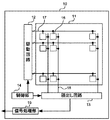
図1は本発明の第1実施形態に係る撮像装置10の構成例を説明する。撮像装置10は、画素アレイ11、駆動回路12、読出し回路13、制御部14及び信号処理部15を備えうる。画素アレイ11には、入射光に応じた信号を出力する画素16がアレイ状に配置される。駆動回路12は制御部14からの指示に従って、駆動線17を介して行ごとに画素16に制御信号を供給する。読出し回路13は制御部14からの指示に従って、画素16から信号線18に出力された信号を列ごとに読み出し、信号処理部15に出力する。信号処理部15はそれぞれの画素16から出力された信号に基づいて各画素16の画素値を決定する。
<First Embodiment>
FIG. 1 illustrates a configuration example of an
図2は、図1の画素16の一例である画素20の回路構成例を説明する。画素20は、空乏型のフォトダイオードPD及びスイッチ21を備えうる。フォトダイオードPDは入射光に応じた電荷を発生する光電変換部として機能する。フォトダイオードPDのアソードは接地GNDに接続され、カソードはスイッチ21を介して電圧源VRESに接続される。スイッチ21が導通状態(オン)になると、フォトダイオードPDは電圧源VRESから供給されるリセット電圧Vresによって逆バイアスに設定され、フォトダイオードPDの少なくとも一部が空乏化される。すなわち、スイッチ21はフォトダイオードPDをリセットするリセット部として機能する。リセット電圧VresによってフォトダイオードPDの全体が空乏化されてもよい。フォトダイオードPDがリセットされた後、フォトダイオードPDに光が照射されて電荷が発生すると、この逆バイアスが緩和され、空乏化していた領域に電荷が蓄積される。
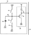
FIG. 2 illustrates a circuit configuration example of the
画素20はさらに、スイッチ22とコンデンサ23とを備えうる。コンデンサ23は一方の電極(図2では下側の電極)が接地GNDに接続され、他方の電極(図2では上側の電極)がスイッチ22を介してフォトダイオードPDのカソードに接続される。スイッチ22が導通状態になると、コンデンサ23とフォトダイオードPDのカソードが接続されて、コンデンサ23の容量値がフォトダイオードPDの容量値に付加される。すなわち、スイッチ22はコンデンサ23をフォトダイオードPDに接続する接続部として機能する。スイッチ21及びスイッチ22には駆動回路12から駆動線17を介して制御信号がそれぞれ供給される。
The
画素20はさらに、定電流源24とトランジスタ25とを有するソースフォロア回路SFを備えうる。トランジスタ25のゲートはフォトダイオードPDのカソードに接続される。ソースフォロア回路SFは高インピーダンス入力のアンプの一種であり、フォトダイオードPDに蓄積された電荷に基づく信号を増幅して信号線18に出力する。具体的には、ソースフォロア回路SFは、ソースフォロア回路SFとフォトダイオードPDとを接続するノードNDの電位に基づく信号を出力する。このように、ソースフォロア回路SFは、フォトダイオードPDに電気的に接続されたノードNDの電位に基づく信号を出力する出力部として機能する。このノードNDの電位は、ソースフォロア回路SFの入力ノード(トランジスタ25のゲート)の電位及びフォトダイオードPDのカソードの電位のそれぞれに等しいと見なすことができる。
The
次に、図3を参照しつつ、図2のフォトダイオードPDの断面構造例について説明する。図3は図2の画素20のうちフォトダイオードPDに着目した図である。図3では、フォトダイオードPDに蓄積される信号電荷が電子である場合を説明するが、各半導体領域の導電型を反対にして、正孔を信号電荷として用いてもよい。
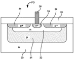
Next, an example of a cross-sectional structure of the photodiode PD in FIG. 2 will be described with reference to FIG. FIG. 3 is a diagram focusing on the photodiode PD in the
n型の半導体基板30にp型のウェル領域(半導体領域)31が形成されており、このウェル領域31に入射した光に応じて電子が発生する。ウェル領域31にn型の半導体領域32が形成される。半導体領域32の中央部にn型の半導体領域33が形成される。半導体領域33は半導体領域32よりも不純物濃度が高い。半導体基板30の表面にはp型の半導体領域34が形成されており、半導体基板30の表面が空乏化しないように半導体領域34はウェル領域31よりも不純物濃度が高い。半導体基板30の表面は酸化膜などの絶縁層35で覆われている。半導体領域33は絶縁層35を貫通するコンタクトプラグ36を介して図2のソースフォロア回路SFに接続される。スイッチ21が非導通状態(オフ)の場合に半導体領域33は電気的にフローティング状態となる。そこで、半導体領域33をフローティングディフュージョンと呼んでもよい。
A p-type well region (semiconductor region) 31 is formed in the n-
半導体領域32の不純物濃度は例えば1×1015〜5×10¹⁷(cm-2)程度である。半導体領域33の不純物濃度は例えば1×10¹⁸〜5×10²⁰(cm-2)程度である。半導体領域34の不純物濃度は例えば1×10¹⁷〜5×10²⁰(cm-2)程度である。このような不純物濃度の分布により、フォトダイオードPDで発生した電子は半導体領域33に収集され、そこに先に蓄積される。そして、半導体領域33が飽和した場合に、電子は続いて半導体領域32に蓄積される。また、不純物濃度の高い半導体領域33の方が半導体領域32よりも単位体積あたりの空乏化電圧が高い。その結果、同量の電荷(この例では電子)が蓄積した場合に、半導体領域33に蓄積した場合の方が、半導体領域32に蓄積した場合よりも、ノードNDの電位の変化量が大きくなる。言い換えると、半導体領域33に所定量の電荷が蓄積したことによるノードNDの電位変化は、半導体領域33に電荷が蓄積したことによるノードNDの電位変化よりも敏感である。例えば、一定の光量の光が同じ時間だけ照射された場合に、同量の電荷が蓄積される。本実施形態では、半導体領域33(第1部分)及び半導体領域32(第2部分)が電荷蓄積領域として機能する。
The impurity concentration of the
次に、図4を参照して撮像装置10の制御方法の一例を説明する。図4(a)はこの制御方法におけるタイミングチャートであり、図4(b)、(c)はタイミングチャートの各時刻におけるノードNDの電位を示すグラフである。図4(b)は画素20への入射光が低照度の場合を示し、図4(c)は画素20への入射光が高照度の場合を示す。図4(b)、(c)では横軸に時刻をとり、縦軸にノードNDの電位をとる。この図では縦軸上向きを正とする。このタイミングチャートで説明される制御方法は撮像装置10の駆動回路12が画素20内のスイッチ21、22に制御信号を供給することによって実行される。図4では1つの画素20から信号を読み出す場合を説明するが、同様の制御方法が画素アレイ11内の他の画素について行われてもよい。以下に説明する他の実施形態の制御方法についても同様である。
Next, an example of a method for controlling the
時刻t1において、駆動回路12はスイッチ21に供給する制御信号をローレベルからハイレベルに切り替え、スイッチ21を導通状態にする。また、時刻t1において、駆動回路12がスイッチ22に供給する制御信号はハイレベルであり、スイッチ22は導通状態である。従って、時刻t1において、ノードNDの電位がリセット電圧Vresにリセットされるとともに、コンデンサ23の電位もリセット電圧Vresにリセットされる。時刻t2において、駆動回路12がスイッチ22に供給する制御信号をローレベルに切り替えて、スイッチ22を非導通状態にすると、コンデンサ23がフォトダイオードPDから切断される。
At time t1, the
時刻t3において、駆動回路12がスイッチ21に供給する制御信号をローレベルに切り替えて、スイッチ21を非導通状態にすると、ノードNDがフローティング状態になる。それにより、フォトダイオードPDで発生した電荷が半導体領域33に蓄積され始め、電荷の蓄積期間が始まる。すなわち、撮像装置の駆動回路12は、画素20の電荷蓄積期間の開始時刻t3になると、スイッチ21に供給する制御信号をローレベルに切り替える。本実施形態では蓄積される電荷が電子であるので、電荷が蓄積するにつれてノードNDの電位が下がる。
At time t3, when the control signal supplied to the
ここで、図5を参照しつつ、電荷蓄積期間におけるノードNDの電位の変化について説明する。図5(a)は時刻t3における電荷蓄積期間の開始時点の状態を示す模式図であり、図5(b)は半導体領域33が飽和する前の状態を示す模式図であり、図5(b)は半導体領域33が飽和した後の状態を示す模式図である。各図において、縦軸はノードNDの電位を示し、下向きを正とする。また、ハッチング部分の面積がフォトダイオードPDに蓄積された電荷量Qに相当する。Vcurは各時刻におけるノードNDの電位を示し、Vsatは半導体領域33が飽和した時点のノードNDの電位を示す。前述の通り、電荷蓄積期間中は、コンデンサ23がノードNDから切り離されている。そのため、ノードNDの電位は、フォトダイオードPDで発生した電荷量とフォトダイオードPDの容量とに依存する。
Here, a change in the potential of the node ND in the charge accumulation period will be described with reference to FIG. FIG. 5A is a schematic diagram illustrating a state at the start of the charge accumulation period at time t3, and FIG. 5B is a schematic diagram illustrating a state before the
図5(a)は、スイッチ21を導通状態とし、ノードNDに電圧源VRESを接続した状態を示す。この場合に、ノードNDは電圧源VRESによって供給されるリセット電圧Vresに等しくなる。続いて、スイッチ21を非導通状態とし、ノードNDがフローティング状態になると、フォトダイオードPDで発生した電子は半導体領域33に蓄積され、図5(b)に示されるようにノードNDの電位が下がる。半導体領域33の容量値をCfとすると、半導体領域33が飽和するまでの間、すなわちVres≧Vcur≧Vsatを満たす間、以下の関係が成り立つ。
Vres−Vcur=Q/Cf
このように、半導体領域33が飽和するまでの間、ノードNDの電位変化量(すなわち、Vres−Vcur)は蓄積された電荷量Qに対して比例して変化する。
FIG. 5A shows a state in which the
Vres−Vcur = Q / Cf
Thus, the potential change amount (ie, Vres−Vcur) of the node ND changes in proportion to the accumulated charge amount Q until the
蓄積された電荷量Qが増加し、半導体領域33が飽和すると、電荷は半導体領域32に蓄積され始める。半導体領域32の容量値は半導体領域33の容量値Cfよりも大きいので、図5(c)に示されるように、ノードNDの電位Vcurは緩やかに変化するようになる。ノードNDの電位Vcurの変化率がどの程度低下するかは、半導体領域33と半導体領域32との面積比に依存する。面積比が大きいほど、変化率の低下も大きくなるとともに、より多くの電荷をフォトダイオードPDに蓄積できる。これにより、フォトダイオードPDのダイナミックレンジを向上できる。
When the accumulated charge amount Q increases and the
再び図4を参照して、時刻t4において、電荷蓄積期間が終了すると、読出し回路13は画素20のソースフォロア回路SFが信号線18に出力している信号を読み出して、信号処理部15に出力する。ソースフォロア回路SFによる信号の出力動作は、例えば、後段のメモリに信号を保持することや、後段のサンプルホールドスイッチをオンすることによってなされる。サンプルホールドスイッチは、ソースフォロア回路SFと、後段の回路、例えばメモリやアンプとを接続するスイッチである。ソースフォロア回路SFが出力する信号は時刻t4におけるノードNDの電位に相当する信号である。時刻t5において、駆動回路12はスイッチ22に供給する制御信号をハイレベルに切り替えて、スイッチ22を導通状態にする。これにより、コンデンサ23がノードNDに接続され、ノードNDの電位が変化する。このとき、フォトダイオードPDに蓄積された電荷がコンデンサ23に分配されることにより、ノードNDの電位が変化しうる。その後、時刻t6において、読出し回路13は画素20のソースフォロア回路SFが信号線18に出力している信号を再度読み出して、信号処理部15に出力する。ソースフォロア回路SFが出力する信号は時刻t6におけるノードNDの電位に相当する信号である。本実施例では、時刻t6において、スイッチ22が導通状態、つまり、フォトダイオードPDにコンデンサ23が接続された状態で信号を読み出している。しかし、時刻t6において、スイッチ22を非導通状態として信号を読み出してもよい。スイッチ22が導通状態になることにより電荷が分配されるため、一度スイッチ22が導通状態になった後であれば、スイッチ22を非導通状態としても電位が保たれるからである。
Referring to FIG. 4 again, when the charge accumulation period ends at time t4, the
次に、時刻t4、t6においてソースフォロア回路SFが出力する2つの信号について説明する。ノードNDの電位のVresからの変化量(Vres−Vcur)は、画素20に蓄積された電荷量をノードNDの容量値で割った値で与えられる。時刻t6ではコンデンサ23の容量値がノードNDに付加されているので、電荷量Qに対するノードNDの電位の変化率(ゲイン)は時刻t4よりも時刻t6の方が小さい。そこで、以下では時刻t4においてソースフォロア回路SFが出力する信号を高ゲイン信号(第1信号)と呼び、時刻t6においてソースフォロア回路SFが出力する信号を低ゲイン信号(第2信号)と呼ぶ。また、コンデンサ23がノードNDに接続されていない状態を高ゲイン状態と呼び、コンデンサ23がノードNDに接続されている状態を低ゲイン状態と呼ぶ。
Next, two signals output from the source follower circuit SF at times t4 and t6 will be described. A change amount (Vres−Vcur) of the potential of the node ND from Vres is given by a value obtained by dividing the amount of charge accumulated in the
スイッチ22が導通状態となり、高ゲイン状態から低ゲイン状態に移行した場合に、半導体領域33及び場合によっては半導体領域32に蓄積された電荷はコンデンサ23に分配される。この場合でも、電子の再結合は発生せず、フォトダイオードPDで発生し蓄積された電荷の電荷量Qは保存されたままである。そのため、コンデンサ23の容量をCsとすると、以下の関係が成り立つ。
Vres−Vcur=Q/(Cf+Cs)
このようにノードNDにコンデンサ23の容量を付加することによって、図4(c)に示されるように、入射光の照度が高く、高ゲイン状態において線形関係を満たさないような電荷量Qであっても、低ゲイン状態で測定した場合には線形関係を満たしうる。
When the
Vres−Vcur = Q / (Cf + Cs)
By adding the capacitance of the
図6に、本実施形態の撮像装置10で測定した実験結果を示す。図6のグラフの横軸は蓄積期間を表す。蓄積される電荷量Qは蓄積期間に比例する。図6のグラフの縦軸はソースフォロア回路SFから出力される出力信号の値を表す。この実験では、半導体領域33の容量値を約5fFとし、コンデンサ23の容量値を約20fFとした場合に、低ゲイン状態及び高ゲイン状態のそれぞれについて蓄積期間と出力信号との関係をプロットした。この実験結果からわかるように、低ゲイン状態及び高ゲイン状態のいずれにおいても、良好な線形性が得られた。また、高ゲイン状態では飽和して線形性が得られない電荷量Qに対しても、低ゲイン状態では線形性が得られている。図6に示すグラフでは、低ゲイン状態と高ゲイン状態との感度比は約5倍である。半導体領域33とコンデンサ23の容量比が大きいほど、高ゲイン状態において線形性が得られる範囲が広がる。発明者の実験では、約30倍までの線形性が確認できた。
FIG. 6 shows experimental results measured by the
本実施形態において、電荷蓄積期間(時刻t3から時刻t4までの期間)は撮像条件によって定まる設計値である。電荷蓄積期間終了後(時刻t4以降)においてもフォトダイオードPDで電荷が発生し、半導体領域33又は半導体領域32に電荷が蓄積する。しかし、読出し時間を短くして時刻t4と時刻t6と間を短くすれば、ほぼ同じ電荷量Qについて低ゲイン信号と高ゲイン信号との両方が信号処理部15に出力される。例えば、時刻t4及び時刻t6からそれぞれ開始される読出し時間は例えば10マイクロ秒以下にできる。
In the present embodiment, the charge accumulation period (period from time t3 to time t4) is a design value determined by the imaging conditions. Even after the end of the charge accumulation period (after time t4), charges are generated in the photodiode PD, and the charges are accumulated in the
信号処理部15は、読出し回路13から出力された信号の値に基づいて、どちらの信号に基づいて画素値を決定するかを判定する。例えば、信号処理部15は、図4に示される信号の値が所定の値よりも小さければ低ゲイン信号を用いて画素20の画素値を決定し、それ以外の場合に高ゲイン信号を用いて画素値を決定してもよい。この所定の値として、ノードNDの電位が飽和電圧Vsatに等しい場合にソースフォロア回路SFから出力される信号の値としてもよい。また、飽和電圧Vsatが画素ごとにばらつきうることを考慮して、ノードNDの電位が飽和電圧Vsatに等しい場合にソースフォロア回路SFから出力される信号の値にオフセットを追加してもよい。これにより、飽和電圧Vsatが画素ごとにばらついたとしても、画素20からの信号を線形に取得でき、撮像装置10で得られる画像の画質が向上する。
Based on the value of the signal output from the
感度の異なる複数の部分を含む電荷蓄積領域を形成する方法として、上述のように半導体領域32と半導体領域33とで不純物濃度を異ならせてもよい。また、PN接合するp型の半導体領域34の不純物濃度を異ならせてもよい。図3に示されるように、フォトダイオードPDを形成するPN接合のn型半導体領域は、基板表面のp型の半導体領域34が配された部分と配されていない部分とで、電荷が蓄積された場合のノードNDの電位変化が異なる。
As a method for forming a charge storage region including a plurality of portions having different sensitivities, the impurity concentration may be different between the
<第2実施形態>
続いて、図7を参照して本発明の第2実施形態について説明する。図7(a)は本実施形態の画素70の構成を説明する回路図であり、図7(b)はこの画素70を含む撮像装置10の制御方法の一例を説明するタイミングチャートである。本実施形態では、図1の撮像装置10の画素16として、図7(a)に示される画素70を用いる。図2の画素20と図7の画素70とで共通する構成要素には同一の参照符号を付して重複する説明を省略する。
Second Embodiment
Subsequently, a second embodiment of the present invention will be described with reference to FIG. FIG. 7A is a circuit diagram illustrating the configuration of the
画素70は、サンプルホールド回路(SH回路)71H、71Lと、出力アンプ72H、72Lとを備える点で画素20とは異なる。また、撮像装置10の信号線18は信号線18H、18Lを含む。SH回路71H(第1保持部)はソースフォロア回路SFから出力された高ゲイン信号を保持し、SH回路71L(第2保持部)はソースフォロア回路SFから出力された低ゲイン信号を保持する。SH回路71H、71Lは、それぞれサンプルホールドスイッチと信号保持容量とを含んで構成されうる。出力アンプ72HはSH回路71Hの保持する信号を信号線18Hに出力し、出力アンプ72LはSH回路71Lの保持する信号を信号線18Lに出力する。
The
続いて、本実施形態における撮像装置10の制御方法の一例を説明する。タイミングチャートの各時刻におけるノードNDの電位を示すグラフは図4(b)、(c)と同一であるため省略する。このタイミングチャートで説明される制御方法は撮像装置10の駆動回路12が画素70内のスイッチ21、22及びSH回路71H、71Lに制御信号を供給することによって実行される。
Next, an example of a method for controlling the
時刻t1、t2、t3、t5における動作は第1実施形態と同じであるため、重複する説明を省略する。時刻t4で電荷蓄積期間が終了すると、駆動回路12はSH回路71Hへ供給される制御信号を一定期間だけハイレベルに切り替える。これによって、ソースフォロア回路SFから出力されている高ゲイン信号がSH回路71Hに保持される。時刻t6で、駆動回路12はSH回路71Lへ供給される制御信号を一定期間だけハイレベルに切り替える。これによって、ソースフォロア回路SFから出力されている低ゲイン信号がSH回路71Lに保持される。その後、読出し回路13は信号線18H、18Lのそれぞれから信号を読み出して、信号処理部15へ出力する。
Since the operations at times t1, t2, t3, and t5 are the same as those in the first embodiment, a duplicate description is omitted. When the charge accumulation period ends at time t4, the
本実施形態も第1実施形態と同じ効果が得られる。また、第1実施形態では、読出し回路13は画素アレイ11の各列に対応するすべての信号線18から高ゲイン信号を読み出し、その後に低ゲイン信号を読み出す必要があった。しかし、本実施形態では、各画素70において並行して高ゲイン信号と低ゲイン信号とをSH回路71H、71Lに保持し、その後に読出し回路13がこれらの信号を読み出せばよい。そのため、時刻t3と時刻t5との間を短縮できる。
This embodiment can also obtain the same effect as the first embodiment. In the first embodiment, the
<第3実施形態>
続いて、図8を参照して本発明の第3実施形態について説明する。図8(a)は本実施形態の画素80の構成を説明する回路図であり、図8(b)はこの画素80を含む撮像装置10の制御方法の一例を説明するタイミングチャートである。本実施形態では、図1の撮像装置10の画素16として、図8(a)に示される画素80を用いる。図7の画素70と図8の画素80とで共通する構成要素には同一の参照符号を付して重複する説明を省略する。
<Third Embodiment>
Next, a third embodiment of the present invention will be described with reference to FIG. FIG. 8A is a circuit diagram illustrating the configuration of the
画素80は、SH回路71Rと出力アンプ72Rとを更に備える点で画素70とは異なる。また、撮像装置10の信号線18は信号線18H、18L、18Rを含む。SH回路71Rはソースフォロア回路SFから出力されたリセット時の信号を保持する。出力アンプ72RはSH回路71Rの保持する信号を信号線18Rに出力する。
The
続いて、本実施形態における撮像装置10の制御方法の一例を説明する。タイミングチャートの各時刻におけるノードNDの電位を示すグラフは図4(b)、(c)と同一であるため省略する。このタイミングチャートで説明される制御方法は撮像装置10の駆動回路12が画素70内のスイッチ21、22及びSH回路71H、71L、71Rに制御信号を供給することによって実行される。
Next, an example of a method for controlling the
時刻t1、t2、t4〜t6における動作は第2実施形態と同じであるため、重複する説明を省略する。時刻t3で、電荷蓄積期間が開始されると、駆動回路12は、上述のようにスイッチ21へ供給する制御信号をローレベルに切り替えると共に、SH回路71Rへ供給される制御信号を一定期間だけハイレベルに切り替える。これによって、ソースフォロア回路SFから出力されている電荷蓄積期間開始直後の信号(以下、リセット信号)がSH回路71Rに保持される。時刻t6の後、読出し回路13は信号線18H、18L、18Rのそれぞれから信号を読み出して、信号処理部15へ出力する。信号処理部15は、高ゲイン信号を用いて画素値を決定する場合に、高ゲイン信号からリセット信号(第3信号)を減算し、その値に基づいて画素値を決定する。これによって、フォトダイオードPDのリセット時に発生するKTCノイズやランダムノイズを除去することができる。ランダムノイズはリセットされる容量が小さいほど大きな電圧となるので、高ゲイン信号からリセット信号を減算することは特に効果がある。また、信号処理部15は低ゲイン信号を用いて画素値を決定する場合に、低ゲイン信号からリセット信号を減算し、その値に基づいて画素値を決定してもよい。また、画素80は期間t1〜t2の間にコンデンサ23がノードNDに接続された状態でソースフォロア回路SFから出力される信号を保持するためのSH回路を更に有してもよい。信号処理部15は上述のリセット信号の代わりにこの信号を低ゲイン信号から減算してもよい。
Since the operations at times t1, t2, and t4 to t6 are the same as those in the second embodiment, a duplicate description is omitted. When the charge accumulation period starts at time t3, the
<第4実施形態>
続いて、図9、図10を参照して本発明の第4実施形態について説明する。上述の第1実施形態において、蓄積された電荷量Qが多い場合に、低ゲイン状態においてもノードNDの電位が飽和電圧Vsatを超えてしまい、低ゲイン信号の線形性を維持できないことがある。このような場合に、コンデンサ23の容量を大きくして線形性を維持しようとすると、高ゲイン状態において飽和電圧Vsatを若干上回るような電荷量Qを十分な感度で測定できなくなる。そこで、本実施形態では、2段階に分けてノードNDに容量値を付加する。図9は本実施形態の画素90の構成を説明する回路図である。本実施形態では、図1の撮像装置10の画素16として、図9に示される画素90を用いる。図8の画素80と図9の画素90とで共通する構成要素には同一の参照符号を付して重複する説明を省略する。
<Fourth embodiment>
Next, a fourth embodiment of the present invention will be described with reference to FIGS. In the first embodiment described above, when the accumulated charge amount Q is large, the potential of the node ND may exceed the saturation voltage Vsat even in the low gain state, and the linearity of the low gain signal may not be maintained. In such a case, if it is attempted to maintain the linearity by increasing the capacitance of the
画素90は、スイッチ22及びコンデンサ23の代わりにスイッチ22a、22b及びコンデンサ23a、23bを有し、SH回路71M(第3保持部)及び出力アンプ72Mを更に有する点で画素80とは異なる。また、撮像装置10の信号線18は信号線18H、18M、18L、18Rを含む。スイッチ22a及びコンデンサ23aはスイッチ22及びコンデンサ23と同様の構成であり、スイッチ22b及びコンデンサ23bもスイッチ22及びコンデンサ23と同様の構成である。SH回路71Mはソースフォロア回路SFから出力された信号を保持する。出力アンプ72MはSH回路71Mの保持する信号を信号線18Mに出力する。
The
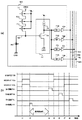
図10(a)はこの画素90を含む撮像装置10の制御方法の一例を説明するタイミングチャートであり、図10(b)はノードNDの電位を説明する図である。時刻t1〜t3における動作は第3実施形態と同じであるため、重複する説明を省略する。ただし、時刻t2において、スイッチ22が非導通状態に切り替わる代わりに、スイッチ22a、22bが非導通状態に切り替わる。時刻t4で、電荷蓄積期間が終了すると、駆動回路12は、SH回路71Hへ供給される制御信号を一定期間だけハイレベルに切り替える。これによって、ソースフォロア回路SFから出力されている信号(高ゲイン信号)がSH回路71Hに保持される。時刻t5において、駆動回路12はスイッチ22aに供給する制御信号をハイレベルに切り替えて、スイッチ22aを導通状態にする。これにより、コンデンサ23aがノードNDに接続され、ノードNDの電位は変化する。図10(b)に示されるように、コンデンサ23aの容量値をノードNDに付加しても、ノードNDの電位は飽和電圧Vsatを下回ったままである。時刻t6において、駆動回路12は、SH回路71Mへ供給される制御信号を一定期間だけハイレベルに切り替える。これによって、ソースフォロア回路SFから出力されている信号(中ゲイン信号)がSH回路71Mに保持される。時刻t7において、駆動回路12はスイッチ22bに供給する制御信号をハイレベルに切り替えて、スイッチ22bを導通状態にする。これにより、コンデンサ23bがノードNDに接続され、ノードNDの電位は変化する。時刻t8において、駆動回路12は、SH回路71Lへ供給される制御信号を一定期間だけハイレベルに切り替える。これによって、ソースフォロア回路SFから出力されている信号(低ゲイン信号)がSH回路71Lに保持される。
FIG. 10A is a timing chart for explaining an example of a control method for the
その後、読出し回路13は信号線18H、18M18L、18Rのそれぞれから信号を読み出して、信号処理部15へ出力する。信号処理部15は、高ゲイン信号、中ゲイン信号、低ゲイン信号の何れかと、リセット信号とを用いて画素値を決定する。信号処理部15は、時刻t4におけるノードNDの電位Vt4がVt4>Vsatを満たすならば低ゲイン信号を用いて画素20の画素値を決定する。それ以外の場合に、信号処理部15は、時刻t6におけるノードNDの電位Vt6がVt6>Vsatを満たすならば中ゲイン信号を用いて画素値を決定し、それ以外の場合に高ゲイン信号を用いて画素値を決定してもよい。また、飽和電圧Vsatが画素ごとにばらつきうることを考慮して、第1実施形態と同様に飽和電圧Vsatにオフセットを追加してもよい。本実施形態では、ノードNDへ付加する容量を2段階に切り替えたが、3段階以上に切り替えることも可能である。
Thereafter, the
<第5実施形態>
続いて、図11を参照して本発明の第5実施形態について説明する。図11(a)は本実施形態の画素110の構成を説明する回路図であり、図11(b)はこの画素110を含む撮像装置10の制御方法の一例を説明するタイミングチャートである。本実施形態では、図1の撮像装置10の画素16として、図11(a)に示される画素110を用いる。図2の画素20と図11の画素110とで共通する構成要素には同一の参照符号を付して重複する説明を省略する。画素110は、スイッチ21、22及びコンデンサ23の代わりに、MOSトランジスタ(MOSFET)TR、TCを備える点で画素20とは異なる。MOSトランジスタTR、TCは電圧源VRESとノードNDとの間に直列に接続される。
<Fifth Embodiment>
Next, a fifth embodiment of the present invention will be described with reference to FIG. FIG. 11A is a circuit diagram illustrating the configuration of the
続いて、本実施形態における撮像装置10の制御方法の一例を説明する。タイミングチャートの各時刻におけるノードNDの電位を示すグラフは図4(b)、(c)と同一であるため省略する。このタイミングチャートで説明される制御方法は撮像装置10の駆動回路12が画素110内のMOSトランジスタTR、TCのゲートに制御信号を供給することによって実行される。
Next, an example of a method for controlling the
時刻t1において、駆動回路12はMOSトランジスタTCに供給する制御信号をローレベルからハイレベルに切り替え、MOSトランジスタTCを導通状態にする。また、時刻t1において、駆動回路12がMOSトランジスタTRに供給する制御信号はハイレベルであり、MOSトランジスタTRは導通状態である。従って、時刻t1において、ノードNDの電位がリセット電圧Vresにリセットされる。このように、MOSトランジスタTC、TRは一緒になってリセット部として機能する。
At time t1, the
時刻t3において、駆動回路12がMOSトランジスタTCに供給する制御信号をローレベルに切り替えて、MOSトランジスタTCを非導通状態にすると、ノードNDがフローティング状態になる。従って、フォトダイオードPDで発生した電荷が半導体領域33に蓄積され始め、電荷の蓄積期間が始まる。すなわち、撮像装置の駆動回路12は、画素20の電荷蓄積期間の開始時刻t3になると、MOSトランジスタTCに供給する制御信号をローレベルに切り替える。本実施形態でも蓄積される電荷が電子であるので、電荷が蓄積するにつれてノードNDの電位が下がる。
At time t3, when the control signal supplied from the
時刻t4において、電荷蓄積期間が終了すると、読出し回路13は画素20のソースフォロア回路SFが信号線18に出力している信号を読み出して、信号処理部15に出力する。ソースフォロア回路SFが出力する信号は時刻t4におけるノードNDの電位に相当する信号(高ゲイン信号)である。時刻t5において、駆動回路12はMOSトランジスタTRに供給する制御信号をローレベルに切り替えて、MOSトランジスタTRを非導通状態にする。これと同時に、またはこの後に、駆動回路12は、MOSトランジスタTCに供給する制御信号をハイレベルに切り替えて、MOSトランジスタTCを導通状態にする。これにより、MOSトランジスタTCの容量値がノードNDに付加され、ノードNDの電位は変化する。従って、MOSトランジスタTCは容量をノードNDに接続する接続部として機能する。その後、時刻t6において、読出し回路13は画素20のソースフォロア回路SFが信号線18に出力している信号を再度読み出して、信号処理部15に出力する。ソースフォロア回路SFが出力する信号は時刻t6におけるノードNDの電位に相当する信号(低ゲイン信号)である。
When the charge accumulation period ends at time t4, the
本実施形態も第1実施形態と同じ効果が得られる。さらに、本実施形態ではスイッチとしてMOSトランジスタTCだけがノードNDに接続されるため、ノードNDの容量を低減できる。本実施形態でも、上述の第2実施形態や第3実施形態と同様に各画素がソースフォロア回路SFからの出力を保持するSF回路を有してもよい。 This embodiment can also obtain the same effect as the first embodiment. Furthermore, in this embodiment, only the MOS transistor TC as a switch is connected to the node ND, so that the capacity of the node ND can be reduced. Also in this embodiment, each pixel may have an SF circuit that holds the output from the source follower circuit SF, as in the second and third embodiments described above.
<第6実施形態>
続いて、図12を参照して本発明の第6実施形態について説明する。図12(a)は本実施形態の画素120の構成を説明する回路図であり、図12(b)はこの画素120を含む撮像装置10の制御方法の一例を説明するタイミングチャートである。本実施形態では、図1の撮像装置10の画素16として、図12(a)に示される画素120を用いる。図9の画素90と図12の画素120とで共通する構成要素には同一の参照符号を付して重複する説明を省略する。本実施形態においても、上述の第4実施形態と同様に、2段階に分けてノードNDに容量値を付加する。画素120は、スイッチ21、22a、22b及びコンデンサ23a、23bの代わりに、MOSトランジスタTR、TCa、TCbを備える点で画素90とは異なる。MOSトランジスタTR、TCa、TCbは電圧源VRESとノードNDとの間に直列に接続される。
<Sixth Embodiment>
Subsequently, a sixth embodiment of the present invention will be described with reference to FIG. FIG. 12A is a circuit diagram illustrating the configuration of the
続いて、本実施形態における撮像装置10の制御方法の一例を説明する。タイミングチャートの各時刻におけるノードNDの電位を示すグラフは図10(b)と同一であるため省略する。このタイミングチャートで説明される制御方法は撮像装置10の駆動回路12が画素120内のMOSトランジスタTR、TCa、TCbのゲートに制御信号を供給することによって実行される。
Next, an example of a method for controlling the
時刻t1、t3における動作は第5実施形態と同じであるため、重複する説明を省略する。ただし、時刻t3において、駆動回路12はMOSトランジスタTCa、TCbに供給する制御信号をローレベルに切り替える。時刻t5において、駆動回路12はMOSトランジスタTRに供給する制御信号をローレベルに切り替えて、MOSトランジスタTRを非導通状態にする。これと同時に、またはこの後に、MOSトランジスタTCaに供給する制御信号をハイレベルに切り替えて、MOSトランジスタTCaを導通状態にする。これにより、MOSトランジスタTCaの容量値がノードNDに付加され、ノードNDの電位は変化する。時刻t7において、駆動回路12は、MOSトランジスタTCbに供給する制御信号をハイレベルに切り替えて、MOSトランジスタTCbを導通状態にする。これにより、MOSトランジスタTCbの容量値もノードNDに付加され、ノードNDの電位は変化する。このように、本実施形態ではノードNBに2段階で容量値が付加される。本実施形態でも、4つ以上のMOSトランジスタを電圧源VRESとノードNDとの間に接続して、3段階以上でノードNBに容量値を付加してもよい。
Since the operations at times t1 and t3 are the same as those in the fifth embodiment, a duplicate description is omitted. However, at time t3, the
Claims (7)
前記複数の画素のそれぞれは、
電荷蓄積領域を有する光電変換部と、
前記電荷蓄積領域に接続されたコンタクトプラグを含むノードの電位に基づいて信号を出力する出力部と、
前記ノードに容量を電気的に接続する接続部とを含み、
前記電荷蓄積領域は第1部分及び第2部分を含み、光電変換により発生した電荷は前記第1部分に先に蓄積され、前記第1部分が飽和した後に前記第2部分に蓄積され、
前記ノードに前記容量が電気的に接続された状態で前記第1部分と前記容量とに所定量の電荷が分散して蓄積されたことによる前記ノードの電位変化の量は、前記ノードに前記容量が電気的に接続されていない状態で前記第1部分に前記所定量の電荷が蓄積されたことによる前記ノードの電位変化の量よりも小さく、前記ノードに前記容量が電気的に接続されていない状態で前記第2部分に前記所定量の電荷が蓄積されたことによる前記ノードの電位変化の量よりも大きく、
前記出力部は、前記ノードに前記容量が電気的に接続されていない状態で前記電荷蓄積領域への信号電荷の蓄積が開始された後に、前記容量が電気的に接続される前の前記ノードの前記信号電荷に応じた電位に基づいて第1信号を出力し、その後に前記容量が電気的に接続された後の前記ノードの前記信号電荷に応じた電位に基づいて第2信号を出力することを特徴とする撮像装置。 An imaging device having a plurality of pixels,
Each of the plurality of pixels is
A photoelectric conversion unit having a charge storage region;
An output unit that outputs a signal based on a potential of a node including a contact plug connected to the charge storage region;
A connection part for electrically connecting a capacity to the node;
The charge accumulation region includes a first part and a second part, and the charge generated by photoelectric conversion is accumulated in the first part first, and after the first part is saturated, is accumulated in the second part,
The amount of change in the potential of the node due to a predetermined amount of electric charge being distributed and accumulated in the first portion and the capacitor in a state where the capacitor is electrically connected to the node is determined by the capacitance at the node. Is smaller than the amount of change in potential of the node due to the accumulation of the predetermined amount of charge in the first portion in a state where the capacitor is not electrically connected, and the capacitor is not electrically connected to the node Larger than the amount of potential change of the node due to the accumulation of the predetermined amount of charge in the second portion in the state,
The output unit starts the accumulation of the signal charge in the charge accumulation region in a state where the capacitor is not electrically connected to the node, and before the capacitor is electrically connected. Outputting a first signal based on a potential corresponding to the signal charge, and then outputting a second signal based on a potential corresponding to the signal charge of the node after the capacitor is electrically connected. An imaging apparatus characterized by the above.
前記第1部分は、前記第2部分に取り囲まれることを特徴とする請求項1に記載の撮像装置。 The contact plug is connected to the first portion;
The imaging apparatus according to claim 1, wherein the first part is surrounded by the second part.
前記処理部は、前記第1信号の値が所定の値よりも小さい場合に、前記第1信号に基づいて前記画素値を決定し、前記第1信号の値が前記所定の値よりも大きい場合に、前記第2信号に基づいて前記画素値を決定することを特徴とする請求項1又は2に記載の撮像装置。 The imaging apparatus further includes a processing unit that determines a pixel value using a signal output from the output unit,
The processing unit determines the pixel value based on the first signal when the value of the first signal is smaller than a predetermined value, and the value of the first signal is larger than the predetermined value The imaging apparatus according to claim 1, wherein the pixel value is determined based on the second signal.
前記ノードの電位をリセット電圧に設定するリセット部と、
前記ノードの電位が前記リセット電圧に設定された状態で前記出力部が前記ノードの電位に基づいて出力する第3信号を保持する第3保持部とを更に含むことを特徴とする請求項5に記載の撮像装置。 Each of the plurality of pixels is
A reset unit for setting the potential of the node to a reset voltage;
The third holding unit that holds a third signal that the output unit outputs based on the potential of the node in a state where the potential of the node is set to the reset voltage. The imaging device described.
Priority Applications (3)
| Application Number | Priority Date | Filing Date | Title |
|---|---|---|---|
| JP2012183583A JP6077786B2 (en) | 2012-08-22 | 2012-08-22 | Imaging device |
| US13/957,737 US9257460B2 (en) | 2012-08-22 | 2013-08-02 | Image capturing apparatus and control method therefor |
| US14/946,911 US9362326B2 (en) | 2012-08-22 | 2015-11-20 | Image capturing apparatus and control method therefor |
Applications Claiming Priority (1)
| Application Number | Priority Date | Filing Date | Title |
|---|---|---|---|
| JP2012183583A JP6077786B2 (en) | 2012-08-22 | 2012-08-22 | Imaging device |
Publications (3)
| Publication Number | Publication Date |
|---|---|
| JP2014042167A JP2014042167A (en) | 2014-03-06 |
| JP2014042167A5 JP2014042167A5 (en) | 2015-06-25 |
| JP6077786B2 true JP6077786B2 (en) | 2017-02-08 |
Family
ID=50147149
Family Applications (1)
| Application Number | Title | Priority Date | Filing Date |
|---|---|---|---|
| JP2012183583A Active JP6077786B2 (en) | 2012-08-22 | 2012-08-22 | Imaging device |
Country Status (2)
| Country | Link |
|---|---|
| US (2) | US9257460B2 (en) |
| JP (1) | JP6077786B2 (en) |
Families Citing this family (7)
| Publication number | Priority date | Publication date | Assignee | Title |
|---|---|---|---|---|
| JP6376785B2 (en) * | 2014-03-14 | 2018-08-22 | キヤノン株式会社 | Imaging apparatus and imaging system |
| JP6385192B2 (en) | 2014-08-14 | 2018-09-05 | キヤノン株式会社 | Imaging apparatus, imaging system, and driving method of imaging system |
| JP6579741B2 (en) * | 2014-10-09 | 2019-09-25 | キヤノン株式会社 | Imaging apparatus and radiation imaging system |
| JP2016139660A (en) * | 2015-01-26 | 2016-08-04 | 株式会社東芝 | Solid-state image pickup device |
| US10136868B2 (en) * | 2015-09-03 | 2018-11-27 | General Electric Company | Fast dual energy for general radiography |
| JP7129199B2 (en) * | 2018-04-11 | 2022-09-01 | キヤノン株式会社 | Photodetector, photodetector system, and moving object |
| US11658201B2 (en) * | 2021-08-25 | 2023-05-23 | Silead Inc. | Dual conversion gain image sensor pixels |
Family Cites Families (20)
| Publication number | Priority date | Publication date | Assignee | Title |
|---|---|---|---|---|
| US5903021A (en) | 1997-01-17 | 1999-05-11 | Eastman Kodak Company | Partially pinned photodiode for solid state image sensors |
| US6246436B1 (en) * | 1997-11-03 | 2001-06-12 | Agilent Technologies, Inc | Adjustable gain active pixel sensor |
| JP3592106B2 (en) * | 1998-11-27 | 2004-11-24 | キヤノン株式会社 | Solid-state imaging device and camera |
| US6850278B1 (en) | 1998-11-27 | 2005-02-01 | Canon Kabushiki Kaisha | Solid-state image pickup apparatus |
| JP3584196B2 (en) * | 1999-02-25 | 2004-11-04 | キヤノン株式会社 | Light receiving element and photoelectric conversion device having the same |
| TW484235B (en) | 1999-02-25 | 2002-04-21 | Canon Kk | Light-receiving element and photoelectric conversion device |
| US6204524B1 (en) * | 1999-07-14 | 2001-03-20 | Micron Technology, Inc. | CMOS imager with storage capacitor |
| JP3558589B2 (en) | 2000-06-14 | 2004-08-25 | Necエレクトロニクス株式会社 | MOS type image sensor and driving method thereof |
| US6855937B2 (en) | 2001-05-18 | 2005-02-15 | Canon Kabushiki Kaisha | Image pickup apparatus |
| JP4724313B2 (en) * | 2001-05-18 | 2011-07-13 | キヤノン株式会社 | Imaging apparatus, radiation imaging apparatus, and radiation imaging system using the same |
| US7385166B2 (en) * | 2003-10-30 | 2008-06-10 | Micron Technology, Inc. | In-pixel kTC noise suppression using circuit techniques |
| JP5066704B2 (en) * | 2005-02-04 | 2012-11-07 | 国立大学法人東北大学 | Solid-state imaging device and method of operating solid-state imaging device |
| US7701493B2 (en) * | 2005-02-28 | 2010-04-20 | Micron Technology, Inc. | Imager row-wise noise correction |
| JP2006262387A (en) * | 2005-03-18 | 2006-09-28 | Canon Inc | Solid-state imaging apparatus and camera |
| EP2037667B1 (en) | 2007-09-14 | 2017-08-23 | Canon Kabushiki Kaisha | Image sensing apparatus and imaging system |
| JP2009177797A (en) * | 2007-12-26 | 2009-08-06 | Panasonic Corp | Solid-state imaging device and method of driving the same |
| DE112011100842T5 (en) * | 2010-03-08 | 2013-01-17 | Semiconductor Energy Laboratory Co., Ltd. | Semiconductor component and method for its production |
| US9200956B2 (en) * | 2010-06-27 | 2015-12-01 | Sri International | Readout transistor circuits for CMOS imagers |
| JP5576754B2 (en) * | 2010-09-29 | 2014-08-20 | キヤノン株式会社 | Radiation imaging device |
| JP2015109503A (en) * | 2013-12-03 | 2015-06-11 | ソニー株式会社 | Image sensor and operation method of image sensor, imaging apparatus, electronic apparatus and program |
-
2012
- 2012-08-22 JP JP2012183583A patent/JP6077786B2/en active Active
-
2013
- 2013-08-02 US US13/957,737 patent/US9257460B2/en active Active
-
2015
- 2015-11-20 US US14/946,911 patent/US9362326B2/en active Active
Also Published As
| Publication number | Publication date |
|---|---|
| US9362326B2 (en) | 2016-06-07 |
| US20140054445A1 (en) | 2014-02-27 |
| US20160079298A1 (en) | 2016-03-17 |
| US9257460B2 (en) | 2016-02-09 |
| JP2014042167A (en) | 2014-03-06 |
Similar Documents
| Publication | Publication Date | Title |
|---|---|---|
| JP6077786B2 (en) | Imaging device | |
| JP6598791B2 (en) | Method for imaging with dark current reduction and low power consumption | |
| US10332928B2 (en) | Solid-state imaging device, method for manufacturing solid-state imaging device, and electronic apparatus | |
| JP2009506575A (en) | Method and apparatus for providing a two-way shared storage gate on a four-way shared pixel | |
| US10720467B2 (en) | Optical sensor and signal readout method therefor, and solid-state image pickup device and signal readout method therefor | |
| JP5995457B2 (en) | Imaging device, imaging system, and driving method of imaging device. | |
| JP6406912B2 (en) | Imaging device and driving method thereof | |
| JP2009506725A (en) | Method and apparatus for providing a two-way shared storage gate on a four-way shared pixel | |
| JP6004665B2 (en) | Imaging device and imaging system. | |
| US9425225B2 (en) | Solid-state imaging device | |
| CN110164888B (en) | Pixel circuit | |
| JP3793205B2 (en) | Charge detection device and solid-state imaging device | |
| JP5814818B2 (en) | Solid-state imaging device | |
| US20150124135A1 (en) | Sharp pixel with fixed conversion gain | |
| JP6700656B2 (en) | Imaging device | |
| US9893103B2 (en) | Solid-state image sensor | |
| US20130070134A1 (en) | Low Noise CMOS Pixel Array | |
| KR101340839B1 (en) | High-sensitivity cmos image sensor device | |
| KR101211085B1 (en) | The shared photo diode image sensor | |
| JP2009168613A (en) | Infrared solid-state imaging device | |
| JP2006074063A (en) | Method for manufacturing charge detector | |
| de Moraes Cruz et al. | Simple Technique to Reduce FPN in a linear-logarithm APS | |
| JP5570628B2 (en) | Solid-state imaging device | |
| JP2014154562A (en) | Solid state image pickup device, manufacturing method therefor, and image pickup system | |
| JP2018201046A (en) | Imaging apparatus and driving method for the same |
Legal Events
| Date | Code | Title | Description |
|---|---|---|---|
| A521 | Request for written amendment filed |
Free format text: JAPANESE INTERMEDIATE CODE: A523 Effective date: 20150428 |
|
| A621 | Written request for application examination |
Free format text: JAPANESE INTERMEDIATE CODE: A621 Effective date: 20150428 |
|
| A131 | Notification of reasons for refusal |
Free format text: JAPANESE INTERMEDIATE CODE: A131 Effective date: 20160212 |
|
| A521 | Request for written amendment filed |
Free format text: JAPANESE INTERMEDIATE CODE: A523 Effective date: 20160412 |
|
| A131 | Notification of reasons for refusal |
Free format text: JAPANESE INTERMEDIATE CODE: A131 Effective date: 20160801 |
|
| A521 | Request for written amendment filed |
Free format text: JAPANESE INTERMEDIATE CODE: A523 Effective date: 20160927 |
|
| TRDD | Decision of grant or rejection written | ||
| A01 | Written decision to grant a patent or to grant a registration (utility model) |
Free format text: JAPANESE INTERMEDIATE CODE: A01 Effective date: 20161216 |
|
| A61 | First payment of annual fees (during grant procedure) |
Free format text: JAPANESE INTERMEDIATE CODE: A61 Effective date: 20170113 |
|
| R151 | Written notification of patent or utility model registration |
Ref document number: 6077786 Country of ref document: JP Free format text: JAPANESE INTERMEDIATE CODE: R151 |