JP6385192B2 - Imaging apparatus, imaging system, and driving method of imaging system - Google Patents
Imaging apparatus, imaging system, and driving method of imaging system Download PDFInfo
- Publication number
- JP6385192B2 JP6385192B2 JP2014165216A JP2014165216A JP6385192B2 JP 6385192 B2 JP6385192 B2 JP 6385192B2 JP 2014165216 A JP2014165216 A JP 2014165216A JP 2014165216 A JP2014165216 A JP 2014165216A JP 6385192 B2 JP6385192 B2 JP 6385192B2
- Authority
- JP
- Japan
- Prior art keywords
- signal
- gain
- output
- unit
- reset
- Prior art date
- Legal status (The legal status is an assumption and is not a legal conclusion. Google has not performed a legal analysis and makes no representation as to the accuracy of the status listed.)
- Active
Links
Images


Classifications
-
- H—ELECTRICITY
- H04—ELECTRIC COMMUNICATION TECHNIQUE
- H04N—PICTORIAL COMMUNICATION, e.g. TELEVISION
- H04N23/00—Cameras or camera modules comprising electronic image sensors; Control thereof
- H04N23/10—Cameras or camera modules comprising electronic image sensors; Control thereof for generating image signals from different wavelengths
- H04N23/11—Cameras or camera modules comprising electronic image sensors; Control thereof for generating image signals from different wavelengths for generating image signals from visible and infrared light wavelengths
-
- H—ELECTRICITY
- H04—ELECTRIC COMMUNICATION TECHNIQUE
- H04N—PICTORIAL COMMUNICATION, e.g. TELEVISION
- H04N25/00—Circuitry of solid-state image sensors [SSIS]; Control thereof
- H04N25/50—Control of the SSIS exposure
- H04N25/57—Control of the dynamic range
-
- H—ELECTRICITY
- H04—ELECTRIC COMMUNICATION TECHNIQUE
- H04N—PICTORIAL COMMUNICATION, e.g. TELEVISION
- H04N25/00—Circuitry of solid-state image sensors [SSIS]; Control thereof
- H04N25/70—SSIS architectures; Circuits associated therewith
- H04N25/71—Charge-coupled device [CCD] sensors; Charge-transfer registers specially adapted for CCD sensors
- H04N25/75—Circuitry for providing, modifying or processing image signals from the pixel array
Description
本発明は、撮像装置、撮像システム及び撮像システムの駆動方法に関する。 The present invention relates to an imaging apparatus, an imaging system, and a driving method of the imaging system.
特許文献1には、行列状に配列された複数の画素と、複数の画素の各列に設けられた列増幅部とを有し、画素信号を列増幅部で増幅して出力する撮像装置及びその信号を処理する信号処理部を備える撮像システムが記載されている。特許文献1の撮像システムは、列増幅部において画素から出力される信号を1よりも大きいq倍の利得で増幅し、その後信号処理部において画像信号に対して1を下回る倍率を乗算することができる。
特許文献1の撮像システムは、入射光量が小さい場合は、q倍の利得で増幅することで、入力換算ノイズ(列増幅部以降で発生したノイズを利得で割った値)を減少させ、S/N(Signal/Noise)比のうち、N成分を減少させることができる。また、入射光量が大きい場合にはqよりも低い利得pで読み出すことで出力信号が飽和しないようにすることができる。このようにして、S/N比の向上及びダイナミックレンジの拡大が可能な撮像システムが特許文献1に記載されている。
When the incident light quantity is small, the imaging system of
特許文献1には、撮像装置の駆動方法として、利得を変えた2つの信号を順次読み出す旨が開示されている。特許文献1に記載の撮像装置の一態様においては、列増幅部からの出力信号は、4つの保持容量に順次保持される(例えば、特許文献1の図4)。よって、保持すべき信号の個数が多いため、読み出し速度が遅くなるという問題がある。特許文献1には撮像装置の他の一態様として、利得が異なる2つの列増幅器を備え、2対の保持容量に対し並列的に出力信号を保持させるという構成も開示されている。しかしながら、この構成では列増幅部が画素1列に対し2つ必要となり、列増幅部の占有面積が増大し、その結果としてチップ面積が増大するという別の問題が生じるため、この構成による読み出しの高速化は困難な場合がある。
本発明は、上述した課題に鑑みてなされたものであって、信号の読み出し速度が向上した撮像装置を提供することを目的とする。 The present invention has been made in view of the above-described problems, and an object of the present invention is to provide an imaging apparatus with improved signal reading speed.
本発明の一態様に係る撮像装置は、各々が、入射光に基づく電荷を蓄積する光電変換部と、浮遊拡散部と、前記光電変換部に蓄積された電荷を前記浮遊拡散部に転送するトランジスタとを備え、リセット信号と、画像信号とを出力する、行列状に配列された複数の画素と、前記複数の画素の各々を順次選択することによって、前記複数の画素の各々から順次前記リセット信号と前記画像信号とを出力させる走査回路と、前記画素から出力された、前記トランジスタがオン状態になり、その後オフ状態になった後の前記浮遊拡散部の電位に基づく1つの画像信号を、第1の利得及び前記第1の利得とは値が異なる第2の利得を含む複数の値の利得のそれぞれで増幅することによって得られた複数の画像信号を出力する、増幅部と、保持回路部とを備え、前記走査回路が、前記複数の画素のうちの第1の画素の選択を開始してから、その次に前記複数の画素のうちの第2の画素の選択を開始するまでの期間である読み出し期間において、前記保持回路部が前記増幅部から出力される前記リセット信号を保持する回数が、前記保持回路部が前記増幅部から出力された複数の増幅された画像信号を保持する回数よりも少ないことを特徴とする。 An imaging device according to one embodiment of the present invention includes a photoelectric conversion unit that accumulates charges based on incident light, a floating diffusion unit, and a transistor that transfers charges accumulated in the photoelectric conversion unit to the floating diffusion unit with the door, and it outputs a reset signal, and a picture image signal, a plurality of pixels arranged in a matrix, by sequentially selecting each of the plurality of pixels, sequentially the reset from each of the plurality of pixels A scanning circuit for outputting a signal and the image signal, and one image signal output from the pixel based on the potential of the floating diffusion portion after the transistor is turned on and then turned off . the first advantage Toku及 beauty the first gain and outputs a plurality of image signals obtained by amplifying the respective gains of the plurality of values including a second gain value are different, and an amplification section , a holding circuit section Wherein the scanning circuit, from the start of the selection of the first pixel of the plurality of pixels, is the time to start the selection of the second pixel of the plurality of pixels in the next in the read period, the number of times for holding the reset signal the holding circuit is output from the amplifier unit, than the number of times that the holding circuit holds a plurality of amplified image signal output from the amplifier unit Featuring few.
本発明によれば、信号の読み出し速度が向上した撮像装置を提供することができる。 According to the present invention, it is possible to provide an imaging device with improved signal readout speed.
以下、図面を参照しながら本発明の実施形態を説明する。各図面を通じて同様の機能を有する部材には同一の符号を付し、その説明を省略することもある。 Hereinafter, embodiments of the present invention will be described with reference to the drawings. Throughout the drawings, members having similar functions are denoted by the same reference numerals, and description thereof may be omitted.
(第1の実施形態)
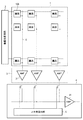
図1は、本実施形態に係る撮像装置の一例を示したブロック図である。本実施形態の撮像装置は、複数の画素100が行列状に配列された画素アレイを有する撮像領域1と、垂直走査回路2と、列増幅部3と、水平転送部4とを有する。垂直走査回路2は、画素100のトランジスタをオン(導通状態)又はオフ(非導通状態)に制御するための制御信号を供給する。撮像領域1は、画素100からの信号を列ごとに読み出すための垂直信号線6を有する。列増幅部3は、各列の画素100からの信号を増幅する、各列の垂直信号線6に接続された増幅回路31を有する。水平転送部4は、各列の増幅器に接続されたスイッチと、該スイッチをオン又はオフに制御するための制御信号を供給する水平走査回路5と、各列の増幅回路31から出力される信号を増幅する増幅回路41を有する。増幅回路41から出力される信号は、撮像装置の外部の出力信号処理部(不図示)に入力され、アナログ/デジタル変換、入力データの補正などの処理が行われる。
(First embodiment)
FIG. 1 is a block diagram illustrating an example of an imaging apparatus according to the present embodiment. The imaging apparatus of the present embodiment includes an
なお、本明細書では入出力電圧等の絶対値の比率が1以下の場合においてもこの比率を「利得」と表現する。また、利得が1以下の処理も「増幅」に含まれるものとする。すなわち、一般的には「バッファリング」(利得が約1)又は「減衰」(利得が1未満)と呼ばれるものも「増幅」に含まれる。 In this specification, even when the ratio of absolute values of input / output voltages and the like is 1 or less, this ratio is expressed as “gain”. In addition, processing with a gain of 1 or less is included in “amplification”. That is, what is generally called “buffering” (gain is about 1) or “attenuation” (gain is less than 1) is also included in “amplification”.
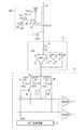
図2は、本実施形態の画素100、列増幅部3及び水平転送部4の構成をより詳細に示した図である。図1に示したように、画素領域1、列増幅部3及び水平転送部4は多数の素子により構成されているが、図2においては簡略化のため、画素100は1素子のみ、列増幅部3及び水平転送部4は1列分のみが図示されている。
FIG. 2 is a diagram showing in more detail the configuration of the
画素100は、光電変換部19及びトランジスタ20、21、22、23を有する。光電変換部19は、入射光に基づく電荷を蓄積するフォトダイオード等の光電変換素子である。各トランジスタはMOSFET(Metal-Oxide-Semiconductor Field Effect Transistor)等により構成される。本実施形態では、各トランジスタはNチャネル型のMOSFETであるものとする。
The
垂直走査回路2は、トランジスタ20、22、23のゲートに対し、それぞれ信号PTX、PSEL、PRESを供給して、撮像領域1の画素100を行ごとに制御する。トランジスタ20は、光電変換部19とトランジスタ21のゲートとの間に接続されている。信号PTXが、LowレベルからHighレベル(以下、これらをLレベル、Hレベルと表記する。)になると、光電変換部19に蓄積された電荷は、トランジスタ21のゲートである浮遊拡散部FDに転送され、保持される。トランジスタ21のドレインには電源電圧VDDが供給される。トランジスタ21のソースはトランジスタ22のドレインに接続され、トランジスタ22のソースは垂直信号線6に接続される。以上より、トランジスタ21は光電変換部19から転送された電荷に応じた電圧を垂直信号線6に出力させるソースフォロワとして機能する。電流源7は、画素100から出力される信号を読み出すためのバイアス電流を垂直信号線6に供給する。垂直走査回路2から入力される信号PSELがHレベルとなり、トランジスタ22がオンになると、トランジスタ21が出力する信号は垂直信号線6に出力される。このように、光電変換部19から転送された電荷に基づいて出力される信号を画像信号と呼ぶ。
The
トランジスタ23のソースは、トランジスタ21のゲートに接続され、トランジスタ23のドレインには、電源電圧VDDが供給されている。垂直走査回路2から入力される信号PRESがHレベルになると、トランジスタ21のゲートの浮遊拡散部FDの電位が電源電圧VDDに基づく電圧にリセットされる。浮遊拡散部FDの電位がリセットされると、リセット電位に基づく信号が垂直信号線6に出力される。このように、リセット時に浮遊拡散部FDのリセット電位に基づいて出力される信号をリセット信号(N信号)と呼ぶ。
The source of the
列増幅部3は、垂直信号線6から入力される信号を増幅して、水平転送部4に出力する回路である。列増幅部3は、スイッチ8、9、10、11、列増幅器12及び容量素子C0、C1、C2を有する。不図示のタイミングジェネレータは、スイッチ8に信号PLを、スイッチ9に信号φC1を、スイッチ10に信号φC2を、スイッチ11に信号φCを供給し、オン又はオフに制御する。なお、以下の説明において、各スイッチは、入力される信号がHレベルのときにオンになり、Lレベルのときにオフになるものとする。また、本明細書において、「スイッチ」は外部から入力される信号に基づいてオン又はオフの切り替えを行う装置を意味するものとし、例えばトランジスタにより構成することができる。以下、各スイッチもNチャネル型のMOSFETであるものとする。
The
列増幅器12は、例えばオペアンプなどの差動増幅器により構成される。以下、列増幅器12は非反転入力端子、反転入力端子及び出力端子を有する差動増幅器であるものとして説明する。垂直信号線6から入力される信号はスイッチ8及び容量素子C0を介して列増幅器12の反転入力端子に入力される。列増幅器12の反転入力端子と出力端子の間にはスイッチ9、10、11及び容量素子C1、C2を含む帰還回路が接続されている。スイッチ9の一端は列増幅器12の反転入力端子に接続され、他端は容量素子C1の一端に接続されている。容量素子C1の他端は列増幅器12の出力端子に接続されている。同様に、スイッチ10の一端は列増幅器12の反転入力端子に接続され、他端は容量素子C2の一端に接続されている。容量素子C2の他端は列増幅器12の出力端子に接続されている。スイッチ11は列増幅器12の反転入力端子と出力端子の間に接続されている。列増幅器12の非反転入力端子には基準電圧VREFが入力される。
The
列増幅部3の利得は、容量素子C0と容量素子C1の容量比(C0/C1)、又は容量素子C0と容量素子C2の容量比(C0/C2)に基づいて設定される。本実施形態では、例えば利得G1を4倍、利得G2を1倍とすることができるが、これに限定されない。利得G1と利得G2の選択は、スイッチ9とスイッチ10のいずれかをオンにして、容量素子C1と容量素子C2のいずれかを帰還容量として選択することにより行われる。
The gain of the
スイッチ11は、列増幅器12をリセットする際に列増幅器12の反転入力端子と出力端子の間及び容量素子C1、C2の両端を導通状態とするためのものである。容量素子C0、列増幅器12、スイッチ11等は第1のCDS(Correlated Double Sampling;相関二重サンプリング)回路として機能する。
The
水平転送部4は、スイッチ13、14、15、容量素子CTN、CTS1、CTS2、スイッチ16、17、18、水平走査回路5及び出力増幅器Damp1、Damp2を有する。不図示のタイミングジェネレータは、スイッチ13に信号φCTNを、スイッチ14に信号φCTS1を、スイッチ15に信号φCTS2を供給し、オン又はオフに制御する。スイッチ13、14、15の一端はそれぞれ列増幅器12の出力端子と接続され、他端は容量素子CTN、CTS1、CTS2の一端とそれぞれ接続される。容量素子CTN、CTS1、CTS2の他端は電位VSSとする。電位VSSは、例えばウェルに接続することによって与えられる。以上より、各スイッチと各容量素子は入力されたリセット信号、画像信号等の入力信号電圧を一時的に保持する保持回路を構成している。すなわち、スイッチ13、14、15を導通状態にすることで、容量素子CNT、CTS1、CTS2に列増幅器12から出力された信号をサンプルホールドすることができる。容量素子CTNには拡散浮遊部FDのリセット電位に基づくリセット信号が保持される。また、容量素子CTS1及び容量素子CTS2には、入射光の光量に基づく画像信号が保持される。
The horizontal transfer unit 4 includes
スイッチ16、17、18の一端は、スイッチ13、14、15の列増幅器12の出力端子と接続されている側の端子にそれぞれ接続される。水平走査回路5は、列増幅器12が設けられた列ごとに、スイッチ16、17、18に信号φHnを供給し、オン又はオフに制御する。水平走査回路5は、列ごとに順次スイッチ16、17、18をオンにすることにより水平走査を行う。
One ends of the
水平走査回路5がスイッチ16、17、18を導通状態とすると、容量素子CTN、CTS1、CTS2に保持された信号が、出力増幅器Damp1、Damp2に入力される。出力増幅器Damp1、Damp2も、列増幅器12と同様に、非反転入力端子、反転入力端子及び出力端子を有する差動増幅器であるものとする。スイッチ17は出力増幅器Damp1の非反転入力端子と接続され、スイッチ18は出力増幅器Damp2の非反転入力端子と接続される。スイッチ16は出力増幅器Damp1、Damp2の両方の反転入力端子に接続される。出力増幅器Damp1、出力増幅器Damp2は撮像装置に接続される不図示の出力信号処理部に信号を出力する。出力増幅器Damp1は、容量素子CTS1に保持された信号と容量素子CTNに保持された信号との差分を出力し、出力増幅器Damp2は、容量素子CTS2に保持された信号と容量素子CTNに保持された信号との差分を出力する。容量素子CTN、CTS1、CTS2と出力増幅器Damp1、Damp2とを含む回路は第2のCDS回路として機能する。第2のCDS回路によって増幅部3の利得の変化に起因するオフセット電圧が低減される。
When the
図3は、図1及び図2に示した撮像装置における、1つの画素から信号の読み出しを行う、一読み出し期間の動作を示すタイミング図である。以下、図1及び図2を参照しながら、図3のタイミング図を用いて本実施形態の撮像装置の動作について説明する。 FIG. 3 is a timing diagram illustrating an operation in one readout period in which a signal is read out from one pixel in the imaging device illustrated in FIGS. 1 and 2. Hereinafter, the operation of the imaging apparatus according to the present embodiment will be described with reference to FIGS. 1 and 2 and the timing chart of FIG.
時刻t0において、垂直走査回路2から出力される信号PTXはLレベルである。すなわち、トランジスタ20はオフであり、光電変換部19と浮遊拡散部FDとの間は電気的に非接続である。
At time t0, the signal PTX output from the
また、垂直走査回路2から出力される信号PRESはHレベルとなる。これにより、画素100の各々の浮遊拡散部FDの電位がリセットされる。さらに、垂直走査回路2から出力される信号PSELはHレベルとなる。これにより、トランジスタ21は、リセットされている浮遊拡散部FDの電位に基づく信号を、トランジスタ22を介して垂直信号線6に出力する。
Further, the signal PRES output from the
また、時刻t0において、不図示のタイミングジェネレータから出力される信号PLはHレベルとなる。これによりスイッチ8が導通状態となり、垂直信号線6の電圧が、容量素子C0を介して列増幅器12に入力される。
At time t0, signal PL output from a timing generator (not shown) becomes H level. As a result, the
また、信号φC、信号φC1、信号φC2もHレベルとなる。これにより、列増幅器12の反転入力端子と出力端子が接続されてボルテージフォロワ状態となる。また、容量素子C1、C2の両端が同電位となって、容量素子C1、C2に蓄積された電荷がリセットされる。
Further, the signal φC, the signal φC1, and the signal φC2 are also at the H level. As a result, the inverting input terminal and the output terminal of the
さらに、信号φCTN、信号φCTS1、φCTS2はHレベルとなる。これにより、水平転送部4の容量素子CTN、CTS1、CTS2は列増幅器12の出力電位を基準とした電位でリセットされる。
Further, signal φCTN, signals φCTS1, and φCTS2 are at the H level. As a result, the capacitive elements CTN, CTS1, and CTS2 of the horizontal transfer unit 4 are reset with a potential based on the output potential of the
次に、時刻t1において、不図示のタイミングジェネレータから出力される信号φC2がLレベルになり、容量素子C2は列増幅器12の反転入力端子と非接続になる。すなわち、帰還容量として容量素子C1が選択され、列増幅器12の利得はG1となる。
Next, at time t1, a signal φC2 output from a timing generator (not shown) becomes L level, and the capacitive element C2 is disconnected from the inverting input terminal of the
また、信号φCTN、信号φCTS1、信号φCTS2もLレベルとなる。これにより、容量素子CTN、容量素子CTS1、容量素子CTS2のリセットが解除される。 Further, the signal φCTN, the signal φCTS1, and the signal φCTS2 are also at the L level. Thereby, the reset of the capacitive element CTN, the capacitive element CTS1, and the capacitive element CTS2 is released.
次に、時刻t2において、信号PRESはLレベルとなる。これにより浮遊拡散部FDの電位のリセットが解除される。この際に、浮遊拡散部FDにはリセットノイズ(kTCノイズ)が混入した電位が保持される。このリセットノイズに基づく画素100からの出力信号がリセット信号である。上述のように、列増幅器12はボルテージフォロワ状態であるため、容量素子C0にはリセット信号に対応した電位が、基準電圧VREFによりクランプされる。
Next, at time t2, the signal PRES becomes L level. Thereby, resetting of the potential of the floating diffusion portion FD is released. At this time, the floating diffusion portion FD holds a potential mixed with reset noise (kTC noise). An output signal from the
次に、時刻t3において、信号φCはLレベルとなる。これにより、リセットが解除される。 Next, at time t3, the signal φC becomes L level. Thereby, the reset is released.
時刻t4において、信号φCTNはHレベルとなり、列増幅器12から出力される、増幅されたリセット信号が、容量素子CTNに印加される。その後、時刻t5において、信号φCTNはLレベルとなり、増幅されたリセット信号が容量素子CTNにサンプルホールドされる。なお、リセット信号に含まれるリセットノイズの成分は、容量素子C0にクランプされた電圧により差し引かれて列増幅器12から出力されている。よって、容量素子CTNに保持される信号には、利得G1の場合における列増幅器12のオフセット電圧が主に含まれている。
At time t4, the signal φCTN becomes H level, and the amplified reset signal output from the
次に、時刻t6において、信号PTXがHレベルとなり、その後時刻t7において、信号PTXはLレベルとなる。これにより、トランジスタ20は、光電変換部19に蓄積された電荷を浮遊拡散部FDに転送する。トランジスタ21は、浮遊拡散部FDに転送された電荷に基づく画像信号を、トランジスタ22を介して垂直信号線6に出力する。このとき、列増幅器12から増幅され出力される画像信号は、第1のCDS回路においてリセット信号が差し引かれたものとなる。
Next, at time t6, the signal PTX becomes H level, and then at time t7, the signal PTX becomes L level. Thereby, the
次に、時刻t8において、信号φCTS1がHレベルになった後、時刻t9において、信号φCTS1はLレベルとなる。これにより、列増幅器12から出力される画像信号が、容量素子CTS1にサンプルホールドされる。
Next, after the signal φCTS1 becomes H level at time t8, the signal φCTS1 becomes L level at time t9. As a result, the image signal output from the
次に、時刻t10において、信号φC1がLレベルになった後に、時刻t11において、信号φC2がHレベルになる。これにより、列増幅器12の帰還容量が容量素子C1から容量素子C2に切り替わり、列増幅部3の利得がG2に変化する。列増幅器12に入力されている信号は変化しないので、出力される信号の違いは列増幅部3の利得がG1からG2に変化したことによるものである。
Next, after the signal φC1 becomes L level at time t10, the signal φC2 becomes H level at time t11. As a result, the feedback capacitance of the
次に、時刻t12において、信号φCTS2がHレベルになった後、時刻t13において、信号φCTS2はLレベルになる。これにより、列増幅器12が出力する光信号が利得G2で増幅された画像信号が、容量素子CTS2にサンプルホールドされる。
Next, after the signal φCTS2 becomes H level at time t12, the signal φCTS2 becomes L level at time t13. As a result, the image signal obtained by amplifying the optical signal output from the
次に、時刻t14において、信号PSELがLレベルとなり、画素100は垂直信号線6と非接続となる。また、同時刻t14において、信号PLもLレベルになり、列増幅器12と垂直信号線6も非接続となる。さらに、同時刻t14において、信号φC2もLレベルになり、列増幅器12の増幅動作が停止する。
Next, at time t <b> 14, the signal PSEL becomes L level, and the
次に、時刻t15から時刻t16の期間、水平走査回路5は、信号φHnの動作を開始し、各列のスイッチ16、17、18を順次オンにする水平走査を行う。これにより、出力増幅器Damp1は、容量素子CTN、CTS1に保持した信号の差に基づく信号を、順次外部に出力し、出力増幅器Damp2は、容量素子CTN、CTS2に保持した信号の差に基づく信号を、順次外部に出力する。出力増幅器Damp1、Damp2から出力される信号をそれぞれ信号S1、S2とする。
Next, during the period from time t15 to time t16, the
ここで、出力増幅器Damp1の出力信号S1は、第2のCDS回路にて、利得G1の場合の列増幅部3のオフセット成分が差し引かれたものとなる。一方、出力増幅器Damp2の出力信号S2には、利得G2の場合の列増幅部3のオフセット成分と、利得G1の場合の列増幅部3のオフセット成分の差分が、オフセット成分として残ることとなる。
Here, the output signal S1 of the output amplifier Damp1 is obtained by subtracting the offset component of the
上述したように本実施形態の撮像装置の駆動方法では、列増幅部3のリセットが1回行われ、リセット状態における出力信号が容量素子CTNに保持される。このとき、列増幅部3の利得は利得G1(本実施形態では4倍)となっているため、容量素子CTNに保持される信号は利得G1で増幅されたものである。その後、利得G1で増幅された画像信号と、利得G2(本実施形態では1倍)で増幅された画像信号とがそれぞれ容量素子CTS1、CTS2に保持される。そして、出力増幅器Damp1、Damp2より、容量素子CTS1、CTS2に保持された信号から容量素子CTNに保持された信号を差し引いた信号が信号S1、S2として出力される。なお、画像信号を増幅する利得の値の種類をさらに多くし、3個以上としてもよい。その場合、出力増幅器の個数を利得の値の個数に応じて増加させる。
As described above, in the driving method of the imaging apparatus of the present embodiment, the
本実施形態では列増幅部3をリセットする回数が、出力される画像信号の個数よりも少ない。これにより、リセットの回数を削減し、読み出しを高速化することができる。なお、上述の例ではリセットの回数は1回のみであったが、画像信号の個数よりも少ない範囲であれば2回以上とすることもできる。ただし、1回の場合が最も読み出しの高速化に対する効果が大きく、好ましい。
In the present embodiment, the number of times that the
本実施形態の構成では、入射光量に応じて異なる利得で増幅された複数の画像信号を用いることでダイナミックレンジの拡大が可能である。そのための信号処理方法について図4(a)、図4(b)及び図4(c)を用いて説明する。 In the configuration of the present embodiment, the dynamic range can be expanded by using a plurality of image signals amplified with different gains according to the amount of incident light. A signal processing method for this will be described with reference to FIGS. 4 (a), 4 (b), and 4 (c).
図4(b)は、入射光量に対する信号S1及び信号S2の信号電圧の大きさを示す図である。図示されているように、利得G1が利得G2より大きい場合、同じ入射光量の場合、信号S1の方が大きい出力値となる。信号S1の方が信号S2よりも少ない光量で飽和するため、検出可能な光量の上限値が小さい。しかしながら、信号S1は列増幅部3で相対的に高い増幅率で増幅しているため、信号S1に含まれるノイズ成分は画素100で発生したものが主であり、列増幅部3以降で発生したノイズの割合が少ない。これに対し、信号S2は、相対的に低い増幅率で増幅しているため、信号S2に含まれるノイズ成分は信号S1に比べ、列増幅部3以降で発生したノイズの割合が大きい。しかしながら、信号S2は検出可能な光量の上限値が大きい。以上の理由により、信号S1及び信号S2は良好な精度で検出できる入射光量の範囲が異なっているため、信号S1及び信号S2を組み合わせることでダイナミックレンジを拡張した信号を得ることができる。
FIG. 4B is a diagram illustrating the magnitudes of the signal voltages of the signal S1 and the signal S2 with respect to the incident light amount. As shown in the figure, when the gain G1 is larger than the gain G2, the signal S1 has a larger output value for the same incident light amount. Since the signal S1 is saturated with a smaller amount of light than the signal S2, the upper limit value of the detectable amount of light is small. However, since the signal S1 is amplified with a relatively high amplification factor in the
信号S1と信号S2から、ダイナミックレンジを拡張した出力信号を得る信号処理方法について、図4(a)を用いて説明する。この信号処理方法は、例えば、出力増幅器Damp1、Damp2の後段に設けられた出力信号処理部において行うことができる。上述のように、出力増幅器Damp1、Damp2から出力される信号S1、S2はアナログ信号である。この信号処理方法は、信号S1、S2に対する加算、減算、乗算等の演算を含む。上記の演算は、アナログ/デジタル変換回路によりデジタルデータに変換してから行ってもよく、アナログ信号のままで、演算回路等を用いて行ってもよい。 A signal processing method for obtaining an output signal with an extended dynamic range from the signals S1 and S2 will be described with reference to FIG. This signal processing method can be performed, for example, in an output signal processing unit provided in a subsequent stage of the output amplifiers Damp1 and Damp2. As described above, the signals S1 and S2 output from the output amplifiers Damp1 and Damp2 are analog signals. This signal processing method includes operations such as addition, subtraction, and multiplication on the signals S1 and S2. The above calculation may be performed after being converted into digital data by an analog / digital conversion circuit, or may be performed using an arithmetic circuit or the like with an analog signal as it is.
まず、出力信号処理部は、出力増幅器Damp1、Damp2から入射光量に対応する信号S1、S2を取得する。 First, the output signal processing unit acquires signals S1 and S2 corresponding to the amount of incident light from the output amplifiers Damp1 and Damp2.
上述のように、信号S1及びS2の読み出し時における列増幅部3の利得はそれぞれG1及びG2である。信号S1に利得G1と利得G2の比であるG2/G1を乗算し、信号S1’を得る(S41)。これにより、入力光量に対する出力信号の傾きを信号S1’と信号S2についてほぼ同一にすることができる。
As described above, the gain of the
上述のように、出力増幅器Damp2の出力信号S2には、利得G2の場合の列増幅部3のオフセット成分と、利得G1の場合の列増幅部3のオフセット成分との差分が、オフセット成分として残留している。そのため、信号S2からS2オフセット補正値を減算し、信号S2’を得る(S42)。これにより、オフセット成分が低減された信号S2’を得ることができる。なお、S2オフセット補正値は、利得G2のときの列増幅部3のオフセット成分と利得G1のときの列増幅部3のオフセット成分とをあらかじめ測定しておき、その差分を記憶媒体に保持しておくことにより、事前に取得されたものを用いることができる。
As described above, in the output signal S2 of the output amplifier Damp2, the difference between the offset component of the
次にこれらの2つの信号S1’と信号S2’を合成する方法について述べる。上述の演算の結果得られた信号S1’と信号S2’は傾き又はオフセットが完全に一致していない場合がある。このような場合に、入射光量の範囲によって信号S1’と信号S2’のいずれか一方を選択するような単純な方法により合成を行うと、入射光量の範囲の境目付近で信号S1’と信号S2’が不連続となり、画質の劣化原因となり得る。したがって、連続的に信号S1’と信号S2’を連続的に接続し合成する処理が必要である。 Next, a method for synthesizing these two signals S1 'and S2' will be described. In some cases, the signal S1 'and the signal S2' obtained as a result of the above calculation do not completely match in slope or offset. In such a case, if the synthesis is performed by a simple method in which one of the signal S1 ′ and the signal S2 ′ is selected according to the range of the incident light quantity, the signal S1 ′ and the signal S2 near the boundary of the incident light quantity range. 'Becomes discontinuous and may cause degradation of image quality. Therefore, it is necessary to continuously connect and combine the signals S1 'and S2'.
そのため、図4(C)に示されるように、一点で信号S1’と信号S2’を合成するのではなく、入射光量Aから入射光量Bの範囲で重み付け平均を行うことにより、信号S1’と信号S2’を連続的に合成する。すなわち、入射光量がAより小さい範囲では信号S1’を選択し(S43)、入射光量がBよりも大きい範囲では信号S2’を選択する(S44)。その間のA≦入射光量≦Bの範囲では、S1’とS2’を重み付け平均する(S45)。以上のようにして、入射光量の区間に応じて選択又は重み付け平均された信号S3が生成され、出力される(S46)。出力信号をA≦入射光量≦Bの範囲での信号S3は、入力光量をIとすると下式のようになる。
S3 = S1’×a + S2’×b
ただし
a = (B−I)/(B−A)
b = 1−a
Therefore, as shown in FIG. 4 (C), the signal S1 ′ and the signal S2 ′ are not synthesized at one point, but the weighted average is performed in the range from the incident light amount A to the incident light amount B. The signal S2 ′ is continuously synthesized. That is, the signal S1 ′ is selected when the incident light amount is smaller than A (S43), and the signal S2 ′ is selected when the incident light amount is larger than B (S44). In the range of A ≦ incident light quantity ≦ B in the meantime, S1 ′ and S2 ′ are weighted and averaged (S45). As described above, the signal S3 selected or weighted averaged according to the interval of the incident light quantity is generated and output (S46). The signal S3 when the output signal is in the range of A ≦ incident light quantity ≦ B is expressed by the following equation when the input light quantity is I.
S3 = S1 ′ × a + S2 ′ × b
However, a = (BI) / (BA)
b = 1-a
ただし、信号S1’と信号S2’の合成方法はこれに限られるものではなく、信号S1’と信号S2’が連続的に接続可能であれば他の方法を用いても良い。例えば、a及びbの係数を、事前に定められたルックアップテーブルによって設定してもよい。 However, the method of combining the signal S1 'and the signal S2' is not limited to this, and other methods may be used as long as the signal S1 'and the signal S2' can be connected continuously. For example, the coefficients a and b may be set using a predetermined lookup table.
このような処理をすることで、入力光量が小さい信号に対しては、大きな利得G1で増幅された信号S1を用いることにより、列増幅部3以降で発生するノイズが低減される。よって、画像を得るために十分な大きさのS/N比の信号が取得可能である。一方、入力光量が比較的大きい信号に対しては、比較的小さな利得G2で増幅された信号S2を用いることで、光量が大きい場合も飽和せずに信号の取得が可能となる。この場合、列増幅器3以降で発生するノイズは混入し得るが、信号強度が大きいため画像を得るために十分な大きさのS/N比の信号が得られる。このことから、広い範囲の入力光量において十分なS/N比で信号が取得可能であるため、ダイナミックレンジが拡大される。
By performing such processing, for a signal with a small input light amount, noise generated after the
本発明の第1の実施形態では、列増幅部3をリセットする回数は1回であり、異なる利得G1、G2に基づく画像信号S1、S2の個数は2個である。したがって、特許文献1の構成よりもリセットを行う回数が減少しているため、信号の読み出しに要する時間が短縮され、読み出しが高速化する。一方、上述したように、リセットを行う回数を減少させた場合であっても複数の利得G1、G2を用いることによる撮像システムのS/N比の向上とダイナミックレンジの拡大という効果を享受することができる。
In the first embodiment of the present invention, the
本実施形態においては、列増幅部3に設けられた容量素子C1及び容量素子C2のいずれか1つのみを用いて利得G1、G2が決定されているが、容量素子C1及び容量素子C2に接続されるスイッチ9、10の両方をオンにして利得を設定してもよい。このようにすることで、選択可能な利得の種類を増加させることができる。
In the present embodiment, the gains G1 and G2 are determined using only one of the capacitive element C1 and the capacitive element C2 provided in the
(第2の実施形態)
本実施形態の撮像装置について、第1の実施形態とは異なる点を中心に説明する。
(Second Embodiment)
The imaging apparatus of the present embodiment will be described focusing on differences from the first embodiment.
図5は、本実施形態の撮像装置の構成を示した図である。 FIG. 5 is a diagram illustrating a configuration of the imaging apparatus according to the present embodiment.
本実施形態では、列増幅器12として差動入力端子及び差動出力端子を備えた完全差動型の差動増幅器(以下、完全差動増幅器)を用いている。完全差動増幅器を用いることで、同相信号除去比(CMRR)及び電源電圧変動除去比(PSRR)が向上する。また、完全差動増幅器ではコモンモード電圧Vcmを入力することにより、出力コモンモード電圧を制御することもできる。
In the present embodiment, as the
第1の実施形態では、列増幅器12の非反転入力端子には基準電圧VREFが入力されていたが、本実施形態では、リファレンス画素101が接続されている。リファレンス画素101は、光電変換部19を除いては画素100と同様の構成となっている。リファレンス画素101の光電変換部19には、光電変換素子に光が入射されないように、フォトダイオード等の光電変換素子の上に金属膜などの遮光膜が設けられている。このような遮光された画素を遮光画素又はオプティカルブラック(OB)画素と呼ぶ。遮光画素からは入射光がない場合に相当する信号が出力されるので、遮光画素を基準電圧源として用いることができる。なお、光電変換部19にフォトダイオードを作成せず、その代わりに電位VSSを有するウェルに接続されるように構成してもよい。
In the first embodiment, the reference voltage VREF is input to the non-inverting input terminal of the
電源電圧VDDの変動、画素に設けられたスイッチからのスイッチングノイズなどのノイズが信号に混入した場合、画素100とリファレンス画素101の双方に対し同相のノイズとして作用する。完全差動増幅器はノイズの同相成分を低減するので、上記の要因等による同相ノイズは低減される。
When noise such as fluctuations in the power supply voltage VDD or switching noise from a switch provided in the pixel is mixed in the signal, it acts on both the
次に列増幅部3の帰還回路の構成の違いについて説明する。第1の実施形態では、列増幅器12の反転入力端子と出力端子との間に帰還回路が構成されていた。これに対し、本実施形態では、列増幅器12の反転入力端子と非反転出力端子との間及び非反転入力端子と反転出力端子との間の双方にそれぞれ同じ帰還回路が構成されている。
Next, the difference in the configuration of the feedback circuit of the
また、第1の実施形態では、帰還回路において容量素子C1、C2にそれぞれ直列にスイッチ9、10が接続されている。これに対し本実施形態では、スイッチ9は設けられておらず、スイッチ10は、容量素子C2の一端と、列増幅器12の入力端子、容量素子C0、C1の一端及びスイッチ11の一端が接続されるノードとの間に接続されている。これにより、スイッチ10をオフにした場合は帰還容量の容量値がC1になり、スイッチ10をオンにした場合は帰還容量の容量値が(C1+C2)になるように構成されている。すなわち、スイッチ10がオフのときの利得G1は容量比(C0/C1)に応じて設定され、スイッチ10がオンのときの利得G2は容量比(C0/(C1+C2))に応じて設定される。
In the first embodiment, the
本実施形態では、列増幅器12として完全差動増幅器を用いることで、回路の対称性が向上されている。そのため、各スイッチが動作した際のスイッチングノイズ等のノイズが差動回路間で対称に発生する。例えば、列増幅器3の帰還容量を制御するスイッチ10をオフにする際には、スイッチ10を構成するトランジスタのゲート下に蓄積された電荷が容量素子C0側と容量素子C2側に分かれて移動する。このとき、容量素子C2側に移った電荷は、容量素子C2に蓄積され、容量素子C2の端子間電圧を変化させる。第1の実施形態のような非対称な回路の場合、容量素子C2の端子間電圧の変化がオフセット電圧の変動、ノイズ等の原因になる場合がある。これに対し、本実施形態では完全差動増幅器を用いているため、リファレンス電圧入力側の回路と、信号入力側の回路の対称性により、上記の電荷も対称に発生する。このような同相の電圧変動によるノイズは低減されるため、本実施形態の回路では、スイッチング等によるオフセット電圧の変動、ノイズが発生しにくい。
In this embodiment, the symmetry of the circuit is improved by using a fully differential amplifier as the
なお、本実施形態では、水平転送部4の増幅回路としてシングルエンドの出力増幅器Samp1、Samp2が用いられている。 In this embodiment, single-ended output amplifiers Samp1 and Samp2 are used as the amplifier circuit of the horizontal transfer unit 4.
図6は、図5に示した撮像装置の動作を示したタイミング図である。以下、図1及び図5を参照しながら、図6のタイミング図を用いて本実施形態の撮像装置の動作について説明する。 FIG. 6 is a timing chart showing the operation of the imaging apparatus shown in FIG. Hereinafter, the operation of the imaging apparatus according to the present embodiment will be described with reference to FIGS. 1 and 5 and the timing chart of FIG.
時刻t0において、垂直走査回路2から出力される信号PTXはLレベルである。すなわち、トランジスタ20はオフであり、光電変換部19と浮遊拡散部FDとの間は電気的に非接続である。また、垂直走査回路2から出力される信号PRESはHレベルとなる。これにより、画素100の各々の浮遊拡散部FDの電位がリセットされる。さらに、垂直走査回路2から出力される信号PSELをHレベルとなる。これにより、トランジスタ21は、リセットされている浮遊拡散部FDの電位に基づく信号を、トランジスタ22を介して垂直信号線6に出力する。
At time t0, the signal PTX output from the
また、時刻t0において、不図示のタイミングジェネレータから出力される信号PLはHレベルとなる。これによりスイッチ8が導通状態となり、垂直信号線6の電圧が、容量素子C0を介して列増幅器12に入力される。
At time t0, signal PL output from a timing generator (not shown) becomes H level. As a result, the
また、信号φC、信号φC2はHレベルとなる。これにより、列増幅器12の反転入力端子と非反転出力端子が接続され、非反転入力端子と反転出力端子が接続される。また、容量素子C1、C2の両端が同電位となって、容量素子C1、C2に蓄積された電荷がリセットされる。
Signals φC and φC2 are at H level. Thereby, the inverting input terminal and the non-inverting output terminal of the
さらに、信号φCT1がHレベルとなる。これにより、水平転送部4の容量素子CT1は列増幅器12の出力電位を基準とした電位でリセットされる。
Further, signal φCT1 becomes H level. As a result, the capacitive element CT1 of the horizontal transfer unit 4 is reset with a potential based on the output potential of the
次に、時刻t1において、不図示のタイミングジェネレータから出力される信号φC2がLレベルになり、容量素子C2の電位のリセットが解除される。また、容量C1のみが列増幅器12の帰還容量として機能し、列増幅部3の利得はG1(本実施形態では16倍とする)となる。
Next, at time t1, the signal φC2 output from the timing generator (not shown) becomes L level, and the reset of the potential of the capacitive element C2 is released. Further, only the capacitor C1 functions as a feedback capacitor of the
また、信号φCT1もLレベルとなる。これにより、容量素子CT1のリセットも解除される。 The signal φCT1 is also at the L level. Thereby, the reset of the capacitive element CT1 is also released.
次に、時刻t2において、信号PRESがLレベルとなる。これにより浮遊拡散部FDの電位のリセットが解除される。この際に、浮遊拡散部FDにはリセットノイズ(kTCノイズ)が混入した電位が保持される。これにより、この浮遊拡散部FDに保持された電位に基づくリセット信号が画素100及びリファレンス画素101から出力される。
Next, at time t2, the signal PRES becomes L level. Thereby, resetting of the potential of the floating diffusion portion FD is released. At this time, the floating diffusion portion FD holds a potential mixed with reset noise (kTC noise). Thereby, a reset signal based on the potential held in the floating diffusion portion FD is output from the
次に、時刻t3において、信号φCがLレベルとなる。これにより、リセットが解除される。このとき、容量素子C0には、リセット信号に対応した電位がクランプされる。 Next, at time t3, the signal φC becomes L level. Thereby, the reset is released. At this time, a potential corresponding to the reset signal is clamped in the capacitive element C0.
時刻t4において、信号PTXがHレベルとなり、その後時刻t5において、信号PTXはLレベルとなる。これにより、トランジスタ20は、光電変換部19に蓄積された電荷を、浮遊拡散部FDに転送する。トランジスタ21は、浮遊拡散部FDに転送された電荷に基づく画像信号を、トランジスタ22を介して垂直信号線6に出力する。このとき、出力される画像信号は、容量素子C0、列増幅器12、スイッチ11等による第1のCDS回路において、リセット信号が差し引かれたものとなる。
At time t4, the signal PTX becomes H level, and at time t5, the signal PTX becomes L level. Thereby, the
次に、時刻t6において、信号φCT1がHレベルとなり、その後時刻t7において、信号φCT1はLレベルとなる。これにより、列増幅器12から出力される信号が、容量素子CT1にサンプルホールドされる。
Next, at time t6, signal φCT1 becomes H level, and at time t7, signal φCT1 becomes L level. As a result, the signal output from the
次に、時刻t8から時刻t9の期間、水平走査回路5は信号φHnの動作を開始し、各列のスイッチ16、17を順次オンにする水平走査を行う。これにより、出力増幅器Samp1、Samp2は、容量素子CT1に保持した信号に基づく信号S1を、順次外部に出力する。
Next, during the period from time t8 to time t9, the
次に、時刻t10において、信号φC2がHレベルになる。これにより、容量素子C1、C2の双方が列増幅器12の帰還容量として機能し、列増幅部3の利得はG2に変化する。本実施形態では利得G2を1倍に設定する。列増幅器12に入力されている画像信号は変化しないので、出力される信号の違いは列増幅部3の利得がG1からG2に変化したことによるものである。
Next, at time t10, the signal φC2 becomes H level. As a result, both of the capacitive elements C1 and C2 function as feedback capacitors of the
次に、時刻t11において、信号φCT1がHレベルになった後、時刻t12において、信号φCT1はLレベルになる。これにより、列増幅器12の出力する光信号が利得G2で増幅された信号S2が、容量素子CT1にサンプルホールドされる。
Next, after the signal φCT1 becomes H level at time t11, the signal φCT1 becomes L level at time t12. As a result, the signal S2 obtained by amplifying the optical signal output from the
次に、時刻t13において、信号PSELがLレベルとなり、画素100及びリファレンス画素101は、垂直信号線6と非接続となる。また、同時刻t13において、信号PLもLレベルになり、列増幅器12と垂直信号線6も非接続となる。さらに、同時刻t13において、信号φC2もLレベルとなり、列増幅器12の増幅動作が停止する。
Next, at time t <b> 13, the signal PSEL becomes L level, and the
次に、時刻t14から時刻t15の期間、水平走査回路5は、信号φHnの動作を開始し、各列のスイッチ16、17を順次オンにする水平走査を行う。これにより、出力増幅器Samp1、Samp2は、容量素子CT1に保持した信号に基づく信号S2を、順次外部に出力する。
Next, during the period from time t14 to time t15, the
なお、本実施形態では、第1の実施形態とは異なり、信号S1、S2が出力増幅器Samp1、Samp2から差動信号として出力される。すなわち、出力増幅器Samp1、Samp2の出力電圧の差が出力信号となる。 In the present embodiment, unlike the first embodiment, the signals S1 and S2 are output as differential signals from the output amplifiers Samp1 and Samp2. That is, the difference between the output voltages of the output amplifiers Samp1 and Samp2 becomes an output signal.
以上のようにして出力された信号S1及びS2から、第1の実施形態と同様の方法により、ダイナミックレンジを拡大し、S/N比を向上した出力信号を得ることができる。また、第1の実施形態と同様にリセット回数が低減されているので、信号の読み出しに要する時間が短縮され、読み出しが高速化する。 From the signals S1 and S2 output as described above, an output signal having an increased S / N ratio can be obtained by expanding the dynamic range by the same method as in the first embodiment. Further, since the number of resets is reduced as in the first embodiment, the time required for signal readout is shortened, and the readout speed is increased.
これに加えて、本実施形態では、列増幅器12として完全差動増幅器を用いているため、CMRR及びPSRRが高い撮像装置を提供することができる。また、列増幅部3の対称性が高い構成であるため、列増幅部3を構成するスイッチ及び容量素子により発生するオフセット及びノイズを低減することができる。
In addition, in this embodiment, since a fully differential amplifier is used as the
本実施形態では、帰還容量として、容量素子C1と容量素子C2の間に接続されたスイッチ10により利得を変化させているが、第1の実施形態のように各容量素子に対し個別にスイッチを設けてもよい。また、本実施形態では信号S1を出力する時刻t8から時刻t9の間の期間において、信号PSEL、PLがHレベルである。しかしながら、信号PSEL、PLの両方又は一方をLレベルとすることにより、列増幅器12と、垂直信号線6、画素100とを電気的に分離してから信号S1を出力させてもよい。
In the present embodiment, as the feedback capacitor, the gain is changed by the
(第3の実施形態)
本実施形態の撮像装置について、第2の実施形態と異なる点を中心に説明する。
(Third embodiment)
The imaging apparatus according to the present embodiment will be described focusing on differences from the second embodiment.
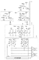
図7は、本実施形態の撮像装置の構成を示す図である。 FIG. 7 is a diagram illustrating a configuration of the imaging apparatus according to the present embodiment.
第2の実施形態では、出力増幅器Samp1、Samp2がシングルエンド入出力であるのに対し、本実施形態の出力増幅器Damp1は、差動入力、シングルエンド出力である。これにより、差動信号をシングルエンド信号に変換してから出力できるので、水平転送部4の出力線が2本から1本に減少する。 In the second embodiment, the output amplifiers Samp1 and Samp2 are single-ended input / output, whereas the output amplifier Damp1 of the present embodiment is a differential input and single-ended output. Thus, since the differential signal can be output after being converted into a single-ended signal, the number of output lines of the horizontal transfer unit 4 is reduced from two to one.
本実施形態の構成によれば、第2の実施形態と同様の効果が得られることに加えて、出力信号線の本数を少なくすることができるため、撮像装置を小型化することができる。 According to the configuration of the present embodiment, in addition to obtaining the same effects as those of the second embodiment, the number of output signal lines can be reduced, so that the imaging apparatus can be reduced in size.
(第4の実施形態)
本実施形態の撮像装置について、第2の実施形態と異なる点を中心に説明する。図8は、本実施形態の撮像装置の構成を示した図である。
(Fourth embodiment)
The imaging apparatus according to the present embodiment will be described focusing on differences from the second embodiment. FIG. 8 is a diagram illustrating a configuration of the imaging apparatus according to the present embodiment.
第2の実施形態では、容量素子CT1による保持回路が1対配置された構成であったが、本実施形態では容量素子CT1による保持回路と容量素子CT2による保持回路とがそれぞれ1対ずつ、合計2対配置されている。また、水平転送部4の増幅器として、差動入出力の出力増幅器Damp1、Damp2が、出力増幅器Samp1、Samp2の代わりに設けられている。保持容量CT1に保持された信号はスイッチ47、48を介して出力増幅器Damp1に入力され、保持容量CT2に保持された信号はスイッチ46、49を介して出力増幅器Damp2に入力される。このことにより、信号S1と信号S2を並行して水平転送部4から出力することができるため、撮像装置の動作を高速化することができる。
In the second embodiment, a pair of holding circuits by the capacitive element CT1 is arranged. However, in this embodiment, the holding circuit by the capacitive element CT1 and the holding circuit by the capacitive element CT2 each have a pair, which is a total. Two pairs are arranged. In addition, differential input / output output amplifiers Damp1 and Damp2 are provided in place of the output amplifiers Samp1 and Samp2 as amplifiers of the horizontal transfer unit 4. The signal held in the holding capacitor CT1 is input to the output amplifier Damp1 via the
図9は、図8に示した撮像装置の動作を示したタイミング図である。以下、図1及び図8を参照しながら、図9のタイミング図を用いて本実施形態の撮像装置の動作について説明する。なお、第2の実施形態と同様の動作については説明を省略する。 FIG. 9 is a timing chart showing the operation of the imaging apparatus shown in FIG. Hereinafter, the operation of the imaging apparatus of the present embodiment will be described with reference to FIGS. 1 and 8 and the timing chart of FIG. Note that description of operations similar to those of the second embodiment is omitted.
時刻t0において、第2の実施形態と同様の動作に加えて、不図示のタイミングジェネレータは、信号φCT2をHレベルとする。その後、時刻t1において、信号φCT2はLレベルとなる。この動作により、容量素子CT1と同様に容量素子CT2もリセットされる。その後時刻t7までの動作は第2の実施形態と同様である。 At time t0, in addition to the same operation as in the second embodiment, the timing generator (not shown) sets the signal φCT2 to the H level. Thereafter, at time t1, signal φCT2 becomes L level. By this operation, the capacitive element CT2 is reset as well as the capacitive element CT1. Thereafter, the operation up to time t7 is the same as in the second embodiment.
次に、時刻t8にて、信号φC2がHレベルになり、列増幅部3の利得はG1からG2に変化する。本実施形態では利得G2を1倍に設定する。
Next, at time t8, the signal φC2 becomes H level, and the gain of the
次に、時刻t9において、信号φCT2がHレベルとなり、その後、時刻t10において、信号φCT2はLレベルとなる。これにより、列増幅器12が出力する画像信号が利得G2で増幅された信号S2が、容量素子CT2にサンプルホールドされる。
Next, at time t9, the signal φCT2 becomes H level, and then at time t10, the signal φCT2 becomes L level. As a result, the signal S2 obtained by amplifying the image signal output from the
次に、時刻t11において、信号PSELがLレベルとなり、画素100及びリファレンス画素101は、垂直信号線6と非接続となる。また、同時刻t11において、信号PLもLレベルになり、列増幅器12と垂直信号線6も非接続となる。さらに、同時刻t11において、信号φC2もLレベルとなり、列増幅器12の増幅動作が停止する。
Next, at time t <b> 11, the signal PSEL becomes L level, and the
次に、時刻t12から時刻t13の期間、水平走査回路5は、信号φHnの動作を開始し、各列のスイッチ46、47、48、49を順次オンにする水平走査を行う。これにより、出力増幅器Damp1、Damp2は、容量素子CT1、CT2に保持した信号に基づく信号S1、S2を順次外部に出力する。
Next, during the period from time t12 to time t13, the
以上のようにして出力された信号S1及びS2から、第1の実施形態と同様の方法により、ダイナミックレンジを拡大し、S/N比を向上した出力信号を得ることができる。また、第1の実施形態と同様に信号の読み出しに要する時間が短縮され、読み出しが高速化する。 From the signals S1 and S2 output as described above, an output signal having an increased S / N ratio can be obtained by expanding the dynamic range by the same method as in the first embodiment. Further, as in the first embodiment, the time required for signal readout is shortened, and the readout speed is increased.
本実施形態の構成を用いることで、第2の実施形態の効果が得られることに加えて、信号S1及び信号S2を並行して外部に出力することができるため、撮像装置の動作をさらに高速化させることができる。 By using the configuration of the present embodiment, in addition to obtaining the effects of the second embodiment, the signal S1 and the signal S2 can be output to the outside in parallel. It can be made.
(第5の実施形態)
第1〜第4の実施形態で述べた撮像装置を撮像システムに適用した、第5の実施形態について述べる。撮像システムは撮像装置を用いて画像、動画等を取得する装置であり、その一例としては、デジタルスチルカメラ、デジタルカムコーダー、監視カメラなどがある。図10に、撮像システムの例としてデジタルスチルカメラに第1〜第4の実施形態の撮像装置を適用した場合のブロック図を示す。
(Fifth embodiment)
A fifth embodiment in which the imaging device described in the first to fourth embodiments is applied to an imaging system will be described. An imaging system is an apparatus that acquires an image, a moving image, and the like using an imaging apparatus, and examples thereof include a digital still camera, a digital camcorder, and a surveillance camera. FIG. 10 shows a block diagram in the case where the imaging apparatus of the first to fourth embodiments is applied to a digital still camera as an example of the imaging system.
図10において、撮像システムは被写体の光学像を撮像装置301に結像させるレンズ302、レンズ302の保護のためのバリア303及びレンズ302を通った光量を調整するための絞り304を有する。また、撮像システムは撮像装置301より出力される出力信号の処理を行う出力信号処理部305を有する。
In FIG. 10, the imaging system includes a
出力信号処理部305はデジタル信号処理部を有し、撮像装置301から出力される信号を、必要に応じて各種の補正、圧縮を行って信号を出力する動作を行う。撮像装置301から出力される信号がアナログ信号である場合、出力信号処理部305はアナログ/デジタル変換回路をデジタル信号処理部の前段に備えてもよい。デジタル信号処理部で行われる処理は、図4(a)、図4(b)及び図4(c)を用いて説明した信号処理方法を含んでもよい。また、デジタル信号処理部で行われる補正は、デジタルデータの値を定数倍して画像の輝度を変化させる補正を含んでもよく、γ補正等の画像の階調を変化させる補正を含んでもよい。
The output
また、撮像システムは、画像データを一時的に記憶する為のバッファメモリ部306、記録媒体への記録又は読み出しを行うための記憶媒体制御インターフェース(I/F)部307を有する。さらに撮像システムは、撮像データの記録又は読み出しを行うための半導体メモリ等の、着脱可能な、又は撮像システムに内蔵された、記録媒体309を有する。さらに、撮像システムは、外部のコンピュータ等と通信するための外部インターフェース(I/F)部308、各種演算とデジタルスチルカメラ全体を制御する全体制御・演算部310を有する。さらに撮像システムは、出力信号処理部305に、各種タイミング信号を出力するタイミングジェネレータ311を有する。なお、タイミング信号などの制御信号はタイミングジェネレータ311ではなく外部から入力されてもよい。すなわち、撮像システムは少なくとも撮像装置301と、撮像装置301から出力された出力信号を処理する出力信号処理部305とを有すればよい。
In addition, the imaging system includes a buffer memory unit 306 for temporarily storing image data, and a storage medium control interface (I / F)
以上のように、本実施形態の撮像システムは、第1〜第4の実施形態で述べた撮像装置301を適用して撮像動作を行うことが可能である。
As described above, the imaging system of the present embodiment can perform an imaging operation by applying the
3 列増幅部
4 水平転送部
100 画素
3 columns amplification unit 4
Claims (20)
前記複数の画素の各々を順次選択することによって、前記複数の画素の各々から順次前記リセット信号と前記画像信号とを出力させる走査回路と、
前記画素から出力された、前記トランジスタがオン状態になり、その後オフ状態になった後の前記浮遊拡散部の電位に基づく1つの画像信号を、第1の利得及び前記第1の利得とは値が異なる第2の利得を含む複数の値の利得のそれぞれで増幅することによって得られた複数の画像信号を出力する、増幅部と、
保持回路部と
を備え、
前記走査回路が、前記複数の画素のうちの第1の画素の選択を開始してから、その次に前記複数の画素のうちの第2の画素の選択を開始するまでの期間である読み出し期間において、前記保持回路部が前記増幅部から出力される前記リセット信号を保持する回数が、前記保持回路部が前記増幅部から出力された複数の増幅された画像信号を保持する回数よりも少ない
ことを特徴とする撮像装置。 Each comprising a photoelectric conversion unit for storing charge based on incident light, a floating diffusion portion, and a transistor for transferring charge accumulated in the photoelectric conversion unit to the floating diffusion region, a reset signal, images signals Output a plurality of pixels arranged in a matrix,
A scanning circuit for sequentially outputting the reset signal and the image signal from each of the plurality of pixels by sequentially selecting each of the plurality of pixels;
Output from the pixel, the transistor is turned on, and then a single image signal based on the potential of the floating diffusion portion after the off state, the first interest Toku及 beauty said first gain an amplifier unit for outputting a plurality of image signals obtained by amplifying the respective gains of the plurality of values including the values different from the second gain,
Holding circuit section ,
A readout period that is a period from when the scanning circuit starts selecting the first pixel of the plurality of pixels to when the scanning circuit starts selecting the second pixel of the plurality of pixels. in, the number of times for holding the reset signal the holding circuit is output from the amplifier unit is less than the number of times that the holding circuit holds a plurality of amplified image signal output from the amplifier unit An imaging apparatus characterized by the above.
前記複数の画素の各々を順次選択することによって、前記複数の画素の各々から順次前記リセット信号と前記画像信号とを出力させる走査回路と、
前記画素から出力された1つの画像信号を、第1の利得及び前記第1の利得とは値が異なる第2の利得を含む複数の値の利得のそれぞれで増幅することによって得られた複数の画像信号を出力する、増幅部と、
前記リセット信号と、複数の値の利得で増幅して得られた複数の画像信号との各々を保持する複数の保持回路を有する水平転送部と、
を備え、
前記走査回路が、前記複数の画素のうちの第1の画素の選択を開始してから、その次に前記複数の画素のうちの第2の画素の選択を開始するまでの期間である読み出し期間において、前記増幅部から出力される前記リセット信号の個数は、前記増幅部から出力された複数の増幅された画像信号の個数よりも少なく、
前記リセット信号を保持する保持回路の個数は、前記増幅された複数の画像信号を保持する保持回路の個数よりも少ない
ことを特徴とする撮像装置。 A plurality of pixels arranged in a matrix that outputs a reset signal that is an output signal of the reset pixel and an image signal that is an output signal based on incident light;
A scanning circuit for sequentially outputting the reset signal and the image signal from each of the plurality of pixels by sequentially selecting each of the plurality of pixels;
A plurality of image signals obtained by amplifying one image signal output from the pixel with a plurality of gain values including a first gain and a second gain having a value different from the first gain. An amplification unit for outputting an image signal;
Before Symbol reset signal, a horizontal transfer unit having a plurality of holding circuits for holding each of the plurality of image signals obtained by amplifying a gain of the plurality of values,
Bei to give a,
A readout period that is a period from when the scanning circuit starts selecting the first pixel of the plurality of pixels to when the scanning circuit starts selecting the second pixel of the plurality of pixels. The number of the reset signals output from the amplifying unit is less than the number of a plurality of amplified image signals output from the amplifying unit,
The number of holding circuits for holding a reset signal, characterized imaging device to be less than the number of the holding circuit for holding a plurality of image signals the amplification.
前記増幅部は差動入力端子と差動出力端子を有する完全差動増幅器を含み、
前記完全差動増幅器の差動入力端子のうちの第1の端子には前記リファレンス画素から出力されたリセット信号が入力され、前記完全差動増幅器の差動入力端子のうちの第2の端子には前記画素から出力された画像信号が入力される
ことを特徴とする請求項1乃至7のいずれか1項に記載の撮像装置。 The imaging device further includes a reference pixel that outputs a reset signal,
The amplifying unit includes a fully differential amplifier having a differential input terminal and a differential output terminal;
Wherein the first terminal of the differential input terminals of the fully differential amplifier is input reset signal output from the reference pixel, the second terminal of the differential input terminals of the fully differential amplifier the imaging apparatus according to any one of claims 1 to 7, characterized in that the image signal output from the pixel are input.
前記保持回路に保持された複数の画像信号は、前記水平転送部から並行して出力される
ことを特徴とする請求項10に記載の撮像装置。 The imaging apparatus further includes a horizontal transfer unit having a plurality of holding circuits that hold a plurality of image signals that are output from the differential output terminals of the fully-differential amplifier and are amplified by a plurality of gains. Prepared,
The image pickup apparatus according to claim 10 , wherein the plurality of image signals held in the holding circuit are output in parallel from the horizontal transfer unit.
前記第1の利得により増幅された画像信号に対し、前記第2の利得を前記第1の利得で除算して得た利得比を乗算し、
前記第2の利得により増幅された画像信号に対し、前記第1の利得のときのオフセット成分と、前記第2の利得のときのオフセット成分との差分を用いてオフセット成分の補正を行い、
さらに、
前記出力信号処理部は、
前記画像信号に前記利得比を乗算することにより生成された信号、
前記オフセット成分の補正により生成された信号、及び
前記乗算により生成された信号と前記オフセット成分の補正により生成された信号とを重み付け平均して得た信号
のいずれか1つを前記画素の入射光量に応じて出力する
ことを特徴とする請求項13に記載の撮像システム。 The output signal processor is
The relative first more amplified image signal to the gain of multiplying the gain ratio of the second gain obtained by dividing the first gain,
The relative more amplified image signal into a second gain, wherein the offset component when the first gain, the correction of the offset component by using the difference between the offset component when the second gain the stomach line,
further,
The output signal processor is
A signal generated by multiplying the image signal by the gain ratio ;
Signal generated by the correction of the offset component, and the pixels of one of the multiplications more generated signal and the signal obtained by weighted averaging the generated signals by the correction of the offset component It outputs according to incident light quantity. The imaging system of Claim 13 characterized by the above-mentioned.
前記複数の画素の各々を順次選択することによって、前記複数の画素の各々から順次前記リセット信号と前記画像信号とを出力させる走査回路と、
前記画素から出力された、前記浮遊拡散部の電位に基づく1つの画像信号を、第1の利得及び第2の利得を含む複数の値の利得のそれぞれで増幅することによって得られた複数の画像信号を出力する、増幅部と
を備える撮像システムの駆動方法であって、
前記走査回路が、前記複数の画素のうちの第1の画素の選択を開始してから、その次に前記複数の画素のうちの第2の画素の選択を開始するまでの期間である読み出し期間において、前記増幅部のリセットを少なくとも1回行うこと、
前記読み出し期間において、前記光電変換部に蓄積された電荷を前記浮遊拡散部に転送すること、及び
前記読み出し期間において、前記増幅部のリセット信号を保持する回数よりも、前記転送の後の前記浮遊拡散部の電位に基づく1つの画像信号を前記第1の利得及び前記第2の利得のそれぞれで前記増幅部が増幅することによって前記増幅部から出力される複数の画像信号を保持する回数を多くすること
を含むことを特徴とする方法。 Each, a photoelectric conversion unit for storing charge based on incident light, and a floating diffusion unit, a reset signal, and outputs the images signals, and a plurality of pixels arranged in a matrix,
A scanning circuit for sequentially outputting the reset signal and the image signal from each of the plurality of pixels by sequentially selecting each of the plurality of pixels;
Output from the pixels, one image signal based on the potential of the floating diffusion portion, obtained by amplifying the respective gains of the plurality of values including a first interest Toku及 beauty second gain An imaging system driving method comprising: an amplifying unit that outputs a plurality of image signals;
A readout period that is a period from when the scanning circuit starts selecting the first pixel of the plurality of pixels to when the scanning circuit starts selecting the second pixel of the plurality of pixels. in, performing at least once the reset of the amplifying unit,
Transferring the charge accumulated in the photoelectric conversion unit to the floating diffusion unit in the readout period; and
In the readout period, one image signal based on the potential of the floating diffusion unit after the transfer is obtained by each of the first gain and the second gain, rather than the number of times the reset signal of the amplification unit is held. Increasing the number of times a plurality of image signals output from the amplification unit are held by amplification by the amplification unit .
前記第2の利得により増幅された画像信号に対し、前記第1の利得のときのオフセット成分と、前記第2の利得のときのオフセット成分との差分を用いてオフセット成分の補正を行うこと、及び
前記乗算により生成された信号、前記オフセット成分の補正により生成された信号、及び前記乗算により生成された信号と前記オフセット成分の補正により生成された信号とを重み付け平均して得た信号、のいずれか1つを前記画素の入射光量に応じて出力すること
をさらに含むことを特徴とする請求項17に記載の方法。 The relative more amplified image signal to the first gain, multiplying the gain ratio of the second gain obtained by dividing the first gain,
The relative more amplified image signal into a second gain, wherein the offset component when the first gain, the correction of the offset component by using the difference between the offset component when the second gain And a weighted average of the signal generated by the multiplication, the signal generated by the correction of the offset component, and the signal generated by the multiplication and the signal generated by the correction of the offset component. The method according to claim 17 , further comprising: outputting any one of the received signals according to the amount of incident light of the pixels.
Priority Applications (3)
| Application Number | Priority Date | Filing Date | Title |
|---|---|---|---|
| JP2014165216A JP6385192B2 (en) | 2014-08-14 | 2014-08-14 | Imaging apparatus, imaging system, and driving method of imaging system |
| US14/813,485 US9894308B2 (en) | 2014-08-14 | 2015-07-30 | Imaging apparatus, imaging system, and method of driving an imaging system |
| US15/854,560 US10419702B2 (en) | 2014-08-14 | 2017-12-26 | Imaging apparatus, imaging system, and method of driving an imaging system |
Applications Claiming Priority (1)
| Application Number | Priority Date | Filing Date | Title |
|---|---|---|---|
| JP2014165216A JP6385192B2 (en) | 2014-08-14 | 2014-08-14 | Imaging apparatus, imaging system, and driving method of imaging system |
Publications (3)
| Publication Number | Publication Date |
|---|---|
| JP2016042633A JP2016042633A (en) | 2016-03-31 |
| JP2016042633A5 JP2016042633A5 (en) | 2017-09-14 |
| JP6385192B2 true JP6385192B2 (en) | 2018-09-05 |
Family
ID=55303101
Family Applications (1)
| Application Number | Title | Priority Date | Filing Date |
|---|---|---|---|
| JP2014165216A Active JP6385192B2 (en) | 2014-08-14 | 2014-08-14 | Imaging apparatus, imaging system, and driving method of imaging system |
Country Status (2)
| Country | Link |
|---|---|
| US (2) | US9894308B2 (en) |
| JP (1) | JP6385192B2 (en) |
Families Citing this family (14)
| Publication number | Priority date | Publication date | Assignee | Title |
|---|---|---|---|---|
| JP6299544B2 (en) * | 2014-09-24 | 2018-03-28 | 株式会社Jvcケンウッド | Solid-state imaging device |
| JP6628497B2 (en) | 2015-05-19 | 2020-01-08 | キヤノン株式会社 | Imaging device, imaging system, and image processing method |
| JP2018011162A (en) * | 2016-07-13 | 2018-01-18 | ソニー株式会社 | Solid-state image sensor, imaging apparatus, and control method for solid-state image sensor |
| JP6732625B2 (en) | 2016-10-07 | 2020-07-29 | キヤノン株式会社 | Imaging device and imaging system |
| JP6865589B2 (en) | 2017-01-10 | 2021-04-28 | キヤノン株式会社 | Imaging device |
| JP7297433B2 (en) | 2018-12-11 | 2023-06-26 | キヤノン株式会社 | Photoelectric conversion device and imaging system |
| JP2020108061A (en) | 2018-12-28 | 2020-07-09 | キヤノン株式会社 | Imaging device and imaging system |
| US11165978B2 (en) | 2019-04-16 | 2021-11-02 | Canon Kabushiki Kaisha | Imaging device, control method thereof, and imaging apparatus |
| JP7330739B2 (en) | 2019-04-18 | 2023-08-22 | キヤノン株式会社 | IMAGING DEVICE, IMAGING DEVICE CONTROL METHOD, COMPUTER PROGRAM, AND STORAGE MEDIUM |
| US20200334437A1 (en) * | 2019-04-22 | 2020-10-22 | Himax Technologies Limited | Optical fingerprint detecting system |
| JP7329963B2 (en) * | 2019-05-17 | 2023-08-21 | ソニーセミコンダクタソリューションズ株式会社 | Solid-state imaging device and electronic equipment |
| JP7305487B2 (en) * | 2019-08-30 | 2023-07-10 | キヤノン株式会社 | Radiation imaging apparatus, radiation imaging system, and radiation imaging apparatus control method |
| US11240458B2 (en) * | 2020-06-12 | 2022-02-01 | Omnivision Technologies, Inc. | Image sensor with capacitor randomization for column gain |
| JP2022114353A (en) | 2021-01-26 | 2022-08-05 | キヤノン株式会社 | Imaging apparatus, electronic apparatus, and image creating apparatus |
Family Cites Families (33)
| Publication number | Priority date | Publication date | Assignee | Title |
|---|---|---|---|---|
| US7002408B2 (en) * | 2003-10-15 | 2006-02-21 | Varian Medical Systems Technologies, Inc. | Data signal amplifier and processor with multiple signal gains for increased dynamic signal range |
| JP2006074497A (en) * | 2004-09-02 | 2006-03-16 | Sharp Corp | Solid-state image pickup device |
| JP4459099B2 (en) | 2005-03-18 | 2010-04-28 | キヤノン株式会社 | Solid-state imaging device and camera |
| JP4459098B2 (en) | 2005-03-18 | 2010-04-28 | キヤノン株式会社 | Solid-state imaging device and camera |
| JP4677258B2 (en) | 2005-03-18 | 2011-04-27 | キヤノン株式会社 | Solid-state imaging device and camera |
| JP4794877B2 (en) | 2005-03-18 | 2011-10-19 | キヤノン株式会社 | Solid-state imaging device and camera |
| JP4861015B2 (en) * | 2006-01-13 | 2012-01-25 | キヤノン株式会社 | Imaging device and imaging apparatus |
| JP4054839B1 (en) | 2007-03-02 | 2008-03-05 | キヤノン株式会社 | Photoelectric conversion device and imaging system using the same |
| EP2037667B1 (en) | 2007-09-14 | 2017-08-23 | Canon Kabushiki Kaisha | Image sensing apparatus and imaging system |
| JP5279352B2 (en) | 2008-06-06 | 2013-09-04 | キヤノン株式会社 | Solid-state imaging device |
| JP5188292B2 (en) * | 2008-06-30 | 2013-04-24 | キヤノン株式会社 | Imaging system and driving method of imaging system |
| JP5161676B2 (en) | 2008-07-07 | 2013-03-13 | キヤノン株式会社 | Imaging apparatus and imaging system |
| JP5404108B2 (en) | 2009-03-11 | 2014-01-29 | キヤノン株式会社 | Solid-state imaging device and driving method thereof |
| JP5235814B2 (en) | 2009-08-04 | 2013-07-10 | キヤノン株式会社 | Solid-state imaging device |
| JP5751766B2 (en) | 2010-07-07 | 2015-07-22 | キヤノン株式会社 | Solid-state imaging device and imaging system |
| JP5643555B2 (en) | 2010-07-07 | 2014-12-17 | キヤノン株式会社 | Solid-state imaging device and imaging system |
| JP5885401B2 (en) | 2010-07-07 | 2016-03-15 | キヤノン株式会社 | Solid-state imaging device and imaging system |
| JP2012034350A (en) | 2010-07-07 | 2012-02-16 | Canon Inc | Solid-state imaging device and imaging system |
| JP5645513B2 (en) | 2010-07-07 | 2014-12-24 | キヤノン株式会社 | Solid-state imaging device and imaging system |
| JP5697371B2 (en) | 2010-07-07 | 2015-04-08 | キヤノン株式会社 | Solid-state imaging device and imaging system |
| JP5656484B2 (en) | 2010-07-07 | 2015-01-21 | キヤノン株式会社 | Solid-state imaging device and imaging system |
| US8928789B2 (en) * | 2010-09-30 | 2015-01-06 | Canon Kabushiki Kaisha | Solid-state imaging apparatus |
| JP5693146B2 (en) * | 2010-10-29 | 2015-04-01 | キヤノン株式会社 | Solid-state imaging device and driving method of solid-state imaging device |
| JP6150457B2 (en) * | 2011-05-12 | 2017-06-21 | キヤノン株式会社 | Solid-state imaging device, driving method for solid-state imaging device, and solid-state imaging system |
| JP5967912B2 (en) | 2011-12-02 | 2016-08-10 | キヤノン株式会社 | Solid-state imaging device |
| JP5956755B2 (en) | 2012-01-06 | 2016-07-27 | キヤノン株式会社 | Solid-state imaging device and imaging system |
| JP5956840B2 (en) | 2012-06-20 | 2016-07-27 | キヤノン株式会社 | Solid-state imaging device and camera |
| JP5926634B2 (en) | 2012-07-03 | 2016-05-25 | キヤノン株式会社 | Solid-state imaging device and camera |
| JP6077786B2 (en) | 2012-08-22 | 2017-02-08 | キヤノン株式会社 | Imaging device |
| JP6174902B2 (en) | 2012-09-14 | 2017-08-02 | キヤノン株式会社 | Solid-state imaging device and camera |
| JP5805261B2 (en) * | 2014-04-16 | 2015-11-04 | キヤノン株式会社 | Solid-state imaging device and driving method of solid-state imaging device |
| JP6339851B2 (en) | 2014-05-01 | 2018-06-06 | キヤノン株式会社 | Solid-state imaging device and driving method thereof |
| KR101580178B1 (en) * | 2014-07-30 | 2015-12-24 | 주식회사 동부하이텍 | An image sensor including the same |
-
2014
- 2014-08-14 JP JP2014165216A patent/JP6385192B2/en active Active
-
2015
- 2015-07-30 US US14/813,485 patent/US9894308B2/en not_active Expired - Fee Related
-
2017
- 2017-12-26 US US15/854,560 patent/US10419702B2/en active Active
Also Published As
| Publication number | Publication date |
|---|---|
| US20160050381A1 (en) | 2016-02-18 |
| JP2016042633A (en) | 2016-03-31 |
| US9894308B2 (en) | 2018-02-13 |
| US20180124346A1 (en) | 2018-05-03 |
| US10419702B2 (en) | 2019-09-17 |
Similar Documents
| Publication | Publication Date | Title |
|---|---|---|
| JP6385192B2 (en) | Imaging apparatus, imaging system, and driving method of imaging system | |
| US8400546B2 (en) | Image capturing device, image capturing system, and method of driving image capturing device | |
| WO2016013412A1 (en) | Solid-state image pickup element, image pickup control method, signal processing method, and electronic apparatus | |
| JP4315032B2 (en) | Solid-state imaging device and driving method of solid-state imaging device | |
| JP2016201649A (en) | Imaging apparatus, imaging system, and driving method for imaging apparatus | |
| JP7116599B2 (en) | Imaging device, semiconductor device and camera | |
| US9762841B2 (en) | Solid state imaging device and imaging system | |
| JP2009141631A (en) | Photoelectric conversion device and image pickup device | |
| JP2009177749A (en) | Solid-state imaging apparatus | |
| US9979910B2 (en) | Image capturing apparatus and control method thereof, and storage medium | |
| JP2008301030A (en) | Solid state imaging apparatus | |
| JP6385126B2 (en) | Solid-state imaging device | |
| JP6808564B2 (en) | Signal processing devices and methods, image sensors, and image pickup devices | |
| JP2016167773A (en) | Imaging apparatus and processing method of the same | |
| JP2009130383A (en) | Image device | |
| JP2011176762A (en) | Solid-state imaging device and camera | |
| JP5222029B2 (en) | IMAGING DEVICE, IMAGING SYSTEM, AND IMAGING DEVICE CONTROL METHOD | |
| JP6896788B2 (en) | Imaging equipment, imaging methods, computer programs and storage media | |
| US10432882B2 (en) | Imaging device and endoscope system | |
| JP6422319B2 (en) | Imaging apparatus and imaging system using the same | |
| JP2019193085A (en) | Imaging device and control method of the same, and imaging apparatus | |
| JP2011035603A (en) | Solid-state imager | |
| JP4507937B2 (en) | Solid-state imaging device | |
| JP4354081B2 (en) | XY address selection type solid-state imaging device | |
| JP6555979B2 (en) | Imaging apparatus and imaging system |
Legal Events
| Date | Code | Title | Description |
|---|---|---|---|
| A521 | Request for written amendment filed |
Free format text: JAPANESE INTERMEDIATE CODE: A523 Effective date: 20170807 |
|
| A621 | Written request for application examination |
Free format text: JAPANESE INTERMEDIATE CODE: A621 Effective date: 20170807 |
|
| RD05 | Notification of revocation of power of attorney |
Free format text: JAPANESE INTERMEDIATE CODE: A7425 Effective date: 20171214 |
|
| RD04 | Notification of resignation of power of attorney |
Free format text: JAPANESE INTERMEDIATE CODE: A7424 Effective date: 20180126 |
|
| A977 | Report on retrieval |
Free format text: JAPANESE INTERMEDIATE CODE: A971007 Effective date: 20180611 |
|
| TRDD | Decision of grant or rejection written | ||
| A01 | Written decision to grant a patent or to grant a registration (utility model) |
Free format text: JAPANESE INTERMEDIATE CODE: A01 Effective date: 20180710 |
|
| A61 | First payment of annual fees (during grant procedure) |
Free format text: JAPANESE INTERMEDIATE CODE: A61 Effective date: 20180807 |
|
| R151 | Written notification of patent or utility model registration |
Ref document number: 6385192 Country of ref document: JP Free format text: JAPANESE INTERMEDIATE CODE: R151 |