JP6628497B2 - Imaging device, imaging system, and image processing method - Google Patents
Imaging device, imaging system, and image processing method Download PDFInfo
- Publication number
- JP6628497B2 JP6628497B2 JP2015101706A JP2015101706A JP6628497B2 JP 6628497 B2 JP6628497 B2 JP 6628497B2 JP 2015101706 A JP2015101706 A JP 2015101706A JP 2015101706 A JP2015101706 A JP 2015101706A JP 6628497 B2 JP6628497 B2 JP 6628497B2
- Authority
- JP
- Japan
- Prior art keywords
- pixel
- signal
- frame
- pixels
- processing unit
- Prior art date
- Legal status (The legal status is an assumption and is not a legal conclusion. Google has not performed a legal analysis and makes no representation as to the accuracy of the status listed.)
- Active
Links
Images


Classifications
-
- H—ELECTRICITY
- H04—ELECTRIC COMMUNICATION TECHNIQUE
- H04N—PICTORIAL COMMUNICATION, e.g. TELEVISION
- H04N25/00—Circuitry of solid-state image sensors [SSIS]; Control thereof
- H04N25/60—Noise processing, e.g. detecting, correcting, reducing or removing noise
- H04N25/62—Detection or reduction of noise due to excess charges produced by the exposure, e.g. smear, blooming, ghost image, crosstalk or leakage between pixels
- H04N25/626—Reduction of noise due to residual charges remaining after image readout, e.g. to remove ghost images or afterimages
-
- H—ELECTRICITY
- H04—ELECTRIC COMMUNICATION TECHNIQUE
- H04N—PICTORIAL COMMUNICATION, e.g. TELEVISION
- H04N23/00—Cameras or camera modules comprising electronic image sensors; Control thereof
- H04N23/80—Camera processing pipelines; Components thereof
-
- H—ELECTRICITY
- H04—ELECTRIC COMMUNICATION TECHNIQUE
- H04N—PICTORIAL COMMUNICATION, e.g. TELEVISION
- H04N23/00—Cameras or camera modules comprising electronic image sensors; Control thereof
- H04N23/80—Camera processing pipelines; Components thereof
- H04N23/84—Camera processing pipelines; Components thereof for processing colour signals
- H04N23/843—Demosaicing, e.g. interpolating colour pixel values
-
- H—ELECTRICITY
- H04—ELECTRIC COMMUNICATION TECHNIQUE
- H04N—PICTORIAL COMMUNICATION, e.g. TELEVISION
- H04N25/00—Circuitry of solid-state image sensors [SSIS]; Control thereof
- H04N25/10—Circuitry of solid-state image sensors [SSIS]; Control thereof for transforming different wavelengths into image signals
- H04N25/11—Arrangement of colour filter arrays [CFA]; Filter mosaics
- H04N25/13—Arrangement of colour filter arrays [CFA]; Filter mosaics characterised by the spectral characteristics of the filter elements
- H04N25/133—Arrangement of colour filter arrays [CFA]; Filter mosaics characterised by the spectral characteristics of the filter elements including elements passing panchromatic light, e.g. filters passing white light
-
- H—ELECTRICITY
- H04—ELECTRIC COMMUNICATION TECHNIQUE
- H04N—PICTORIAL COMMUNICATION, e.g. TELEVISION
- H04N25/00—Circuitry of solid-state image sensors [SSIS]; Control thereof
- H04N25/10—Circuitry of solid-state image sensors [SSIS]; Control thereof for transforming different wavelengths into image signals
- H04N25/11—Arrangement of colour filter arrays [CFA]; Filter mosaics
- H04N25/13—Arrangement of colour filter arrays [CFA]; Filter mosaics characterised by the spectral characteristics of the filter elements
- H04N25/135—Arrangement of colour filter arrays [CFA]; Filter mosaics characterised by the spectral characteristics of the filter elements based on four or more different wavelength filter elements
-
- H—ELECTRICITY
- H04—ELECTRIC COMMUNICATION TECHNIQUE
- H04N—PICTORIAL COMMUNICATION, e.g. TELEVISION
- H04N25/00—Circuitry of solid-state image sensors [SSIS]; Control thereof
- H04N25/70—SSIS architectures; Circuits associated therewith
-
- H—ELECTRICITY
- H04—ELECTRIC COMMUNICATION TECHNIQUE
- H04N—PICTORIAL COMMUNICATION, e.g. TELEVISION
- H04N25/00—Circuitry of solid-state image sensors [SSIS]; Control thereof
- H04N25/70—SSIS architectures; Circuits associated therewith
- H04N25/71—Charge-coupled device [CCD] sensors; Charge-transfer registers specially adapted for CCD sensors
- H04N25/75—Circuitry for providing, modifying or processing image signals from the pixel array
Description
本発明は撮像装置、撮像システム、および画像処理方法に関する。 The present invention relates to an imaging device, an imaging system, and an image processing method.
単板色の固体撮像装置では、カラー画像を得るために、特定の波長成分、たとえば赤(R)、緑(G)、青(B)のそれぞれの色を透過させるカラーフィルタ(CF)が所定のパターンで配列されている。CFのパターンとして、いわゆるベイヤ配列を持つものが多く利用されている。以下、RのCFが配された画素をR画素、GのCFが配された画素をG画素、BのCFが配された画素をB画素と表記し、CFが配されていない画素をW画素(ホワイト画素、クリア画素)と表記する。さらに、R画素、G画素、B画素を纏めてRGB画素またはカラー画素と表記することがある。 In the single-chip color solid-state imaging device, in order to obtain a color image, a color filter (CF) that transmits specific wavelength components, for example, red (R), green (G), and blue (B), is predetermined. Are arranged in a pattern. As a CF pattern, a pattern having a so-called Bayer array is often used. Hereinafter, a pixel in which an R CF is arranged is referred to as an R pixel, a pixel in which a G CF is arranged is referred to as a G pixel, a pixel in which a B CF is arranged as a B pixel, and a pixel in which no CF is arranged is W pixel. It is described as a pixel (white pixel, clear pixel). Further, R pixels, G pixels, and B pixels may be collectively referred to as RGB pixels or color pixels.
固体撮像装置の感度を向上するために、輝度の情報を得やすい画素の割合を増やす構成が提案されている。その中でも、可視光域の光を広く透過するW画素を用いることで、感度が向上しS/N比の高い画像を得ることができる。特許文献1には、RGB画素、W画素の画素数の比がR:G:B:W=1:1:1:1である撮像装置が記載されている。この撮像装置は、W画素の画像から検出された動き情報、フレーム毎に加算したRGB画像、W画素に基づいて、各フレーム時刻におけるRGB画像を復元している。
In order to improve the sensitivity of the solid-state imaging device, a configuration has been proposed in which the ratio of pixels from which luminance information is easily obtained is increased. Among them, by using a W pixel that transmits light in the visible light range widely, an image with high sensitivity and a high S / N ratio can be obtained.
特許文献1は、RGB画素のフレームの加算数を増加させることにより、色ノイズの低減を図っている。しかしながら、動きの大きな被写体において、色残像が生じるという問題があった。
本発明の撮像装置は、撮像素子と、信号処理部とを備える撮像装置であって、前記撮像素子は、画素信号を各々が出力する複数の画素を各々が備える第1の画素群と第2の画素群とを有し、前記第2の画素群の複数の第2の画素が出力する第2の画素信号が含む解像度情報は前記第1の画素群の複数の第1の画素が出力する第1の画素信号が含む解像度情報よりも少なく、前記信号処理部は、前記第2の画素から出力された第2の画素信号をフレーム間処理によって重み付け加算するとともに、同一の前記第1の画素から出力される複数のフレームの前記第1の画素信号のフレーム間の差分に基づいて前記重み付け加算における各フレームの重み付けを変更する。
An imaging device according to an aspect of the invention includes an imaging device and a signal processing unit, wherein the imaging device includes a first pixel group including a plurality of pixels each outputting a pixel signal, and a second pixel group. and a pixel group, the second resolution information containing the second pixel signals to the plurality of second pixels of the pixel group is output to output a plurality of first pixel of the first pixel group less than the resolution information stored in the first pixel signal comprises the signal processing unit, the second pixel signal outputted et al or the second pixel with weighted addition by inter-frame processing, the same first The weighting of each frame in the weighting addition is changed based on a difference between frames of the first pixel signal of a plurality of frames output from pixels .
本発明の画像処理方法は、撮像素子と、信号処理部とを備える撮像装置が出力する画素信号を処理する画像処理方法であって、前記撮像素子は、前記画素信号を各々が出力する複数の画素を各々が備える第1の画素群と第2の画素群とを有し、前記第2の画素群の複数の第2の画素が出力する第2の画素信号が含む解像度情報は前記第1の画素群の複数の第1の画素が出力する第1の画素信号が含む解像度情報よりも少なく、前記画像処理方法は、前記第2の画素から出力された第2の画素信号をフレーム間処理によって重み付け加算するとともに、同一の前記第1の画素から出力される複数のフレームの前記第1の画素信号のフレーム間の差分に基づいて前記重み付け加算における各フレームの重み付けを変更する。 An image processing method of the present invention is an image processing method for processing a pixel signal output by an imaging device including an image sensor and a signal processing unit, wherein the image sensor includes a plurality of image sensors each of which outputs the pixel signal. It has a first pixel group and a second pixel group each including a pixel, and the resolution information included in the second pixel signal output from the plurality of second pixels of the second pixel group is the first pixel group. first less than the resolution information including pixel signals to the first pixel is output pixel group of the plurality, the image processing method between the second and the second pixel signal frame output pixel or al In addition to performing weighted addition by processing, the weighting of each frame in the weighted addition is changed based on a difference between frames of the first pixel signal of a plurality of frames output from the same first pixel .
本発明によれば、動画像における色ノイズを低減しながら、動きの大きな被写体において色残像を抑制し、動画像の高画質化を図ることができる。 ADVANTAGE OF THE INVENTION According to this invention, while reducing the color noise in a moving image, the afterimage of a moving subject can be suppressed, and the image quality of a moving image can be improved.
以下、図面を参照しながら各実施形態の撮像装置について説明する。 Hereinafter, the imaging device of each embodiment will be described with reference to the drawings.
(第1の実施形態)
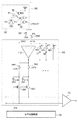
図1は、本発明の第1の特徴である画像処理のブロック図である。撮像装置は、撮像素子1と信号処理部2を備える。撮像素子1は、CMOSイメージセンサ、またはCCDイメージセンサ上にカラーフィルタが配置された、いわゆる単板式のカラーセンサである。単板のカラーセンサでカラー画像を形成する際には、後述するように補間を行う必要がある。たとえば、R画素の部分にはG、Bの情報(画素値)がない。このため、R画素の周囲のG、Bの画素値に基づき、R画素の部分におけるG、Bの画素値が補間処理により生成される。撮像素子1は、行列状に配置された複数の画素を備え、例えば列方向に1920画素、行方向に1080画素の合計2073600画素を備える。撮像素子1の画素数は限定されず、より多い画素数、若しくはより少ない画素数でも良い。さらに、撮像装置は、必ずしも撮像素子1を備えなくても良く、撮像素子1からの画素信号(RAWデータ)を処理する信号処理部2を備えていれば良い。
(1st Embodiment)
FIG. 1 is a block diagram of image processing which is the first feature of the present invention. The imaging device includes an
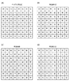
本実施形態のCFは、図1に示されたRGBW12配列を用いている。RGBW12配列においては、4×4の画素配列が繰り返されており、各色の画素数の比は、R:G:B:W=1:2:1:12である。RGBW12配列においては、カラー画素であるR、G、Bの各画素が8個のW画素で囲まれており、W画素の比率が全画素の3/4を占めている。換言すると、RGBW12配列は、第1の画素群としてW画素を有し、第2の画素群としてカラー画素(RGB画素)を有している。第1の画素群の画素数の総和は第2の画素群の画素数の総和の3倍以上(2倍より多い)であり、第2の画素群の解像度情報は第1の画素群の解像度情報よりも少ない。なお、撮像素子1には、有効な画素以外に、オプティカルブラック画素、光電変換部を有さないダミー画素などのように画像を出力しない画素が含まれ得る。但し、これらのオプティカルブラック画素、ダミー画素は第1の画素群、第2の画素群には含まれない。W画素はRGB画素と比べて広い分光感度特性および高い感度を有している。たとえば、W画素の分光感度特性の波長半値幅はRGB画素と比べて高い。
The CF of the present embodiment uses the RGBW12 array shown in FIG. In the RGBW12 array, a 4 × 4 pixel array is repeated, and the ratio of the number of pixels of each color is R: G: B: W = 1: 2: 1: 12. In the RGBW12 array, each of the R, G, and B color pixels is surrounded by eight W pixels, and the ratio of W pixels occupies 3/4 of all pixels. In other words, the RGBW12 array has W pixels as the first pixel group, and has color pixels (RGB pixels) as the second pixel group. The total number of pixels of the first pixel group is at least three times (more than twice) the total number of pixels of the second pixel group, and the resolution information of the second pixel group is the resolution of the first pixel group. Less than information. Note that the
RGBW12配列においては、RGB画素のそれぞれの周囲にはW画素が配されているため、RGB画素におけるWの画素値を高精度に補間することができる。また、W画素が全画素の3/4を占めているため、感度を向上させることができる。本実施形態は、解像度情報を得るための画素が半数以上を占める撮像素子に特に有効である。 In the RGBW12 array, W pixels are arranged around each of the RGB pixels, so that the pixel value of W in the RGB pixels can be interpolated with high accuracy. Further, since the W pixels occupy 3/4 of all the pixels, the sensitivity can be improved. The present embodiment is particularly effective for an image sensor in which pixels for obtaining resolution information occupy more than half.
信号処理部2は、前段処理部203、輝度信号処理部204、制御部205、色信号処理部206、信号合成部207を備える。撮像素子1からの画素信号は前段処理部203に入力される。前段処理部203は画素信号のオフセット補正、ゲイン補正を含む様々な補正を実行する。撮像素子1から出力された画素信号がアナログ信号である場合には、A/D変換を前段処理部203で実施してもよい。
The
前段処理部203は、入力された画素信号Dinのオフセット(OFFSET)補正、ゲイン(GAIN)補正、等の補正を適宜実施して、補正後の出力Doutを作成する。この処理は、典型的には以下の式で表わされる。
![]()
![]()
この補正は様々な回路単位で行い得る。例えば、画素毎に補正を行ってもよく、さらには、列増幅器毎、アナログデジタル変換部(ADC)、出力増幅器のそれぞれの回路毎に補正を行ってもよい。補正を行うことで、いわゆる固定パターンノイズが低減され、より高品質な画像を得ることができる。前段処理部203は、解像度情報ためのWの画像信号(輝度信号)と色情報のためのRGBの画素信号(色信号)を分離し、輝度信号を輝度信号処理部204に出力し、色信号を色信号処理部206に出力する。
This correction can be made in various circuit units. For example, the correction may be performed for each pixel, or may be performed for each circuit of a column amplifier, an analog-to-digital converter (ADC), and an output amplifier. By performing the correction, so-called fixed pattern noise is reduced, and a higher quality image can be obtained. The pre-processing unit 203 separates a W image signal (luminance signal) for resolution information from an RGB pixel signal (color signal) for color information, and outputs a luminance signal to the luminance
輝度信号処理部204は前段処理部203からの信号を高精度に補間することができる。すなわち、RGBW12配列においては、解像度情報を得るためのW画素が多いため、市松模様のCF配列に対し、空間周波数の高い、すなわちピッチの細かい情報を得ることができる。よって、RGB画素が存在する部分、つまりW画素が存在しない部分の画素値を、近傍8個のW画素の画素値の平均から求めることで、十分に高解像度の画像を得ることができる。さらに、エッジ情報、周期的な形状などの情報をもとに、エッジを検出し、RGB画素の位置におけるW画素の補間を行ってもよい。この場合、近傍8画素からの平均を用いるよりも高解像度の画像を得ることが可能となる。以下、補間により生成されたW画素をiWと表記する。
The luminance
色信号処理部206は色信号であるRGBの画素信号に対してフレーム間処理を行うことにより、偽色などの色ノイズを低減する。フレーム間処理は、時刻の異なる複数のフレームを重み付け加算することにより行われる。また、色信号処理部206は輝度信号と色信号との合成に用いられる色情報を生成する。制御部205は輝度信号のフレーム間の変化(相関)を判断し、判断結果に基づき色信号処理部206におけるフレーム間処理のフレーム数(重み付け)を変更する。これにより、動きの大きな被写体における色残像などの色ノイズを抑制することができる。
The color
図2は本実施形態に係る撮像素子1のブロック図である。撮像素子1は、撮像領域101、垂直走査回路102、列増幅部103、水平走査回路104、出力部105を有する。撮像領域101は上述したように画素100が行列状に配されており、輝度信号のための第1の画素群、色信号のための第2の画素群を備える。垂直走査回路102は、画素100のトランジスタをオン(導通状態)またはオフ(非導通状態)に制御するための制御信号を供給する。垂直信号線106は、画素100の各列に設けられ、画素100からの信号を列ごとに読み出す。水平走査回路104は、各列の増幅器に接続されたスイッチと、該スイッチをオンまたはオフに制御するための制御信号を供給する。出力部105はバッファアンプ、差動増幅器などから構成され、列増幅部103からの画素信号を撮像素子1の外部の信号処理部2に出力する。出力された画素信号は信号処理部2によって、アナログ/デジタル変換、入力データの補正などの処理が行われる。
FIG. 2 is a block diagram of the
なお、撮像素子1はアナログ/デジタル変換の機能を備えたいわゆるデジタルセンサであっても良い。画素100には、分光感度特性を制御するためのCFが設けられており、本実施形態においてはRGBW12のCFが配置されている。
Note that the
図3は本実施形態に係る撮像素子1の画素100、列増幅部103の回路図である。ここでは、説明を容易にするため、列増幅部103のうちの1列分の回路と、1つの画素100とが示されている。画素100はフォトダイオードPD、浮遊拡散容量FD、転送トランジスタM1、リセットトランジスタM2、増幅トランジスタM3、選択トランジスタM4を備える。なお、画素100は、複数のフォトダイオードPDが浮遊拡散容量FD、リセットトランジスタM2、増幅トランジスタM3、選択トランジスタM4を共有する構成を備えていても良い。また、トランジスタM2〜M4はNチャネルMOSに限定されず、PチャネルMOSによって構成されても良い。
FIG. 3 is a circuit diagram of the
フォトダイオードPDは照射された光を電子(電荷)に光電変換する。転送トランジスタM1のゲートには信号TXが供給され、信号TXがハイレベルになると、転送トランジスタM1はフォトダイオードPDに発生した電荷を浮遊拡散容量FDに転送する。浮遊拡散容量FDは、転送トランジスタM1のドレイン端子を兼ねており、転送トランジスタM1を介してフォトダイオードPDから転送される電荷を保持可能である。リセットトランジスタM2のゲートには信号RESが供給され、信号RESがハイレベルになると、リセットトランジスタM2は浮遊拡散容量FDの電圧をリセット電圧VDDにリセットする。転送トランジスタM1とリセットトランジスタM2を同時にオンにさせることにより、フォトダイオードPDの電子がリセットされる。増幅トランジスタM3のゲートは、浮遊拡散容量FDに接続される。 The photodiode PD photoelectrically converts the irradiated light into electrons (charges). The signal TX is supplied to the gate of the transfer transistor M1, and when the signal TX becomes high level, the transfer transistor M1 transfers the charge generated in the photodiode PD to the floating diffusion capacitance FD. The floating diffusion capacitance FD also serves as the drain terminal of the transfer transistor M1, and can hold the charge transferred from the photodiode PD via the transfer transistor M1. The signal RES is supplied to the gate of the reset transistor M2, and when the signal RES becomes high level, the reset transistor M2 resets the voltage of the floating diffusion capacitance FD to the reset voltage VDD. By turning on the transfer transistor M1 and the reset transistor M2 at the same time, the electrons of the photodiode PD are reset. The gate of the amplification transistor M3 is connected to the floating diffusion capacitance FD.
増幅トランジスタM3のソースは、選択トランジスタM4を介して列ごとに共通の垂直信号線106のノードPDOUTに電気的に接続され、ソースフォロアを構成する。選択トランジスタM4のゲートには信号SELが印加され、信号SELがハイレベルとなると、垂直信号線106と増幅トランジスタM3が電気的に接続される。これにより、選択された画素100から画素信号が読み出される。
The source of the amplification transistor M3 is electrically connected to the node PDOUT of the common
画素100に供給される信号TX、信号RES、信号SELは垂直走査回路102から出力される。垂直走査回路102はこれらの信号レベルを制御することによって、画素100を行単位で走査する。電流源107は垂直信号線106を介して画素100に電流を供給し、垂直信号線106は信号PLによって駆動されるスイッチSW0を介して列増幅部103に接続されている。
The signal TX, the signal RES, and the signal SEL supplied to the
列増幅部103は、列増幅器112、入力容量C0、帰還容量C1、C2、スイッチSW1〜SW7、容量CTN、CTSを有する。列増幅器112は反転入力ノード、非反転入力ノード、出力ノードを備える差動増幅回路から構成されている。列増幅器112の反転入力ノードはスイッチSW0、入力容量C0を介して垂直信号線106に電気的に接続され、非反転入力ノードには基準電圧VREFが印加されている。反転入力ノードと出力ノードとは並列接続された3つの帰還回路を介して互いに接続されている。第1の帰還回路は直列に接続されたスイッチSW1および帰還容量C1から構成され、第2の帰還回路は直列に接続されたスイッチSW2および帰還容量C2から構成され、第3の帰還回路はスイッチSW3から構成されている。スイッチSW1〜SW3のオン、オフを適宜制御することにより、列増幅器112の増幅率を変更することができる。すなわち、スイッチSW1のみがオンとなると、増幅率はC0/C1となり、スイッチSW2のみがオンとなると、増幅率はC0/C2となる。また、スイッチSW1、SW2がオンとなると、増幅率はC0/(C1+C2)となり、スイッチSW3のみがオンとなると、列増幅器112はボルテージフォロアとして動作する。スイッチSW1〜SW3は信号φC〜φC2によってそれぞれ制御される。
The
列増幅器112の出力ノードは、信号φCTNによって制御されるスイッチSW4を介して容量CTNに接続されている。同様に、列増幅器112の出力ノードは、信号φCTSによって制御されるスイッチSW5を介して容量CTSに接続されている。浮遊拡散容量FDのリセット時において、スイッチSW4がオン、スイッチSW5がオフとなり、リセット時の画素信号(N信号)が容量CTNにサンプルホールドされる。光電変換された電荷が浮遊拡散容量FDに転送された後、スイッチSW4がオフ、スイッチSW5がオンとなり、光電変換された電荷に基づく画素信号(S信号)が容量CTSにサンプルホールドされる。
The output node of
容量CTNはスイッチSW6を介して出力部105の第1入力ノードに接続され、容量CTSはスイッチSW7を介して出力部105の第2入力ノードに接続されている。水平走査回路104が各列の信号φHnを順にハイレベルとすることにより、水平走査が行われる。すなわち、信号φHnがハイレベルとなると、スイッチSW6は容量CTNに保持されたN信号を出力部105の第1入力ノードに出力し、スイッチSW7は容量CTSに保持されたS信号を出力部105の第2入力ノードに出力する。
The capacitance CTN is connected to a first input node of the
出力部105は差動増幅回路から構成されており、入力されたS信号、N信号の差分を増幅および出力することにより、リセット時のノイズ成分が除去された画素信号を出力する。なお、N信号、S信号をアナログ/デジタル変換した後に、相関二重サンプリングを行っても良い。
The
上述のように、撮像素子1に入力された光信号は、電気信号として読み出される。また、RGBW12のCF配列に応じた分光強度の2次元情報が得られる。本実施形態はRGBW12のCF配列に限定されることなく、様々なCF配列に適用可能である。以下、本実施形態において適用可能なCF配列の例を示す。
As described above, the optical signal input to the
図4にカラー画素としてRGBを用いたCF配列の例を示す。図4(a)はベイヤ配列のCFを示し、CFの数の比率がR:G:Bが1:2:1となっている。ここで、G画素(第1の画素)がRB画素(第2の画素)に比して多く配置されているのは、人間の視覚特性が赤色、青色に比して、緑色に対応する波長に対して高い感度を有し、画像の解像感も、赤色、青色に比して、緑色の波長に強く依存するからである。 FIG. 4 shows an example of a CF array using RGB as color pixels. FIG. 4A shows CF in the Bayer array, and the ratio of the number of CFs is 1: 2: 1 for R: G: B. Here, the reason why the number of G pixels (first pixels) is larger than that of RB pixels (second pixels) is that human visual characteristics correspond to wavelengths corresponding to green compared to red and blue. This is because the image has a high sensitivity, and the resolution of the image is more strongly dependent on the wavelength of green than in red and blue.
図4(b)はRGBW12のCF配列を示している。上述したように、この配列では、4×4の画素配列中、各CFがR:G:B:W=1:2:1:12の比で配置されている。カラー画素であるRGBの各画素(第2の画素)に対して、平面視において上下方向、左右方向、斜め方向のそれぞれにW画素(第1の画素)が隣接して配されている。すなわち、RGB画素の各々は8つのW画素に囲まれている。W画素は、全画素の3/4の比率を占めている。カラー画素であるRGB画素の各々がW画素によって囲まれている。 FIG. 4B shows a CF array of RGBW12. As described above, in this array, in the 4 × 4 pixel array, each CF is arranged in a ratio of R: G: B: W = 1: 2: 1: 12. A W pixel (first pixel) is arranged adjacent to each of the RGB pixels (second pixels), which are color pixels, in the vertical direction, the horizontal direction, and the oblique direction in plan view. That is, each of the RGB pixels is surrounded by eight W pixels. W pixels occupy 3/4 of all pixels. Each of the RGB pixels, which are color pixels, is surrounded by W pixels.
図4(c)はRGBW8のCF配列を示している。4×4の画素配列中、各CFがR:G:B:W=2:4:2:8の比で配列されている。W画素(第1の画素)は市松模様に配置されており、W画素の間にRGB画素(第2の画素)が配置されている。W画素の比率は全画素の1/2である。W画素はベイヤ配列のG画素と同様に市松模様に配置されているため、ベイヤ配列のG画素の補間の方法をそのまま用いることができる。また、W画素が配置されているため、感度を向上させることができる。 FIG. 4C shows the CF arrangement of RGBW8. In the 4 × 4 pixel array, each CF is arranged at a ratio of R: G: B: W = 2: 4: 2: 8. W pixels (first pixels) are arranged in a checkered pattern, and RGB pixels (second pixels) are arranged between the W pixels. The ratio of W pixels is 1/2 of all pixels. Since the W pixels are arranged in a checkered pattern like the G pixels in the Bayer array, the interpolation method for the G pixels in the Bayer array can be used as it is. Further, since the W pixels are arranged, the sensitivity can be improved.
図4(d)はRGBG12のCF配列を示している。この配列ではRGBW12のW画素がG画素(第1の画素)に置き換えており、4×4の画素配列中、各色のCFがR:G:B=2:12:2の比で配置されている。RB画素(第2の画素)がG画素で囲まれており、G画素の比率が全画素の3/4を占めている。RB画素がG画素で囲まれているため、カラー画素のGの値の補間の精度が向上する。また、RB画素に比較して感度の高いG画素の割合が高いため、感度を向上させることができる。 FIG. 4D shows the CF sequence of RGBG12. In this arrangement, W pixels of RGBW12 are replaced with G pixels (first pixels), and CF of each color is arranged in a ratio of R: G: B = 2: 12: 2 in a 4 × 4 pixel array. I have. RB pixels (second pixels) are surrounded by G pixels, and the ratio of G pixels occupies 3/4 of all pixels. Since the RB pixels are surrounded by the G pixels, the accuracy of interpolation of the G values of the color pixels is improved. Further, since the ratio of G pixels having high sensitivity is higher than that of RB pixels, the sensitivity can be improved.
図5に、カラー画素として補色であるC(シアン)・M(マゼンダ)・Y(イエロー)を用いているCF配列の例を示す。図5(a)はベイヤ配置であり、各色のCFの比率がC:M:Yが1:1:2になる。ここで、Y画素(第1の画素)が多く配置されているのは、G画素と同様にY画素の感度が高いからである。 FIG. 5 shows an example of a CF array using complementary colors C (cyan), M (magenta), and Y (yellow) as color pixels. FIG. 5A shows a Bayer arrangement in which the CF ratio of each color is C: M: Y of 1: 1: 2. Here, the reason why many Y pixels (first pixels) are arranged is that the sensitivity of the Y pixels is high like the G pixels.
図5(b)はCMYW12のCF配列を示している。4×4の画素配列中、各色のCFがC:M:Y:W=1:1:2:12の比で配列されている。カラー画素であるC、M、Yの画素(第2の画素)はW画素に囲まれている。W画素の比率が全画素の3/4を占める。CMY画素がW画素で囲まれているため、CMY画素の位置におけるW画素値の補間の精度を向上させることができる。また、W画素が配列されているため、感度が向上する。 FIG. 5B shows a CF array of CMYW12. In the 4 × 4 pixel array, CFs of each color are arranged at a ratio of C: M: Y: W = 1: 1: 2: 12. C, M, and Y pixels (second pixels), which are color pixels, are surrounded by W pixels. The ratio of W pixels occupies 3/4 of all pixels. Since the CMY pixels are surrounded by the W pixels, the accuracy of the interpolation of the W pixel values at the positions of the CMY pixels can be improved. Further, the sensitivity is improved because the W pixels are arranged.
図5(c)はCMYW8のCF配列を示している。4×4の画素配列中、各色のCFがC:M:Y:W=2:2:4:8の比で配列されている。W画素(第1の画素)が市松模様に配置されており、CMY画素(第2の画素)はW画素に囲まれている。W画素の比率が全画素の1/2である。W画素はベイヤ配列のG画素と同様に市松模様に配列されているため、ベイヤ配列のG画素の補間の方法をそのまま用いることができる。また、W画素が配列されていることにより、感度が向上する。 FIG. 5C shows a CF array of CMYW8. In the 4 × 4 pixel array, CFs of each color are arranged at a ratio of C: M: Y: W = 2: 2: 4: 8. W pixels (first pixels) are arranged in a checkered pattern, and CMY pixels (second pixels) are surrounded by W pixels. The ratio of W pixels is 1/2 of all pixels. Since the W pixels are arranged in a checkered pattern similarly to the G pixels in the Bayer array, the interpolation method of the G pixels in the Bayer array can be used as it is. In addition, the sensitivity is improved by arranging the W pixels.
図5(d)はCMYY12のCF配列を示している。CYMW12のW画素がY画素(第1の画素)に置き換えられており、4×4の画素配列中、各CFがC:M:Y=2:2:12の比で配置されている。C画素、M画素(第2の画素)がY画素で囲まれており、Y画素の比率が全画素の3/4を占めている。C画素、M画素がY画素で囲まれているため、C画素、M画素の位置におけるYの画素値の補間の精度を向上させることができる。また、C画素とM画素に対し比較的感度の高いY画素の割合が高いため、感度が向上する。 FIG. 5D shows a CF array of CMYY12. The W pixels of the CYMW 12 are replaced with Y pixels (first pixels), and each CF is arranged in a 4 × 4 pixel array at a ratio of C: M: Y = 2: 2: 12. C pixels and M pixels (second pixels) are surrounded by Y pixels, and the ratio of Y pixels occupies 3/4 of all pixels. Since the C pixel and the M pixel are surrounded by the Y pixel, it is possible to improve the accuracy of the interpolation of the Y pixel value at the positions of the C pixel and the M pixel. Further, since the ratio of the Y pixel having relatively high sensitivity to the C pixel and the M pixel is high, the sensitivity is improved.
上述のように、本実施形態において各種CF配列を採用し得るが、高解像度の画像を生成するためには、解像度に寄与する割合の高い画素(第1の画素)をより多く配置することが好ましい。第1の画素群は第2の画素群と比較して解像度情報を多く含むとともに、第2の画素群は分光感度の異なる2種以上の画素を備えることが望ましい。また、第1の画素群は第2の画素群と比較して輝度への寄与度が高いことが望ましい。 As described above, various CF arrays can be employed in the present embodiment, but in order to generate a high-resolution image, it is necessary to arrange more pixels (first pixels) that contribute to the resolution more. preferable. The first pixel group desirably includes more resolution information than the second pixel group, and the second pixel group preferably includes two or more types of pixels having different spectral sensitivities. Further, it is desirable that the first pixel group has a higher contribution to luminance than the second pixel group.
なお、ベイヤ配列においては、解像度に寄与するG画素が市松模様に配置されており、補間のエラーが生じ易い。発明者らは、市松模様に比べて高い解像度を作りだすCF配列を用いることで、補間エラーを極力小さくできることを見出した。従って、図4(b)のRGBW12、図4(d)のRGBG12、図5(b)のCMYW12、図5(d)のCMYY12に例示されるCF配列を用いた場合に、本発明の効果が特に顕著となる。 In the Bayer array, G pixels that contribute to the resolution are arranged in a checkered pattern, and interpolation errors are likely to occur. The inventors have found that an interpolation error can be minimized by using a CF array that produces a higher resolution than a checkerboard pattern. Therefore, the effects of the present invention can be obtained by using the CF arrays exemplified in RGBW12 in FIG. 4B, RGBG12 in FIG. 4D, CMYW12 in FIG. 5B, and CMYY12 in FIG. This is particularly noticeable.
図6は、本実施形態に係る撮像装置の信号処理部2のブロック図である。信号処理部2は輝度信号処理部204、制御部205、色信号処理部206、信号合成部207を備え、撮像素子1からの画素信号3aをデモザイク処理し、各画素がRGBの情報を有する画像信号3gを生成する。信号処理部2は画像処理プロセッサなどのハードウェアによって構成され得るが、汎用のプロセッサまたはコンピュータ上のソフトウェアを用いて同様の構成を実現することも可能である。
FIG. 6 is a block diagram of the
輝度信号処理部204には、RGBW12のCF配列を有するとともに、デジタルデータで表された画素信号3bが入力される。図6には、CF配列の繰り返しの1単位となる4×4画素が示されているが、実際の画素信号3aにおいては4×4画素の配列が繰り返されている。入力された画素信号3aは、図示されていない前段処理部203によって、Wの画素信号3bと、RGBの画素信号3eとに分離される。
The luminance
輝度信号処理部204は補間処理部211を備え、補間処理部211はWの画素信号3bにおいてWの画素値が存在しない部分の画素値を補間により生成する。Wの画素信号3bにおいてRGB画素を分離した位置にはWの画素値は存在せず、図中、この位置は”?”と表記されている。補間処理部211は”?”の位置の画素値を周囲のWの画素値に基づき補間し、iWr、iWg、iWbの画素値を補間により生成する。例えば、画素信号3bにおける座標(3,3)にはW画素が存在しないため、次式で表されるように、周囲の8個のW画素値の平均値から、座標(3,3)におけるiWb(3,3)の画素値が求められる。
![]()
![]()
なお、図6には4×4の画素配列が記載されているが、実際には画素配列が繰り返されており、座標(1,1)のR画素、座標(3,1)のG画素、座標(1,3)のG画素のそれぞれは8個のW画素に囲まれている。よって、iWr、iWgの画素値も同様に周囲の8個のWの画素値を用いて補間により生成することができる。 Although FIG. 6 shows a 4 × 4 pixel array, the pixel array is actually repeated, and an R pixel at coordinates (1, 1), a G pixel at coordinates (3, 1), Each of the G pixels at the coordinates (1, 3) is surrounded by eight W pixels. Therefore, similarly, the pixel values of iWr and iWg can be generated by interpolation using eight surrounding W pixel values.
補間処理法としては、上述した方法の他、バイリニア法、バイキュービック法等を適宜用いることができる。 As the interpolation processing method, in addition to the above-described method, a bilinear method, a bicubic method, or the like can be appropriately used.
制御部205は空間平均処理部212、判定処理部213を備える。空間平均処理部212はWの画素信号3bにおいて所定ブロック毎に画素の平均値Waveを算出する。判定処理部213は平均値Waveのフレーム間の差分と閾値とを比較し、比較結果に基づく判定信号Jを出力する。色信号処理部206はフレーム間処理部214を備え、フレーム間処理部214はRGBの画素信号3eのフレーム間処理を行い、色ノイズ、偽色を低減する。信号合成部207は、フレーム間処理されたRGBの各画素とW画素との色比情報を算出し、当該色比情報に基づきRGBの画素値で表された画像信号3gを生成する。
The
図7(a)、図7(b)は、制御部205における空間平均処理の画素領域の一例を示している。RGBW12画素配列の1ブロックは4×4画素から構成されているので、1ブロックに含まれるWの画素値の平均値を算出し得る。すなわち、図7(a)において、(x、y)=(2,1)、(4,1)、(1,2)、(2,2)、(3,2)、(4,2)、(2,3)、(4,3)、(1,4)、(2,4)、(3,4)、(4,4)の12画素のW値の空間平均を演算し、ブロック毎に平均値Waveを算出し得る。このようにして算出された平均値Waveは、同一ブロックに含まれる(x、y)=(1,1)、(3,1)、(1,3)、(3,3)のRGB画素のフレーム間処理の判定において用いられる。
FIGS. 7A and 7B show an example of a pixel area in the spatial averaging process in the
図7(b)は、空間平均処理の画素領域の他の例を示している。RGBW12画素配列において、RGB画素の各々はW画素に囲まれている。例えば、(x、y)=(3,3)のB画素は、(x、y)=(2,2)、(3,2)、(4,2)、(2,3)、(4,3)、(2,4)、(3,4)、(4,4)の8個のW画素によって囲まれている。従って、これらの8個のW画素の平均値Waveを、(3,3)のB画素のフレーム間処理の判定のために用いてもよい。同様に、(5,3)のG画素の周囲の8個のW画素の平均値Waveを、(5,3)のG画素のフレーム間処理の判定のために用いることができる。図7(a)、(b)のいずれの例においても、フレーム間処理の対象となるRGBの画素の周囲の複数のWの画素値を用いて、画素領域毎の平均値Waveが算出される。なお、単純平均に限定されず、重み付け平均、平滑化フィルタなどを用いて空間平均処理を行っても良い。 FIG. 7B shows another example of the pixel area of the spatial averaging process. In the RGBW12 pixel array, each of the RGB pixels is surrounded by W pixels. For example, B pixels of (x, y) = (3, 3) are (x, y) = (2, 2), (3, 2), (4, 2), (2, 3), (4) , 3), (2, 4), (3, 4), and (4, 4). Therefore, the average value Wave of these eight W pixels may be used to determine the inter-frame processing of the (3, 3) B pixels. Similarly, the average value Wave of eight W pixels around the G pixel of (5, 3) can be used to determine the inter-frame processing of the G pixel of (5, 3). 7A and 7B, the average value Wave for each pixel region is calculated using a plurality of W pixel values around RGB pixels to be subjected to inter-frame processing. . The spatial averaging process is not limited to the simple averaging, but may be performed using a weighted average, a smoothing filter, or the like.
図7(c)は、判定処理部213の処理の詳細を示している。Wave(N)はW画素の第Nフレームの平均値を示し、Wave(N−1)はW画素の第(N−1)フレームの平均値を示している。これらのWave(N)、Wave(N−1)はフレームメモリに格納されている。判定処理部213は、平均値Wave(N)、Wave(N−1)の差分の絶対値と予め定められた閾値Vthとを比較し、比較結果に基づく判定信号(信号値)Jを画素領域毎に出力する。差分の絶対値が閾値Vth以上である場合には、判定信号Jは「1」となり、差分の絶対値が閾値Vthよりも低い場合には、判定信号Jは「0」となる(数式3)。判定信号Jは、平均値Waveに含まれる画素領域における輝度の変化、すなわち被写体の時間的変化があったか否かを表している。

被写体が移動する場合、色のみが変化する場合は少なく、通常は輝度が変化する。このため、RGB画素値の差分を検出するのではなく、感度が高いW画素値の差分を検出することで、より高精度に被写体の時間的変化を検出することができる。本実施形態におけるRGBW12配列においては、W画素の個数がRGB画素の個数より多い。このため、W画素の空間平均値を用いることで、W画素のノイズをさらに低減することができ、フレーム間判定におけるノイズの影響を回避することが可能となる。 When the subject moves, it is rare that only the color changes, and usually the luminance changes. For this reason, it is possible to detect a temporal change of the subject with higher accuracy by detecting a difference of the W pixel value with high sensitivity instead of detecting a difference of the RGB pixel values. In the RGBW12 array according to the present embodiment, the number of W pixels is larger than the number of RGB pixels. Therefore, by using the spatial average value of the W pixels, the noise of the W pixels can be further reduced, and the influence of the noise in the inter-frame determination can be avoided.
図8は、フレーム間処理部214におけるフレーム間処理を示す図である。ここではBの画素のフレーム間処理が示されているが、R、Gの画素についても同様の処理がなされる。フレーム間処理部214は、IIRフィルタ(巡回型フィルタ)を用いて、現在のフレームの画素値、時刻の異なる他のフレームの画素値のそれぞれを重み付け加算する。図8(a)におけるフレーム間処理においては、判定信号Jに応じて係数m、n(n>m)のいずれかを用いて重み付け加算が行われる。
FIG. 8 is a diagram showing the inter-frame processing in the
判定信号Jが「0」の場合、つまり、フレーム間処理の対象となる画素領域における輝度の時間的変化が小さい場合は、フレーム間処理部214はフレームメモリに蓄積された画素値に係数(n−1)/nを乗じた値と、現在のBの画素値に係数1/nを乗じた値を加算して、フレーム間処理後のn_Bの画素値を得る。判定信号Jが「1」の場合、つまり、輝度の時間的変化が大きい画素領域においては、フレーム間処理部214はフレームメモリに蓄積された画素値に係数(m−1)/mを乗じた値と、現在のBの画素値に係数1/mを乗じた値を加算して、フレーム間処理後のn_Bの画素値を得る。フレームメモリにはフレーム間処理後のn_Bが蓄積され、次のフレーム間処理において重み付け加算がなされる。すなわち、過去のフレームの画素値が次のフレームの画素値にフィードバックされ、加算平均される。ここで、n>mであるので、輝度の時間的変化が大きい画素領域においては、現在のフレームの重み付けに対して、過去のフレームの重み付けが相対的に小さくなる。一方、輝度の時間的変化が小さい画素領域においては、現在のフレームの重み付けに対して、過去のフレームの重み付けが相対的に大きくなる。なお、以下の説明において、フレームの重み付けを増減、若しくはゼロにすることを含めて「重み付けを変更する」と表記する。また、過去のフレームの重み付けを小さくし、若しくはゼロにすることを「フレーム処理数を少なくする」と表記することもある。
When the determination signal J is “0”, that is, when the temporal change in luminance in the pixel area to be subjected to the inter-frame processing is small, the
他のフレーム間処理の例として、図8(b)に示される処理を用いてもよい。判定信号Jが「0」の場合、フレーム間処理部214はフレームメモリに蓄積された画素値に係数(n−1)/nを乗じた値と、現在のフレームのBの画素値に係数1/nを乗じた値とを加算し、フレーム間処理後のn_Bの画素値を得る。判定信号Jが「1」の場合、フレーム間処理部214は現在のフレームのBの画素値をそのまま出力し、さらに現在のフレームのBの画素値をフレームメモリに格納する。この処理は、図8(a)におけるm=1の場合の処理と同じである。このように、輝度の時間的変化が大きい画素領域においては、フレーム間処理において現在のフレームの重み付けを大きくすることで、過去のフレームの画素値を加算することによって生じる色のボケ、残像を低減することが可能となる。
As an example of another inter-frame process, the process shown in FIG. 8B may be used. When the determination signal J is “0”, the
なお、上述の説明において、判定信号Jは「0」、「1」の1ビットの信号であるが、2ビット以上の信号であっても良い。すなわち、被写体の動きの大きさ(差分)を複数ビットの判定信号Jによって表し、判定信号Jの大きさに応じて色信号のフレーム間処理の重み付け、またはフレーム間処理数を変更(増減)しても良い。この場合、被写体に応じて、色付きの残像防止と色ノイズの低減とを最適なバランスに保つことができる。 In the above description, the determination signal J is a one-bit signal of “0” and “1”, but may be a signal of two or more bits. That is, the magnitude (difference) of the motion of the subject is represented by a plurality of bits of the determination signal J, and the weight of the color signal inter-frame processing or the number of inter-frame processing is changed (increased or decreased) according to the magnitude of the determination signal J. May be. In this case, it is possible to maintain the optimal balance between the prevention of colored afterimages and the reduction of color noise according to the subject.
信号合成部207は補間処理された輝度信号およびフレーム間処理された色信号画素信号に基づき、画素毎にRGB情報を含む画像信号3gを生成する。以下、信号合成部207の処理を詳述する。図6において、信号合成部207は補間後の画素信号3cとフレーム間処理後のn_R、n_G、n_Bの画素値とに基づき、各画素における色比(色情報)を演算する。4×4の画素領域において色比を一定であるとみなして、以下のように色情報を算出することができる。すなわち、Rの色情報は、座標(1,1)におけるn_R/iWrで表され、Bの色情報は、座標(3,3)におけるn_B/iWbで表される。また、Gの色情報は、座標(3,1)におけるn_G/iWgと、座標(1,3)におけるn_G/iWgとの平均値で表される。
The
信号合成部207は、それぞれの色比が4×4の領域で一定であるとみなして、画素毎にRGBの各色の情報を含む画像信号3gを生成する。すなわち、信号合成部207は、輝度信号処理部204によって生成されたW、iWの画素信号3cと、色情報を用いて、画像信号3gを生成する。画素信号3cの画素がWである場合には、RGBの画素値は次式で求められる。
また、画素信号3cの画素がiWである場合には、RGBの画素値は次式で求められる。
色情報はW画素値またはiW画素値で規格化されている。すなわち、n_R/iWr、n_G/iWg、n_B/iWbで表される色情報には解像度に必要な輝度情報は含まれておらず、色情報(色相情報)のみが含まれている。従って、輝度情報であるW、iWの画素値と色情報とを乗算することにより、RGBの画素値を求めることができる。輝度信号であるW、iWの画素値は、フレーム間処理されておらず、時間的、周波数的なローパスフィルタ処理はなされていない。このため、被写体の動きに対して応答速度に優れた画像信号を生成することができる。また、色信号はフレーム間処理され、n_R、n_G、n_Bの画素値におけるノイズが低減されるため、偽色の少ない良好な画像信号を生成することができる。 The color information is standardized by the W pixel value or the iW pixel value. That is, the color information represented by n_R / iWr, n_G / iWg, and n_B / iWb does not include luminance information necessary for resolution, but includes only color information (hue information). Therefore, RGB pixel values can be obtained by multiplying W and iW pixel values, which are luminance information, and color information. The pixel values of W and iW, which are luminance signals, have not been subjected to inter-frame processing, and have not been subjected to temporal or frequency low-pass filter processing. For this reason, it is possible to generate an image signal having an excellent response speed to the movement of the subject. In addition, since the color signal is subjected to inter-frame processing and noise in pixel values of n_R, n_G, and n_B is reduced, a good image signal with few false colors can be generated.
人間の視覚特性においては、解像度(輝度)、色(色相)のそれぞれの分解能(認識能力)が異なる。色に対する検知能力は「空間的」にも「時間的」にも高くはなく、輝度と比較して色の分解能は問題となり難い。すなわち、輝度に対する応答が速い限り、良好なRGB画像であると認識され易い。一方、被写体にない色相の変化、つまり偽色、ノイズ成分がある場合には、視覚特性上の違和感が大きくなり、画質が劣化してしまう。本実施形態によれば、色信号はフレーム間処理されるため、ノイズの少ない画像を生成することができる。また、被写体の動きが大きい場合には、フレーム間処理において過去のフレームの重み付けを小さくすることにより、色の残像を低減することが可能となる。 In human visual characteristics, the resolution (luminance) and the resolution (recognition ability) of each color (hue) are different. The ability to detect color is neither “spatial” nor “temporal”, and color resolution is less likely to be a problem compared to luminance. That is, as long as the response to the luminance is fast, it is easy to recognize that the image is a good RGB image. On the other hand, when there is a change in hue that is not present in the subject, that is, when there is a false color or a noise component, a sense of incongruity in visual characteristics increases, and image quality deteriorates. According to the present embodiment, since the color signal is processed between frames, an image with less noise can be generated. Further, when the movement of the subject is large, it is possible to reduce the afterimage of the color by reducing the weight of the past frame in the inter-frame processing.
図9は本実施形態に係る制御部205、色信号処理部206の動作を説明するための図であり、灰色の背景の前を青色の球体が移動する被写体の撮像結果を示している。図9(a)は、時間的に異なる2つのフレーム(第(N−1)フレーム、第Nフレーム)、判定信号Jを2次元画像上に表したマップを示している。青色の球体が移動し、2つのフレーム間の空間平均値Wave(N)、Wave(N−1)の差分絶対値が閾値Vthを超えると、判定信号Jは「1」となる。従って、図中、判定信号Jが「1」となる領域においては、色信号のフレーム間処理がなされず、若しくは過去のフレームの重み付けが小さくなる。輝度変化が少ない領域、すなわち空間平均値の差分絶対値が閾値Vth以下である領域においては、判定信号Jは「0」となり、色信号のフレーム間処理が行われ、色ノイズが低減される。
FIG. 9 is a diagram for explaining the operation of the
図9(b)は、図9(a)の矩形の領域900の各フレームの空間平均値WaveとBの画素値(出力値)とを示している。第(N−3)フレームから第(N−1)フレームにおいて、青色の球体は領域900上に位置することから、領域900のBの画素値は図示された値となる。また、Wの画素値から算出された空間平均値WaveはBの画素値よりも高いレベルとなる。さらに、青色の球体が移動し、第(N−1)フレームから第Nフレームにかけて、領域900が青色から灰色に変化すると、Bの画素値および空間平均値Waveが変化する。空間平均値Wave(N)、Wave(N−1)の差分絶対値が閾値Vthを超えると、判定信号Jは「1」となり、第Nフレームの色信号のフレーム間処理が行われない。
FIG. 9B shows the spatial average value Wave and the pixel value (output value) of B in each frame of the
図9(c)は、図9(a)、(b)の例におけるフレーム間の判定処理の比較結果を表している。図9(c)の左図は、フレーム間の判定処理を行わない場合における第NフレームのW、Bのそれぞれの画素値を示している。この場合、フレーム間処理されたBの画素値は第(N−3)から第Nフレームの平均値にほぼ等しいn_Bの画素値となる。一方、Wの画素値は第Nフレームの値であるため、Wおよびn_Bの画素値の色比が本来の灰色の色比から大きくずれてしまい、灰色が青色に着色されてしまう。従って、表示された動画像において、移動する青色の球体に帯がついたような残像が視認される。 FIG. 9C illustrates a comparison result of the determination process between frames in the examples of FIGS. 9A and 9B. The left diagram of FIG. 9C shows the respective pixel values of W and B in the N-th frame when the inter-frame determination process is not performed. In this case, the pixel value of B that has been subjected to the inter-frame processing is an n_B pixel value that is substantially equal to the average value of the (N−3) th to Nth frames. On the other hand, since the pixel value of W is the value of the Nth frame, the color ratio of the pixel values of W and n_B greatly deviates from the original gray color ratio, and gray is colored blue. Therefore, in the displayed moving image, an afterimage in which a moving blue sphere has a band is visually recognized.
図9(c)の右図は、本実施形態に従い、フレーム間の判定処理を行った場合における第NフレームのW、Bのそれぞれの画素値を示している。この場合、フレーム間の空間平均値Waveの差分絶対値が大きい領域においては、色信号のフレーム間処理は行われない。従って、Bの画素値は第Nフレームの値となり、WおよびBの画素値の色比は本来の灰色の色比となる。すなわち、被写体の動きの大きい領域については、色比が過去のフレームによって影響されなくなるため、上述した青色の残像は生じない。 The right diagram of FIG. 9C illustrates the respective pixel values of W and B of the Nth frame when the inter-frame determination process is performed according to the present embodiment. In this case, the inter-frame processing of the color signal is not performed in an area where the difference absolute value of the spatial average value Wave between frames is large. Accordingly, the pixel value of B becomes the value of the Nth frame, and the color ratio of the pixel values of W and B becomes the original gray color ratio. In other words, in an area where the movement of the subject is large, the color ratio is not affected by the past frame, so that the above-mentioned blue afterimage does not occur.
動きの大きい部分においてはノイズが目立ち難いため、W画素の時間変化が大きい部分において色信号のフレーム間処理を行わないとしても、画質の劣化を最小限に抑えることができる。また、W画素の時間変化が小さい部分においては、色信号のフレーム間処理を行うことによって、色ノイズを低減することができる。従って、画像全体として、色ノイズの低減と色残像の低減とを両立させ、高品位な画像を得ることが可能となる。 Since noise is less conspicuous in a portion where movement is large, deterioration of image quality can be minimized even when inter-frame processing of a color signal is not performed in a portion where the time change of a W pixel is large. In a portion where the time change of the W pixel is small, the color noise can be reduced by performing the inter-frame processing of the color signal. Accordingly, it is possible to obtain both high-quality images by reducing both color noise and color afterimages in the entire image.
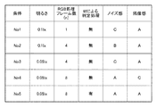
図10に本実施形態に係る撮像装置の評価結果を示す。画像の評価項目として、ノイズ感、残像感を用いた。動画像の偽色による妨害感は優れた評価から順に「A」、「B」、「C」と表記した。評価の条件として、明るさ、フレーム数n、フレーム判定処理の有無を変化させ、評価を行った。ここで、フレーム数nは、フレーム間処理の係数1/n、(n−1)/nにおける「n」を表している。また、フレーム判定処理はW画素の空間平均値Waveに基づく判定を表している。
FIG. 10 shows an evaluation result of the imaging apparatus according to the present embodiment. As the evaluation items of the image, a feeling of noise and a feeling of afterimage were used. The disturbing feeling due to the false color of the moving image is described as “A”, “B”, and “C” in order from the excellent evaluation. Evaluation was performed by changing the brightness, the number of frames n, and the presence / absence of the frame determination process as evaluation conditions. Here, the number n of frames represents “n” in the
条件No1として、周囲明るさを0.1[lx]とし、フレーム数n=1、判定処理無しとした。撮影された画像において、色が滲んだように見える色残像はないが、色ノイズが不快な程度目立ち、良好な画質とは言えなかった。従って、ノイズの評価は「C」、残像の評価は「A」であった。 As condition No. 1, the surrounding brightness was set to 0.1 [lx], the number of frames was set to n = 1, and no determination process was performed. In the photographed image, there is no color afterimage that looks like the color is blurred, but the color noise is conspicuous to the extent that it is unpleasant, and the image quality cannot be said to be good. Therefore, the evaluation of the noise was "C" and the evaluation of the afterimage was "A".
条件No2として、周囲明るさを0.1[lx]とし、フレーム数n=4、判定処理無しとした。撮影された画像において、色残像は多少目立つが、許容できる程度であった。色ノイズは目立つものの我慢できるレベルであった。従って、ノイズの評価は「B」、残像の評価は「A」であった。 As condition No. 2, the ambient brightness was 0.1 [lx], the number of frames was n = 4, and no determination processing was performed. In the captured image, color afterimages were somewhat conspicuous, but were acceptable. The color noise was noticeable but at a tolerable level. Therefore, the evaluation of the noise was "B" and the evaluation of the afterimage was "A".
条件No3として、周囲明るさを0.05[lx]とし、フレーム数n=4、判定処理無しとした。撮影された画像において、色残像は許容できる程度であったが、色ノイズは不快な程度となり、良好な画質を得ることはできなかった。従って、ノイズの評価は「C」、残像の評価は「A」であった。 As condition No. 3, the ambient brightness was set to 0.05 [lx], the number of frames was set to n = 4, and no determination process was performed. In the captured image, color afterimages were acceptable, but color noise was unpleasant, and good image quality could not be obtained. Therefore, the evaluation of the noise was "C" and the evaluation of the afterimage was "A".
条件No4として、周囲明るさを0.05[lx]とし、フレーム数n=8、判定処理無しとした。撮影された画像において、色ノイズは許容できる程度であった。ところが、平均化するフレーム数を増やしたことにより、色残像が目立ち、画質は不快なものとなった。従って、ノイズの評価は「A」、残像の評価は「C」であった。 As condition No. 4, the ambient brightness was set to 0.05 [lx], the number of frames was set to n = 8, and no determination process was performed. Color noise was acceptable in the captured image. However, by increasing the number of frames to be averaged, color afterimages were conspicuous and the image quality was uncomfortable. Therefore, the evaluation of the noise was "A" and the evaluation of the afterimage was "C".
条件No5として、周囲明るさ0.05[lx]とし、フレーム数n=8、判定処理有とした。撮影された画像において、色ノイズ、色残像共に許容できる程度であった。従って、ノイズの評価、残像の評価はともに「A」であった。 As condition No5, the ambient brightness was 0.05 [lx], the number of frames was n = 8, and the determination process was performed. In the photographed image, both color noise and color afterimage were acceptable. Therefore, both the evaluation of the noise and the evaluation of the afterimage were “A”.
以上説明したように、本実施形態によれば、RGBのベイヤ配列に代えて、W画素を有するCFを用いることによって、高感度の撮像装置を実現することが可能となる。また、人間の視覚特性は、色の時間的変化に対してさほど敏感ではないため、色信号をフレーム間処理し、ノイズリダクションを行うことによって、色ノイズを低減することができる。また、時間変化の大きい部分については、ノイズリダクションを行わない判定を行うことにより、動画の解像度を保ちつつ、色ノイズ、色残像を低減することができる。さらに、フレームの判定処理は、高解像度のW画素に基づき行われるため、判定の精度を高めることも可能となる。 As described above, according to this embodiment, a high-sensitivity imaging device can be realized by using a CF having W pixels instead of the RGB Bayer array. In addition, since human visual characteristics are not so sensitive to temporal changes in color, color noise can be reduced by performing inter-frame processing on color signals and performing noise reduction. In addition, for a portion having a large time change, it is possible to reduce the color noise and the color afterimage while maintaining the resolution of the moving image by performing the determination that the noise reduction is not performed. Furthermore, since the frame determination process is performed based on high-resolution W pixels, it is possible to increase the accuracy of the determination.
一般に、高感度化を図るために、ある小領域おいてW画素の割合を増やすと、RGB画素の割合が減少し、色ノイズが増加する。これは以下の様に説明される。各画素に発生するノイズは、フォトショットノイズと読出しノイズが合算されたものであるが、いずれもポアソン分布に従う特徴を持っている。従って、小領域の標準偏差は、画素数Nの平方根に比例する。一方、ある小領域の平均値は画素数Nに比例する。よって、S/N比は画素数Nの平方根に比例することになり、画素数が多いほどS/N比が大きい、すなわちノイズ感が小さい画像を得ることができる。画素数の少ないRGB画素においては、色ノイズが増加し易いが、本実施形態によればフレーム間処理により色ノイズを効果的に低減することが可能となる。また、動きの大きな被写体に応じて、フレーム間処理の重み付けを変更することにより、色残像も低減することができる。 In general, when the ratio of W pixels is increased in a certain small area in order to increase the sensitivity, the ratio of RGB pixels is reduced, and the color noise is increased. This is explained as follows. The noise generated in each pixel is a sum of the photo shot noise and the readout noise, and each has a characteristic according to a Poisson distribution. Therefore, the standard deviation of the small area is proportional to the square root of the number N of pixels. On the other hand, the average value of a certain small area is proportional to the number N of pixels. Therefore, the S / N ratio is proportional to the square root of the number N of pixels. As the number of pixels increases, an image having a higher S / N ratio, that is, an image with a small noise feeling can be obtained. In the case of RGB pixels having a small number of pixels, color noise tends to increase, but according to the present embodiment, color noise can be effectively reduced by inter-frame processing. Further, by changing the weight of the inter-frame processing according to the subject having a large motion, the color afterimage can be reduced.
なお、フレーム間処理は、IIRフィルタに限定されるものではなく、非巡回型フィルタ(FIR)を用いても良く、フレーム間移動平均、またはメディアンフィルタを用いても良い。さらに、フレーム間処理のフレーム数nは1、4、8などのように固定値に限定されず、nの値を被写体の環境(明るさ、コントラスト、被写体の移動速度等)に応じて適宜変更する適応型フィルタを用いても良い。フレーム間処理に用いられるフレームは、隣接するフレームに限定されず、2フレーム毎、3フレーム毎のように複数フレーム毎であっても良い。さらに、3フレーム以上のフレーム間における3点以上の画素値の傾きを用いて、フレーム間の変動量(差分、相関値)を算出してもよい。
なお、本実施例では、輝度信号処理部204、色信号処理部206が撮像素子1の外部に設けられた例を説明した。他の例として、撮像素子1が、輝度信号処理部204と色信号処理部206を有していても良い。また、撮像素子1が、撮像領域101が形成された第1の半導体基板と、輝度信号処理部204と色信号処理部206のそれぞれが形成された第2の半導体基板とが積層された積層型センサであっても良い。
The inter-frame processing is not limited to the IIR filter, and may use a non-recursive filter (FIR), a moving average between frames, or a median filter. Further, the number of frames n in the inter-frame processing is not limited to a fixed value such as 1, 4, 8, etc., and the value of n is appropriately changed according to the environment of the subject (brightness, contrast, moving speed of the subject, etc.). Alternatively, an adaptive filter may be used. The frames used for the inter-frame processing are not limited to adjacent frames, and may be every two or three frames. Furthermore, the variation amount (difference, correlation value) between frames may be calculated using the inclination of three or more pixel values between three or more frames.
In the present embodiment, an example in which the luminance
(第2の実施形態)
図11は、本実施形態に係る撮像装置の信号処理部2のブロック図である。第1実施形態はWの画素値の平均値Waveに基づきフレーム間処理の判定を行っていたが、本実施形態は色比情報に基づきフレーム間処理の判定を行う。以下、第2実施形態の撮像装置について、第1の実施形態とは異なる点を中心に説明する。
(Second embodiment)
FIG. 11 is a block diagram of the
制御部205は色比処理部222、判定処理部213を備え、色比処理部222には補間後のWの画素信号3cとRGBの画素信号3eが入力される。
The
色比処理部222は、補間したiWr、iWg、iWbの画素値とRGBの画素値とのそれぞれの比を算出し、色比情報を出力する。色比は、R/iWr、G/iWg、B/iWbの式に従い算出される。
The color
判定処理部213は、色比情報のフレーム間差分の絶対値と閾値Vthとを比較し、比較結果に基づく判定信号Jを出力する。例えば、色比B/iWbに基づく判定信号Jは次式に従い求められる。
ここで、B(N)、iWb(N)は第NフレームのBの画素値、iWbの画素値を表し、B(N−1)、iWb(N−1)は第(N−1)フレームのBの画素値、iWbの画素値を表している。R、Gの画素値についても同様に判定信号Jを求めることができる。この場合、RGBのそれぞれについて判定信号Jを求め、フレーム間処理の重み付けを変更することができる。また、差分絶対値が最大となる色比に基づき判定信号Jを決定しても良く、さらには、色比の平均値を用いて判定信号Jを決定しても良い。閾値Vthは1以下の値であって、様々な被写体の撮像結果に基づき最適な値に設定されることが望ましい。なお、被写体照度、照明の色温度などの撮影条件に基づき、閾値Vthを動的に変更させても良い。 Here, B (N) and iWb (N) represent the pixel value of B and iWb in the Nth frame, and B (N-1) and iWb (N-1) represent the (N-1) th frame. B and iWb. The determination signal J can be similarly obtained for the R and G pixel values. In this case, the determination signal J is obtained for each of RGB, and the weight of the inter-frame processing can be changed. Further, the determination signal J may be determined based on the color ratio at which the absolute difference value is maximum, and the determination signal J may be determined using the average value of the color ratio. The threshold value Vth is a value of 1 or less, and is desirably set to an optimum value based on the imaging results of various subjects. The threshold value Vth may be dynamically changed based on shooting conditions such as the illuminance of the subject and the color temperature of the illumination.
図12は本実施形態に係る制御部205、色信号処理部206の動作を説明するための図である。図12(a)は、各フレームのiWb、Bのそれぞれの画素値を表しており、図12(b)は、各フレームの色比情報を表している。これらの図は、図9と同様に、灰色の背景の前を青色の球体が移動する被写体の撮像結果を示しており、第(N−3)フレームから第Nフレームまでの領域900における各値の変化を示している。第(N−3)フレームから第(N−1)フレームにおいて、色比情報B/iWbの変化は小さいため、フレーム間の色比情報の差分絶対値は閾値Vth以下となる。よって、判定信号Jは「0」となり、フレーム間処理部214において色信号のフレーム間処理が行われ、色信号のノイズリダクションがなされる。第(N−1)フレームから第Nフレームにかけて、領域900が青色から灰色に変化すると、Bの画素値およびiWbの画素値の色比情報が変化する。フレーム間の色比情報B/iWbの差分絶対値が閾値Vthを超えると、判定信号Jは「1」となり、色信号のフレーム間処理は行われない。従って、過去フレームを参照することにより生じ得る色残像を抑制することができる。
FIG. 12 is a diagram for explaining operations of the
本実施形態は色比に基づきフレーム間処理の重み付けを変更しているため、Wの画素値に基づき重み付けを変更する第1実施形態に比べて演算処理量が増加し得るが、色残像を効果的に抑制することができる。色信号処理のフレーム間処理(ノイズリダクション)により、色残像が生じる主要な原因は、色比の急激な変化である。従って、色比の変化(差分)に応じて、色信号のフレーム間処理の可否を判定することにより、色残像を効果的に抑制することが可能となる。また、RGBW12配列においては、RGB画素はW画素によって囲まれているため、RGB画素位置におけるWの画素値を高精度に補間することができる。よって、色比を高精度に算出することができ、フレーム間処理の判定の精度を向上させることが可能となる。 Since the weight of the inter-frame processing is changed based on the color ratio in the present embodiment, the amount of calculation processing can be increased as compared with the first embodiment in which the weight is changed based on the pixel value of W. Can be suppressed. A major cause of color afterimages due to inter-frame processing (noise reduction) of color signal processing is a rapid change in color ratio. Therefore, it is possible to effectively suppress color afterimages by determining whether or not to perform the inter-frame processing of the color signal according to the change (difference) of the color ratio. Further, in the RGBW12 array, since the RGB pixels are surrounded by the W pixels, the pixel values of W at the RGB pixel positions can be interpolated with high accuracy. Therefore, the color ratio can be calculated with high accuracy, and the accuracy of the determination of the inter-frame processing can be improved.
以上説明したように、本実施形態によれば、色比を用いて色信号のフレーム間処理における各フレームの重み付けを変更している。色比を判定に用いることで、本来の色比から離れたフレーム間処理がなされることを回避し、色付きの残像が生じるのを高精度に防止することができる。すなわち、第1の実施形態と比較して、フレーム間処理の判定をさらに高精度に行うことができ、色残像をさらに低減することが可能となる。 As described above, according to the present embodiment, the weighting of each frame in the inter-frame processing of the color signal is changed using the color ratio. By using the color ratio for determination, it is possible to avoid performing inter-frame processing that is different from the original color ratio, and to prevent the occurrence of colored afterimages with high accuracy. That is, compared with the first embodiment, the determination of the inter-frame processing can be performed with higher accuracy, and the color afterimage can be further reduced.
なお、フレーム間処理の判定において、色比に代えて、iWの画素値とRGBの画素値との色差を用いてもよい。すなわち、フレーム間において色差が閾値Vth以下である場合には、色信号のフレーム間処理を実行し、フレーム間の色差が閾値Vthを超えた場合には、色信号のフレーム間処理を実行しないように構成しても良い。 In the determination of the inter-frame processing, the color difference between the pixel value of iW and the pixel value of RGB may be used instead of the color ratio. That is, if the color difference between the frames is equal to or less than the threshold value Vth, the inter-frame processing of the color signal is executed. If the color difference between the frames exceeds the threshold value Vth, the inter-frame processing of the color signal is not executed. May be configured.
(第3の実施形態)
図13は、本実施形態に係る撮像装置の信号処理部2のブロック図である。本実施形態は、W画素の複数フレームを用いた動きベクトルに基づきフレーム間処理の判定を行う点において第1実施形態と異なっている。以下、本実施形態に係る撮像装置について、第1実施形態とは異なる点を中心に説明する。
(Third embodiment)
FIG. 13 is a block diagram of the
判定処理部231はブロックマッチング法により動きベクトルを算出し、動きベクトルの絶対値と閾値Vthとの比較結果に基づき判定信号Jを決定する。
The
図14は本実施形態に係る判定処理部231の動作を説明するための図であって、ブロックマッチング法における基準フレームおよび参照フレームを示している。図14(a)において、判定処理部231は、基準フレーム内に窓領域Aを設定し、窓領域A内のパターンと類似するパターンを参照フレーム内で探索する。参照フレームとして、第(N−1)フレームの次の第Nフレームが用いられる。
FIG. 14 is a diagram for explaining the operation of the
探索範囲は、図14(b)に示すように、通常、移動量ゼロの位置Bを基準とした所定の範囲Cが設定される。また、パターンの類似度は、次式で表される残差平方和SSD(Sum of Squared Difference)を評価値として判断し得る。
![]()
![]()
ここで、f(x、y、t)は画像の時空間分布であり、x、y∈Wは、基準フレームの窓領域内に含まれる画素の座標値を意味する。 Here, f (x, y, t) is a spatio-temporal distribution of the image, and x, y∈W means a coordinate value of a pixel included in the window region of the reference frame.
判定処理部231は、探索範囲内で(u、v)を変化させることにより、評価値が最小となる(u、v)の組を探索し、この(u、v)をフレーム間の動きベクトルとする。判定処理部213は、窓領域の位置を順次シフトさせることによって、動きベクトルを画素毎もしくはブロック毎(例えば8画素×8画素)に求める。
The
RGB画素に比べて、画素数が多く、感度が高いW画素を動き検知に用いることにより、動きベクトルの空間解像度を上げるとともに、動きベクトルの算出におけるノイズに対する耐性を高めることが可能となる。 By using W pixels having a larger number of pixels and higher sensitivity as compared with the RGB pixels for motion detection, it is possible to increase the spatial resolution of the motion vector and increase the resistance to noise in the calculation of the motion vector.
動きベクトルの絶対値が閾値Vthを越えた場合には、判定処理部213は判定信号Jを「1」とする。この場合、フレーム間処理部214は、色信号のフレーム間処理の処理数を少なくし、あるいは、フレーム間処理を行わない。これにより、動きのある部分に色信号処理を行うことにより生じる色残像を低減することが可能となる。一方、動きベクトルの絶対値が閾値Vth以下の場合には、判定信号Jは「0」となり、フレーム間処理部214において色信号のフレーム間処理が行われ、色信号のノイズリダクションがなされる。
When the absolute value of the motion vector exceeds the threshold value Vth, the
本実施形態においても、第1、第2の実施形態と同様の効果を奏することが可能である。さらに、本実施形態においては、W画素における動きベクトルの大きさに応じて色信号のフレーム間処理を行うか否かを判定している。W画素は高い空間解像度と高い感度を有していることから、フレーム間処理の判定を高精度に行うことができる。この結果、色残像をさらに低減しながら、色信号のノイズリダクション効果を得ることが可能となる。 Also in the present embodiment, it is possible to achieve the same effects as in the first and second embodiments. Further, in the present embodiment, it is determined whether or not to perform the inter-frame processing of the color signal according to the magnitude of the motion vector in the W pixel. Since the W pixel has a high spatial resolution and a high sensitivity, the determination of the inter-frame processing can be performed with high accuracy. As a result, it is possible to obtain a color signal noise reduction effect while further reducing color afterimages.
(第4の実施形態)
図15は、本実施形態に係る撮像装置の信号処理部2のブロック図である。本実施形態の撮像装置は、図4(c)で表わされるRGBW8配列を用いている点において第1実施形態の撮像装置と異なっている。以下、第4実施形態の撮像装置について、第1実施形態と異なる点を中心に説明する。
(Fourth embodiment)
FIG. 15 is a block diagram of the
RGBW8の配列においては、RGBW12の配列に比べてW画素が少ないため、感度が低下する。一方、W画素の周囲にRGBの画素が存在するため、偽色が発生し難くなる。図15において、RGBW8のCF配列の画素信号4aは、輝度信号であるWの画素信号4bと、色信号であるRGBの画素信号4eとに分離される。
In the arrangement of RGBW8, the sensitivity is reduced because there are fewer W pixels than in the arrangement of RGBW12. On the other hand, since RGB pixels exist around the W pixels, false colors are less likely to occur. In FIG. 15, the pixel signal 4a of the RGBW8 CF array is separated into a
輝度信号処理部204は、画素信号4bにおいてRGB画素を分離した部分の画素値を補間処理によって求め、補間後の画素信号4cを生成する。補間された画素はiWr、iWg、iWbと表記されている。
The luminance
制御部205は空間平均処理部212、判定処理部213を備える。空間平均処理部212はWの画素信号4bにおいて所定ブロックの画素値の平均値Waveを算出する。判定処理部213は平均値Waveのフレーム間の差分と閾値Vthとを比較する。フレーム間差分の絶対値が閾値Vthより大きい場合は、判定信号Jは「1」となり、フレーム間差分の絶対値が閾値Vth以下の場合は、判定信号Jは「0」となる。
色信号処理部206はフレーム間処理部214を備える。フレーム間処理部214の処理は第1実施形態と同様に構成されている。すなわち、判定信号Jが「1」の場合、フレーム間処理部214は色信号のフレーム間処理の処理数を少なくし、またはフレーム間処理を行わない。つまり、Wの画素値の時間的変化が大きい場合、色信号のフレーム間処理を少なくすることにより、動きのある被写体の色残像を低減することが可能となる。
The color
信号合成部207は、補間後のWの画素信号4cと、色信号処理後のRGBの画素信号とを合成する。すなわち、信号合成部207は、W、iWの画素値と、同位置のn_R、n_G、n_Bの画素値との色比を算出し、色比とW、iWの画素値とを乗算することにより、画素毎にRGBの値を算出する。第1実施形態と同様に、W、iWの画素のそれぞれについてRGBの画素値は次式で求められる。
本実施形態においては、RGBW8の配列を用いることにより、第1の実施形態に比べて、画像の感度、解像度が低くなったが、被写体の絵柄によっては偽色を低減することができた。 In the present embodiment, by using the arrangement of RGBW8, the sensitivity and resolution of the image are lower than in the first embodiment, but false colors can be reduced depending on the pattern of the subject.
(第5の実施形態)
図16は本実施形態に係る撮像装置の信号処理部2のブロック図である。本実施形態の撮像装置は、図4(d)で表わされるRGBG12の配列を用いている点において第1実施形態の撮像装置と異なっている。以下、第5実施形態の撮像装置について、第1実施形態と異なる点を中心に説明する。
(Fifth embodiment)
FIG. 16 is a block diagram of the
RGBG12の配列においては、RGBW12のW画素をG画素に置き換えているため、感度が低下し易い。しかしながら、Wの画素はRGB画素に対して感度が高いため、高輝度の被写体を撮像した際に、W画素が飽和し、ダイナミックレンジが低下し得る。本実施形態において、RGBG12配列のCFを用いることにより、信号の飽和と感度のバランスを取ることができる。 In the RGBG12 array, the W pixels of the RGBW12 are replaced with G pixels, so that the sensitivity is likely to decrease. However, since the W pixel has high sensitivity to the RGB pixels, when capturing a high-luminance subject, the W pixel may be saturated and the dynamic range may be reduced. In the present embodiment, by using CFs in the RGBG12 arrangement, it is possible to balance signal saturation and sensitivity.
図16において、画素信号5aはGの画素信号5bとR、Bの画素信号5eとに分離される。
In FIG. 16, a pixel signal 5a is separated into a
輝度信号処理部204は画素信号5bにおいてR、Bの画素が分離された部分の補間処理を行い、iGr、iGbの画素値を生成する。空間平均処理部212はGの画素信号5bにおいて所定ブロックのGの画素値の平均値Waveを算出する。判定処理部213は平均値Waveのフレーム間の差分と閾値Vthとを比較する。フレーム間差分の絶対値が閾値Vthより大きい場合は、判定信号Jは「1」となり、フレーム間差分の絶対値が閾値Vth以下の場合は、判定信号Jは「0」となる。
G画素の感度はW画素の感度に比べて低いものの、G画素はR、B画素に比べて輝度情報を多く含む。被写体が動いた場合には、色だけではなく輝度が変化する場合が多い。このため、G画素のフレーム間の差分を求めることで、フレーム間処理の判定精度を上げることができる。 Although the sensitivity of the G pixel is lower than the sensitivity of the W pixel, the G pixel contains more luminance information than the R and B pixels. When the subject moves, not only the color but also the luminance often changes. For this reason, by determining the difference between the frames of the G pixels, the determination accuracy of the inter-frame processing can be improved.
色信号処理部206は、R、Bの画素信号5eのフレーム間処理を行う。フレーム間処理部214の処理は第1実施形態と同様である。フレーム間処理部214は、判定信号Jが「1」の場合は、判定信号Jが「0」の場合に比べて、フレーム間処理の処理数を少なくし、またはフレーム間処理を行わない。すなわち、Gの画素値の時間変化が大きい場合には、色信号のフレーム間処理を少なくする。これにより、動きのある被写体において、色づきの残像を低減することが可能となる。
The color
信号合成部207は、補間後のGの画素信号5cと、フレーム間処理後のR、Bの画素信号を合成する。すなわち、信号合成部207はG、iGの画素値と、同位置のn_R、n_Bの画素値との色比を算出し、色比とG、iGの画素値とを乗算することにより、画素毎にRGBの値を算出する。G、iGの画素のそれぞれについてRGBの画素値は次式で求められる。
撮影した画像において、第1の実施形態に比べ、感度、解像度が低くなったが、RGB画素を用いることにより、飽和を抑えるとともに、動画撮影時の偽色を低減することが可能となった。このように、輝度信号は第1の実施形態のようにW画素の信号に限定されず、視覚特性において輝度情報が多く含まれる画素(例えばG画素)の情報であればよい。また、色信号は、相対的に輝度情報の少ない画素(例えばR画素、B画素)の信号であればよい。さらに、本実施形態は、画素信号5aをGの画素信号5bとR、Bの画素信号5eに分離しているが、輝度情報が多く含まれるデータと輝度情報の少ないデータとを演算によって分けても同様の効果を奏することができる。
Although the sensitivity and resolution of the captured image are lower than those of the first embodiment, the use of RGB pixels makes it possible to suppress saturation and reduce false colors at the time of capturing a moving image. As described above, the luminance signal is not limited to the signal of the W pixel as in the first embodiment, and may be information of a pixel (for example, a G pixel) including a large amount of luminance information in visual characteristics. Further, the color signal may be a signal of a pixel (for example, R pixel, B pixel) having relatively little luminance information. Further, in the present embodiment, the pixel signal 5a is separated into the
(第6の実施形態)
図17は本実施形態に係る撮像装置の信号処理部2のブロック図である。
(Sixth embodiment)
FIG. 17 is a block diagram of the
本実施形態の撮像装置について、第1の実施形態とは異なる点を中心に説明する。本実施形態において、撮像素子1は図5(b)で表されるCMYW12配列を用いている。CMYW12配列は感度の高い補色(C、M、Y)の画素に加えてさらにWの画素を用いていることから、感度を向上させることができる。
The imaging device according to the present embodiment will be described focusing on differences from the first embodiment. In the present embodiment, the
図17において、撮像素子1からの画素信号6aは、Wの画素信号6bと、C、M、Yの画素信号6eとに分離される。
In FIG. 17, a
輝度信号処理部204は、画素信号6bにおいて、C、M、Yの画素が分離された部分を補間処理し、iWc、iWm、iWyの画素値を生成する。制御部205の空間平均処理部212はWの画素信号6bにおいて所定のブロックの画素値の平均値Waveを算出する。判定処理部213は平均値Waveのフレーム間の差分と閾値Vthとを比較する。フレーム間差分の絶対値が閾値Vthより大きい場合は、判定信号Jは「1」となり、フレーム間差分の絶対値が閾値Vth以下の場合は、判定信号Jは「0」となる。
色信号処理部206のフレーム間処理部214は第2の画素群であるCMYの画素信号のフレーム間処理を行う。フレーム間処理部214は、判定信号Jが「1」の場合は、判定信号Jが「0」の場合よりも、フレーム間処理の処理数を少なくし、またはフレーム間処理を行わない。これにより、動きのある被写体の動きがある場合における色付きの残像を低減することが可能となる。信号合成部207は、補間後のWの画素信号6cと、色信号処理後のCMYの画素信号とを合成する。すなわち、信号合成部207は、W、iWの画素値と、同位置のn_C、n_M、n_Yの画素値との色比を算出し、色比とW、iWの画素値とを乗算することにより、画素毎にCMYの値を算出する。W、iWの画素のそれぞれについてCMYの画素値は次式で求められる。
CMY/RGB変換部287は、信号合成部207から出力されたCMYの画素値をRGBの画素値に変換し、画像信号6gを出力する。以上の処理を行った撮像装置を用いて評価撮影を行った。一部画像パターンにおいて色再現性が劣るものの、第1の実施形態の撮像装置に比べて感度が高くなり、動画撮影時の偽色が低減された。なお、信号合成部207の処理をCMY/RGB変換部287の処理の後に実行してもよく、また、2つの処理を一体として実行してもよい。
The CMY /
(第7の実施形態)
図18は本実施形態の撮像装置の信号処理部2のブロック図である。本実施形態の撮像装置について、第1の実施形態と異なる点を中心に説明する。本実施形態において、撮像素子1は図4(a)で表わされるベイヤ(RGB)配列を用いている。輝度信号処理部204はGの画素値を輝度信号として処理を行い、色信号処理部206はR、Bの画素値を色信号として処理を行う。ベイヤ配列においては、W画素を用いたCFに比べると感度が低いという性質を有している。しかしながら、本実施形態によれば、比較的感度の低いR、Bの画素値に対してフレーム間処理を行うことにより、低照度時の色ノイズを抑えることができる。また、R、Bの画素と比較して感度および解像度の高いG画素を用いてフレーム間処理の判定を行うことで、判定精度を向上させ、色残像を低減することができる。
(Seventh embodiment)
FIG. 18 is a block diagram of the
図18において、ベイヤ(RGB)配列の画素信号7aは、Gの画素信号7bと、RBの画素信号7eとに分離される。
In FIG. 18, a pixel signal 7a in a Bayer (RGB) arrangement is separated into a
輝度信号処理部204はR、Bの画素が分離された部分を補間処理し、iGr、iGbの画素値を生成する。制御部205の空間平均処理部212はGの画素信号7bにおいて所定ブロックの画素値の平均値Gaveを算出する。判定処理部213は、G画素の空間平均値をフレーム間差分し、閾値Vthと比較する。フレーム間の差分絶対値が閾値Vthより大きい場合は、判定信号Jは「1」となり、フレーム間の差分絶対値が閾値Vth以下の場合は、判定信号Jは「0」となる。
色信号処理部206は、RBの画素信号7eのフレーム間処理を行う。すなわち、フレーム間処理部214は、判定信号Jが「1」の場合は、判定信号「J」が0の場合よりも、フレーム間処理の処理数を少なくし、またはフレーム間処理を行わない。つまり、Gの画素値の時間的変化が大きい場合には、色信号のフレーム間処理を少なくする。これにより、動きのある被写体において、色残像を低減することが可能となる。
The color
信号合成部207では、補間後のGの画素信号7cと、フレーム間処理後のRBの画素信号とを合成する。信号合成部207はG、iGの画素値と、同位置のn_R,n_Bの画素値との色比を算出し、色比とG、iGの画素値とを乗算する。よって、画素毎にRGBの値が算出され、画像信号7gが生成される。G、iGの画素のそれぞれについてRGBの画像値は次式で求められる。
![]()
![]()
![]()
![]()
撮影した画像において、ベイヤ配列のCFを用いながら、低照度での色ノイズの低減、および色残像の低減を両立することが可能となった。 In a captured image, it has become possible to achieve both a reduction in color noise at low illuminance and a reduction in color afterimage while using CF in a Bayer array.
(第8の実施形態)
第8の実施形態に係る撮像システムを説明する。上述した第1〜第7の実施形態の撮像装置は種々の撮像システムに適用可能である。撮像システムは撮像装置を用いて画像、動画等を取得する装置であり、その一例としては、デジタルスチルカメラ、デジタルカムコーダー、監視カメラなどがある。図19に、撮像システムの例としてデジタルスチルカメラに第1〜第7の実施形態の撮像装置を適用したブロック図を示す。
(Eighth embodiment)
An imaging system according to the eighth embodiment will be described. The imaging devices of the first to seventh embodiments described above are applicable to various imaging systems. An imaging system is a device that acquires an image, a moving image, and the like using an imaging device, and examples thereof include a digital still camera, a digital camcorder, and a surveillance camera. FIG. 19 shows a block diagram in which the imaging devices of the first to seventh embodiments are applied to a digital still camera as an example of an imaging system.
図19において、撮像システムは被写体の光学像を撮像装置301に結像させるレンズ302、レンズ302の保護のためのバリア303およびレンズ302を通った光量を調整するための絞り304を有する。また、撮像システムは撮像装置301より出力される出力信号の処理を行う出力信号処理部305を有する。
19, the imaging system includes a
出力信号処理部305はデジタル信号処理部を有し、撮像装置301から出力される信号を、必要に応じて各種の補正、圧縮を行って信号を出力する動作を行う。撮像装置301から出力される信号がアナログ信号である場合、出力信号処理部305はアナログ/デジタル変換回路をデジタル信号処理部の前段に備えてもよい。
The output
また、撮像システムは、画像データを一時的に記憶するためのバッファメモリ部306、記録媒体への記録または読み出しを行うための記憶媒体制御インターフェース(I/F)部307を有する。さらに撮像システムは、撮像データの記録または読み出しを行うための半導体メモリ等の、着脱可能な、または撮像システムに内蔵された、記録媒体309を有する。さらに、撮像システムは、外部のコンピュータ等と通信するための外部インターフェース(I/F)部308、各種演算とデジタルスチルカメラ全体を制御する全体制御・演算部310を有する。さらに撮像システムは、出力信号処理部305に、各種タイミング信号を出力するタイミング発生部311を有する。なお、タイミング信号などの制御信号はタイミング発生部311ではなく外部から入力されてもよい。すなわち、撮像システムは少なくとも撮像装置301と、撮像装置301から出力された出力信号を処理する出力信号処理部305とを有すればよい。
Further, the imaging system includes a
以上のように、本実施形態の撮像システムは、第1〜第7の実施形態で述べた撮像装置301を適用して撮像動作を行うことが可能である。
As described above, the imaging system of this embodiment can perform an imaging operation by applying the
(他の実施形態)
以上、本発明に係る撮像装置を説明したが、本発明は上述の実施形態に限定されるものではなく、本発明の趣旨を逸脱しない範囲で適宜修正および変形することを妨げるものではない。例えば、上述の第1〜第8実施形態の構成を組み合わせることも可能である。また、撮像装置は必ずしも撮像素子を備えなくても良く、撮像素子から出力された画像信号を処理するコンピュータなどの画像処理システムであっても良い。
(Other embodiments)
As described above, the imaging apparatus according to the present invention has been described, but the present invention is not limited to the above-described embodiment, and does not prevent appropriate modification and deformation without departing from the spirit of the present invention. For example, the configurations of the above-described first to eighth embodiments can be combined. Further, the imaging device does not necessarily need to include an imaging device, and may be an image processing system such as a computer that processes an image signal output from the imaging device.
1 撮像素子
2 信号処理部
100 画素
204 輝度信号処理部
205 制御部
206 色信号処理部
207 信号合成部
Claims (28)
前記撮像素子は、画素信号を各々が出力する複数の画素を各々が備える第1の画素群と第2の画素群とを有し、前記第2の画素群の複数の第2の画素が出力する第2の画素信号が含む解像度情報は前記第1の画素群の複数の第1の画素が出力する第1の画素信号が含む解像度情報よりも少なく、
前記信号処理部は、前記第2の画素から出力された第2の画素信号をフレーム間処理によって重み付け加算するとともに、同一の前記第1の画素から出力される複数のフレームの前記第1の画素信号のフレーム間の差分に基づいて前記重み付け加算における各フレームの重み付けを変更することを特徴とする撮像装置。 An image pickup device including an image pickup device and a signal processing unit,
The image sensor has a first pixel group and a second pixel group each including a plurality of pixels each outputting a pixel signal, and a plurality of second pixels of the second pixel group are output. The resolution information included in the second pixel signal is smaller than the resolution information included in the first pixel signal output by the plurality of first pixels of the first pixel group,
The signal processing unit weights and adds a second pixel signal output from the second pixel by inter-frame processing, and the first pixel of a plurality of frames output from the same first pixel An imaging apparatus, wherein the weighting of each frame in the weighted addition is changed based on a difference between signal frames.
前記撮像素子は、それぞれが光電変換部を有する第1の画素および第2の画素を備え、The imaging device includes a first pixel and a second pixel each having a photoelectric conversion unit,
前記第1の画素は、前記光電変換部において白に対応した光に基づき第1の画素信号を出力可能に構成され、The first pixel is configured to be able to output a first pixel signal based on light corresponding to white in the photoelectric conversion unit,
前記第2の画素は、前記光電変換部において緑、青、および赤のいずれかに対応する光に基づき第2の画素信号を出力可能に構成され、The second pixel is configured to be capable of outputting a second pixel signal based on light corresponding to one of green, blue, and red in the photoelectric conversion unit,
前記第1の画素は、第1フレーム、第2フレームのそれぞれにおいて、前記第1の画素信号を出力し、The first pixel outputs the first pixel signal in each of a first frame and a second frame,
前記第2の画素は、前記第1フレーム、前記第2フレームのそれぞれにおいて、前記第2の画素信号を出力し、The second pixel outputs the second pixel signal in each of the first frame and the second frame,
前記信号処理部は、前記第1フレームの前記第2の画素信号と前記第2フレームの前記第2の画素信号の加算であるフレーム間処理とを実行し、The signal processing unit executes an inter-frame process that is an addition of the second pixel signal of the first frame and the second pixel signal of the second frame,
前記信号処理部は、同一の前記第1の画素における前記第1フレームの前記第1の画素信号と前記第2フレームの前記第1の画素信号との差に基づいて、前記フレーム間処理を、前記第1フレームの前記第2の画素信号と前記第2フレームの前記第2の画素信号の重み付けを変更して行うことを特徴とする撮像装置。The signal processing unit performs the inter-frame processing based on a difference between the first pixel signal of the first frame and the first pixel signal of the second frame in the same first pixel. An image pickup apparatus, wherein weighting is performed on the second pixel signal of the first frame and the second pixel signal of the second frame.
前記撮像素子は、それぞれが光電変換部を有する第1の画素および第2の画素を備え、The imaging device includes a first pixel and a second pixel each having a photoelectric conversion unit,
前記第1の画素は、前記光電変換部において白に対応した光に基づき第1の画素信号を出力可能に構成され、The first pixel is configured to be able to output a first pixel signal based on light corresponding to white in the photoelectric conversion unit,
前記第2の画素は、前記光電変換部においてシアン、マゼンダ、およびイエローのいずれかに対応する光に基づき第2の画素信号を出力可能に構成され、The second pixel is configured to output a second pixel signal based on light corresponding to any of cyan, magenta, and yellow in the photoelectric conversion unit,
前記第1の画素は、第1フレームおよび第2フレームのそれぞれにおいて、前記第1の画素信号を出力し、The first pixel outputs the first pixel signal in each of a first frame and a second frame,
前記第2の画素は、前記第1フレームおよび前記第2フレームのそれぞれにおいて、前記第2の画素信号を出力し、The second pixel outputs the second pixel signal in each of the first frame and the second frame;
前記信号処理部は、前記第1フレームの前記第2の画素信号と前記第2フレームの前記第2の画素信号の加算であるフレーム間処理とを実行し、The signal processing unit executes an inter-frame process that is an addition of the second pixel signal of the first frame and the second pixel signal of the second frame,
前記信号処理部は、同一の前記第1の画素における前記第1フレームの前記第1の画素信号と前記第2フレームの前記第1の画素信号との差に基づいて、前記フレーム間処理を、前記第1フレームの前記第2の画素信号と前記第2フレームの前記第2の画素信号の重み付けを変更して行うことを特徴とする撮像装置。The signal processing unit performs the inter-frame processing based on a difference between the first pixel signal of the first frame and the first pixel signal of the second frame in the same first pixel. An image pickup apparatus, wherein weighting is performed on the second pixel signal of the first frame and the second pixel signal of the second frame.
を有することを特徴とする撮像システム。 An imaging device according to any one of claims 1 to 24, and an output signal processing unit that processes a signal output by the imaging device,
An imaging system comprising:
前記撮像素子は、前記画素信号を各々が出力する複数の画素を各々が備える第1の画素群と第2の画素群とを有し、前記第2の画素群の複数の第2の画素が出力する第2の画素信号が含む解像度情報は前記第1の画素群の複数の第1の画素が出力する第1の画素信号が含む解像度情報よりも少なく、
前記画像処理方法は、前記第2の画素から出力された第2の画素信号をフレーム間処理によって重み付け加算するとともに、同一の前記第1の画素から出力される複数のフレームの前記第1の画素信号のフレーム間の差分に基づいて前記重み付け加算における各フレームの重み付けを変更することを特徴とする画像処理方法。 An image processing method for processing a pixel signal output by an imaging device including an imaging device and a signal processing unit,
The image sensor has a first pixel group and a second pixel group each including a plurality of pixels each outputting the pixel signal, and a plurality of second pixels of the second pixel group are The resolution information included in the output second pixel signal is smaller than the resolution information included in the first pixel signal output from the plurality of first pixels of the first pixel group,
In the image processing method, the second pixel signal output from the second pixel is weighted and added by inter-frame processing, and the first pixel of a plurality of frames output from the same first pixel is added. An image processing method, wherein weighting of each frame in the weighted addition is changed based on a difference between signal frames.
前記第2の画素群の複数の第2の画素が出力する第2の画素信号が含む解像度情報は前記第1の画素群の複数の第1の画素が出力する第1の画素信号が含む解像度情報よりも少なく、
前記信号処理部は、前記第2の画素から出力された第2の画素信号をフレーム間処理によって重み付け加算するとともに、同一の前記第1の画素から出力される複数のフレームの前記第1の画素信号のフレーム間の差分に基づいて前記重み付け加算における各フレームの重み付けを変更することを特徴とする撮像素子。 An image sensor having a first pixel group, a second pixel group, each including a plurality of pixels each outputting a pixel signal, and a signal processing unit,
The resolution information included in the second pixel signals output by the plurality of second pixels of the second pixel group is the resolution included in the first pixel signals output by the plurality of first pixels of the first pixel group. Less than information,
The signal processing unit weights and adds a second pixel signal output from the second pixel by inter-frame processing, and the first pixel of a plurality of frames output from the same first pixel An image sensor, wherein the weight of each frame in the weighted addition is changed based on a difference between signal frames.
第2の半導体基板に前記信号処理部が形成され、
前記第1の半導体基板と前記第2の半導体基板とが積層されていることを特徴とする請求項27に記載の撮像素子。 The first pixel group and the second pixel group are formed on a first semiconductor substrate;
The signal processing unit is formed on a second semiconductor substrate;
The imaging device according to claim 27, wherein the first semiconductor substrate and the second semiconductor substrate are stacked.
Priority Applications (3)
| Application Number | Priority Date | Filing Date | Title |
|---|---|---|---|
| JP2015101706A JP6628497B2 (en) | 2015-05-19 | 2015-05-19 | Imaging device, imaging system, and image processing method |
| US15/143,817 US9900532B2 (en) | 2015-05-19 | 2016-05-02 | Imaging apparatus, imaging system, and image processing method |
| US15/862,128 US10122951B2 (en) | 2015-05-19 | 2018-01-04 | Imaging apparatus, imaging system, and image processing method |
Applications Claiming Priority (1)
| Application Number | Priority Date | Filing Date | Title |
|---|---|---|---|
| JP2015101706A JP6628497B2 (en) | 2015-05-19 | 2015-05-19 | Imaging device, imaging system, and image processing method |
Publications (3)
| Publication Number | Publication Date |
|---|---|
| JP2016219977A JP2016219977A (en) | 2016-12-22 |
| JP2016219977A5 JP2016219977A5 (en) | 2018-06-28 |
| JP6628497B2 true JP6628497B2 (en) | 2020-01-08 |
Family
ID=57324927
Family Applications (1)
| Application Number | Title | Priority Date | Filing Date |
|---|---|---|---|
| JP2015101706A Active JP6628497B2 (en) | 2015-05-19 | 2015-05-19 | Imaging device, imaging system, and image processing method |
Country Status (2)
| Country | Link |
|---|---|
| US (2) | US9900532B2 (en) |
| JP (1) | JP6628497B2 (en) |
Families Citing this family (20)
| Publication number | Priority date | Publication date | Assignee | Title |
|---|---|---|---|---|
| JP6584131B2 (en) * | 2015-05-08 | 2019-10-02 | キヤノン株式会社 | Imaging apparatus, imaging system, and signal processing method |
| US9871965B2 (en) * | 2016-02-03 | 2018-01-16 | Texas Instruments Incorporated | Image processing for wide dynamic range (WDR) sensor data |
| JP6758859B2 (en) | 2016-03-01 | 2020-09-23 | キヤノン株式会社 | Imaging equipment, imaging system, and image processing methods |
| JP6436953B2 (en) | 2016-09-30 | 2018-12-12 | キヤノン株式会社 | Solid-state imaging device, driving method thereof, and imaging system |
| JP6732625B2 (en) | 2016-10-07 | 2020-07-29 | キヤノン株式会社 | Imaging device and imaging system |
| JP6865589B2 (en) | 2017-01-10 | 2021-04-28 | キヤノン株式会社 | Imaging device |
| JP6843682B2 (en) * | 2017-04-07 | 2021-03-17 | キヤノン株式会社 | Image sensor and image sensor |
| JP6980492B2 (en) * | 2017-11-13 | 2021-12-15 | キヤノン株式会社 | Imaging device and imaging system |
| KR102314647B1 (en) * | 2017-11-23 | 2021-10-19 | 삼성전자주식회사 | Method and device for processing an image and recording medium thereof |
| JP6953297B2 (en) | 2017-12-08 | 2021-10-27 | キヤノン株式会社 | Imaging device and imaging system |
| JP7075208B2 (en) | 2017-12-22 | 2022-05-25 | キヤノン株式会社 | Imaging equipment and imaging system |
| JP7157529B2 (en) | 2017-12-25 | 2022-10-20 | キヤノン株式会社 | Imaging device, imaging system, and imaging device driving method |
| JP7260990B2 (en) | 2018-10-26 | 2023-04-19 | キヤノン株式会社 | Imaging device and imaging system |
| JP2020088464A (en) * | 2018-11-19 | 2020-06-04 | キヤノン株式会社 | Imaging apparatus, image processing system, and image processing method |
| JP7297433B2 (en) | 2018-12-11 | 2023-06-26 | キヤノン株式会社 | Photoelectric conversion device and imaging system |
| JP2020108061A (en) | 2018-12-28 | 2020-07-09 | キヤノン株式会社 | Imaging device and imaging system |
| JPWO2021214616A1 (en) * | 2020-04-24 | 2021-10-28 | ||
| CN111757006B (en) * | 2020-07-08 | 2021-10-29 | Oppo广东移动通信有限公司 | Image acquisition method, camera assembly and mobile terminal |
| JP2022051134A (en) | 2020-09-18 | 2022-03-31 | キヤノン株式会社 | Imaging device and imaging system |
| JP2022114353A (en) | 2021-01-26 | 2022-08-05 | キヤノン株式会社 | Imaging apparatus, electronic apparatus, and image creating apparatus |
Family Cites Families (28)
| Publication number | Priority date | Publication date | Assignee | Title |
|---|---|---|---|---|
| JP2584774B2 (en) | 1987-06-12 | 1997-02-26 | キヤノン株式会社 | Contact type photoelectric conversion device |
| JPS6471287A (en) * | 1987-09-11 | 1989-03-16 | Hitachi Ltd | Noise reducer |
| EP0792066B1 (en) | 1996-02-26 | 2004-11-03 | Canon Kabushiki Kaisha | Photoelectric conversion apparatus and driving method thereof |
| JP3667058B2 (en) | 1997-11-19 | 2005-07-06 | キヤノン株式会社 | Photoelectric conversion device |
| US6800836B2 (en) | 2000-07-10 | 2004-10-05 | Canon Kabushiki Kaisha | Image pickup device, radiation image pickup device and image processing system |
| US6717151B2 (en) | 2000-07-10 | 2004-04-06 | Canon Kabushiki Kaisha | Image pickup apparatus |
| JP2003101815A (en) * | 2001-09-26 | 2003-04-04 | Fuji Photo Film Co Ltd | Signal processor and method for processing signal |
| JP4349232B2 (en) * | 2004-07-30 | 2009-10-21 | ソニー株式会社 | Semiconductor module and MOS solid-state imaging device |
| JP4144630B2 (en) * | 2006-04-14 | 2008-09-03 | ソニー株式会社 | Imaging device |
| JP4827627B2 (en) * | 2006-06-16 | 2011-11-30 | キヤノン株式会社 | Imaging apparatus and processing method thereof |
| US7876956B2 (en) * | 2006-11-10 | 2011-01-25 | Eastman Kodak Company | Noise reduction of panchromatic and color image |
| US8237830B2 (en) * | 2007-04-11 | 2012-08-07 | Red.Com, Inc. | Video camera |
| CN101889452B (en) * | 2007-12-04 | 2012-08-22 | 松下电器产业株式会社 | Image generation device and image generation method |
| JP2010098358A (en) * | 2008-10-14 | 2010-04-30 | Panasonic Corp | Imaging element and imaging apparatus |
| JP4598162B2 (en) | 2009-02-05 | 2010-12-15 | パナソニック株式会社 | Imaging processing device |
| US8077256B1 (en) * | 2010-06-04 | 2011-12-13 | Apple, Inc. | Scene-aware automatic-exposure control |
| US8508621B2 (en) * | 2010-09-30 | 2013-08-13 | Apple Inc. | Image sensor data formats and memory addressing techniques for image signal processing |
| JP2013055623A (en) * | 2011-09-06 | 2013-03-21 | Sony Corp | Image processing apparatus, image processing method, information recording medium, and program |
| JP5956755B2 (en) | 2012-01-06 | 2016-07-27 | キヤノン株式会社 | Solid-state imaging device and imaging system |
| JP2014197832A (en) | 2013-03-07 | 2014-10-16 | キヤノン株式会社 | Image-capturing device and drive method thereof |
| JP6339851B2 (en) | 2014-05-01 | 2018-06-06 | キヤノン株式会社 | Solid-state imaging device and driving method thereof |
| US9514525B2 (en) * | 2014-07-31 | 2016-12-06 | Apple Inc. | Temporal filtering for image data using spatial filtering and noise history |
| US9479695B2 (en) * | 2014-07-31 | 2016-10-25 | Apple Inc. | Generating a high dynamic range image using a temporal filter |
| JP6385192B2 (en) | 2014-08-14 | 2018-09-05 | キヤノン株式会社 | Imaging apparatus, imaging system, and driving method of imaging system |
| JP6541324B2 (en) | 2014-10-17 | 2019-07-10 | キヤノン株式会社 | Solid-state imaging device, method of driving the same, and imaging system |
| JP6448340B2 (en) | 2014-12-10 | 2019-01-09 | キヤノン株式会社 | Solid-state imaging device, imaging system, and driving method of solid-state imaging device |
| US9912886B2 (en) | 2014-12-17 | 2018-03-06 | Canon Kabushiki Kaisha | Image capturing apparatus and driving method of image sensor |
| JP6584131B2 (en) | 2015-05-08 | 2019-10-02 | キヤノン株式会社 | Imaging apparatus, imaging system, and signal processing method |
-
2015
- 2015-05-19 JP JP2015101706A patent/JP6628497B2/en active Active
-
2016
- 2016-05-02 US US15/143,817 patent/US9900532B2/en active Active
-
2018
- 2018-01-04 US US15/862,128 patent/US10122951B2/en active Active
Also Published As
| Publication number | Publication date |
|---|---|
| JP2016219977A (en) | 2016-12-22 |
| US10122951B2 (en) | 2018-11-06 |
| US20160344956A1 (en) | 2016-11-24 |
| US9900532B2 (en) | 2018-02-20 |
| US20180131883A1 (en) | 2018-05-10 |
Similar Documents
| Publication | Publication Date | Title |
|---|---|---|
| JP6628497B2 (en) | Imaging device, imaging system, and image processing method | |
| JP6584131B2 (en) | Imaging apparatus, imaging system, and signal processing method | |
| US10021358B2 (en) | Imaging apparatus, imaging system, and signal processing method | |
| US10368041B2 (en) | Imaging device, imaging system, and image processing method | |
| US7777804B2 (en) | High dynamic range sensor with reduced line memory for color interpolation | |
| CN111757006B (en) | Image acquisition method, camera assembly and mobile terminal | |
| WO2021208593A1 (en) | High dynamic range image processing system and method, electronic device, and storage medium | |
| US8040413B2 (en) | Solid-state image pickup device | |
| US20070063128A1 (en) | Method and apparatus for pixel signal binning and interpolation in column circuits of a sensor circuit | |
| WO2010089817A1 (en) | Solid state imaging element, camera system and method for driving solid state imaging element | |
| AU2012374649A1 (en) | Image processing device, image-capturing element, image processing method, and program | |
| US10229475B2 (en) | Apparatus, system, and signal processing method for image pickup using resolution data and color data | |
| JP2009194604A (en) | Imaging apparatus and method of driving the same | |
| US8471936B2 (en) | Imaging device and signal processing method | |
| US8582006B2 (en) | Pixel arrangement for extended dynamic range imaging | |
| WO2022088310A1 (en) | Image processing method, camera assembly, and mobile terminal | |
| WO2017115744A1 (en) | Solid-state image capture device, method for driving solid-state image capture device, and electronic equipment | |
| JP2011211497A (en) | Image input device | |
| US11146761B2 (en) | Imaging apparatus, image processing device, and image processing method |
Legal Events
| Date | Code | Title | Description |
|---|---|---|---|
| RD05 | Notification of revocation of power of attorney |
Free format text: JAPANESE INTERMEDIATE CODE: A7425 Effective date: 20171214 |
|
| RD04 | Notification of resignation of power of attorney |
Free format text: JAPANESE INTERMEDIATE CODE: A7424 Effective date: 20180126 |
|
| A521 | Request for written amendment filed |
Free format text: JAPANESE INTERMEDIATE CODE: A523 Effective date: 20180515 |
|
| A621 | Written request for application examination |
Free format text: JAPANESE INTERMEDIATE CODE: A621 Effective date: 20180515 |
|
| A977 | Report on retrieval |
Free format text: JAPANESE INTERMEDIATE CODE: A971007 Effective date: 20190318 |
|
| A131 | Notification of reasons for refusal |
Free format text: JAPANESE INTERMEDIATE CODE: A131 Effective date: 20190425 |
|
| A521 | Request for written amendment filed |
Free format text: JAPANESE INTERMEDIATE CODE: A523 Effective date: 20190624 |
|
| A131 | Notification of reasons for refusal |
Free format text: JAPANESE INTERMEDIATE CODE: A131 Effective date: 20190829 |
|
| A521 | Request for written amendment filed |
Free format text: JAPANESE INTERMEDIATE CODE: A523 Effective date: 20191025 |
|
| TRDD | Decision of grant or rejection written | ||
| A01 | Written decision to grant a patent or to grant a registration (utility model) |
Free format text: JAPANESE INTERMEDIATE CODE: A01 Effective date: 20191105 |
|
| A61 | First payment of annual fees (during grant procedure) |
Free format text: JAPANESE INTERMEDIATE CODE: A61 Effective date: 20191203 |
|
| R151 | Written notification of patent or utility model registration |
Ref document number: 6628497 Country of ref document: JP Free format text: JAPANESE INTERMEDIATE CODE: R151 |