JP6422319B2 - Imaging apparatus and imaging system using the same - Google Patents
Imaging apparatus and imaging system using the same Download PDFInfo
- Publication number
- JP6422319B2 JP6422319B2 JP2014244334A JP2014244334A JP6422319B2 JP 6422319 B2 JP6422319 B2 JP 6422319B2 JP 2014244334 A JP2014244334 A JP 2014244334A JP 2014244334 A JP2014244334 A JP 2014244334A JP 6422319 B2 JP6422319 B2 JP 6422319B2
- Authority
- JP
- Japan
- Prior art keywords
- signal line
- signal
- potential
- comparators
- control unit
- Prior art date
- Legal status (The legal status is an assumption and is not a legal conclusion. Google has not performed a legal analysis and makes no representation as to the accuracy of the status listed.)
- Active
Links
Images


Classifications
-
- H—ELECTRICITY
- H04—ELECTRIC COMMUNICATION TECHNIQUE
- H04N—PICTORIAL COMMUNICATION, e.g. TELEVISION
- H04N25/00—Circuitry of solid-state image sensors [SSIS]; Control thereof
- H04N25/70—SSIS architectures; Circuits associated therewith
- H04N25/71—Charge-coupled device [CCD] sensors; Charge-transfer registers specially adapted for CCD sensors
- H04N25/75—Circuitry for providing, modifying or processing image signals from the pixel array
-
- H—ELECTRICITY
- H04—ELECTRIC COMMUNICATION TECHNIQUE
- H04N—PICTORIAL COMMUNICATION, e.g. TELEVISION
- H04N25/00—Circuitry of solid-state image sensors [SSIS]; Control thereof
- H04N25/60—Noise processing, e.g. detecting, correcting, reducing or removing noise
- H04N25/616—Noise processing, e.g. detecting, correcting, reducing or removing noise involving a correlated sampling function, e.g. correlated double sampling [CDS] or triple sampling
-
- H—ELECTRICITY
- H03—ELECTRONIC CIRCUITRY
- H03M—CODING; DECODING; CODE CONVERSION IN GENERAL
- H03M1/00—Analogue/digital conversion; Digital/analogue conversion
- H03M1/12—Analogue/digital converters
- H03M1/1205—Multiplexed conversion systems
- H03M1/123—Simultaneous, i.e. using one converter per channel but with common control or reference circuits for multiple converters
-
- H—ELECTRICITY
- H03—ELECTRONIC CIRCUITRY
- H03M—CODING; DECODING; CODE CONVERSION IN GENERAL
- H03M1/00—Analogue/digital conversion; Digital/analogue conversion
- H03M1/12—Analogue/digital converters
- H03M1/34—Analogue value compared with reference values
Description
本発明は、撮像装置、及びそれを用いた撮像システムに関する。 The present invention relates to an imaging device and an imaging system using the imaging device.
画素の列に対応して設けられたAD変換器を有する撮像装置が知られている。AD変換器は、画素信号と参照信号とを比較する比較器を備えている。特許文献1には、校正用のフィードバックスイッチを有する比較器ごとのオフセットを低減するため、フィードバックスイッチを制御する制御信号の振幅を制限する技術が開示されている。 An imaging device having an AD converter provided corresponding to a column of pixels is known. The AD converter includes a comparator that compares the pixel signal with the reference signal. Patent Document 1 discloses a technique for limiting the amplitude of a control signal for controlling a feedback switch in order to reduce an offset for each comparator having a calibration feedback switch.
特許文献1において、フィードバックスイッチを制御する制御信号の信号線は、他の列の比較器のフィードバックスイッチにも接続されている。このような構成では、比較器の出力が反転した際に、他の列の比較器の出力へ影響を与えてしまう場合がある。つまり、クロストークが生じてしまう。このクロストークが生じると、他の列の比較器の結果に誤差を生じさせてしまう可能性がある。比較器の結果の誤差は、AD変換結果の誤差であり、画質を低下させてしまう。このようなクロストークは、フィードバックスイッチ用の配線のみならず、比較器の動作を制御するための信号線を、複数の比較器で共通に設けた場合において生じ得る。 In Patent Document 1, the signal line of the control signal that controls the feedback switch is also connected to the feedback switch of the comparator in the other column. In such a configuration, when the output of the comparator is inverted, the output of the comparator in another column may be affected. That is, crosstalk occurs. If this crosstalk occurs, an error may occur in the results of the comparators in the other columns. An error in the result of the comparator is an error in the AD conversion result, and degrades the image quality. Such crosstalk may occur when not only the wiring for the feedback switch but also the signal line for controlling the operation of the comparator is provided in common for the plurality of comparators.
本発明は、上記課題を鑑みてなされたもので、信号の比較時に生じる誤差を低減することを目的とする。 The present invention has been made in view of the above problems, and an object of the present invention is to reduce errors that occur during signal comparison.
本発明の撮像装置は、行列状に配置された複数の画素と、それぞれが前記複数の画素の少なくとも1つの画素列に対応して設けられ、それぞれが動作を制御するためのスイッチを含む複数の比較器と、前記複数の比較器の前記スイッチに対して共通に設けられ、前記複数の比較器の前記スイッチを制御する制御信号を供給するための信号線と、前記信号線に前記制御信号を供給する制御信号生成部と、を有する撮像装置において、前記撮像装置は、前記信号線の電位を固定電位に制御するための信号線制御部をさらに有し、前記制御信号生成部と、前記信号線制御部との間に、前記複数の比較器が配置されていることを特徴とする撮像装置である。 An imaging apparatus according to the present invention includes a plurality of pixels arranged in a matrix, each of which includes a plurality of switches provided corresponding to at least one pixel column of the plurality of pixels, each of which includes a switch for controlling operation. A comparator, a signal line provided in common to the switches of the plurality of comparators, for supplying a control signal for controlling the switches of the plurality of comparators, and the control signal to the signal line An imaging device having a control signal generator to be supplied, wherein the imaging device further includes a signal line controller for controlling the potential of the signal line to a fixed potential, the control signal generator, and the signal The imaging device is characterized in that the plurality of comparators are arranged between the line control unit and the line control unit.
本発明の撮像装置によって、信号の比較時に生じる誤差を低減することが可能となる。 With the imaging device of the present invention, it is possible to reduce errors that occur during signal comparison.
(第1の実施形態)
本実施形態について、図1〜図9を用いて説明する。図1〜図9において、同一の構成に対しては同一の符号を付している。以降の説明において、スイッチは、ハイレベル(以下、Hレベル)の時にオンし、ローレベル(以下、Lレベル)の時にオフする。スイッチは、例えば、MOSトランジスタや、CMOSスイッチ等である。端子や一端や他端とは、電極に限らず、ノードを意味する場合を含む。また、以降の説明において、符号VDDは任意の電源電圧であり、符号GNDはグランド電位を示す。
(First embodiment)
This embodiment will be described with reference to FIGS. 1 to 9, the same reference numerals are given to the same components. In the following description, the switch is turned on when it is at a high level (hereinafter, H level) and turned off when it is at a low level (hereinafter, L level). The switch is, for example, a MOS transistor or a CMOS switch. The term “terminal”, “one end”, and “other end” include not only an electrode but also a node. In the following description, the symbol VDD is an arbitrary power supply voltage, and the symbol GND indicates a ground potential.
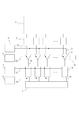
図1は、第1の実施形態の撮像装置を説明するためのブロック図である。撮像装置は、画素部1と、複数の読み出し部2と、複数の比較器3と、複数の記憶部4と、水平走査部5と、ランプ源6と、カウンタ7と、信号処理部8と、制御信号生成部9とを有する。そして、撮像装置は、制御信号生成部9が信号を出力する信号線52に接続する信号線制御部10を有する。この信号線制御部については、後に詳述する。また、撮像装置は、垂直走査部等の機能ブロック(不図示)を更に有している。
FIG. 1 is a block diagram for explaining the imaging apparatus according to the first embodiment. The imaging apparatus includes a pixel unit 1, a plurality of
画素部1には、複数の画素が行列状に配置されている。読み出し部2は、画素部1の画素列に対応して配置され、画素部1からの画素信号を信号線13へ出力する。ランプ源6は、ランプ信号用の信号線11を介して、ランプ信号を複数の比較器3に供給する。ランプ信号は参照信号とも称する。ランプ信号は、一般には、時間に応じて単調に増加あるいは減少する信号であるが、例えば、階段状に変化する信号であってもよい。カウンタ7は、カウントデータ用の信号線12を介して、カウント値を複数の記録部4に供給する。
A plurality of pixels are arranged in a matrix in the pixel unit 1. The
比較器3は、画素部1の画素列に対応して配置される。比較器3は、画素信号とランプ信号とを比較し、比較結果に応じたHレベル、又はLレベルの信号を信号線15へ出力する。比較器3が出力する信号は、画素信号の電位とランプ信号の電位の大小関係が変わる際に、HレベルからLレベル、又はLレベルからHレベルへと遷移(反転)する。記憶部4は、比較器3が出力した信号が反転するタイミングで、カウント値をデジタルデータとして記憶する。この動作によって、画素信号がデジタルデータに変換(AD変換)される。ここで、比較器3には、制御信号生成部9から、信号線52を介して、比較器3の動作を制御するための制御信号が供給されている。AD変換部は、少なくとも比較器3と、記憶部4を含む。本実施形態のAD変換器は、いわゆるランプ型AD変換器である。
The
水平走査部5は、記憶部4の信号の出力を制御する制御信号を信号線16へ出力する。記憶部4に記憶されたデジタルデータは、水平走査部5の制御信号によって、信号線14に出力され、信号処理部8へ順次転送される。信号処理部8では、デジタルデータを用いて相関二重サンプリング(以下、CDS)などの信号処理を行った後、撮像装置の外部へ信号を出力する。
The
本実施形態では、1つの画素列に対して、1つの読み出し部2と、1つの比較器3が設けられているが、複数の画素列に対して1つの読み出し部2や1つの比較器3が設けられていてもよい。また、撮像装置は、読み出し部2を有していない構成であってもよい。
In this embodiment, one
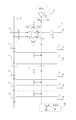
図2は、複数の比較器3の構成を示した回路図である。図2では1つの比較器3の回路構成を示しているが、他の比較器3も同一の構成を有しているものとする。図2は、図1のブロック図を左に90度回転させた図となっている。複数の比較器3のそれぞれは、差動増幅回路21と、出力回路22と、入力用の2つの容量を有する。差動増幅回路21は、帰還(フィードバック、以下FB)経路の形成を制御するFBスイッチを有する。各比較器3のFBスイッチには、共通の信号線52から、制御信号PFBが供給されている。制御信号生成部9は、バッファ51を含む。元となる信号iPFBが入力されたバッファ51は、信号線52に制御信号PFBを出力する。
FIG. 2 is a circuit diagram showing the configuration of the plurality of
ここで、図1にも示したように、撮像装置は、信号線52に接続する信号線制御部10を有する。信号線制御部10は、信号線52の電位を固定電位に制御するための回路を含み、信号線52の電位を固定電位にする、あるいは近づけるように動作する。本実施形態では、信号線制御部10は、固定電位としてグランド電位を供給する電源GNDと、スイッチ53を含む。スイッチ53は制御信号PFXによって、そのオンオフが制御されている。制御信号PFXによってスイッチ53がオフの場合には、信号線制御部10は動作せず、制御信号PFXによってスイッチ53がオンの場合には、信号線制御部10は動作する。このような構成によって、信号線52の電位は、制御信号生成部9と信号線制御部10によって、一定の電位になるように制御される。よって、ある比較器3の出力が反転した場合に、反転による変動が信号線52を介して別の比較器3へ伝搬することを低減することが可能となる。
Here, as illustrated in FIG. 1, the imaging apparatus includes the signal
以下、本実施形態についてより詳細に説明する。図3(a)及び図3(b)は、図2に示す比較器3を詳細に示した回路図である。図3(b)は、図3(a)の差動増幅回路21をより詳細に記載した回路図である。
Hereinafter, this embodiment will be described in more detail. FIGS. 3A and 3B are circuit diagrams showing in detail the
図3(a)に示すように、比較器3は、差動増幅回路21と、出力回路22と、入力用の2つの容量24、25を有する。差動増幅回路21は、非反転入力端子ipと、反転入力端子inと、非反転出力端子opと、反転出力端子onと、2つのFBスイッチ23とを有する。1つのFBスイッチ23は、一端が反転入力端子inと接続し、他端が非反転出力端子opと接続し、反転入力端子inと非反転出力端子opとの接続を制御する。もう1つのFBスイッチ23は、一端が非反転入力端子ipと接続し、他端が反転出力端子onと接続し、非反転入力端子ipと反転出力端子onとの接続を制御する。なお、差動増幅回路21の出力は、非反転出力端子opであり、この端子opが出力回路22の入力端子に接続される。反転入力端子inには容量24が接続され、非反転入力端子ipには容量25が接続される。反転入力端子inは、容量24を介して信号線13が接続され、非反転入力端子ipは、容量25を介して信号線11に接続される。信号線11は、ランプ信号が供給されている。出力回路22は、ソース接地増幅回路である。出力回路22の出力端子が信号線15に接続しており、出力回路22が出力する信号は比較器3が出力する信号となる。
As shown in FIG. 3A, the
図3(b)は差動増幅回路21の詳細を示した回路図である。差動増幅回路21は、差動入力トランジスタ対と、電流源26と、カレントミラー回路28とを含む。差動入力トランジスタ対は、P型のMOSトランジスタであるトランジスタM1、M2である。電流源26は、例えば定電流源であり、トランジスタM1、M2のソースに接続される。カレントミラー回路28は、ドレインとゲートがダイオード接続されたトランジスタM3と、ゲートがM3のゲートと接続されたトランジスタM4と、例えばグランド電位の電源GNDからなる。
FIG. 3B is a circuit diagram showing details of the
2つのFBスイッチ23は、N型MOSトランジスタからなる。1つのFBスイッチ23がトランジスタM1のゲートとドレインの間を接続し、もう1つのFBスイッチ23がトランジスタM2のゲートとドレインとの間を接続する。トランジスタM1のゲートが非反転入力端子ipであり、容量25を介して信号線11に接続される。トランジスタM1のドレインが反転出力端子onであり、ダイオード接続されたトランジスタM3のドレインと接続される。また、トランジスタM2のゲートが反転入力端子inであり、容量24を介して、信号線13が接続される。またM2のドレインが非反転出力端子opであり、ダイオード接続されたトランジスタM4のドレインと接続される。ここで、図2と図3(b)に示す容量Cfiは、信号線52と反転入力端子inとの間に生じる寄生容量である。図2と図3(b)に示す容量Cfoは、信号線52と非反転出力端子opとの間に生じる寄生容量である。
The two FB switches 23 are N-type MOS transistors. One
図4は、画素部1の1つの画素PIXと、1つの読み出し部2の回路を示した図である。画素PIXは、典型的なCMOSイメージセンサの回路であり、光電変換素子32と、リセットトランジスタ34と、転送トランジスタ35と、増幅トランジスタ36と、選択トランジスタ37と、を有する。リセットトランジスタ34と、転送トランジスタ35と、増幅トランジスタ36は、フローティングディフュージョン(以下、FD)のノードに接続されている。リセットトランジスタ34と、転送トランジスタ35と、選択トランジスタ37は、それぞれ制御信号PRES、PTX、PSELによって制御される。画素信号を読み出す時には、制御信号PSELがHレベルとなり、選択トランジスタ37がオンとなる。この時、増幅トランジスタ36と読み出し回路部2に含まれる電流源33とでソースフォロワ回路が形成される。読み出し部2は、画素信号が出力される信号線31に接続され、電流源33と、−A倍のゲインを持つアンプ38とで構成される。
FIG. 4 is a diagram illustrating a circuit of one pixel PIX of the pixel unit 1 and one
画素PIXから画素信号を読み出す際の動作は次のようになる。制御信号PRESがHレベルとなりリセットトランジスタ34がオンし、リセットトランジスタ34がFDをリセットする。そして、制御信号PRESがLレベルになりリセットトランジスタ34がオフする。ここで、選択トランジスタ37をオンの状態にしておくことで、リセットされたFDの電位に基づく信号(リセット信号)が信号線31に出力される。その後、制御信号PTXがHレベルになり、光電変換素子32に蓄えられた電荷がFDに転送される。この時、光電変換素子32において生じた電荷によってFDの電位が変化する。この変化したFDの電位に基づく信号(画像信号)が、信号線31に出力される。アンプ38では、リセット信号と画像信号をそれぞれ−A倍し、出力する。画素から出力されるリセット信号と画像信号を画素信号と称する。
The operation when reading out a pixel signal from the pixel PIX is as follows. The control signal PRES becomes H level, the
このような回路構成の本実施形態の撮像装置の動作について、図5を用いて説明する。図5は、画素PIXから比較器3までの動作を説明するためのタイミング図である。図5には、制御信号PTXと、制御信号PFBと、制御信号PFXと、信号線31の電位V31と、信号線13の電位V13と、ランプ信号の電位Vrampが示されている。更に、図5には、差動増幅回路21の非反転入力端子ipの電位Vip(実線)と、差動増幅回路21の反転入力端子inの電位Vin(点線)と、差動増幅回路21の非反転出力端子opの電位Vopが示されている。また、画素PIXの他の制御信号PSELや制御信号PRES、及び比較器3の出力については説明を簡易にするため省略する。
The operation of the imaging apparatus of this embodiment having such a circuit configuration will be described with reference to FIG. FIG. 5 is a timing chart for explaining the operation from the pixel PIX to the
時刻t1において、画素PIXからリセット信号が出力されており、電位V13は、リセット信号を示す電位Vnとなる。この時、制御信号PFXがLレベルに遷移する。ランプ信号の電位Vrampは、オフセットキャンセル用の電位Vclmpである。また、電位Vopは、電位Vclmp+電位Vofsである。電位Vofsとは、差動増幅回路21のオフセット電位である。
At time t1, a reset signal is output from the pixel PIX, and the potential V13 becomes a potential Vn indicating the reset signal. At this time, the control signal PFX changes to the L level. The potential Vramp of the ramp signal is the offset canceling potential Vclmp. Further, the potential Vop is the potential Vclmp + the potential Vofs. The potential Vofs is an offset potential of the
時刻t2において、制御信号PFBがHレベルに遷移する。つまり、FBスイッチ23がオンとなり、トランジスタM1のゲートの電位は、トランジスタM3のゲート電位である電位Vgsとなる。トランジスタM3のゲートの電位は、ソースがグランド電位であるため、ゲートとソース間の電圧Vgsと等しい(図3(b)参照)。この時、トランジスタM4のドレインとソース間に流れる電流と、トランジスタM3のドレインとソース間に流れる電流は等しい。よって、トランジスタM4のドレインと、それと同一ノードのトランジスタM2のゲートの電位も電位Vgsとなる。つまり、電位Vinと電位Vopが電位Vgsを示す。ここで、容量24の両端の電位差と容量25の両端の電位差は、電位Vclmp−電位Vgsである。
At time t2, the control signal PFB transitions to the H level. That is, the
時刻t3において、制御信号PFBはLレベルに遷移する。つまり、FBスイッチ23がオフとなり、容量24と容量25のそれぞれに、電位Vclmp−電位Vgsの差が保持される。この動作により、比較器3を構成する差動増幅回路21において、オフセットキャンセルを行うことができる。
At time t3, the control signal PFB transitions to the L level. That is, the
時刻t4において、制御信号PFXがHレベルに遷移し、時刻t5において、ランプ信号の電位Vrampが電位Vstに下がる。時刻t6において、電位Vrampが上昇し始め、AD変換が開始される。電位Vipは、ランプ信号の変化に伴って、時刻t5において電位が下がり、時刻t6において電位が上昇する。一方、電位Vopは、時刻t5から電位Vgsのままである。そして、時刻t7において、電位Vipが電位Vgsを超え、電位VopがLレベルからHレベルへ遷移する。つまり、比較器3の出力は、HレベルからLレベルになる。記憶部4は、この時のカウント値をリセット信号のデジタルデータとして記憶する。時刻t8において、ランプ信号の電位Vrampが再度、電位Vstに下がる。ここまででノイズ信号のAD変換が完了する。
At time t4, the control signal PFX changes to the H level, and at time t5, the potential Vramp of the ramp signal falls to the potential Vst. At time t6, the potential Vramp starts to rise and AD conversion is started. The potential Vip decreases at time t5 and increases at time t6 with the change of the ramp signal. On the other hand, the potential Vop remains at the potential Vgs from time t5. At time t7, the potential Vip exceeds the potential Vgs, and the potential Vop changes from the L level to the H level. That is, the output of the
次に、時刻t9において、制御信号PTXがLレベルからHレベルに遷移すると、画素PIXから画像信号が出力される期間になる。電位V13は、画像信号を示す電位Vsとなる。この時、電位Vinは電位Vgs+電位Vs−電位Vnとなる。時刻t10において、電位Vrampが上昇し始め、画像信号のAD変換が始まる。ここで、制御信号PTXは、例えば、時刻t11において、Lレベルに戻る。時刻t12において、電位Vipが電位Vgs+電位Vs−電位Vnを超えると、電位VopはLレベルからHレベルと遷移する。つまり、比較器3の出力は、HレベルからLレベルになる。記憶部4は、この時のカウント値を画像信号のデジタルデータとして記憶する。その後、時刻t13において、ランプ信号の電位の電位Vrampが再度、電位Vstに下がる。ここまでで画像信号のAD変換が完了する。その後、信号処理部8では、記憶部4に記憶されたリセット信号及び画像信号のデジタルデータの減算を行い出力し、1画素のAD変換が終了する。
Next, when the control signal PTX transitions from the L level to the H level at time t9, it is a period in which an image signal is output from the pixel PIX. The potential V13 is a potential Vs indicating an image signal. At this time, the potential Vin becomes the potential Vgs + the potential Vs−the potential Vn. At time t10, the potential Vramp starts to rise and AD conversion of the image signal starts. Here, for example, the control signal PTX returns to the L level at time t11. At time t12, when the potential Vip exceeds the potential Vgs + potential Vs−potential Vn, the potential Vop changes from the L level to the H level. That is, the output of the
本実施形態においては、制御信号PFBがLレベルからHレベルに遷移する前に、制御信号PFXがHレベルからLレベルに遷移し、制御信号PFBがHレベルからLレベルに遷移した後に制御信号PFXがLレベルからHレベルに遷移する。つまり、制御信号PFBがHレベルであるオフセットキャンセル期間には、信号線制御部10が動作しない。また、リセット信号と画素信号のAD変換期間(時刻t6〜時刻t8と時刻t10〜時刻t13)は、信号線制御部10が動作し、信号線52の電位が固定電位になるように制御している。この動作によって、他の比較器3へのクロストークを低減することができ、AD変換の誤差を低減することが可能となる。
In the present embodiment, the control signal PFX transitions from the H level to the L level before the control signal PFB transitions from the L level to the H level, and the control signal PFX transitions after the control signal PFB transitions from the H level to the L level. Transition from L level to H level. That is, the signal
図6〜図9を用いて、このクロストークの現象について説明する。まず、本実施形態の比較例について図7〜図9を用いて説明する。 The crosstalk phenomenon will be described with reference to FIGS. First, a comparative example of the present embodiment will be described with reference to FIGS.
図7は、本実施形態の比較例の撮像装置の複数の比較器3を示す回路図である。図7は、図2と対応しており、図2で説明した個所については詳細な説明は省略する。図7が図2と異なる点は、撮像装置に信号線制御部10が設けられていない点である。
FIG. 7 is a circuit diagram showing a plurality of
図8は、画素部1に光が入射されていない時、すなわち暗時のリセット信号と画像信号のAD変換期間を示したタイミング図である。図8は、比較器3の差動増幅回路21の各端子の電位と、信号線52の電位V52を示している。差動増幅回路21の各端子の電位として、非反転入力端子ipの電位Vipと、反転入力端子inの電位Vinと、非反転出力端子opの電位Vopを示す。図8では、第1〜第6の画素列に対応して設けられた複数の比較器3の各電位を示している。複数の比較器3を第1〜第6の比較器3とする。第1〜第6の比較器3の電位Vinを、電位Vin1〜電位Vin6と示す。一方、第1〜第6の比較器3の電位Vipは、説明を簡単にするためにばらつきがないものとし、1つの電位Vipとして示す。第1〜第6の比較器3の電位Vopを、電位Vop1〜電位Vop6として示す。なお、図8において電位Vop4と電位Vop5は省略されている。
FIG. 8 is a timing chart showing an AD conversion period of a reset signal and an image signal when light is not incident on the pixel unit 1, that is, when dark. FIG. 8 shows the potential of each terminal of the
時刻t1において、リセット信号のAD変換が始まる。このAD変換の開始時のカウント値は0である。時刻t2において、第1の画素列の電位Vin1と電位Vipの大小関係が変わり、電位Vop1がLレベルからHレベルへ遷移する。この電位Vop1のプラス(以下、+)方向への遷移は、図7に示した非反転出力端子opと信号線52との間の寄生容量Cfoを介して、信号線52の電位V52を+方向に変動させる。しかし、制御信号生成部9によって、信号線52がLレベルに制御されているため、信号線52はある時間を経ると元の電位となる。結果として、信号線52の電位V52は上凸状の波形となる。この時、信号線52の変動は、FBスイッチ23の周りにおける寄生容量Cfo、Cfiが主な要因であると考えられる。しかし、信号線52の変動は、出力端子opに接続する配線等と信号線52との間の寄生容量や入力端子inに接続する配線等と信号線52との間の寄生容量でも生じる可能性がある。
At time t1, AD conversion of the reset signal starts. The count value at the start of this AD conversion is zero. At time t2, the magnitude relationship between the potential Vin1 and the potential Vip of the first pixel column changes, and the potential Vop1 changes from the L level to the H level. The transition of the potential Vop1 in the plus (hereinafter “+”) direction causes the potential V52 of the
時刻t3において、第2の画素列の電位Vin2と電位Vipの大小関係が変わり、時刻t4において、第3の画素列の電位Vin3と電位Vipの大小関係が変わる。よって、対応する電位Vop2と電位Vop3は、それぞれの時刻において、LレベルからHレベルに遷移する。この電位Vop2と電位Vop3の+方向への遷移も、電位V52を+方向に変動させる。時刻t3に生じる電位V52の変動は電位Vop1の変動に重畳し、時刻t4に生じる変動は時刻t3に生じる電位V52の変動に重畳する。電位Vin4及び電位Vin5に対応する電位Vop4及び電位Vop5も同様に、電位V52を変動させる。つまり、電位V52が変動した後、元の電位に戻る前に、他の画素列の電位VopがLレベルからHレベルに遷移すると、電位V52の変動は大きくなってしまう。また、同時刻に電位VopがLレベルからHレベルに遷移する画素列が多いほど、電位V52の変動は大きくなってしまう。 At time t3, the magnitude relationship between the potential Vin2 and the potential Vip of the second pixel column changes, and at time t4, the magnitude relationship between the potential Vin3 and the potential Vip of the third pixel column changes. Therefore, the corresponding potential Vop2 and potential Vop3 transition from the L level to the H level at the respective times. The transition of the potential Vop2 and the potential Vop3 in the + direction also changes the potential V52 in the + direction. The fluctuation of the potential V52 that occurs at time t3 is superimposed on the fluctuation of the potential Vop1, and the fluctuation that occurs at time t4 is superimposed on the fluctuation of the potential V52 that occurs at time t3. Similarly, the potential Vop4 and the potential Vop5 corresponding to the potential Vin4 and the potential Vin5 also change the potential V52. That is, if the potential Vop of another pixel column transitions from the L level to the H level before the potential V52 changes and then returns to the original potential, the variation in the potential V52 increases. In addition, as the number of pixel columns in which the potential Vop changes from the L level to the H level at the same time, the variation in the potential V52 increases.
ここで、電位V52の変動は、図7に示した信号線52と反転入力端子inとの間の寄生容量Cfiを介して、反転入力端子inの電位Vinを変動させる。この変動を、図8の時刻t2〜時刻t7の間の電位Vin6に示している。なお、比較のために電位Vin6においてクロストークの影響がない状態を点線で示す。電位Vin6は、電位Vin0〜電位Vin5の電位よりも大きいため、電位Vin6と電位Vipの電位の大小関係が変わる前に、電位Vop1〜電位Vop5が遷移してしまう。この電位Vop1〜電位Vop5の遷移による変動が、電位Vin6の値に影響を与えてしまう。
Here, the variation of the potential V52 varies the potential Vin of the inverting input terminal in via the parasitic capacitance Cfi between the
時刻t6において、電位Vin6と電位ipとの大小関係が変わり、電位Vop6はLレベルからHレベルへ遷移する。この時刻t6のカウント値が記憶部4に保持される。しかし、クロストークの影響がなければ、時刻t5において電位Vop6の遷移が生じたはずである。つまり、信号線52の変動によって、時刻t5−時刻t6分のカウントだけデジタルデータに誤差が生じてしまう。
At time t6, the magnitude relationship between the potential Vin6 and the potential ip changes, and the potential Vop6 transitions from the L level to the H level. The count value at time t6 is held in the storage unit 4. However, if there is no influence of crosstalk, the transition of the potential Vop6 should have occurred at time t5. That is, due to the fluctuation of the
時刻t7において、電位VipがAD変換の開始前の電位に戻り、カウンタもリセットされカウント値が0になる。そして、時刻t8から、画像信号のAD変換が始まる。なお、暗時の画像信号であるため、電位Vin1〜電位Vin6は、リセット信号の電位Vin1〜電位Vin6とほぼ同じ値である。よって、時刻t9〜時刻t11は、時刻t2〜時刻t4と同様の動作が行われる。つまり、順次、電位Vin1〜電位Vin3と電位ipとの大小関係の変化が生じ、電位Vop1〜電位Vop3のLレベルからHレベルへの遷移が生じる。電位Vin4及び電位Vin5に対応する電位Vop4及び電位Vop5も同様に遷移する。よって、電位V52に変動の影響が生じ、電位Vin6に変動が生じる。この変動によって、電位Vop6がLレベルからHレベルに遷移する時刻は、時刻t12ではなく時刻t13となる。 At time t7, the potential Vip returns to the potential before the start of AD conversion, the counter is reset, and the count value becomes zero. Then, from time t8, AD conversion of the image signal starts. Since the image signal is dark, the potentials Vin1 to Vin6 have substantially the same values as the potentials Vin1 to Vin6 of the reset signal. Therefore, from time t9 to time t11, the same operation as time t2 to time t4 is performed. That is, the magnitude relationship between the potentials Vin1 to Vin3 and the potential ip changes sequentially, and the potentials Vop1 to Vop3 change from the L level to the H level. Similarly, the potential Vop4 and the potential Vop5 corresponding to the potential Vin4 and the potential Vin5 transit. Therefore, the potential V52 is affected by the fluctuation, and the potential Vin6 is fluctuated. Due to this variation, the time when the potential Vop6 transitions from the L level to the H level is not the time t12 but the time t13.
ここで、暗時の撮影で、電位Vin1〜電位Vin6のリセット信号の値と撮像信号の値で大きな違いがなければ、電位Vin6のリセット信号と撮像信号に生じる変動がほぼ等しくなる可能性がある。この場合には、画像信号のデジタルデータからリセット信号のデジタルデータを減算するCDS処理を行えば、誤差を無くす、あるいは低減することができる。しかし、撮像装置を用いる場合には、多くの場合において、リセット信号の値と撮像信号の値が異なるため、誤差を低減することは困難である。また、暗時であっても、欠陥画素等が存在すると、誤差が生じる可能性がある。 Here, if there is no significant difference between the reset signal value of the potential Vin1 to the potential Vin6 and the value of the imaging signal in dark imaging, there is a possibility that the fluctuations generated in the reset signal of the potential Vin6 and the imaging signal are almost equal. . In this case, the error can be eliminated or reduced by performing CDS processing for subtracting the digital data of the reset signal from the digital data of the image signal. However, when an imaging device is used, it is difficult to reduce the error because the value of the reset signal is different from the value of the imaging signal in many cases. Even in the dark, if there are defective pixels or the like, an error may occur.
更に、図9を用いて、画素部1に光が入射されている場合について説明する。図9は、画素部1に光が入射されている場合のリセット信号と画像信号のAD変換期間を示したタイミング図である。図9は図8と対応しており、同一の符号を付したものの説明は省略する。時刻t1〜時刻t7は、図8の時刻t1〜時刻t7と同じ動作が行われているため説明を省略する。 Further, a case where light is incident on the pixel portion 1 will be described with reference to FIG. FIG. 9 is a timing chart showing the AD conversion period of the reset signal and the image signal when light is incident on the pixel unit 1. FIG. 9 corresponds to FIG. 8, and the description of the same reference numerals is omitted. From time t1 to time t7, the same operation as time t1 to time t7 in FIG.
時刻t8において、画素PIXから画像信号が出力され、電位Vin1〜電位Vin6の電位が変化する。ここでは、第1〜第6の画素列のうち、第1、3、5の画素列に光が入射されたものとする。 At time t8, an image signal is output from the pixel PIX, and the potentials Vin1 to Vin6 change. Here, it is assumed that light is incident on the first, third, and fifth pixel columns among the first to sixth pixel columns.
時刻t9において、画像信号のAD変換が開示される。時刻t10にて、電位Vin2と電位Vipの大小関係が変わり、電位Vop2がLレベルからHレベルへ遷移する。この時、電位V52が電位Vop2の遷移に伴って変動する。その後、電位Vin4と電位Vipの大小関係が変わり、電位Vop4がLレベルからHレベルへ遷移する(不図示)。この時、電位V52には、電位Vop2の遷移に伴う変動に加え、電位Vop4の遷移に伴う変動が生じる。この時、信号線52を介して、電位Vin6の電位が変動してしまう。
At time t9, AD conversion of the image signal is disclosed. At time t10, the magnitude relationship between the potential Vin2 and the potential Vip changes, and the potential Vop2 changes from the L level to the H level. At this time, the potential V52 varies with the transition of the potential Vop2. Thereafter, the magnitude relationship between the potential Vin4 and the potential Vip changes, and the potential Vop4 changes from the L level to the H level (not shown). At this time, in addition to the fluctuation accompanying the transition of the potential Vop2, the fluctuation accompanying the transition of the potential Vop4 occurs in the potential V52. At this time, the potential Vin6 varies via the
そして、時刻t12において、電位Vin6と電位Vipの大小関係が変わり、電位Vop6がLレベルからHレベルへ遷移する。図8と同様に、変動がなければ、電位Vin6と電位Vipの大小関係の変化は時刻t11にて生じたはずである。 At time t12, the magnitude relationship between the potential Vin6 and the potential Vip changes, and the potential Vop6 changes from the L level to the H level. As in FIG. 8, if there is no change, the change in the magnitude relationship between the potential Vin6 and the potential Vip should have occurred at time t11.
その後、時刻t13において、電位Vin1と電位Vipの大小関係が変わり、電位Vop1がLレベルからHレベルへ遷移する。時刻t14において、電位Vin3と電位Vipの大小関係が変わり、電位Vop3がLレベルからHレベルへ遷移する。時刻t15において、電位Vin5と電位Vipの大小関係が変わり、電位Vop5がLレベルからHレベルへ遷移する(不図示)。時刻t13〜時刻t15においても、電位V52が電位Vop1や電位Vop3の遷移に伴って変動するため、電位Vin5が変動し、電位Vin5と電位Vipの大小関係が変わる時刻が変化してしまう可能性がある。 After that, at time t13, the magnitude relationship between the potential Vin1 and the potential Vip changes, and the potential Vop1 changes from the L level to the H level. At time t14, the magnitude relationship between the potential Vin3 and the potential Vip changes, and the potential Vop3 changes from the L level to the H level. At time t15, the magnitude relationship between the potential Vin5 and the potential Vip changes, and the potential Vop5 changes from the L level to the H level (not shown). Also from time t13 to time t15, since the potential V52 varies with the transition of the potential Vop1 and the potential Vop3, the potential Vin5 varies, and the time at which the magnitude relationship between the potential Vin5 and the potential Vip changes may change. is there.
図9の動作においては、リセット信号のAD変換の期間において、電位Vin6は、電位Vop1〜電位Vop5が遷移する影響を受ける。一方、画像信号のAD変換の期間においては、電位Vin6は、電位Vop2と電位Vop4が遷移する影響を受ける。つまり、電位Vin6が受ける変動の影響が、リセット信号のAD変換期間中と、画像信号のAD変換期間中とで異なる。よって、例えCDS処理を行ったとしても、誤差を無くすことができない。 In the operation of FIG. 9, during the AD conversion period of the reset signal, the potential Vin6 is affected by the transition of the potential Vop1 to the potential Vop5. On the other hand, during the AD conversion period of the image signal, the potential Vin6 is affected by the transition between the potential Vop2 and the potential Vop4. That is, the influence of the fluctuation that the potential Vin6 receives is different between the AD conversion period of the reset signal and the AD conversion period of the image signal. Therefore, even if the CDS process is performed, the error cannot be eliminated.
図8及び図9に示すように、比較器の出力が反転した際に、他の列の比較器の出力へと影響が生じてしまう場合がある。つまり、クロストークが生じてしまう。クロストークが生じると、他の列のAD変換の結果に誤差を生じさせてしまう。次に、図6を用いて、図1〜図5にて示した本実施形態の撮像装置によるクロストークの低減について説明する。 As shown in FIGS. 8 and 9, when the output of the comparator is inverted, the output of the comparator in the other column may be affected. That is, crosstalk occurs. When crosstalk occurs, an error is caused in the result of AD conversion of another column. Next, the reduction in crosstalk by the imaging apparatus according to the present embodiment shown in FIGS. 1 to 5 will be described with reference to FIG.
図6は、画素部1に光が入射されている場合のリセット信号と画像信号のAD変換期間を示したタイミング図である。図6は、図9と対応しており、同一の構成については説明を省略する。 FIG. 6 is a timing diagram illustrating an AD conversion period of the reset signal and the image signal when light is incident on the pixel unit 1. FIG. 6 corresponds to FIG. 9, and the description of the same configuration is omitted.
図6の時刻t1〜時刻t7は、ノイズ信号のAD変換期間であり、図9の時刻t1〜時刻t7と同様の動作が行われている。しかし、時刻t2から生じる電位V52の変動の量が、図9における電位V52の変動の量より小さい。そして、電位V52の変動に伴い生じる電位Vin6の変動の量も、図9における電位Vin6の変動の量より小さい。図1等に示すように、信号線制御部10によって、信号線52の電位V52が制御されているためである。よって、誤差である時刻t5−時刻t6分のカウントが、図9の時刻t5−時刻t6分のカウントよりも小さくなる。
Time t1 to time t7 in FIG. 6 is an AD conversion period of the noise signal, and operations similar to those from time t1 to time t7 in FIG. 9 are performed. However, the amount of variation in potential V52 that occurs from time t2 is smaller than the amount of variation in potential V52 in FIG. Further, the amount of fluctuation of the potential Vin6 caused by the fluctuation of the potential V52 is also smaller than the amount of fluctuation of the potential Vin6 in FIG. This is because the potential V52 of the
図6の時刻t8〜時刻t15は、画像信号の出力と、画像信号のAD変換期間であり、図9の時刻t7〜時刻t15と同様の動作が行われている。ノイズ信号のAD変換期間と同様に、時刻t10から生じる電位V52の変動の量が、図9における電位V52の変動の量より小さい。そして、電位V52の変動に伴い生じる電位Vin6の変動の量も、図9における電位Vin6の変動の量より小さい。図1等に示すように、信号線制御部10によって、信号線52の電位V52が制御されているためである。よって、誤差である時刻t11−時刻t12分のカウントが、図9の時刻t11−時刻t12分のカウントよりも小さくなる。
6 are an output of an image signal and an AD conversion period of the image signal, and operations similar to those at time t7 to time t15 in FIG. 9 are performed. Similar to the AD conversion period of the noise signal, the amount of fluctuation of the potential V52 generated from time t10 is smaller than the amount of fluctuation of the potential V52 in FIG. Further, the amount of fluctuation of the potential Vin6 caused by the fluctuation of the potential V52 is also smaller than the amount of fluctuation of the potential Vin6 in FIG. This is because the potential V52 of the
このように、クロストークを軽減することが可能となり、誤差が小さいノイズ信号と画像信号のデジタルデータを得ることができる。更に、CDS処理をすれば誤差を無くす、あるいはより低減することができる。 In this manner, crosstalk can be reduced, and digital data of a noise signal and an image signal with a small error can be obtained. Further, if the CDS process is performed, errors can be eliminated or further reduced.
本実施形態では、第6の画素列の画素信号のAD変換時に誤差が生じる場合について説明したが、他の画素列でも生じ得る。しかし、信号線制御部10を設けることで、他の画素列でのAD変換時の誤差も低減可能である。
In the present embodiment, the case where an error occurs during AD conversion of the pixel signal of the sixth pixel column has been described, but the error may occur in other pixel columns. However, by providing the signal
本実施形態では、図2に示すように信号線制御部10は、信号線制御部10と制御信号生成部9の間に複数の比較器3が位置するように配置されている。つまり、信号線52の一端に制御信号生成部9が接続し、信号線52の他端に信号線制御部10が接続している。しかし、信号線制御部10は、複数の比較器3の間に位置するように配置されていてもよい。また、信号線制御部10の数は1つに限らない。
In the present embodiment, as shown in FIG. 2, the signal
また、信号線制御部10は、図2に示す制御信号生成部9と同様の構成であってもよい。つまり、信号線52を両端から制御する構成であってもよい。しかしながら、このような構成では、信号線52に貫通電流が流れる可能性があるため、本実施形態の構成の方が好ましい。
Further, the signal
また、各比較器3の2つのFBスイッチ23は、同一の制御信号PFBで制御されている。しかし、例えば、2つのFBスイッチ23はそれぞれ別の制御信号によって、別に制御されていてもよい。この場合には、制御信号のための信号線のそれぞれに信号線制御部10を設けることが望ましい。
Further, the two FB switches 23 of each
更に、本実施形態の信号線制御部10のスイッチ53は電源GNDと接続しているが、電源GNDではなく電源電圧である電源VDDや、任意の電圧を供給する配線と接続していてもよい。
Furthermore, although the
なお、本実施形態では、動作を制御するためのスイッチとして、FBスイッチについて説明したが、他の比較器の動作を制御するスイッチであってもよい。この他の比較器の動作を制御するスイッチの例については、後述する。 In the present embodiment, the FB switch has been described as a switch for controlling the operation. However, a switch for controlling the operation of another comparator may be used. Examples of other switches that control the operation of the comparator will be described later.
本実施形態では、ランプ型AD変換器が有する比較器について説明したが、逐次比較型等のAD変換器でも、スイッチに対して共通に設けられた信号を有する構成であれば、信号線制御部10の構成は適用可能である。また、AD変換器だけでなく、信号を比較する場合、例えば、比較結果によって増幅器のゲインを切り替え、ダイナミックレンジを拡大させる等の機能を有する撮像装置においても、本実施形態で説明した信号線制御部10を比較器に適用することが可能である。
In the present embodiment, the comparator included in the ramp type AD converter has been described. However, if the AD converter such as the successive approximation type has a signal provided in common to the switch, the signal line control unit Ten configurations are applicable. In addition to the AD converter, when comparing signals, for example, the signal line control described in this embodiment also in an imaging apparatus having a function of switching the gain of the amplifier according to the comparison result and expanding the dynamic range. The
(第2の実施形態)
本実施形態について、図10を用いて説明する。図10において、第1の実施形態と同一の構成に対しては同一の符号を付し、説明を省略する。本実施形態では、第1の実施形態では1つであった信号線制御部10に対して、信号線制御部10に加えて別の信号線制御部20が設けられている。つまり、本実施形態では、複数の信号線制御部10、20が設けられている。
(Second Embodiment)
This embodiment will be described with reference to FIG. In FIG. 10, the same components as those of the first embodiment are denoted by the same reference numerals, and the description thereof is omitted. In the present embodiment, in addition to the signal
信号線制御部20は、第1の実施形態の信号線制御部10と同様に、電源GNDと、スイッチ100を有している。信号線制御部20は、制御信号生成部9と信号線制御部10との間に配置されている。制御信号生成部9と信号線制御部20との間と、信号線制御部10と信号線制御部20との間には、複数の比較器3が配置されている。このような構成によって、第1の実施形態よりも信号線52の変動を低減することが可能となり、AD変換時に生じる誤差を更に低減することが可能となる。
The signal
本実施形態では、撮像装置が2つの信号線制御部を有する構成を示したが、更に多くの信号線制御部を有していてもよい。複数の信号線制御部を設ける場合には、その配置は等間隔であることが望ましいが、それに限らない。 In the present embodiment, the configuration in which the imaging apparatus has two signal line control units has been described, but more image signal control units may be included. In the case where a plurality of signal line control units are provided, it is desirable that their arrangement be equally spaced, but this is not a limitation.
(第3の実施形態)
本実施形態について、図11を用いて説明する。図11において、第1の実施形態と同一の構成に対しては同一の符号を付し、説明を省略する。第1の実施形態の信号線制御部10は電源GNDとスイッチ53で構成されていたが、本実施形態では信号線制御部10はバッファ512で構成されている。
(Third embodiment)
This embodiment will be described with reference to FIG. In FIG. 11, the same components as those in the first embodiment are denoted by the same reference numerals, and description thereof is omitted. The signal
制御信号生成部9のバッファ51が制御信号PFBを信号線52に供給する。信号線52を介して信号線制御部10のバッファ512に制御信号PFBが入力され、バッファ512は制御信号PFBに基づく制御信号を信号線522へ出力する。つまり、1つのバッファが駆動する信号線の抵抗が小さくなるため、第1の実施形態に比べて、信号線52及び信号線522の変動を低減することが可能となる。よって、AD変換時に生じる誤差を更に低減することが可能となる。
The
なお、信号線522のバッファ512と接続する端部とは反対側の端部に、第1の実施形態の信号線制御部10を設けてもよい。これらの構成は、適宜、組み合わせることができる。
Note that the signal
(第4の実施形態)
本実施形態について、図12を用いて説明する。図12において、第1の実施形態と同一の構成に対しては同一の符号を付し、説明を省略する。第1の実施形態の比較器3の動作を制御するスイッチとして、FBスイッチ23の場合を説明したが、本実施形態では、電流源26のスイッチ610の場合を説明する。
(Fourth embodiment)
This embodiment will be described with reference to FIG. In FIG. 12, the same components as those of the first embodiment are denoted by the same reference numerals, and the description thereof is omitted. Although the case of the
図12は、第1の実施形態の図3(b)と対応する比較器3を詳細に示した回路図である。図12において、差動増幅回路21は、図3(b)の構成に加えて、電流源26と差動入力トランジスタ対との間の導通を制御するスイッチ610を有する。スイッチ610がオンする場合には、電流源26から電流が供給され差動増幅回路21が動作し、スイッチ610がオフする場合には、電流源26からの電流が供給されず差動増幅回路21が動作しない。よって、スイッチ610によって必要な時にだけ電流を流すことで、消費電力を低減することができる。このように、スイッチ610は比較器3の動作を制御する。
FIG. 12 is a circuit diagram showing in detail the
このスイッチ610の動作を制御する制御信号P610を供給する信号線611も、第1の実施形態の信号線52と同様に、複数の比較器3に共通に設けられる場合がある。このような場合においても、信号線611に信号線制御部を設けることで、他の比較器3へのクロストークを低減することが可能となる。よって、AD変換時の誤差を低減することが可能となる。
Similarly to the
また、図12は、出力回路22の回路の一例を示している。出力回路22は、ソース接地増幅回路であり、電源VDDと、電流源620と、トランジスタ621と、トランジスタ622と、電源GNDとを有する。トランジスタ621とトランジスタ622は例えば、N型のMOSトランジスタである。トランジスタ622は、差動増幅回路21の出力端子opと接続するゲートと、出力端子outを有するドレインと、電源GNDと接続したソースとを有する。トランジスタ621は、電流源620と、トランジスタ622のドレインとの間の導通を制御するスイッチである。トランジスタ621はゲートに供給される制御信号P621によって動作が制御されている。ここで、制御信号P621を供給する信号線623は、他の比較器3の出力回路22と共通に設けられる場合がある。このような場合においても、差動増幅回路21の出力端子opの電位の変動を他の比較器3に伝搬してしまう可能がある。よって、出力回路22の制御信号を供給する信号線623に対しても、信号線制御部を設けてもよい。
FIG. 12 shows an example of the
(第5の実施形態)
本実施形態について、図13を用いて説明する。図13は撮像システムの構成例を示すブロック図である。撮像システム800には、撮影を主目的とする装置(例えば、カメラ、カムコーダ)のみならず、撮影機能を補助的に備える装置(例えば、パーソナルコンピュータ、携帯端末)も含まれる。撮像システムは、上記の実施形態として例示された撮像装置と、該撮像装置から出力される信号を処理する処理部とを含む。該処理部は、例えば、撮像装置から出力されるデジタルデータを処理するプロセッサを含みうる。
(Fifth embodiment)
This embodiment will be described with reference to FIG. FIG. 13 is a block diagram illustrating a configuration example of the imaging system. The
図13において、撮像システム800は、例えば、光学部810、撮像装置820、映像信号処理部830、記録・通信部840、タイミング制御部850、システム制御部860、及び再生・表示部870を含む。
In FIG. 13, the
レンズ等の光学系である光学部810は、被写体からの光を撮像装置820の、複数の画素が2次元状に配列された画素部1に結像させ、被写体の像を形成する。撮像装置820は、タイミング制御部850からの信号に基づくタイミングで、画素部1に結像された光に応じた信号を出力する。撮像装置820から出力された信号は、処理部である映像信号処理部830に入力され、映像信号処理部830が、プログラム等によって定められた方法に従って信号処理を行う。映像信号処理部830での処理によって得られた信号は画像データとして記録・通信部840に送られる。記録・通信部840は、画像を形成するための信号を再生・表示部870に送り、再生・表示部870に動画や静止画像を再生・表示させる。記録・通信部840は、また、映像信号処理部830からの信号を受けて、システム制御部860と通信を行うほか、不図示の記録媒体に、画像を形成するための信号を記録する動作も行う。
An
システム制御部860は、撮像システムの動作を統括的に制御するものであり、光学部810、タイミング制御部850、記録・通信部840、及び再生・表示部870の駆動を制御する。また、システム制御部860は、例えば記録媒体である不図示の記憶装置を備え、ここに撮像システムの動作を制御するのに必要なプログラム等が記録される。また、システム制御部860は、例えばユーザの操作に応じて駆動モードを切り替える信号を撮像システム内に供給する。具体的な例としては、読み出す行やリセットする行の変更、電子ズームに伴う画角の変更や、電子防振に伴う画角のずらし等である。タイミング制御部850は、システム制御部860による制御に基づいて撮像装置820及び映像信号処理部830の駆動タイミングを制御する。また、タイミング制御部850は、撮像装置820の撮影感度を設定する感度設定部としても機能しうる。
The
上述の実施形態の撮像装置によって、AD変換時の誤差を低減することが可能となる。各実施形態の構成は、適宜変更することが可能である。また、各実施形態を適宜組み合わせることも可能である。 With the imaging device of the above-described embodiment, it is possible to reduce errors during AD conversion. The configuration of each embodiment can be changed as appropriate. Moreover, it is also possible to combine each embodiment suitably.
1 画素部
2 読み出し部
3 比較器
4 記憶部
6 ランプ源
7 カウンタ
9 制御信号生成部
10 信号線制御部
52 信号線
DESCRIPTION OF SYMBOLS 1
Claims (16)
それぞれが前記複数の画素の少なくとも1つの画素列に対応して設けられ、それぞれが動作を制御するためのスイッチを含む複数の比較器と、
前記複数の比較器の前記スイッチに対して共通に設けられ、前記複数の比較器の前記スイッチを制御する制御信号を供給するための信号線と、
前記信号線に前記制御信号を供給する制御信号生成部と、
を有する撮像装置において、
前記撮像装置は、前記信号線の電位を固定電位に制御するための信号線制御部をさらに有し、
前記制御信号生成部と、前記信号線制御部との間に、前記複数の比較器が配置されていることを特徴とする撮像装置。 A plurality of pixels arranged in a matrix;
A plurality of comparators each provided corresponding to at least one pixel column of the plurality of pixels, each including a switch for controlling operation;
A signal line provided in common to the switches of the plurality of comparators, for supplying a control signal for controlling the switches of the plurality of comparators;
A control signal generator for supplying the control signal to the signal line;
In an imaging apparatus having
The imaging apparatus further includes a signal line control unit for controlling the potential of the signal line to a fixed potential,
The imaging apparatus , wherein the plurality of comparators are arranged between the control signal generation unit and the signal line control unit .
前記複数の比較器のそれぞれにおいて、前記スイッチは、前記出力端子と一端が接続され、前記入力端子と前記出力端子との接続を制御することを特徴とする請求項1に記載の撮像装置。 Each of the plurality of comparators includes a differential amplifier circuit including an input terminal and an output terminal;
2. The imaging apparatus according to claim 1, wherein in each of the plurality of comparators, the switch is connected at one end to the output terminal and controls connection between the input terminal and the output terminal.
前記スイッチは、前記電流源のオンオフを制御することを特徴とする請求項1に記載の撮像装置。 Each of the plurality of comparators includes a differential amplifier circuit including a current source;
The imaging apparatus according to claim 1, wherein the switch controls on / off of the current source.
前記信号線は、第1の信号線と第2の信号線とを有し、
前記第1の信号線は前記バッファの前記入力端子と接続し、前記第2の信号線は前記バッファの前記出力端子と接続することを特徴とする請求項1乃至5のいずれか1項に記載の撮像装置。 The signal line control unit has a buffer including an input terminal and an output terminal,
The signal line has a first signal line and a second signal line,
The first signal line is connected to the input terminal of the buffer, and the second signal line is connected to the output terminal of the buffer. Imaging device.
前記信号線制御部は、前記信号線の他端と接続することを特徴とする請求項1乃至6のいずれか1項に記載の撮像装置。 The control signal generator is connected to one end of the signal line,
The imaging apparatus according to claim 1, wherein the signal line control unit is connected to the other end of the signal line.
前記複数の比較器のそれぞれの前記出力回路は、第2の出力端子と、前記第2の出力端子と接続する第2のスイッチを有し、
前記撮像装置は、前記複数の比較器の前記第2のスイッチを制御する第2の制御信号を前記制御信号生成部から供給され、前記複数の比較器の前記第2のスイッチに対して共通に設けられ、前記複数の比較器の前記第2のスイッチに前記第2の制御信号を供給する第2の信号線と、前記第2の信号線を固定電位に接続するための第3の信号線制御部と、を有することを特徴とする請求項1乃至11のいずれか1項に記載の撮像装置。 Each of the plurality of comparators includes a differential amplifier circuit and an output circuit for outputting a signal from the differential amplifier circuit,
Each of the output circuits of the plurality of comparators includes a second output terminal and a second switch connected to the second output terminal;
The imaging apparatus is supplied with a second control signal for controlling the second switch of the plurality of comparators from the control signal generation unit, and is common to the second switch of the plurality of comparators. A second signal line provided to supply the second control signal to the second switch of the plurality of comparators; and a third signal line for connecting the second signal line to a fixed potential The imaging apparatus according to claim 1, further comprising: a control unit.
前記複数の比較器と前記複数の記憶部がAD変換器を構成することを特徴とする請求項1乃至13のいずれか1項に記載の撮像装置。 Furthermore, each has a plurality of storage units for holding a count value based on signals from the plurality of comparators,
The imaging device according to any one of claims 1 to 13, wherein the plurality of comparators and the plurality of storage units constitute an AD converter.
前記撮像装置からの信号を処理する処理部と、を有する撮像システム。 The imaging device according to any one of claims 1 to 15,
And a processing unit that processes a signal from the imaging device.
Priority Applications (2)
| Application Number | Priority Date | Filing Date | Title |
|---|---|---|---|
| JP2014244334A JP6422319B2 (en) | 2014-12-02 | 2014-12-02 | Imaging apparatus and imaging system using the same |
| US14/954,830 US9800815B2 (en) | 2014-12-02 | 2015-11-30 | Image pickup apparatus and image pickup system using image pickup apparatus |
Applications Claiming Priority (1)
| Application Number | Priority Date | Filing Date | Title |
|---|---|---|---|
| JP2014244334A JP6422319B2 (en) | 2014-12-02 | 2014-12-02 | Imaging apparatus and imaging system using the same |
Publications (3)
| Publication Number | Publication Date |
|---|---|
| JP2016111402A JP2016111402A (en) | 2016-06-20 |
| JP2016111402A5 JP2016111402A5 (en) | 2018-01-18 |
| JP6422319B2 true JP6422319B2 (en) | 2018-11-14 |
Family
ID=56080002
Family Applications (1)
| Application Number | Title | Priority Date | Filing Date |
|---|---|---|---|
| JP2014244334A Active JP6422319B2 (en) | 2014-12-02 | 2014-12-02 | Imaging apparatus and imaging system using the same |
Country Status (2)
| Country | Link |
|---|---|
| US (1) | US9800815B2 (en) |
| JP (1) | JP6422319B2 (en) |
Families Citing this family (1)
| Publication number | Priority date | Publication date | Assignee | Title |
|---|---|---|---|---|
| JP6758952B2 (en) * | 2016-06-28 | 2020-09-23 | キヤノン株式会社 | Imaging equipment and imaging system |
Family Cites Families (6)
| Publication number | Priority date | Publication date | Assignee | Title |
|---|---|---|---|---|
| JP4418809B2 (en) * | 2006-08-30 | 2010-02-24 | キヤノン株式会社 | Solid-state imaging device and imaging system |
| JP4674589B2 (en) | 2007-02-05 | 2011-04-20 | ソニー株式会社 | Solid-state imaging device and imaging device |
| JP4900200B2 (en) * | 2007-11-15 | 2012-03-21 | ソニー株式会社 | Solid-state imaging device and camera system |
| JP4725608B2 (en) | 2008-07-03 | 2011-07-13 | ソニー株式会社 | Comparator, comparator calibration method, solid-state imaging device, and camera system |
| WO2014038140A1 (en) * | 2012-09-10 | 2014-03-13 | パナソニック株式会社 | Solid-state imaging device and imaging device |
| JP2014096670A (en) * | 2012-11-08 | 2014-05-22 | Sony Corp | Comparator, comparison method, ad converter, solid state image sensor, and electronic device |
-
2014
- 2014-12-02 JP JP2014244334A patent/JP6422319B2/en active Active
-
2015
- 2015-11-30 US US14/954,830 patent/US9800815B2/en active Active
Also Published As
| Publication number | Publication date |
|---|---|
| US20160156866A1 (en) | 2016-06-02 |
| US9800815B2 (en) | 2017-10-24 |
| JP2016111402A (en) | 2016-06-20 |
Similar Documents
| Publication | Publication Date | Title |
|---|---|---|
| JP6057931B2 (en) | Photoelectric conversion device and imaging system using the same | |
| JP6385192B2 (en) | Imaging apparatus, imaging system, and driving method of imaging system | |
| US20080303705A1 (en) | A/D conversion circuit, control method thereof, solid-state imaging device, and imaging apparatus | |
| JP6317568B2 (en) | Comparison circuit, image pickup device using the same, and control method of comparison circuit | |
| JP6708381B2 (en) | Photoelectric conversion device and photoelectric conversion system | |
| JP2016201649A (en) | Imaging apparatus, imaging system, and driving method for imaging apparatus | |
| JP6245882B2 (en) | Photoelectric conversion device and imaging system | |
| WO2013031097A1 (en) | Solid-state imaging device and imaging device | |
| JP2013058909A (en) | Solid-state imaging device | |
| JP2010016656A (en) | Comparator, method of calibrating comparator, solid-state imaging device, and camera system | |
| JP2016005054A (en) | Solid-state image pickup device | |
| JP6338440B2 (en) | Imaging device driving method, imaging device, and imaging system | |
| JP2005311487A (en) | Solid-state imaging unit and drive method of solid-state imaging unit | |
| US10044964B2 (en) | Column signal processing unit with driving method for photoelectric conversion apparatus, photoelectric conversion apparatus, and image pickup system | |
| JP2015213260A (en) | Solid state image pickup device and imaging system | |
| JP6053398B2 (en) | Imaging device driving method, imaging system driving method, imaging device, and imaging system | |
| US20160142661A1 (en) | Solid-state imaging device and camera | |
| US10811448B2 (en) | Solid-state imaging device | |
| JP2015095874A (en) | Solid state imaging device, imaging system, and method of driving solid state imaging device | |
| JP6422319B2 (en) | Imaging apparatus and imaging system using the same | |
| JP6385190B2 (en) | Photoelectric conversion device driving method, photoelectric conversion device, and imaging system | |
| JP2018019335A (en) | Image pick-up device and imaging apparatus | |
| JP6555979B2 (en) | Imaging apparatus and imaging system | |
| WO2015111370A1 (en) | Solid-state imaging device and imaging device |
Legal Events
| Date | Code | Title | Description |
|---|---|---|---|
| A521 | Request for written amendment filed |
Free format text: JAPANESE INTERMEDIATE CODE: A523 Effective date: 20171201 |
|
| A621 | Written request for application examination |
Free format text: JAPANESE INTERMEDIATE CODE: A621 Effective date: 20171201 |
|
| A977 | Report on retrieval |
Free format text: JAPANESE INTERMEDIATE CODE: A971007 Effective date: 20180910 |
|
| TRDD | Decision of grant or rejection written | ||
| A01 | Written decision to grant a patent or to grant a registration (utility model) |
Free format text: JAPANESE INTERMEDIATE CODE: A01 Effective date: 20180918 |
|
| A61 | First payment of annual fees (during grant procedure) |
Free format text: JAPANESE INTERMEDIATE CODE: A61 Effective date: 20181016 |
|
| R151 | Written notification of patent or utility model registration |
Ref document number: 6422319 Country of ref document: JP Free format text: JAPANESE INTERMEDIATE CODE: R151 |