JP4794877B2 - Solid-state imaging device and camera - Google Patents
Solid-state imaging device and camera Download PDFInfo
- Publication number
- JP4794877B2 JP4794877B2 JP2005080343A JP2005080343A JP4794877B2 JP 4794877 B2 JP4794877 B2 JP 4794877B2 JP 2005080343 A JP2005080343 A JP 2005080343A JP 2005080343 A JP2005080343 A JP 2005080343A JP 4794877 B2 JP4794877 B2 JP 4794877B2
- Authority
- JP
- Japan
- Prior art keywords
- mos transistor
- region
- solid
- imaging device
- state imaging
- Prior art date
- Legal status (The legal status is an assumption and is not a legal conclusion. Google has not performed a legal analysis and makes no representation as to the accuracy of the status listed.)
- Expired - Fee Related
Links
- 238000003384 imaging method Methods 0.000 title claims description 43
- 238000012546 transfer Methods 0.000 claims description 72
- 238000009792 diffusion process Methods 0.000 claims description 38
- 238000005036 potential barrier Methods 0.000 claims description 34
- 238000006243 chemical reaction Methods 0.000 claims description 10
- 239000012535 impurity Substances 0.000 claims description 10
- 239000004065 semiconductor Substances 0.000 claims description 10
- 238000009825 accumulation Methods 0.000 claims description 6
- 239000000758 substrate Substances 0.000 claims description 6
- 230000003287 optical effect Effects 0.000 claims description 3
- 239000003990 capacitor Substances 0.000 description 21
- 238000010586 diagram Methods 0.000 description 11
- 238000000034 method Methods 0.000 description 7
- 238000012545 processing Methods 0.000 description 6
- 238000004364 calculation method Methods 0.000 description 5
- 238000012937 correction Methods 0.000 description 5
- 238000001514 detection method Methods 0.000 description 5
- 230000015572 biosynthetic process Effects 0.000 description 4
- 230000004888 barrier function Effects 0.000 description 2
- 239000011159 matrix material Substances 0.000 description 2
- 230000003321 amplification Effects 0.000 description 1
- 238000007796 conventional method Methods 0.000 description 1
- 238000005259 measurement Methods 0.000 description 1
- 238000003199 nucleic acid amplification method Methods 0.000 description 1
- 230000037361 pathway Effects 0.000 description 1
- 238000005375 photometry Methods 0.000 description 1
- 230000002265 prevention Effects 0.000 description 1
- 238000000926 separation method Methods 0.000 description 1
Images


Classifications
-
- H—ELECTRICITY
- H01—ELECTRIC ELEMENTS
- H01L—SEMICONDUCTOR DEVICES NOT COVERED BY CLASS H10
- H01L27/00—Devices consisting of a plurality of semiconductor or other solid-state components formed in or on a common substrate
- H01L27/14—Devices consisting of a plurality of semiconductor or other solid-state components formed in or on a common substrate including semiconductor components sensitive to infrared radiation, light, electromagnetic radiation of shorter wavelength or corpuscular radiation and specially adapted either for the conversion of the energy of such radiation into electrical energy or for the control of electrical energy by such radiation
- H01L27/144—Devices controlled by radiation
- H01L27/146—Imager structures
- H01L27/14643—Photodiode arrays; MOS imagers
- H01L27/14654—Blooming suppression
- H01L27/14656—Overflow drain structures
-
- H—ELECTRICITY
- H01—ELECTRIC ELEMENTS
- H01L—SEMICONDUCTOR DEVICES NOT COVERED BY CLASS H10
- H01L27/00—Devices consisting of a plurality of semiconductor or other solid-state components formed in or on a common substrate
- H01L27/14—Devices consisting of a plurality of semiconductor or other solid-state components formed in or on a common substrate including semiconductor components sensitive to infrared radiation, light, electromagnetic radiation of shorter wavelength or corpuscular radiation and specially adapted either for the conversion of the energy of such radiation into electrical energy or for the control of electrical energy by such radiation
- H01L27/144—Devices controlled by radiation
- H01L27/146—Imager structures
- H01L27/14601—Structural or functional details thereof
- H01L27/14603—Special geometry or disposition of pixel-elements, address-lines or gate-electrodes
-
- H—ELECTRICITY
- H01—ELECTRIC ELEMENTS
- H01L—SEMICONDUCTOR DEVICES NOT COVERED BY CLASS H10
- H01L27/00—Devices consisting of a plurality of semiconductor or other solid-state components formed in or on a common substrate
- H01L27/14—Devices consisting of a plurality of semiconductor or other solid-state components formed in or on a common substrate including semiconductor components sensitive to infrared radiation, light, electromagnetic radiation of shorter wavelength or corpuscular radiation and specially adapted either for the conversion of the energy of such radiation into electrical energy or for the control of electrical energy by such radiation
- H01L27/144—Devices controlled by radiation
- H01L27/146—Imager structures
- H01L27/14601—Structural or functional details thereof
- H01L27/14609—Pixel-elements with integrated switching, control, storage or amplification elements
-
- H—ELECTRICITY
- H01—ELECTRIC ELEMENTS
- H01L—SEMICONDUCTOR DEVICES NOT COVERED BY CLASS H10
- H01L27/00—Devices consisting of a plurality of semiconductor or other solid-state components formed in or on a common substrate
- H01L27/14—Devices consisting of a plurality of semiconductor or other solid-state components formed in or on a common substrate including semiconductor components sensitive to infrared radiation, light, electromagnetic radiation of shorter wavelength or corpuscular radiation and specially adapted either for the conversion of the energy of such radiation into electrical energy or for the control of electrical energy by such radiation
- H01L27/144—Devices controlled by radiation
- H01L27/146—Imager structures
- H01L27/14601—Structural or functional details thereof
- H01L27/14625—Optical elements or arrangements associated with the device
-
- H—ELECTRICITY
- H01—ELECTRIC ELEMENTS
- H01L—SEMICONDUCTOR DEVICES NOT COVERED BY CLASS H10
- H01L27/00—Devices consisting of a plurality of semiconductor or other solid-state components formed in or on a common substrate
- H01L27/14—Devices consisting of a plurality of semiconductor or other solid-state components formed in or on a common substrate including semiconductor components sensitive to infrared radiation, light, electromagnetic radiation of shorter wavelength or corpuscular radiation and specially adapted either for the conversion of the energy of such radiation into electrical energy or for the control of electrical energy by such radiation
- H01L27/144—Devices controlled by radiation
- H01L27/146—Imager structures
- H01L27/14643—Photodiode arrays; MOS imagers
-
- H—ELECTRICITY
- H04—ELECTRIC COMMUNICATION TECHNIQUE
- H04N—PICTORIAL COMMUNICATION, e.g. TELEVISION
- H04N25/00—Circuitry of solid-state image sensors [SSIS]; Control thereof
- H04N25/60—Noise processing, e.g. detecting, correcting, reducing or removing noise
- H04N25/63—Noise processing, e.g. detecting, correcting, reducing or removing noise applied to dark current
Description
本発明は、固体撮像装置及びカメラに関し、特に、CMOSエリアセンサに用いて好適なものである。 The present invention relates to a solid-state imaging device and a camera, and is particularly suitable for use in a CMOS area sensor.
近年、フォトダイオードとMOSトランジスタとを1チップ化したCMOSエリアセンサが固体撮像素子として用いられている。CMOSエリアセンサは、CCDと比較して、消費電力が小さくなる、駆動電力が低くなる、高速化が可能になるなどの利点を有している。したがって、今後は、COMSエリアセンサの需要が拡大することが予想される。 In recent years, a CMOS area sensor in which a photodiode and a MOS transistor are integrated on a single chip is used as a solid-state imaging device. Compared with a CCD, a CMOS area sensor has advantages such as lower power consumption, lower drive power, and higher speed. Therefore, it is expected that the demand for the COMS area sensor will increase in the future.
例えば、フォトダイオードと、フローティングディフュージョン(floating diffusion;浮遊拡散)領域と、前記フォトダイオードから前記フローティングディフュージョン領域に電荷を転送するための転送トランジスタと、前記フローティングディフュージョン領域を所定の電位にリセットするためのリセットトランジスタとを有する複数の画素をマトリックス(行列)状に形成して構成されたCMOSエリアセンサを有する固体撮像装置がある。 For example, a photodiode, a floating diffusion (floating diffusion) region, a transfer transistor for transferring charges from the photodiode to the floating diffusion region, and for resetting the floating diffusion region to a predetermined potential There is a solid-state imaging device having a CMOS area sensor configured by forming a plurality of pixels each having a reset transistor in a matrix.
そして、このようなCMOSエリアセンサを利用して、固体撮像素子のダイナミックレンジを拡大するという提案がなされている。固体撮像素子のダイナミックレンジを拡大する技術として、特許文献1、2に記載されている技術がある。
And the proposal of expanding the dynamic range of a solid-state image sensor using such a CMOS area sensor is made. As a technique for expanding the dynamic range of a solid-state imaging device, there are techniques described in
しかしながら、従来の技術では、固体撮像素子でノイズ信号が多く発生してしまい、画質を劣化させてしまう虞があるという問題点があった。 However, the conventional technique has a problem in that a lot of noise signals are generated in the solid-state imaging device, and the image quality may be deteriorated.
本発明は、このような問題点に鑑みてなされたものであり、ダイナミックレンジを拡大させることと、ノイズの発生を低減させることとを実現した固体撮像装置及びその固体撮像装置を用いたカメラを提供することを目的とする。 The present invention has been made in view of such problems, and a solid-state imaging device that realizes expanding the dynamic range and reducing the generation of noise, and a camera using the solid-state imaging device. The purpose is to provide.
本発明の固体撮像装置は、半導体基板と、入射した光によって電荷を生成する光電変換部と、前記光電変換部で生成した電荷を電荷蓄積領域へ転送するための転送MOSトランジスタと、前記光電変換部から溢れた電荷の少なくとも一部が前記電荷蓄積領域に移動する際の経路と、前記電荷に対するポテンシャル障壁層と、を有する画素を複数含み、前記経路は、前記半導体基板内の第1の導電型のウエル内であって、前記転送MOSトランジスタのチャネル領域よりも前記半導体基板の深部に形成されており、前記ポテンシャル障壁層は、前記転送MOSトランジスタのゲート電極の下方を除く前記第1の導電型のウエル内の領域に設けられた、前記第1の導電型のウエルよりも前記第1の導電型の不純物濃度が高い第1の導電型の領域であり、前記経路における第1の導電型の不純物濃度は、前記ポテンシャル障壁層の前記第1の導電型の不純物濃度よりも低く、前記転送MOSトランジスタの前記ゲート電極の幅方向の断面において、前記経路は、前記幅方向で前記ポテンシャル障壁層に挟まれるように、前記ポテンシャル障壁層の間に配置されていることを特徴とする。 The solid-state imaging device of the present invention includes a semiconductor substrate, a photoelectric conversion unit that generates charges by incident light, a transfer MOS transistor for transferring charges generated by the photoelectric conversion unit to a charge storage region, and the photoelectric conversion A plurality of pixels having a path when at least a part of the charge overflowing from the portion moves to the charge storage region, and a potential barrier layer for the charge, the path being a first conductive in the semiconductor substrate In the well of the mold and formed deeper in the semiconductor substrate than the channel region of the transfer MOS transistor, and the potential barrier layer includes the first conductive layer except under the gate electrode of the transfer MOS transistor. A region of the first conductivity type provided in the region of the well of the mold and having a higher impurity concentration of the first conductivity type than the well of the first conductivity type. Ri, the impurity concentration of the first conductivity type in the path is lower than the impurity concentration of the first conductivity type of said potential barrier layer, in the widthwise direction of the cross section of the gate electrode of the transfer MOS transistor, the path , as sandwiched between the potential barrier layer in the width direction, characterized in that it is placed between the potential barrier layer.
本発明のカメラは、前記固体撮像装置と、前記固体撮像装置に光学像を結像させるためのレンズと、前記レンズを通る光量を可変するための絞りとを有することを特徴とする。 The camera of the present invention includes the solid-state imaging device, a lens for forming an optical image on the solid-state imaging device, and a diaphragm for changing the amount of light passing through the lens.
本発明によれば、光電変換部から溢れた電荷が、前記転送MOSトランジスタのチャネル部を通らずに、別途設けた経路を通過するようになる。これにより、転送MOSトランジスタを可及的に確実に閉じる(オフ)ことが可能になり、転送MOSトランジスタからノイズが発生することを可及的に抑制することができる。したがって、光電変換部から溢れた電荷を利用してダイナミックレンジを拡大させることと、前記ノイズの発生を低減させることとを同時に実現できる。 According to the present invention, the electric charge overflowing from the photoelectric conversion part passes through a separately provided path without passing through the channel part of the transfer MOS transistor. As a result, the transfer MOS transistor can be closed (off) as reliably as possible, and generation of noise from the transfer MOS transistor can be suppressed as much as possible. Therefore, it is possible to simultaneously increase the dynamic range by using the electric charge overflowing from the photoelectric conversion unit and reduce the generation of the noise.
次に、図面を参照しながら、本発明の一実施形態について説明する。
図1は、本実施形態の固体撮像装置に設けられる画素の概略構成の一例を示す図である。本実施形態との対比のために、フォトダイオードに電荷を蓄積させているときの転送トランジスタのゲート電位を例えば0[V]程度に制御する(上げる)方法がある。そうすると、転送トランジスタが完全にオフしていない状態になり、前記フォトダイオードから溢れた電荷の一部がフローティングディフュージョン領域に流入するようになる。そして、このフォトダイオードから溢れた電荷を、フォトダイオードに蓄積された電荷と共に画素信号として用いることによりCMOSエリアセンサのダイナミックレンジを拡大させることが可能となる。
しかしながら、このような方法では、溢れ出た電荷はMOSトランジスタのチャネル部をとおるため、暗電流の影響が大きくなる。これに対して、本実施形態の構成によれば、暗電流の影響を低減することが可能となる。
Next, an embodiment of the present invention will be described with reference to the drawings.
FIG. 1 is a diagram illustrating an example of a schematic configuration of pixels provided in the solid-state imaging device of the present embodiment. For comparison with the present embodiment, there is a method of controlling (raising) the gate potential of the transfer transistor to, for example, about 0 [V] when charges are accumulated in the photodiode. Then, the transfer transistor is not completely turned off, and a part of the electric charge overflowing from the photodiode flows into the floating diffusion region. The charge overflowing from the photodiode is used as a pixel signal together with the charge accumulated in the photodiode, so that the dynamic range of the CMOS area sensor can be expanded.
However, in such a method, since the overflowing charge passes through the channel portion of the MOS transistor, the influence of dark current is increased. On the other hand, according to the configuration of the present embodiment, the influence of dark current can be reduced.
図1において、本実施形態の固体撮像装置は、フォトダイオードPDと、第1の転送MOSトランジスタM1と、リセットMOSトランジスタM2と、第2の転送MOSトランジスタM3と、ソースフォロアMOSトランジスタM4と、選択MOSトランジスタM5とを備える複数の画素を、n行×m列(n、mは自然数)の2次元マトリックス状に配置して構成されている。 In FIG. 1, the solid-state imaging device of this embodiment includes a photodiode PD, a first transfer MOS transistor M1, a reset MOS transistor M2, a second transfer MOS transistor M3, and a source follower MOS transistor M4. A plurality of pixels including the MOS transistor M5 are arranged in a two-dimensional matrix of n rows × m columns (n and m are natural numbers).
フォトダイオードPDは、第1の転送MOSトランジスタM1を介して、電荷をいったん蓄積するためのフローティングディフュージョン領域FDに接続されている。このフローティングディフュージョン領域FDには、リセットMOSトランジスタM2、ソースフォロアMOSトランジスタM4、及び第2の転送MOSトランジスタM3も接続されている。また、第2の転送MOSトランジスタM3には、フォトダイオードPDから溢れた電荷を蓄積する付加容量CSが接続されている。
ソースフォロアMOSトランジスタM4は、選択MOSトランジスタM5と相互に接続されており、フローティングディフュージョン領域FDに転送された電荷に基づく信号を増幅する。また、フローティングディフュージョン領域FDと第1の転送MOSトランジスタM1(又は第2の転送MOSトランジスタM3)との間に、別途付加容量を設けると共に、該付加容量とフローティングディフュージョン領域FDとの間に、別途スイッチ(MOSトランジスタ)を設けた構成とすることも可能である。また、画素内に増幅素子を設けず、第1の転送MOSトランジスタM1で転送される先が、信号線に設けられた蓄積容量であっても構わない。
The photodiode PD is connected to the floating diffusion region FD for temporarily storing charges through the first transfer MOS transistor M1. A reset MOS transistor M2, a source follower MOS transistor M4, and a second transfer MOS transistor M3 are also connected to the floating diffusion region FD. The second transfer MOS transistor M3 is connected to an additional capacitor CS that accumulates charges overflowing from the photodiode PD.
The source follower MOS transistor M4 is mutually connected to the selection MOS transistor M5, and amplifies a signal based on the charge transferred to the floating diffusion region FD. Further, an additional capacitor is separately provided between the floating diffusion region FD and the first transfer MOS transistor M1 (or the second transfer MOS transistor M3), and separately provided between the additional capacitor and the floating diffusion region FD. A configuration in which a switch (MOS transistor) is provided is also possible. Further, the amplification element may not be provided in the pixel, and the destination transferred by the first transfer MOS transistor M1 may be a storage capacitor provided in the signal line.
第1の転送MOSトランジスタM1、リセットMOSトランジスタM2、第2の転送MOSトランジスタM3、及び選択MOSトランジスタM5は、それぞれゲートに供給される制御信号(ゲート信号)によりオン、オフ制御される。なお、第1の転送MOSトランジスタM1、リセットMOSトランジスタM2、第2の転送MOSトランジスタM3、及び選択MOSトランジスタM5は、ハイレベルのゲート信号がゲートに供給されるとオン(導通)状態となり、ロウレベルのゲート信号がゲートに供給されるとオフ(遮断)状態となるものとする。この導通状態の時に、ゲート絶縁膜の近傍に電荷の経路となるチャネルが形成される。 The first transfer MOS transistor M1, the reset MOS transistor M2, the second transfer MOS transistor M3, and the selection MOS transistor M5 are each turned on and off by a control signal (gate signal) supplied to the gate. Note that the first transfer MOS transistor M1, the reset MOS transistor M2, the second transfer MOS transistor M3, and the selection MOS transistor M5 are turned on (conducted) when a high-level gate signal is supplied to the gate, and low level. When the gate signal is supplied to the gate, it is assumed to be turned off (shut off). In this conductive state, a channel serving as a charge path is formed in the vicinity of the gate insulating film.
具体的に、第1の転送MOSトランジスタM1のゲートには、制御信号φTXが供給され、第2の転送MOSトランジスタM3には、制御信号φSが供給され、選択MOSトランジスタM5のゲートには、制御信号φXが供給され、リセットMOSトランジスタM2のゲートには、制御信号φRESが供給される。 Specifically, the control signal φTX is supplied to the gate of the first transfer MOS transistor M1, the control signal φS is supplied to the second transfer MOS transistor M3, and the control signal φS is supplied to the gate of the selection MOS transistor M5. A signal φX is supplied, and a control signal φRES is supplied to the gate of the reset MOS transistor M2.
ここで、制御信号φTXは、フォトダイオードPDに蓄積された電荷をフローティングディフュージョン領域FDに転送するための制御信号である。制御信号φSは、フォトダイオードPDから溢れて付加容量CSに蓄積された電荷をフローティングディフュージョン領域FDに転送するための制御信号である。制御信号φXは、画素を選択するための制御信号である。制御信号φRESは、フローティングディフュージョン領域FDの電位を電源電位VCC(例えば+5V)にリセットするための制御信号である。 Here, the control signal φTX is a control signal for transferring the charge accumulated in the photodiode PD to the floating diffusion region FD. The control signal φS is a control signal for transferring the charge overflowing from the photodiode PD and accumulated in the additional capacitor CS to the floating diffusion region FD. The control signal φX is a control signal for selecting a pixel. The control signal φRES is a control signal for resetting the potential of the floating diffusion region FD to the power supply potential V CC (for example, +5 V).
本実施形態の固体撮像装置では、図1のような画素が形成される画素領域の外部に、フローティングディフュージョン領域FDに転送された信号レベル(S)と、リセットレベル(N)とを加算したレベルの信号を保持する信号レベル保持容量と、リセットレベル(N)の信号を保持するリセットレベル保持容量とを有するメモリ回路が設けられている。 In the solid-state imaging device of the present embodiment, a level obtained by adding the signal level (S) transferred to the floating diffusion region FD and the reset level (N) outside the pixel region where the pixels as shown in FIG. 1 are formed. There is provided a memory circuit having a signal level holding capacitor for holding the above-mentioned signal and a reset level holding capacitor for holding the reset level (N) signal.
そして、前記信号レベル保持容量Csに保持された信号レベル(S)と、リセットレベル(N)とが加算された信号と、前記リセットレベル保持容量に保持されたリセットレベル(N)の信号との差分信号(信号レベル(S)の信号)を増幅する差動アンプが設けられている。固体撮像装置は、この差動アンプで得られた信号を出力する。 Then, a signal obtained by adding the signal level (S) held in the signal level holding capacitor Cs and the reset level (N), and a signal of the reset level (N) held in the reset level holding capacitor A differential amplifier for amplifying the differential signal (signal level (S) signal) is provided. The solid-state imaging device outputs a signal obtained by this differential amplifier.
ここで、図2のタイミングチャートを参照しながら、本実施形態の固体撮像装置の画素の読み出し動作の一例について説明する。
まず、時刻t1において、ハイレベルの制御信号φSが第2の転送MOSトランジスタM3に供給されており、且つハイレベルの制御信号φXが選択MOSトランジスタM5に供給されている状態で、ハイレベルの制御信号φRESを、リセットMOSトランジスタM2のゲートに供給する。そうすると、リセットMOSトランジスタM2、第2の転送MOSトランジスタM3、及び選択MOSトランジスタM5がオンする。すなわち、選択MOSトランジスタM5がオンすることにより、その選択MOSトランジスタM5が属する画素が選択された状態で、フローティングディフュージョン領域FDと、付加容量CSとが電源電圧VCCにリセットされる。
Here, an example of the pixel readout operation of the solid-state imaging device of the present embodiment will be described with reference to the timing chart of FIG.
First, at time t1, the high level control signal φS is supplied to the second transfer MOS transistor M3 and the high level control signal φX is supplied to the selection MOS transistor M5. A signal φRES is supplied to the gate of the reset MOS transistor M2. Then, the reset MOS transistor M2, the second transfer MOS transistor M3, and the selection MOS transistor M5 are turned on. That is, when the selection MOS transistor M5 is turned on, the floating diffusion region FD and the additional capacitor CS are reset to the power supply voltage V CC while the pixel to which the selection MOS transistor M5 belongs is selected.
時刻t2において、ロウレベルの制御信号φRESを、リセットMOSトランジスタM2に供給して、リセットMOSトランジスタM2をオフし、フローティングディフュージョン領域FDと、付加容量CSのリセット動作を終了する。このリセット動作が行われると、フローティングディフュージョン領域FD及び付加容量CSにおけるリセットレベル(N2)が読み出される。
時刻t3において、ロウレベルの制御信号φXを選択MOSトランジスタM5に供給する。これにより、選択MOSトランジスタM5がオフし、フォトダイオードPDで発生した電荷の蓄積が開始する。そして、時刻t3〜t4において、フォトダイオードPDに電荷が蓄積されると共に、フォトダイオードPDから溢れた電荷が、図4に示す経路31と、付加容量CSが形成されている領域とに流入する。経路31に流入した電荷は、フローティングディフュージョンFDに蓄積される。一方、付加容量CSが形成されている領域に流入した電荷は、その領域(付加容量CS)に蓄積される。
At time t2, the low level control signal φRES is supplied to the reset MOS transistor M2, the reset MOS transistor M2 is turned off, and the reset operation of the floating diffusion region FD and the additional capacitor CS is completed. When this reset operation is performed, the reset level (N2) in the floating diffusion region FD and the additional capacitor CS is read.
At time t3, the low-level control signal φX is supplied to the selection MOS transistor M5. As a result, the selection MOS transistor M5 is turned off, and accumulation of charges generated in the photodiode PD is started. At time t3 to t4, charges are accumulated in the photodiode PD, and charges overflowing from the photodiode PD flow into the
時刻t4において、ハイレベルの制御信号φXを選択MOSトランジスタM5に供給すると共に、ロウレベルの制御信号φSを第2の転送MOSトランジスタM3に供給する。これにより、選択MOSトランジスタM5がオンすると共に、第2の転送MOSトランジスタM3がオフし、フォトダイオードPDで発生した電荷の蓄積動作が終了する。
時刻t5において、制御信号φRESをリセットMOSトランジスタM2に供給する。これにより、リセットMOSトランジスタM2がオンし、フローティングディフュージョン領域FDが電源電圧VCCにリセットされる。
At time t4, a high-level control signal φX is supplied to the selection MOS transistor M5, and a low-level control signal φS is supplied to the second transfer MOS transistor M3. As a result, the selection MOS transistor M5 is turned on and the second transfer MOS transistor M3 is turned off, and the operation of accumulating the charge generated in the photodiode PD is completed.
At time t5, the control signal φRES is supplied to the reset MOS transistor M2. As a result, the reset MOS transistor M2 is turned on, and the floating diffusion region FD is reset to the power supply voltage V CC .
時刻t6において、ロウレベルの制御信号φRESを、リセットMOSトランジスタM2に供給して、リセットMOSトランジスタM2をオフし、フローティングディフュージョン領域FDのリセット動作を終了する。このリセット動作により、フローティングディフュージョン領域FDにおけるリセットレベル(N1)が読み出される。
時刻t7において、ハイレベルの制御信号φTXを第1の転送MOSトランジスタM1に供給する。これにより、第1の転送MOSトランジスタM1がオンし、フォトダイオードPDに蓄積された電荷がフローティングディフュージョン領域FDに転送される。なお、後述するように本実施形態では、ハイレベルの制御信号φTXとして5[V]の信号を用いている。
At time t6, the low level control signal φRES is supplied to the reset MOS transistor M2, the reset MOS transistor M2 is turned off, and the reset operation of the floating diffusion region FD is completed. By this reset operation, the reset level (N1) in the floating diffusion region FD is read.
At time t7, a high-level control signal φTX is supplied to the first transfer MOS transistor M1. As a result, the first transfer MOS transistor M1 is turned on, and the charge accumulated in the photodiode PD is transferred to the floating diffusion region FD. As will be described later, in this embodiment, a signal of 5 [V] is used as the high-level control signal φTX.
時刻t8において、ロウレベルの制御信号φTXを第1の転送MOSトランジスタM1に供給する。これにより、第1の転送MOSトランジスタM1がオフし、フォトダイオードPDに蓄積された電荷の転送動作が終了する。この転送動作が行われると、フローティングディフュージョン領域FDにおけるリセットレベル(N1)と、フローティングディフュージョン領域FDに蓄積された電荷に基づく信号レベル(S1)とが加算された状態で読み出される。なお、後述するように本実施形態では、ロウレベルの制御信号φTXとして−1[V]の信号を用いている。 At time t8, the low-level control signal φTX is supplied to the first transfer MOS transistor M1. As a result, the first transfer MOS transistor M1 is turned off, and the transfer operation of the charge accumulated in the photodiode PD is completed. When this transfer operation is performed, the read level (N1) in the floating diffusion region FD and the signal level (S1) based on the charges accumulated in the floating diffusion region FD are read out. As will be described later, in the present embodiment, a signal of −1 [V] is used as the low-level control signal φTX.
時刻t9において、ハイレベルの制御信号φTXを第1の転送MOSトランジスタM1に供給すると共に、ハイレベルの制御信号φSを第2の転送MOSトランジスタM3に供給する。これにより、第1の転送MOSトランジスタM1と第2の転送MOSトランジスタM3とがオンする。この動作により、フローティングディフュージョン領域FDに蓄積された電荷に基づく信号レベル(S1)と、付加容量CSに蓄積された電荷に基づく信号レベル(S2)と、フローティングディフュージョン領域FDにおけるリセットレベル(N1)と、フローティングディフュージョン領域FD及び付加容量CSにおけるリセットレベルと略同量のリセットレベル(N2´)とが加算されて読み出される。
最後に、時刻t10において、ロウレベルの制御信号φTXを第1の転送MOSトランジスタM1に供給して、第1の転送MOSトランジスタM1をオフして1周期の動作を終える。
At time t9, a high level control signal φTX is supplied to the first transfer MOS transistor M1, and a high level control signal φS is supplied to the second transfer MOS transistor M3. As a result, the first transfer MOS transistor M1 and the second transfer MOS transistor M3 are turned on. By this operation, the signal level (S1) based on the charge accumulated in the floating diffusion region FD, the signal level (S2) based on the charge accumulated in the additional capacitor CS, and the reset level (N1) in the floating diffusion region FD The reset level (N2 ′) of the same amount as the reset level in the floating diffusion region FD and the additional capacitor CS is added and read.
Finally, at time t10, the low-level control signal φTX is supplied to the first transfer MOS transistor M1, and the first transfer MOS transistor M1 is turned off to complete one cycle of operation.
前述したように、本実施形態では、時刻t3〜t4において、フォトダイオードPDから溢れた電荷の少なくとも一部を、図4に示す経路31を介してフローティングディフュージョン領域FDに流入させるようにしている。以下、図3及び図4を用いて本実施形態の経路31について説明する。
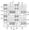
図3は、本実施形態の画素の概略構成の一例を示す平面図である。なお、図3では、2×2の4画素分の構成について示している。本実施形態の固体撮像装置が有する画素は4画素に限定されないということは言うまでもない。
As described above, in this embodiment, at time t3 to t4, at least a part of the electric charge overflowing from the photodiode PD is caused to flow into the floating diffusion region FD via the
FIG. 3 is a plan view illustrating an example of a schematic configuration of the pixel of the present embodiment. Note that FIG. 3 shows a configuration for 2 × 2 pixels. It goes without saying that the pixels of the solid-state imaging device of the present embodiment are not limited to four pixels.
図3において、21a〜21dは、フォトダイオードであり、図1のフォトダイオードFDに対応するものである。22a〜22dは、第1の転送MOSトランジスタであり、図1の第1の転送MOSトランジスタM1に対応するものである。23a〜23dは、フローティングディフュージョン領域であり、図1のフローティングディフュージョン領域FDに対応するものである。
In FIG. 3,
24は、ポテンシャル障壁形成用P型層である。25a〜25dは、フォトダイオード21a〜21d及び第1の転送MOSトランジスタ22a〜22d以外の素子群である。具体的に素子群25a〜25dとしては、図1に示したリセットMOSトランジスタM2、第2の転送MOSトランジスタM3、ソースフォロアMOSトランジスタM4、選択MOSトランジスタM5、及び付加容量CS等がある。また、図3の太線で示す領域は、各素子における拡散層(N+層)を示している。
本実施形態では、フォトダイオード21a〜21d、第1の転送MOSトランジスタ22a〜22d、及び素子群25a〜25dが、P型のウェル(Pウェル)上に形成されている。
In the present embodiment, the
ポテンシャル障壁形成用P型層24は、Pウェルよりも高濃度のP型不純物が含まれている層である。このような高濃度のP型領域であるポテンシャル障壁形成用P型層24は、第1の転送MOSトランジスタ22a〜22dのゲートの下方を除くPウェル内の領域に形成されている。ただし、Pウェルの深さ方向の全体に亘ってポテンシャル障壁形成用P型層24が形成されている必要はなく、経路31を形成するのに必要な領域よりも深い領域には、ポテンシャル障壁形成用P型層24を形成しないようにしてもよい。
The potential barrier forming P-
図4は、図3のA−B方向から見た画素を簡略化して示した図である。図4(a)は、図3のA−B方向から見た画素の様子と、その画素の深さ方向におけるポテンシャルの分布とを簡略化して示した図である。図4(b)は、経路31内の所定の位置における電荷蓄積時のポテンシャルを示した図である。図4(c)は、経路31内の所定の位置における電荷転送時のポテンシャルを示した図である。
FIG. 4 is a diagram showing the pixels viewed from the direction AB in FIG. 3 in a simplified manner. FIG. 4A is a diagram schematically illustrating the state of the pixel viewed from the AB direction in FIG. 3 and the potential distribution in the depth direction of the pixel. FIG. 4B is a diagram showing the potential at the time of charge accumulation at a predetermined position in the
図4(a)において、本実施形態では、ポテンシャル障壁形成用P型層24として、第1の濃度を有するチャネルストップ領域(またこのチャネルストップ領域もポテンシャル障壁形成用P型層として用いても良い。)24aと、第2の濃度を有する第2のポテンシャル障壁形成用P型層24bと、第3の濃度を有する第3のポテンシャル障壁形成用P型層24cとが積層された構造を有している。
4A, in this embodiment, as the potential barrier forming P-
また、本実施形態では、第2のポテンシャル障壁形成用P型層24bにおけるP型不純物濃度を、その第2のポテンシャル障壁形成用P型層24bの上下に形成された第1のポテンシャル障壁形成用P型層24a及び第3のポテンシャル障壁形成用P型層24cよりも低くしている。このようにすると、図4(a)に示すように、第1の転送MOSトランジスタ22a〜22dのゲートの下方の領域のうち、第2のポテンシャル障壁形成用P型層24bが形成されている領域と同じ位の深さにある領域のポテンシャルを最も低くすることができる。このように、本実施形態では、第2のポテンシャル障壁形成用P型層24bにおける深さ方向の濃度を変えることにより、経路31におけるポテンシャルを調節できるようにしている。
In the present embodiment, the P-type impurity concentration in the second potential barrier forming P-
具体的に、経路31は、第1の転送MOSトランジスタ22a〜22dのソース及びドレイン間に形成されるチャネルよりも深い位置(すなわち、チャネルの下方)に形成されるようにする。この場合、第1の転送MOSトランジスタ22a〜22dのゲート電位の影響を受けないように、なるべく深い位置に経路31が形成されるようにするのが好ましい。ただし、前述したように経路31は、フォトダイオード21から溢れた電荷を流入するものである。このため、経路31は、フォトダイオード21の下端よりも浅い位置に形成されるようにする必要がある。
Specifically, the
フォトダイオード21や、フローティングディフュージョン領域23に電荷を蓄積する場合には、第1の転送MOSトランジスタ22のゲートにおけるポテンシャル(ゲート電位)Vg、経路31におけるポテンシャルOFD、フォトダイオード21のポテンシャルPD、フローティングディフュージョン領域23におけるポテンシャルFD、及び経路31の横方向(図3のA−B方向)の領域(ポテンシャル障壁形成用P型層24)におけるポテンシャルAPは、図4(b)に示すようにして与えられる。
When charges are accumulated in the photodiode 21 or the floating diffusion region 23, the potential (gate potential) Vg at the gate of the first
図4に示すようにして、ポテンシャル障壁形成用P型層24を形成することにより、第1の転送MOSトランジスタ22のゲートの下方にある経路31のポテンシャルOFDを低くすることができる。これにより、フォトダイオード21への電荷の蓄積動作時にフォトダイオード21から溢れた電荷を経路31に流入させることができる。
As shown in FIG. 4, by forming the potential barrier forming P-
以上のように本実施形態では、第1のMOSトランジスタ22のゲートの下方の領域を除くPウェル内の領域にポテンシャル障壁形成用P型層24を形成するようにした。これにより、電荷を蓄積する際に、第1の転送MOSトランジスタ22のゲート電位Vgを−1[V]にして、第1の転送MOSトランジスタ22のゲートの直下の領域におけるポテンシャルを上げても(第1の転送MOSトランジスタ22を可及的に確実にオフしても)、フォトダイオード21から溢れた電荷を経路31に流入させることができる。これにより、第1の転送MOSトランジスタ22のゲートの直下の領域が空乏領域になるのを防止して、第1の転送MOSトランジスタ22のゲート酸化膜41の界面から暗電流が発生するのを可及的に防止することと、経路31を介してフローティングディフュージョン領域FDに蓄積された電荷を用いて、固体撮像装置のダイナミックレンジを拡大することとを同時に実現できる。
As described above, in the present embodiment, the potential barrier forming P-
一方、フォトダイオード21から電荷を転送する場合には、第1の転送MOSトランジスタ22のゲート電位Vg、経路31におけるポテンシャルOFD、フォトダイオード21のポテンシャルPD、フローティングディフュージョン領域23におけるポテンシャルFD、及び経路31の横方向の領域(ポテンシャル障壁形成用P型層24)におけるポテンシャルAPは、図4(c)に示すようにして与えられる。
On the other hand, when transferring charges from the photodiode 21, the gate potential Vg of the first
このように、電荷を転送する場合には、第1の転送MOSトランジスタ22のゲート電位Vgを5[V]にして、第1の転送MOSトランジスタ22のゲートの直下の領域(チャネル領域)におけるポテンシャルを下げるようにしている。これにより、フォトダイオード21に蓄積された電荷がフローティングディフュージョン領域23に確実に転送させることができる。
As described above, when transferring charges, the gate potential Vg of the first
なお、本実施形態では、電荷蓄積時における第1の転送MOSトランジスタ22のゲート電位Vgを−1[V]にし、電荷転送時における第1の転送MOSトランジスタ22のゲート電位Vgを−1[V]にしたが、第1の転送MOSトランジスタ22のゲート電位Vgは、これらに限定されないということは言うまでもない。
また、本実施形態のように、第2の転送MOSトランジスタM3と、付加容量CSとを用いれば、固体撮像装置のダイナミックレンジをより拡大させることができ好ましいが、必ずしも第2の転送MOSトランジスタM3と、付加容量CSとを用いる必要はない。
In the present embodiment, the gate potential Vg of the first
In addition, if the second transfer MOS transistor M3 and the additional capacitor CS are used as in the present embodiment, the dynamic range of the solid-state imaging device can be further expanded. However, the second transfer MOS transistor M3 is not necessarily used. It is not necessary to use the additional capacitor CS.
さらに、本実施形態では、ポテンシャル障壁形成用P型層24を設けるようにしたが、経路31におけるP型不純物濃度が、経路31の横方向(図3のA−B方向)の領域よりも相対的に低くなるようにすれば(経路31におけるポテンシャルを、経路31の側方向(図3のA−B方向)の領域よりも低くするようにすれば)、必ずしもポテンシャル障壁形成用P型層24を設ける必要はない。例えば、図4(a)における経路31が形成されている位置にn型不純物を添加するようにしてもよい。
また、ポテンシャル障壁形成用P型層24の形成領域はトランジスタの下部領域も含めて形成しても良いし、図5に示すようにフォトダイオードPDが形成されている領域を少なくとも覆うように形成しても良い。
Furthermore, in the present embodiment, the P-
Further, the formation region of the P-
(他の実施形態)
図6に基づいて、前述した実施形態の固体撮像装置をスチルカメラに適用した場合の一実施形態について詳述する。
図6は、前述した実施形態の固体撮像装置を「スチルビデオカメラ」に適用した場合を示すブロック図である。
図6において、1301は、レンズのプロテクトとメインスイッチを兼ねるバリアであり、1302は、被写体の光学像を固体撮像素子1304に結像させるレンズであり、1303は、レンズ1302を通った光量を可変するための絞りであり、1304は、レンズ1302で結像された被写体を画像信号として取り込むための固体撮像素子であり、1306は、固体撮像素子1304より出力される画像信号のアナログーディジタル変換を行うA/D変換器である。
(Other embodiments)
Based on FIG. 6, one embodiment when the solid-state imaging device of the above-described embodiment is applied to a still camera will be described in detail.
FIG. 6 is a block diagram showing a case where the solid-state imaging device of the above-described embodiment is applied to a “still video camera”.
In FIG. 6,
1307は、A/D変換器1306より出力された画像データに各種の補正を行ったりデータを圧縮したりする信号処理部であり、1308は、固体撮像素子1304、撮像信号処理回路1305、A/D変換器1306、及び信号処理部1307に、各種タイミング信号を出力するタイミング発生部であり、1309は、各種演算とスチルビデオカメラ全体を制御する全体制御・演算部であり、1310は、画像データを一時的に記憶する為のメモリ部であり、1311は、記録媒体に記録または読み出しを行うためのインターフェース部であり、1312は、画像データの記録または読み出しを行う為の半導体メモリ等の着脱可能な記録媒体であり、1313は、外部コンピュータ等と通信する為のインターフェース部である。
A
次に、前述の構成における撮影時のスチルビデオカメラの動作について説明する。
バリア1301がオープンされるとメイン電源がオンされ、次にコントロール系の電源がオンし、更にA/D変換器1306などの撮像系回路の電源がオンされる。
それから、露光量を制御する為に、全体制御・演算部1309は絞り1303を開放にし、固体撮像素子1304から出力された信号はA/D変換器1306で変換された後、信号処理部1307に入力される。
そのデータを基に露出の演算を全体制御・演算部1309で行う。
この測光を行った結果により明るさを判断し、その結果に応じて全体制御・演算部1309は絞りを制御する。
Next, the operation of the still video camera at the time of shooting in the above configuration will be described.
When the
Then, in order to control the exposure amount, the overall control /
Based on the data, the exposure control is performed by the overall control /
The brightness is determined based on the result of the photometry, and the overall control /
固体撮像素子1304から出力された信号をもとに、高周波成分を取り出し被写体までの距離の演算を全体制御・演算部1309で行う。その後、レンズを駆動して合焦か否かを判断し、合焦していないと判断した時は、再びレンズを駆動し測距を行う。
そして、合焦が確認された後に本露光が始まる。
露光が終了すると、固体撮像素子1304から出力された画像信号はA/D変換器1306でA/D変換され、信号処理部1307を通り全体制御・演算部1309によりメモリ部に書き込まれる。
Based on the signal output from the solid-
Then, after the in-focus state is confirmed, the main exposure starts.
When the exposure is completed, the image signal output from the solid-
その後、メモリ部1310に蓄積されたデータは、全体制御・演算部1309の制御により記録媒体制御I/F部を通り半導体メモリ等の着脱可能な記録媒体1312に記録される。また、外部I/F部1313を通り直接コンピュータ等に入力して画像の加工を行ってもよい。
Thereafter, the data stored in the
次に、図7に基づいて、前述した実施形態の固体撮像装置をビデオカメラに適用した場合の一実施例について詳述する。
図7は、前述した実施形態の固体撮像装置を「ビデオカメラ」に適用した場合を示すブロック図である。図7において、1401は撮影レンズであり、焦点調節を行うためのフォーカスレンズ1401A、ズーム動作を行うズームレンズ1401B、及び結像用のレンズ1401Cを備えている。
1402は絞りであり、1403は、撮像面に結像された被写体像を光電変換して電気的な撮像信号に変換する固体撮像素子であり、1404は、固体撮像素子3より出力された撮像信号をサンプルホールドし、さらに、レベルをアンプするサンプルホールド回路(S/H回路)であり、映像信号を出力する。
Next, an example when the solid-state imaging device of the above-described embodiment is applied to a video camera will be described in detail with reference to FIG.
FIG. 7 is a block diagram showing a case where the solid-state imaging device of the above-described embodiment is applied to a “video camera”. In FIG. 7,
1402 is a stop, 1403 is a solid-state image sensor that photoelectrically converts an object image formed on the imaging surface into an electrical image signal, and 1404 is an image signal output from the solid-
1405は、サンプルホールド回路1404から出力された映像信号にガンマ補正、色分離、ブランキング処理等の所定の処理を施すプロセス回路であり、輝度信号Yおよびクロマ信号Cを出力する。プロセス回路1405から出力されたクロマ信号Cは、色信号補正回路1421で、ホワイトバランス及び色バランスの補正がなされ、色差信号R−Y,B−Yとして出力される。
また、プロセス回路1405から出力された輝度信号Yと、色信号補正回路1421から出力された色差信号R−Y,B−Yとは、エンコーダ回路(ENC回路)1424で変調され、標準テレビジョン信号として出力される。そして、図示しないビデオレコーダ、あるいはモニタEVF(Electric View Finder)等の電子ビューファインダへと供給される。
1406はアイリス制御回路であり、サンプルホールド回路1404から供給される映像信号に基づいてアイリス駆動回路1407を制御し、映像信号のレベルが所定レベルの一定値となるように、絞り1402の開口量を制御すべくigメータを自動制御するものである。
In addition, the luminance signal Y output from the
1413、1414は、サンプルホールド回路1404から出力された映像信号中より合焦検出を行うために必要な高周波成分を抽出する異なった帯域制限のバンドパスフィルタ(BPF)である。第一のバンドパスフィルタ1413(BPF1)、及び第2のバンドパスフィルタ1414(BPF2)から出力された信号は、ゲート回路1415及びフォーカスゲート枠信号で各々ゲートされ、ピーク検出回路1416でピーク値が検出されてホールドされると共に、論理制御回路1417に入力される。
この信号を焦点電圧と呼び、この焦点電圧によってフォーカスを合わせている。
This signal is called a focus voltage, and the focus is adjusted by this focus voltage.
また、1418はフォーカスレンズ1401Aの移動位置を検出するフォーカスエンコーダであり、1419はズームレンズ1401Bの焦点距離を検出するズームエンコーダであり、1420は絞り1402の開口量を検出するアイリスエンコーダである。これらのエンコーダの検出値は、システムコントロールを行う論理制御回路1417へと供給される。
論理制御回路1417は、設定された合焦検出領域内に相当する映像信号に基づいて、被写体に対する合焦検出を行い、焦点調節を行う。即ち、各々のバンドパスフィルタ1413、1414より供給された高周波成分のピーク値情報を取り込み、高周波成分のピーク値が最大となる位置へとフォーカスレンズ1401Aを駆動すべくフォーカス駆動回路1409にフォーカスモータ1410の回転方向、回転速度、回転/停止等の制御信号を供給し、これを制御する。
The
なお、前述した各実施形態は、何れも本発明を実現するにあがっての具体化のほんの一例を示したものに過ぎず、これらによって本発明の技術的範囲が限定的に解釈されていはならない。 It should be noted that each of the above-described embodiments is merely an example of realization of the present invention, and the technical scope of the present invention should not be construed in a limited manner. .
CS 付加容量
M2 リセットMOSトランジスタ
M3 第2の転送MOSトランジスタ
M4 ソースフォロアMOSトランジスタ
M5 選択MOSトランジスタ
21、PD フォトダイオード
22、M1 第1の転送MOSトランジスタ
23、FD フローティングディフュージョン領域
24 ポテンシャル障壁形成用P型層
31 経路
CS additional capacitor M2 reset MOS transistor M3 second transfer MOS transistor M4 source follower MOS transistor M5 selection MOS transistor 21,
Claims (6)
入射した光によって電荷を生成する光電変換部と、
前記光電変換部で生成した電荷を電荷蓄積領域へ転送するための転送MOSトランジスタと、
前記光電変換部から溢れた電荷の少なくとも一部が前記電荷蓄積領域に移動する際の経路と、
前記電荷に対するポテンシャル障壁層と、を有する画素を複数含み、
前記経路は、前記半導体基板内の第1の導電型のウエル内であって、前記転送MOSトランジスタのチャネル領域よりも前記半導体基板の深部に形成されており、
前記ポテンシャル障壁層は、前記転送MOSトランジスタのゲート電極の下方を除く前記第1の導電型のウエル内の領域に設けられた、前記第1の導電型のウエルよりも前記第1の導電型の不純物濃度が高い第1の導電型の領域であり、
前記経路における第1の導電型の不純物濃度は、前記ポテンシャル障壁層の前記第1の導電型の不純物濃度よりも低く、
前記転送MOSトランジスタの前記ゲート電極の幅方向の断面において、前記経路は、前記幅方向で前記ポテンシャル障壁層に挟まれるように、前記ポテンシャル障壁層の間に配置されていることを特徴とする固体撮像装置。 A semiconductor substrate;
A photoelectric conversion unit that generates charges by incident light; and
A transfer MOS transistor for transferring the charge generated by the photoelectric conversion unit to the charge storage region;
A path when at least a part of the charge overflowing from the photoelectric conversion unit moves to the charge accumulation region;
A plurality of pixels having a potential barrier layer for the charge,
The path is formed in a well of the first conductivity type in the semiconductor substrate, and is formed deeper in the semiconductor substrate than the channel region of the transfer MOS transistor.
The potential barrier layer is provided in a region within the well of the first conductivity type except under the gate electrode of the transfer MOS transistor, and has the first conductivity type rather than the well of the first conductivity type. A first conductivity type region having a high impurity concentration;
The impurity concentration of the first conductivity type in the path is lower than the impurity concentration of the first conductivity type of the potential barrier layer,
In the width direction of the cross section of the gate electrode of the transfer MOS transistor, the path, so as to be sandwiched between the potential barrier layer in the width direction, characterized in that it is placed between the potential barrier layer Solid-state imaging device.
前記経路は、前記第2の導電型の半導体領域の下端よりも浅い位置に形成されていることを特徴とする請求項2に記載の固体撮像装置。 The photoelectric conversion unit is formed of a second conductivity type semiconductor region for accumulating the charge, and the first conductivity type well .
The solid-state imaging device according to claim 2 , wherein the path is formed at a position shallower than a lower end of the second conductive type semiconductor region.
前記固体撮像装置に光学像を結像させるためのレンズと、
前記レンズを通る光量を可変するための絞りとを有することを特徴とするカメラ。 A solid-state imaging device according to any one of claims 1 to 5 ,
A lens for forming an optical image on the solid-state imaging device;
And a diaphragm for varying the amount of light passing through the lens.
Priority Applications (2)
| Application Number | Priority Date | Filing Date | Title |
|---|---|---|---|
| JP2005080343A JP4794877B2 (en) | 2005-03-18 | 2005-03-18 | Solid-state imaging device and camera |
| US11/376,213 US7550793B2 (en) | 2005-03-18 | 2006-03-16 | Image pickup device and camera with expanded dynamic range |
Applications Claiming Priority (1)
| Application Number | Priority Date | Filing Date | Title |
|---|---|---|---|
| JP2005080343A JP4794877B2 (en) | 2005-03-18 | 2005-03-18 | Solid-state imaging device and camera |
Related Child Applications (1)
| Application Number | Title | Priority Date | Filing Date |
|---|---|---|---|
| JP2011103093A Division JP5361938B2 (en) | 2011-05-02 | 2011-05-02 | Solid-state imaging device and camera |
Publications (3)
| Publication Number | Publication Date |
|---|---|
| JP2006261595A JP2006261595A (en) | 2006-09-28 |
| JP2006261595A5 JP2006261595A5 (en) | 2008-05-01 |
| JP4794877B2 true JP4794877B2 (en) | 2011-10-19 |
Family
ID=37009405
Family Applications (1)
| Application Number | Title | Priority Date | Filing Date |
|---|---|---|---|
| JP2005080343A Expired - Fee Related JP4794877B2 (en) | 2005-03-18 | 2005-03-18 | Solid-state imaging device and camera |
Country Status (2)
| Country | Link |
|---|---|
| US (1) | US7550793B2 (en) |
| JP (1) | JP4794877B2 (en) |
Families Citing this family (95)
| Publication number | Priority date | Publication date | Assignee | Title |
|---|---|---|---|---|
| US7294818B2 (en) * | 2004-08-24 | 2007-11-13 | Canon Kabushiki Kaisha | Solid state image pickup device and image pickup system comprising it |
| JP4756839B2 (en) * | 2004-09-01 | 2011-08-24 | キヤノン株式会社 | Solid-state imaging device and camera |
| JP4916101B2 (en) * | 2004-09-01 | 2012-04-11 | キヤノン株式会社 | Photoelectric conversion device, solid-state imaging device, and solid-state imaging system |
| JP5089017B2 (en) * | 2004-09-01 | 2012-12-05 | キヤノン株式会社 | Solid-state imaging device and solid-state imaging system |
| JP4971586B2 (en) | 2004-09-01 | 2012-07-11 | キヤノン株式会社 | Solid-state imaging device |
| JP4416668B2 (en) * | 2005-01-14 | 2010-02-17 | キヤノン株式会社 | Solid-state imaging device, control method thereof, and camera |
| JP2006197392A (en) * | 2005-01-14 | 2006-07-27 | Canon Inc | Solid-state imaging device, camera, and method of driving solid-state imaging device |
| JP4459064B2 (en) * | 2005-01-14 | 2010-04-28 | キヤノン株式会社 | Solid-state imaging device, control method thereof, and camera |
| JP4677258B2 (en) | 2005-03-18 | 2011-04-27 | キヤノン株式会社 | Solid-state imaging device and camera |
| JP4459098B2 (en) | 2005-03-18 | 2010-04-28 | キヤノン株式会社 | Solid-state imaging device and camera |
| JP4459099B2 (en) * | 2005-03-18 | 2010-04-28 | キヤノン株式会社 | Solid-state imaging device and camera |
| JP4827508B2 (en) | 2005-12-02 | 2011-11-30 | キヤノン株式会社 | Imaging system |
| US7700471B2 (en) * | 2005-12-13 | 2010-04-20 | Versatilis | Methods of making semiconductor-based electronic devices on a wire and articles that can be made thereby |
| JP2007242697A (en) * | 2006-03-06 | 2007-09-20 | Canon Inc | Image pickup device and image pickup system |
| KR101255334B1 (en) * | 2006-05-08 | 2013-04-16 | 페어차일드코리아반도체 주식회사 | Power module for low thermal resistance and method of fabricating of the same power module |
| JP4804254B2 (en) * | 2006-07-26 | 2011-11-02 | キヤノン株式会社 | Photoelectric conversion device and imaging device |
| JP4818018B2 (en) * | 2006-08-01 | 2011-11-16 | キヤノン株式会社 | Photoelectric conversion device and imaging system using the same |
| JP4956084B2 (en) * | 2006-08-01 | 2012-06-20 | キヤノン株式会社 | Photoelectric conversion device and imaging system using the same |
| JP5110820B2 (en) * | 2006-08-02 | 2012-12-26 | キヤノン株式会社 | Photoelectric conversion device, photoelectric conversion device manufacturing method, and imaging system |
| JP4185949B2 (en) * | 2006-08-08 | 2008-11-26 | キヤノン株式会社 | Photoelectric conversion device and imaging device |
| JP4928199B2 (en) * | 2006-09-07 | 2012-05-09 | キヤノン株式会社 | Signal detection device, signal readout method of signal detection device, and imaging system using signal detection device |
| JP5173171B2 (en) * | 2006-09-07 | 2013-03-27 | キヤノン株式会社 | PHOTOELECTRIC CONVERSION DEVICE, IMAGING DEVICE, AND SIGNAL READING METHOD |
| JP5043388B2 (en) * | 2006-09-07 | 2012-10-10 | キヤノン株式会社 | Solid-state imaging device and imaging system |
| JP5584982B2 (en) | 2009-02-09 | 2014-09-10 | ソニー株式会社 | Solid-state imaging device and camera system |
| JP2008205638A (en) * | 2007-02-16 | 2008-09-04 | Texas Instr Japan Ltd | Solid-state imaging device and its operation method |
| JP2008205639A (en) * | 2007-02-16 | 2008-09-04 | Texas Instr Japan Ltd | Solid-state imaging device and its operation method |
| JP4054839B1 (en) | 2007-03-02 | 2008-03-05 | キヤノン株式会社 | Photoelectric conversion device and imaging system using the same |
| JP4931233B2 (en) * | 2007-07-04 | 2012-05-16 | キヤノン株式会社 | Imaging apparatus and processing method thereof |
| JP4931232B2 (en) * | 2007-07-04 | 2012-05-16 | キヤノン株式会社 | Imaging apparatus and processing method thereof |
| JP2009021809A (en) * | 2007-07-11 | 2009-01-29 | Canon Inc | Driving method of imaging device, imaging device, and imaging system |
| JP4991436B2 (en) * | 2007-08-02 | 2012-08-01 | キヤノン株式会社 | Imaging apparatus and imaging system |
| EP2037667B1 (en) * | 2007-09-14 | 2017-08-23 | Canon Kabushiki Kaisha | Image sensing apparatus and imaging system |
| JP4548519B2 (en) * | 2007-10-16 | 2010-09-22 | セイコーエプソン株式会社 | Light source device |
| JP2009141631A (en) * | 2007-12-05 | 2009-06-25 | Canon Inc | Photoelectric conversion device and image pickup device |
| JP5366396B2 (en) * | 2007-12-28 | 2013-12-11 | キヤノン株式会社 | Photoelectric conversion device manufacturing method, semiconductor device manufacturing method, photoelectric conversion device, and imaging system |
| JP4685120B2 (en) | 2008-02-13 | 2011-05-18 | キヤノン株式会社 | Photoelectric conversion device and imaging system |
| JP5371463B2 (en) | 2008-02-28 | 2013-12-18 | キヤノン株式会社 | IMAGING DEVICE, IMAGING SYSTEM, AND IMAGING DEVICE CONTROL METHOD |
| JP5268389B2 (en) | 2008-02-28 | 2013-08-21 | キヤノン株式会社 | Solid-state imaging device, driving method thereof, and imaging system |
| JP5156434B2 (en) * | 2008-02-29 | 2013-03-06 | キヤノン株式会社 | Imaging apparatus and imaging system |
| JP5328207B2 (en) * | 2008-04-01 | 2013-10-30 | キヤノン株式会社 | Solid-state imaging device |
| JP5102115B2 (en) * | 2008-06-05 | 2012-12-19 | キヤノン株式会社 | Imaging apparatus and imaging system |
| JP5279352B2 (en) | 2008-06-06 | 2013-09-04 | キヤノン株式会社 | Solid-state imaging device |
| JP5161676B2 (en) * | 2008-07-07 | 2013-03-13 | キヤノン株式会社 | Imaging apparatus and imaging system |
| JP5089514B2 (en) * | 2008-07-11 | 2012-12-05 | キヤノン株式会社 | Imaging apparatus and imaging system |
| US8913166B2 (en) * | 2009-01-21 | 2014-12-16 | Canon Kabushiki Kaisha | Solid-state imaging apparatus |
| JP5478905B2 (en) * | 2009-01-30 | 2014-04-23 | キヤノン株式会社 | Solid-state imaging device |
| JP5257134B2 (en) * | 2009-02-25 | 2013-08-07 | コニカミノルタビジネステクノロジーズ株式会社 | Solid-state imaging device and imaging apparatus including the same |
| JP5235814B2 (en) * | 2009-08-04 | 2013-07-10 | キヤノン株式会社 | Solid-state imaging device |
| JP5679653B2 (en) * | 2009-12-09 | 2015-03-04 | キヤノン株式会社 | Photoelectric conversion device and imaging system using the same |
| JP5780711B2 (en) | 2010-04-06 | 2015-09-16 | キヤノン株式会社 | Solid-state imaging device |
| JP5645513B2 (en) | 2010-07-07 | 2014-12-24 | キヤノン株式会社 | Solid-state imaging device and imaging system |
| JP5697371B2 (en) | 2010-07-07 | 2015-04-08 | キヤノン株式会社 | Solid-state imaging device and imaging system |
| JP5885401B2 (en) | 2010-07-07 | 2016-03-15 | キヤノン株式会社 | Solid-state imaging device and imaging system |
| JP5656484B2 (en) | 2010-07-07 | 2015-01-21 | キヤノン株式会社 | Solid-state imaging device and imaging system |
| JP5643555B2 (en) | 2010-07-07 | 2014-12-17 | キヤノン株式会社 | Solid-state imaging device and imaging system |
| JP5751766B2 (en) | 2010-07-07 | 2015-07-22 | キヤノン株式会社 | Solid-state imaging device and imaging system |
| JP5762199B2 (en) | 2011-07-28 | 2015-08-12 | キヤノン株式会社 | Solid-state imaging device |
| JP5858695B2 (en) | 2011-09-08 | 2016-02-10 | キヤノン株式会社 | Solid-state imaging device and driving method of solid-state imaging device |
| JP5864990B2 (en) | 2011-10-03 | 2016-02-17 | キヤノン株式会社 | Solid-state imaging device and camera |
| JP5901212B2 (en) | 2011-10-07 | 2016-04-06 | キヤノン株式会社 | Photoelectric conversion system |
| JP5484422B2 (en) | 2011-10-07 | 2014-05-07 | キヤノン株式会社 | Solid-state imaging device |
| JP5930651B2 (en) | 2011-10-07 | 2016-06-08 | キヤノン株式会社 | Solid-state imaging device |
| JP5967912B2 (en) | 2011-12-02 | 2016-08-10 | キヤノン株式会社 | Solid-state imaging device |
| JP5967915B2 (en) | 2011-12-09 | 2016-08-10 | キヤノン株式会社 | Driving method of solid-state imaging device |
| JP5967944B2 (en) | 2012-01-18 | 2016-08-10 | キヤノン株式会社 | Solid-state imaging device and camera |
| JP6023437B2 (en) | 2012-02-29 | 2016-11-09 | キヤノン株式会社 | Solid-state imaging device and camera |
| JP5956840B2 (en) | 2012-06-20 | 2016-07-27 | キヤノン株式会社 | Solid-state imaging device and camera |
| JP2014112760A (en) * | 2012-12-05 | 2014-06-19 | Sony Corp | Solid-state image pickup device and electronic apparatus |
| JP6108884B2 (en) | 2013-03-08 | 2017-04-05 | キヤノン株式会社 | Photoelectric conversion device and imaging system |
| JP2014175553A (en) | 2013-03-11 | 2014-09-22 | Canon Inc | Solid-state imaging device and camera |
| JP6174901B2 (en) | 2013-05-10 | 2017-08-02 | キヤノン株式会社 | Solid-state imaging device and camera |
| JP5886806B2 (en) | 2013-09-17 | 2016-03-16 | キヤノン株式会社 | Solid-state imaging device |
| JP6245997B2 (en) | 2014-01-16 | 2017-12-13 | キヤノン株式会社 | Solid-state imaging device and imaging system |
| JP6057931B2 (en) | 2014-02-10 | 2017-01-11 | キヤノン株式会社 | Photoelectric conversion device and imaging system using the same |
| JP6541347B2 (en) | 2014-03-27 | 2019-07-10 | キヤノン株式会社 | Solid-state imaging device and imaging system |
| JP6548391B2 (en) | 2014-03-31 | 2019-07-24 | キヤノン株式会社 | Photoelectric conversion device and imaging system |
| JP6385192B2 (en) | 2014-08-14 | 2018-09-05 | キヤノン株式会社 | Imaging apparatus, imaging system, and driving method of imaging system |
| JP6109125B2 (en) | 2014-08-20 | 2017-04-05 | キヤノン株式会社 | Semiconductor device, solid-state imaging device, and imaging system |
| JP2016111425A (en) | 2014-12-03 | 2016-06-20 | ルネサスエレクトロニクス株式会社 | Imaging apparatus |
| US9900539B2 (en) | 2015-09-10 | 2018-02-20 | Canon Kabushiki Kaisha | Solid-state image pickup element, and image pickup system |
| JP6732468B2 (en) | 2016-02-16 | 2020-07-29 | キヤノン株式会社 | Photoelectric conversion device and driving method thereof |
| JP6738200B2 (en) | 2016-05-26 | 2020-08-12 | キヤノン株式会社 | Imaging device |
| US10319765B2 (en) | 2016-07-01 | 2019-06-11 | Canon Kabushiki Kaisha | Imaging device having an effective pixel region, an optical black region and a dummy region each with pixels including a photoelectric converter |
| JP6740067B2 (en) | 2016-09-16 | 2020-08-12 | キヤノン株式会社 | Solid-state imaging device and driving method thereof |
| JP6436953B2 (en) | 2016-09-30 | 2018-12-12 | キヤノン株式会社 | Solid-state imaging device, driving method thereof, and imaging system |
| JP6750876B2 (en) | 2016-10-07 | 2020-09-02 | キヤノン株式会社 | Solid-state imaging device and driving method thereof |
| JP6552478B2 (en) | 2016-12-28 | 2019-07-31 | キヤノン株式会社 | Solid-state imaging device |
| US10652531B2 (en) | 2017-01-25 | 2020-05-12 | Canon Kabushiki Kaisha | Solid-state imaging device, imaging system, and movable object |
| JP2019087939A (en) | 2017-11-09 | 2019-06-06 | キヤノン株式会社 | Photoelectric conversion device, electronic equipment, conveyance apparatus and drive method of photoelectric conversion device |
| JP6704893B2 (en) | 2017-11-30 | 2020-06-03 | キヤノン株式会社 | Solid-state imaging device, imaging system, and method for driving solid-state imaging device |
| JP7214454B2 (en) | 2018-12-06 | 2023-01-30 | キヤノン株式会社 | Photoelectric conversion element and imaging device |
| JP7336206B2 (en) | 2019-02-27 | 2023-08-31 | キヤノン株式会社 | Method for manufacturing photoelectric conversion device |
| JP7374639B2 (en) | 2019-07-19 | 2023-11-07 | キヤノン株式会社 | Photoelectric conversion device and imaging system |
| JP7303682B2 (en) | 2019-07-19 | 2023-07-05 | キヤノン株式会社 | Photoelectric conversion device and imaging system |
| JP2021136634A (en) | 2020-02-28 | 2021-09-13 | キヤノン株式会社 | Imaging device and imaging system |
Family Cites Families (42)
| Publication number | Priority date | Publication date | Assignee | Title |
|---|---|---|---|---|
| US5245203A (en) * | 1988-06-06 | 1993-09-14 | Canon Kabushiki Kaisha | Photoelectric converter with plural regions |
| US5352920A (en) * | 1988-06-06 | 1994-10-04 | Canon Kabushiki Kaisha | Photoelectric converter with light shielding sections |
| US5261013A (en) * | 1989-02-21 | 1993-11-09 | Canon Kabushiki Kaisha | Photoelectric converter and image reading apparatus mounting the same |
| GB2262658B (en) * | 1989-02-21 | 1993-09-29 | Canon Kk | Photoelectric converter |
| JP3067435B2 (en) * | 1992-12-24 | 2000-07-17 | キヤノン株式会社 | Image reading photoelectric conversion device and image processing apparatus having the device |
| JPH08186241A (en) * | 1995-01-06 | 1996-07-16 | Canon Inc | Image pick-up element, and solid image pickup device |
| TW421962B (en) * | 1997-09-29 | 2001-02-11 | Canon Kk | Image sensing device using mos type image sensing elements |
| JPH11261046A (en) * | 1998-03-12 | 1999-09-24 | Canon Inc | Solid-state image pickup device |
| JPH11274454A (en) * | 1998-03-19 | 1999-10-08 | Canon Inc | Solid image pick-up device and its forming method |
| JP3403061B2 (en) * | 1998-03-31 | 2003-05-06 | 株式会社東芝 | Solid-state imaging device |
| JP3571909B2 (en) * | 1998-03-19 | 2004-09-29 | キヤノン株式会社 | Solid-state imaging device and method of manufacturing the same |
| JP3308904B2 (en) * | 1998-06-24 | 2002-07-29 | キヤノン株式会社 | Solid-state imaging device |
| US6307195B1 (en) * | 1999-10-26 | 2001-10-23 | Eastman Kodak Company | Variable collection of blooming charge to extend dynamic range |
| JP3467013B2 (en) * | 1999-12-06 | 2003-11-17 | キヤノン株式会社 | Solid-state imaging device |
| JP3724374B2 (en) * | 2001-01-15 | 2005-12-07 | ソニー株式会社 | Solid-state imaging device and driving method thereof |
| US20030076431A1 (en) * | 2001-10-24 | 2003-04-24 | Krymski Alexander I. | Image sensor with pixels having multiple capacitive storage elements |
| EP1341377B1 (en) * | 2002-02-27 | 2018-04-11 | Canon Kabushiki Kaisha | Signal processing device for image pickup apparatus |
| JP3728260B2 (en) * | 2002-02-27 | 2005-12-21 | キヤノン株式会社 | Photoelectric conversion device and imaging device |
| JP3840203B2 (en) * | 2002-06-27 | 2006-11-01 | キヤノン株式会社 | Solid-state imaging device and camera system using the solid-state imaging device |
| JP4208559B2 (en) * | 2002-12-03 | 2009-01-14 | キヤノン株式会社 | Photoelectric conversion device |
| JP3840214B2 (en) * | 2003-01-06 | 2006-11-01 | キヤノン株式会社 | Photoelectric conversion device, method for manufacturing photoelectric conversion device, and camera using the same |
| JP4484449B2 (en) * | 2003-05-08 | 2010-06-16 | 富士フイルム株式会社 | Solid-state imaging device |
| JP4155568B2 (en) * | 2003-08-07 | 2008-09-24 | キヤノン株式会社 | Solid-state imaging device and camera |
| JP4514188B2 (en) * | 2003-11-10 | 2010-07-28 | キヤノン株式会社 | Photoelectric conversion device and imaging device |
| JP4508619B2 (en) * | 2003-12-03 | 2010-07-21 | キヤノン株式会社 | Method for manufacturing solid-state imaging device |
| JP3793202B2 (en) * | 2004-02-02 | 2006-07-05 | キヤノン株式会社 | Solid-state imaging device |
| JP3890333B2 (en) * | 2004-02-06 | 2007-03-07 | キヤノン株式会社 | Solid-state imaging device |
| JP4067054B2 (en) * | 2004-02-13 | 2008-03-26 | キヤノン株式会社 | Solid-state imaging device and imaging system |
| US7605415B2 (en) * | 2004-06-07 | 2009-10-20 | Canon Kabushiki Kaisha | Image pickup device comprising photoelectric conversation unit, floating diffusion region and guard ring |
| JP4455435B2 (en) * | 2004-08-04 | 2010-04-21 | キヤノン株式会社 | Solid-state imaging device and camera using the solid-state imaging device |
| US7294818B2 (en) * | 2004-08-24 | 2007-11-13 | Canon Kabushiki Kaisha | Solid state image pickup device and image pickup system comprising it |
| JP4756839B2 (en) * | 2004-09-01 | 2011-08-24 | キヤノン株式会社 | Solid-state imaging device and camera |
| JP4971586B2 (en) * | 2004-09-01 | 2012-07-11 | キヤノン株式会社 | Solid-state imaging device |
| JP4916101B2 (en) * | 2004-09-01 | 2012-04-11 | キヤノン株式会社 | Photoelectric conversion device, solid-state imaging device, and solid-state imaging system |
| JP2006073736A (en) * | 2004-09-01 | 2006-03-16 | Canon Inc | Photoelectric converter, solid state imaging device and system |
| JP5089017B2 (en) * | 2004-09-01 | 2012-12-05 | キヤノン株式会社 | Solid-state imaging device and solid-state imaging system |
| JP4416668B2 (en) * | 2005-01-14 | 2010-02-17 | キヤノン株式会社 | Solid-state imaging device, control method thereof, and camera |
| JP4459064B2 (en) * | 2005-01-14 | 2010-04-28 | キヤノン株式会社 | Solid-state imaging device, control method thereof, and camera |
| JP2006197392A (en) * | 2005-01-14 | 2006-07-27 | Canon Inc | Solid-state imaging device, camera, and method of driving solid-state imaging device |
| JP4459098B2 (en) * | 2005-03-18 | 2010-04-28 | キヤノン株式会社 | Solid-state imaging device and camera |
| JP4459099B2 (en) * | 2005-03-18 | 2010-04-28 | キヤノン株式会社 | Solid-state imaging device and camera |
| JP4677258B2 (en) * | 2005-03-18 | 2011-04-27 | キヤノン株式会社 | Solid-state imaging device and camera |
-
2005
- 2005-03-18 JP JP2005080343A patent/JP4794877B2/en not_active Expired - Fee Related
-
2006
- 2006-03-16 US US11/376,213 patent/US7550793B2/en not_active Expired - Fee Related
Also Published As
| Publication number | Publication date |
|---|---|
| US20060208292A1 (en) | 2006-09-21 |
| JP2006261595A (en) | 2006-09-28 |
| US7550793B2 (en) | 2009-06-23 |
Similar Documents
| Publication | Publication Date | Title |
|---|---|---|
| JP4794877B2 (en) | Solid-state imaging device and camera | |
| US7466003B2 (en) | Solid state image pickup device, camera, and driving method of solid state image pickup device | |
| JP4459064B2 (en) | Solid-state imaging device, control method thereof, and camera | |
| JP4459098B2 (en) | Solid-state imaging device and camera | |
| US7538810B2 (en) | Solid-state image pickup device and control method thereof, and camera | |
| JP4459099B2 (en) | Solid-state imaging device and camera | |
| US7205523B2 (en) | Solid state image pickup device, method of manufacturing the same, and camera | |
| JP2006262387A (en) | Solid-state imaging apparatus and camera | |
| JP2008078302A (en) | Imaging apparatus and imaging system | |
| JP4695902B2 (en) | Method for manufacturing solid-state imaging device | |
| JP2005065184A (en) | Solid state image sensor and its driving method, and video camera and still camera using it | |
| JP4155568B2 (en) | Solid-state imaging device and camera | |
| JP2001024948A (en) | Solid-state image pickup device and image pickup system using the same | |
| JP5361938B2 (en) | Solid-state imaging device and camera | |
| JP5247829B2 (en) | Solid-state imaging device, manufacturing method thereof, and camera | |
| JP4921345B2 (en) | Solid-state imaging device and camera |
Legal Events
| Date | Code | Title | Description |
|---|---|---|---|
| A521 | Request for written amendment filed |
Free format text: JAPANESE INTERMEDIATE CODE: A523 Effective date: 20080318 |
|
| A621 | Written request for application examination |
Free format text: JAPANESE INTERMEDIATE CODE: A621 Effective date: 20080318 |
|
| A977 | Report on retrieval |
Free format text: JAPANESE INTERMEDIATE CODE: A971007 Effective date: 20101104 |
|
| A131 | Notification of reasons for refusal |
Free format text: JAPANESE INTERMEDIATE CODE: A131 Effective date: 20101109 |
|
| A521 | Request for written amendment filed |
Free format text: JAPANESE INTERMEDIATE CODE: A523 Effective date: 20110111 |
|
| A02 | Decision of refusal |
Free format text: JAPANESE INTERMEDIATE CODE: A02 Effective date: 20110201 |
|
| A521 | Request for written amendment filed |
Free format text: JAPANESE INTERMEDIATE CODE: A523 Effective date: 20110502 |
|
| A911 | Transfer to examiner for re-examination before appeal (zenchi) |
Free format text: JAPANESE INTERMEDIATE CODE: A911 Effective date: 20110620 |
|
| TRDD | Decision of grant or rejection written | ||
| A01 | Written decision to grant a patent or to grant a registration (utility model) |
Free format text: JAPANESE INTERMEDIATE CODE: A01 Effective date: 20110719 |
|
| A01 | Written decision to grant a patent or to grant a registration (utility model) |
Free format text: JAPANESE INTERMEDIATE CODE: A01 |
|
| A61 | First payment of annual fees (during grant procedure) |
Free format text: JAPANESE INTERMEDIATE CODE: A61 Effective date: 20110727 |
|
| FPAY | Renewal fee payment (event date is renewal date of database) |
Free format text: PAYMENT UNTIL: 20140805 Year of fee payment: 3 |
|
| LAPS | Cancellation because of no payment of annual fees |