JP4818018B2 - Photoelectric conversion device and imaging system using the same - Google Patents
Photoelectric conversion device and imaging system using the same Download PDFInfo
- Publication number
- JP4818018B2 JP4818018B2 JP2006209755A JP2006209755A JP4818018B2 JP 4818018 B2 JP4818018 B2 JP 4818018B2 JP 2006209755 A JP2006209755 A JP 2006209755A JP 2006209755 A JP2006209755 A JP 2006209755A JP 4818018 B2 JP4818018 B2 JP 4818018B2
- Authority
- JP
- Japan
- Prior art keywords
- photoelectric conversion
- voltage supply
- voltage
- control circuit
- conversion device
- Prior art date
- Legal status (The legal status is an assumption and is not a legal conclusion. Google has not performed a legal analysis and makes no representation as to the accuracy of the status listed.)
- Expired - Fee Related
Links
- 238000006243 chemical reaction Methods 0.000 title claims description 99
- 238000003384 imaging method Methods 0.000 title claims description 10
- 230000003321 amplification Effects 0.000 claims description 22
- 238000003199 nucleic acid amplification method Methods 0.000 claims description 22
- 230000003287 optical effect Effects 0.000 claims description 6
- 239000011159 matrix material Substances 0.000 claims description 3
- 238000000034 method Methods 0.000 claims description 2
- 238000010586 diagram Methods 0.000 description 29
- 238000007667 floating Methods 0.000 description 4
- 238000007599 discharging Methods 0.000 description 3
- 238000009792 diffusion process Methods 0.000 description 2
- 230000003071 parasitic effect Effects 0.000 description 2
- 239000004065 semiconductor Substances 0.000 description 2
- 230000008878 coupling Effects 0.000 description 1
- 238000010168 coupling process Methods 0.000 description 1
- 238000005859 coupling reaction Methods 0.000 description 1
- 238000005516 engineering process Methods 0.000 description 1
- 230000035945 sensitivity Effects 0.000 description 1
- 239000000758 substrate Substances 0.000 description 1
- 230000001629 suppression Effects 0.000 description 1
Images


Classifications
-
- H—ELECTRICITY
- H04—ELECTRIC COMMUNICATION TECHNIQUE
- H04N—PICTORIAL COMMUNICATION, e.g. TELEVISION
- H04N25/00—Circuitry of solid-state image sensors [SSIS]; Control thereof
- H04N25/70—SSIS architectures; Circuits associated therewith
- H04N25/76—Addressed sensors, e.g. MOS or CMOS sensors
- H04N25/766—Addressed sensors, e.g. MOS or CMOS sensors comprising control or output lines used for a plurality of functions, e.g. for pixel output, driving, reset or power
-
- H—ELECTRICITY
- H04—ELECTRIC COMMUNICATION TECHNIQUE
- H04N—PICTORIAL COMMUNICATION, e.g. TELEVISION
- H04N25/00—Circuitry of solid-state image sensors [SSIS]; Control thereof
- H04N25/60—Noise processing, e.g. detecting, correcting, reducing or removing noise
- H04N25/67—Noise processing, e.g. detecting, correcting, reducing or removing noise applied to fixed-pattern noise, e.g. non-uniformity of response
- H04N25/671—Noise processing, e.g. detecting, correcting, reducing or removing noise applied to fixed-pattern noise, e.g. non-uniformity of response for non-uniformity detection or correction
- H04N25/677—Noise processing, e.g. detecting, correcting, reducing or removing noise applied to fixed-pattern noise, e.g. non-uniformity of response for non-uniformity detection or correction for reducing the column or line fixed pattern noise
-
- H—ELECTRICITY
- H04—ELECTRIC COMMUNICATION TECHNIQUE
- H04N—PICTORIAL COMMUNICATION, e.g. TELEVISION
- H04N25/00—Circuitry of solid-state image sensors [SSIS]; Control thereof
- H04N25/70—SSIS architectures; Circuits associated therewith
- H04N25/709—Circuitry for control of the power supply
-
- H—ELECTRICITY
- H04—ELECTRIC COMMUNICATION TECHNIQUE
- H04N—PICTORIAL COMMUNICATION, e.g. TELEVISION
- H04N25/00—Circuitry of solid-state image sensors [SSIS]; Control thereof
- H04N25/70—SSIS architectures; Circuits associated therewith
- H04N25/76—Addressed sensors, e.g. MOS or CMOS sensors
- H04N25/78—Readout circuits for addressed sensors, e.g. output amplifiers or A/D converters
Landscapes
- Engineering & Computer Science (AREA)
- Multimedia (AREA)
- Signal Processing (AREA)
- Solid State Image Pick-Up Elements (AREA)
- Transforming Light Signals Into Electric Signals (AREA)
- Light Receiving Elements (AREA)
Description
本発明は、光電変換装置及びそれを用いた撮像システムに関するものである。 The present invention relates to a photoelectric conversion device and an imaging system using the photoelectric conversion device.
従来、ディジタルカメラやビデオカメラなどに用いられる光電変換装置にはCCD型やMOS型などがある。特に、近年CMOS型は消費電力や、半導体プロセスとの相性の良さから技術開発が積極的に行われている。さらに、高画素化の要求や、単位画素あたりの感度の向上を目的として、単位画素あたりのMOSトランジスタの数を削減した構成などが種々考案されている。 Conventionally, there are CCD type and MOS type photoelectric conversion devices used for digital cameras and video cameras. In particular, CMOS technology has been actively developed in recent years because of its power consumption and compatibility with semiconductor processes. Furthermore, various configurations have been devised in which the number of MOS transistors per unit pixel is reduced for the purpose of increasing the number of pixels and improving the sensitivity per unit pixel.
このような状況のもと、光電変換素子の受光面積を拡大すべく、MOSトランジスタの数を削減する構成が検討されている。例えば特許文献1にはリセットMOSトランジスタのドレイン電位をコントロールすることによって行単位で画素の選択を行う光電変換装置が開示されている。また特許文献2には、画素電源駆動回路により、共通に接続されたリセットトランジスタと増幅トランジスタのドレイン電圧を制御することによって、行単位で画素を選択する光電変換装置が開示されている。
さらなる画素数の増加や、配線の微細化などを考えた場合、特許文献1、2の構成を用いると、画素電源駆動回路やリセットMOSトランジスタに電圧を供給する電源線には、光電変換領域の拡大に伴って負荷が増大する。 When considering the further increase in the number of pixels and the miniaturization of the wiring, the power supply lines for supplying voltages to the pixel power supply driving circuit and the reset MOS transistor are used in the power supply lines for supplying power to the pixel power supply driving circuit and the reset MOS transistor. The load increases with expansion.
したがって、電源線の充放電にかかる時間が増大し、結果、信号を読み出すための時間が延び、フレームレートが低下するという問題が発生する場合がある。また、リセットMOSトランジスタのドレインに供給する電源電圧は光電変換領域内で電圧降下により変動する。光電変換領域の拡大に伴って、この変動分が大きくなり、領域内で信号の出力レベルが異なる状態となるシェーディングと呼ばれる現象が顕著に発生するといった問題が起こる。 Therefore, the time required for charging / discharging the power supply line is increased, and as a result, there is a case where a time for reading a signal is extended and a frame rate is lowered. Further, the power supply voltage supplied to the drain of the reset MOS transistor fluctuates due to a voltage drop in the photoelectric conversion region. Along with the expansion of the photoelectric conversion area, this fluctuation increases, and there arises a problem that a phenomenon called shading in which the output level of the signal is different in the area is remarkably generated.
本発明は上記の問題を鑑みてなされたものであり、その目的としては、フレームレートを向上させることにある。または、シェーディングの抑制を可能とすることである。 The present invention has been made in view of the above problems, and an object thereof is to improve the frame rate. Alternatively, it is possible to suppress shading.
本発明は、入射光を電荷に変換する光電変換素子と、前記光電変換素子の電荷に基づく信号を出力線に読み出す増幅部と、前記光電変換素子の電荷を前記増幅部の入力部に転送する転送部と、前記入力部の電位を少なくとも第1及び第2の電位に設定するための電圧を前記入力部に供給する電圧供給部と、が2次元状に配された光電変換領域を有する光電変換装置であって、前記電圧供給部に電圧を供給するための電源線を有し、前記電源線と複数の前記電圧供給部との間の電源供給路中に、複数の前記電圧供給部に対する電圧供給を制御する電圧供給制御回路を複数有し、前記電源線が、第1の電圧を供給する第1の電源線と、前記第1の電圧よりも小さい第2の電圧を供給する第2の電源線と、 を有し、前記光電変換装置は、更に、前記第1、第2の電圧の切り替えを制御するためのパルスを供給する選択線を有し、前記複数の電圧供給制御回路の各々が、前記選択線から供給されるパルスを受けることを特徴とする。 The present invention relates to a photoelectric conversion element that converts incident light into electric charge, an amplification unit that reads a signal based on the electric charge of the photoelectric conversion element to an output line, and transfers the electric charge of the photoelectric conversion element to an input unit of the amplification unit A photoelectric unit having a photoelectric conversion region in which a transfer unit and a voltage supply unit that supplies a voltage for setting the potential of the input unit to at least first and second potentials to the input unit are arranged two-dimensionally. A conversion device, comprising a power supply line for supplying a voltage to the voltage supply section, and a plurality of the voltage supply sections in a power supply path between the power supply line and the plurality of voltage supply sections. A plurality of voltage supply control circuits for controlling voltage supply , wherein the power supply line supplies a first power supply line for supplying a first voltage and a second voltage for supplying a second voltage lower than the first voltage; And the photoelectric conversion device further includes the A selection line for supplying a pulse for controlling switching between the first and second voltages is provided, and each of the plurality of voltage supply control circuits receives a pulse supplied from the selection line. .
本発明の光電変換装置によれば、例えば、光電変換装置から出力される信号のフレームレートを向上させることが可能となる。 According to the photoelectric conversion device of the present invention, for example, the frame rate of a signal output from the photoelectric conversion device can be improved.
(第1の実施形態)
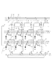
図1は、第1の実施形態を示す模式図である。図1において、画素6は2次元状に8画素配置されている。これら画素が配置された領域を光電変換領域とする。
(First embodiment)
FIG. 1 is a schematic diagram showing the first embodiment. In FIG. 1, 8 pixels are two-dimensionally arranged. A region where these pixels are arranged is a photoelectric conversion region.
1は光電変換素子であり入射光を電荷に変換する。2は転送部であり、光電変換素子の電荷を後述の増幅部の入力部に転送する。転送部としてMOSトランジスタを用いることができる。3は増幅部の入力部である。半導体基板に形成された浮遊拡散領域(フローティングディフュージョン:FD)を用いることができる。4は増幅部の一部であるMOSトランジスタ(増幅MOSトランジスタ)である。ゲートがFDに電気的に接続されている。増幅部は、この増幅MOSトランジスタを含む周知のソースフォロワ回路で構成される。
A
5はFDに電圧を供給するための電圧供給部である。これには、MOSトランジスタを用いることができる。特に、FDの電位を所定値に設定するリセットMOSトランジスタを用いることができる。FDは転送MOSトランジスタ2のドレインを兼ねることができる。そして、FD3,増幅MOSトランジスタ4のゲート、リセットMOSトランジスタ5のソースが接続されている。また、リセットMOSトランジスタ5のドレインは電圧供給線15に、増幅MOSトランジスタ4のソースは出力線16に接続されている。
光電変換領域には、画素を行列状に配置することができる。または、光電変換素子、増幅部、転送部、電圧供給部を行列状に配することもできる。 Pixels can be arranged in a matrix in the photoelectric conversion region. Alternatively, photoelectric conversion elements, amplification units, transfer units, and voltage supply units can be arranged in a matrix.
信号の読み出しシーケンスを説明する。光電変換素子1の電荷が転送部2を介して増幅部の入力部3に転送される。そして、この入力部の電位変化に基づく信号が増幅部4を介して出力線16に読み出されることにより外部に信号を出力する。
A signal reading sequence will be described. The electric charge of the
ここで画素とは、1つの光電変換素子及びこの光電変換素子から出力線へ信号を読み出すための素子集合の最小単位を指す。この素子集合に含まれるのは、転送部2、増幅部4、電圧供給部5である。隣接する光電変換素子において、上記素子を共有することも可能であるが、この場合にも1つの光電変換素子の信号を読み出すための素子集合の最小単位で定義づけられる。
Here, the pixel refers to one photoelectric conversion element and a minimum unit of an element set for reading a signal from the photoelectric conversion element to an output line. The element set includes the
さらに、各列の電圧供給線15にはそれぞれ電圧供給制御回路11が接続されている。電圧供給制御回路11は、ハイレベル(5V)が印加された電源線12、ローレベル(0V)が印加された電源線13、画素電源選択信号線14と共に電源制御部18を構成している。電圧供給制御回路は、電源線と複数の電圧供給部との間の電源供給路中に設けられ、複数の電圧供給部に対する電圧供給を制御しているといえる。なお、電源線12,13、画素電源選択信号線14は複数の電源制御部18で共有することが可能である。
Further, the voltage
電源制御部18の構成例を示したものが図2である。画素電源選択信号線14で伝達されるパルスP_VSELのレベルによって、電源線12と電源線13のどちらかの電源レベルを、インバーター41とCMOSスイッチ42を用いて、電圧供給線15に出力する構成となっている。図2において、P_VSELがハイレベルの時、電圧供給線15にはハイレベル(5V)が印加される。P_VSELがローレベルの時、電圧供給線15にはローレベル(0V)が印加される。電源線12と電源線13には常に電圧が供給されていることが好ましい。一定期間、電圧供給線に電圧を供給しない場合にはその間電圧供給を止めることもできる。以上説明した構成は、後述の実施形態においても適用可能である。
FIG. 2 shows a configuration example of the power
本実施形態は、このような電圧供給制御回路11を各列に設けたことを特徴とする。
The present embodiment is characterized in that such a voltage
以下、図3に示すタイミング模式図を用いて、図1の光電変換装置の動作を説明する。ここで画素の光信号を出力する行、すなわち選択行をn行目の行とし、それ以外の行、すなわち非選択行をn+1行目の行としてn行目の動作を簡単に説明する。 Hereinafter, the operation of the photoelectric conversion device in FIG. 1 will be described with reference to a schematic timing diagram shown in FIG. Here, the operation of the nth row will be briefly described with the row outputting the optical signal of the pixel, that is, the selected row as the nth row and the other row, ie, the non-selected row as the (n + 1) th row.
図3における時刻t0では、電圧供給制御回路11により設定される電圧供給線15の電位は低電位(0V)である。そして、リセットスイッチ制御パルスP_Res(n)、P_Res(n+1)、転送スイッチ制御パルスP_Tx(n)、P_Tx(n+1)、は全てローレベルである。この時、リセットMOSトランジスタ5は非導通状態で、FD3は低電位(0V程度)でフローティング状態となっている。そして、増幅MOSトランジスタ4も非選択状態となるため、出力線16の電位は変化しない。
At time t0 in FIG. 3, the potential of the
次に、時刻t1からt2において、電圧供給線15は各列に設けられた電圧供給制御回路11によって高電位(5V)に設定される。このとき、P_VSELはハイレベルである。ここで、電圧供給線15の各列に電圧供給制御回路11を設けることにより、従来に比べて電圧供給線を充電する時間が短縮できる。これは各電圧制御回路により高電位に設定すべき配線は、各列ごとの電圧供給線15のみのためである。したがって、光電変換領域内すべての電圧供給線を低電位(0V)から高電位(5V)に充電するのにかかる時間が短縮できる。
Next, from time t1 to t2, the
次に、時刻t3からt4において、画素の光信号を出力するn行目のリセットスイッチ制御パルスP_Res(n)をハイレベルとする。この時、リセットMOSトランジスタ5が導通状態となり、FD3が高電位に設定され、増幅MOSトランジスタ4が選択状態となる。これによりn行目の画素に含まれるFDの電位変化によって出力線16の電位が変化する状態、すなわちn行目の画素の選択状態となる。
Next, from time t3 to t4, the n-th row reset switch control pulse P_Res (n) for outputting the pixel optical signal is set to the high level. At this time, the
この後、時刻t5からt6において、n行目の転送スイッチ制御パルスP_Tx(n)をハイレベルとする。この時、転送MOSトランジスタ2が導通状態となり、光電変換素子よりFD3に電荷が転送される。そして、転送電荷の量に応じてFD3の電位が変化し、増幅MOSトランジスタ4を通じて出力線16の電位が変化する。
Thereafter, from time t5 to t6, the transfer switch control pulse P_Tx (n) in the nth row is set to the high level. At this time, the
さらに、n行目の転送スイッチ制御パルスP_Tx(n)をローレベルとした時刻t6からt7の期間中に、水平転送パルスを順次導通状態とし、水平転送スイッチ31を順次導通状態とする。そして水平信号転送線32、出力アンプ33を通じて、出力線16の信号レベルを順次出力する。つまり、複数の出力線から並列に読み出された信号を、順次読み出している。
Further, during the period from time t6 to t7 when the transfer switch control pulse P_Tx (n) in the n-th row is set to the low level, the horizontal transfer pulse is sequentially turned on, and the
さらに、時刻t7からt8において、電圧供給線15の電位を各列に設けられた電圧供給制御回路11によって低電位(0V)とする。ここで、各列の電圧供給線15に電圧供給制御回路11を配置していることにより、従来に比べて電圧供給線を所望の電位に設定する時間が短縮できる。光電変換領域内すべての電圧供給線を所望の電位に設定するのにかかる時間が短縮できる。その後、n+1行の画素の選択動作へと続く。
Further, from time t7 to t8, the potential of the
本実施形態の構成に依れば、各列に電圧供給制御回路11を設けることにより、光電変換領域が大きくなった場合でも電圧供給線の所望の電位に設定する時間を短縮でき、その結果フレームレートを向上させることが可能となる。
According to the configuration of the present embodiment, by providing the voltage
(第2の実施形態)
図4は、第2の実施形態を示す模式図である。本実施形態は、第1の実施の形態と比べて、電圧供給制御回路11の配置が異なる。出力線16に接続される負荷手段である定電流源17と光電変換領域に対して対称となる位置に設けたことを特徴とする。光電変換装置の動作は、第1の実施形態と同様であり、説明を省略する。
(Second Embodiment)
FIG. 4 is a schematic diagram showing the second embodiment. In the present embodiment, the arrangement of the voltage
本実施形態の構成に依れば、各列に電圧供給制御回路11を設けることによるフレームレートの向上が可能になる。これに加え、電圧供給制御回路11が定電流源17の近傍に配置されることによる電源配線どうしのカップリングによる電源振られの影響を抑制することができる。これにより、安定した電圧を電圧供給線15に印加することが可能となる。さらに、光電変換領域の近傍に電圧供給制御回路を配置することが可能となり、配線に生じる寄生抵抗を少なくできるため、電圧降下を抑制することも可能となる。
According to the configuration of the present embodiment, the frame rate can be improved by providing the voltage
(第3の実施形態)
図5は第3の実施形態を示す模式図である。本実施の形態は、第1の実施形態と比べて、電圧供給制御回路11を、各列で光電変換領域に対して交互に対称に設けていることを特徴とする。又は図示はしないが複数列ごとに交互に設けることもできる。光電変換装置の動作は、第1の実施の形態と同様であり、説明を省略する。
(Third embodiment)
FIG. 5 is a schematic diagram showing the third embodiment. Compared with the first embodiment, the present embodiment is characterized in that the voltage
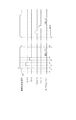
ここで、図6(a)のように電圧供給制御回路11により設定される電圧供給線15の電圧降下について考える。画素6あたりの電圧供給線15の配線抵抗と、電圧供給線15により駆動されるトランジスタのON−OFF抵抗の和をRpixとし、電圧供給線15に流れる電流をIvddとする。図6(b)に示すように、光電変換領域の上端部と下端部では全画素分の電圧降下の和Σ(Ivdd・Rpix)の電位差が発生する。これは、上端部の画素と下端部の画素に同レベルの光が入射した場合、出力される信号にΣ(Ivdd・Rpix)の差が発生することを示す。すなわちシェーディングと呼ばれる現象の原因となる場合がある。
Here, the voltage drop of the
ここで、図7(a)のように上端部にのみ電圧供給制御回路11があり、電圧供給線15の電位を設定している場合を考える。この時、図7(b)に示すように、すべての列において列の上下で出力される信号にΣ(Ivdd・Rpix)の差が発生する。このため、出力全体を見たとき、上下で出力差が有ることがより顕著に確認される。それに対し、図8(a)のように、上端部、下端部交互に電圧供給制御回路11を配置し、電圧供給線15の電位を設定する場合を考える。この場合、各列でΣ(Ivdd・Rpix)の電位差があるのは変わらないが、その方向が偶数列と奇数列で逆方向である。そのため、図8(b)のように、出力全体として見たとき、それぞれのシェーディングが平均化されて視認され、画質が大幅に改善することが可能となる。また、2列ごとに一つの電圧供給制御回路11を配置すればよく、画素サイズが微細になった際でも容易に配置しうる。
Here, consider the case where the voltage
上述のように、本実施の形態の構成に依れば、各列に電圧供給制御回路11があることによるフレームレートの向上に加え、電圧供給線の列方向での電圧降下の差によるシェーディング現象を抑制することが可能となる。そして画素のサイズを縮小化した際にも各素子、回路の配置が容易となる。
As described above, according to the configuration of the present embodiment, in addition to the improvement in frame rate due to the presence of the voltage
(第4の実施形態)
図9は第4の実施形態を示す模式図である。本実施形態は、第1の実施の形態と比べて、電圧供給制御回路11を、各列に光電変換領域を挟んで対向位置両方に設けていることを特徴とする。光電変換装置の動作は、第1の実施形態と同様であり説明を省略する。
(Fourth embodiment)
FIG. 9 is a schematic diagram showing the fourth embodiment. Compared with the first embodiment, the present embodiment is characterized in that the voltage
ここで、図10(a)のように電圧供給制御回路11により設定される電圧供給線15の電圧の時間変化について考える。単位画素6あたりの電圧供給線15の配線抵抗と、電圧供給線15により駆動されるトランジスタのON−OFF抵抗の和をRpixとする。そして、単位画素6あたりの電圧供給線15の配線容量と、電圧供給線15により駆動されるトランジスタのゲート容量の和をCpixとする。この場合、図10(b)に示すように、電圧供給線15の電位は時間変化する。ただし、図10(b)の時刻t0で電圧供給線15が充電されはじめ、時刻t1で充電完了、時刻t2で放電されはじめ、時刻t3で放電完了となっているとする。この時、t0からt1の時間とt2からt3の時間は電圧供給線15のRC時定数であるRpixとCpixの積に比例する。
Here, consider the time change of the voltage of the
これに対し、図11(a)のように電圧供給線15を対向する両端より電圧を供給する場合を考えると、図10(a)のRpixとCpixがそれぞれ半分になったものと等価となる。この時、図11(b)の時刻t0で電圧供給線15が充電されはじめ、時刻t1’で充電完了、時刻t2で放電されはじめ、時刻t3’で放電完了となっているとする。t0からt1’の時間とt2からt3’の時間は、電圧供給線15のRC時定数は、Rpix/2とCpix/2の積に比例するため、図10(b)の場合の1/4の時間で電位が設定される。
On the other hand, when a voltage is supplied from both ends facing the
また、電圧供給線15を両側から電位を設定することにより、電圧降下は中央部で大きくなるが、シェーディング量の絶対値としては、図11(c)のように片側から駆動する場合の1/2で抑えられる。
In addition, by setting the potential of the
上述のように、本実施形態の構成に依れば、各列に電圧供給制御回路11があることによるフレームレートの向上に加え、より高速で電位設定可能になるため更にフレームレートを向上することができる。さらに、電圧供給線の列方向での電圧降下の差によるシェーディング現象を抑制することが可能となる。
As described above, according to the configuration of the present embodiment, in addition to the improvement of the frame rate due to the presence of the voltage
(第5の実施形態)
図12は第5の実施形態を示す模式図である。本実施形態は、第1の実施形態と比べて異なる点は光電変換領域からの信号の読み出し方である。光電変換領域からの出力が上下複数のチャネルに読み出されるようになっている。光電変換装置の動作は、第1の実施の形態と同様であり、説明を省略する。
(Fifth embodiment)
FIG. 12 is a schematic diagram showing the fifth embodiment. This embodiment is different from the first embodiment in how to read a signal from the photoelectric conversion region. The output from the photoelectric conversion region is read out to a plurality of upper and lower channels. The operation of the photoelectric conversion device is the same as that of the first embodiment, and a description thereof is omitted.
電圧供給線15の各列に電圧供給制御回路11を設けることにより、電圧供給線の電位を設定する時間が短縮でき、光電変換領域内すべての電圧供給線の電位を設定するのにかかる時間が短縮できる。
By providing the voltage
また各列に電圧供給制御回路11を設けることにより、光電変換領域が大きくなった場合でも電圧供給線の電位設定にかかる時間を短縮できる。上下複数チャネルで出力する光電変換装置においても、フレームレートを向上させることが可能となる。
Further, by providing the voltage
(第6の実施の形態)
図13は本発明の第6の実施形態を示す模式図である。本実施の形態は、第5の実施の形態と比べて電圧供給制御回路の配置が異なる。電圧供給制御回路11を、各列で光電変換領域を挟んで対向する位置に交互に対称に設けていることを特徴とする。または図示はしないが、複数列ごとに交互に設けることもできる。光電変換装置の動作は、第1の実施形態と同様であり、説明を省略する。
(Sixth embodiment)
FIG. 13 is a schematic view showing a sixth embodiment of the present invention. This embodiment differs from the fifth embodiment in the arrangement of the voltage supply control circuit. The voltage
本実施の形態の構成に依れば、各列に電圧供給制御回路11を設けることによるフレームレートが向上する。また、光電変換領域の上端部からと、下端部からと交互にシェーディングの方向が変わる。したがって、出力全体として見たとき、それぞれのシェーディングが平均化されて視認され、画質が大幅に改善することが可能となる。また回路の配置も容易となるため、画素サイズ縮小時にも有用である。
According to the configuration of the present embodiment, the frame rate is improved by providing the voltage
(第7の実施の形態)
図14は本発明の第7の実施形態を示す模式図である。本実施形態は、第5の実施の形態と比べて異なるのは、電圧供給制御回路と定電流源の配置関係である。電圧供給制御回路11を、出力線16に接続される負荷手段である定電流源17と光電変換領域を挟んで対向する位置に設けている。そして各列で画素に対して交互に対称に設けていることを特徴とする。図示はしないが複数列ごとに交互に設けることもできる。光電変換装置の動作は、第1の実施の形態と同様であり、説明を省略する。
(Seventh embodiment)
FIG. 14 is a schematic view showing a seventh embodiment of the present invention. This embodiment is different from the fifth embodiment in the arrangement relationship between the voltage supply control circuit and the constant current source. The voltage
本実施の形態の構成に依れば、各列に電圧供給制御回路11があることによるフレームレートが向上する。更に光電変換領域の近傍に電圧供給制御回路11を配置することが可能となり、配線に生じる寄生抵抗を少なくできる。そのため、電圧降下を抑制することも可能となる。また、定電流源17の配置されない側に電圧供給制御回路11を配置し、電圧供給制御回路11の配置されない側に低電流源17を配置する構成となっている。したがって、2列あたり、電圧供給制御回路11と定電流源17を一つずつ配置する構成となる。このため、回路の配置上無駄になるスペースが小さく、微細化に好適である。さらに、画素に対して各列で対称的な構造をとるため、光学的なレイアウトの対称性もよい。
According to the configuration of the present embodiment, the frame rate due to the voltage
(第8の実施形態)
図15は第8の実施形態を示す模式図である。本実施形態は、第5の実施形態と比べて電圧供給制御回路の構成が異なる。電圧供給制御回路11を、各列で画素に対して上下両方に設けていることを特徴とする。光電変換装置の動作は、第1の実施の形態と同様であり、説明を省略する。
(Eighth embodiment)
FIG. 15 is a schematic diagram showing the eighth embodiment. This embodiment differs from the fifth embodiment in the configuration of the voltage supply control circuit. The voltage
本実施の形態の構成に依れば、各列に電圧供給制御回路11を設けることによるフレームレートが向上する。また、光電変換領域を挟んで対向する位置、つまり列方向の両端部から電圧供給線の電位を設定することが可能になる。これにより時定数を小さくでき、さらにフレームレートを向上することができる。また、電圧供給線の列方向での電圧降下の差によるシェーディング現象を抑制することが可能となる。
According to the configuration of the present embodiment, the frame rate is improved by providing the voltage
(第9の実施形態)
図16は第9の実施形態を示す模式図である。本実施形態は、第8の実施の形態と比べて電圧供給線の構成が異なる。リセットMOSトランジスタのドレインに電圧を供給する電圧供給線を出力線と兼ねた構成としている。増幅MOSトランジスタのドレインに電圧を供給する配線は、これとは別にVDDの固定電圧を供給している。さらに電圧供給制御回路に印加される電源電圧がそれぞれ設定可能となっている。
(Ninth embodiment)
FIG. 16 is a schematic diagram showing the ninth embodiment. This embodiment is different from the eighth embodiment in the configuration of the voltage supply line. A voltage supply line for supplying a voltage to the drain of the reset MOS transistor also serves as an output line. Separately from this, the wiring for supplying a voltage to the drain of the amplification MOS transistor supplies a fixed voltage of VDD. Further, the power supply voltage applied to the voltage supply control circuit can be set respectively.
図17に示すタイミング模式図を用いて、図17の光電変換装置の動作を説明する。ここで画素の光信号を出力する行、すなわち選択行をn行目の行とし、それ以外の行、すなわち非選択行をn+1行目の行としてn行目の動作を簡単に説明する。 The operation of the photoelectric conversion device in FIG. 17 will be described with reference to a schematic timing diagram shown in FIG. Here, the operation of the nth row will be briefly described with the row outputting the optical signal of the pixel, that is, the selected row as the nth row and the other row, ie, the non-selected row as the (n + 1) th row.
図17における時刻t0では、電圧供給制御回路11により設定される出力線16の電位は低電位(0V)である。そして、リセットスイッチ制御パルスP_Res(n)、P_Res(n+1)、転送スイッチ制御パルスP_Tx(n)、P_Tx(n+1)は全てローレベルとなっている。この時、リセットMOSトランジスタ5は非導通状態で、FD3は低電位(0V程度)でフローティング状態となっている。増幅MOSトランジスタ4も非選択状態となるため、出力線16の電位は変化しない。
At time t0 in FIG. 17, the potential of the
次に、時刻t1からt2において、電圧供給線として機能する配線16の電位は各列に設けられた電圧供給制御回路11によって、高電位(5V)に設定される。ここで、配線16の各列に電圧供給制御回路11を配置することにより、配線16の電位を設定する時間が短縮でき、光電変換領域内すべての配線16を低電位(0V)から高電位(5V)に設定するのにかかる時間が短縮できる。
Next, from time t1 to t2, the potential of the
次に、時刻t3からt4において、画素の光信号を出力するn行目のリセットスイッチ制御パルスP_Res(n)をハイレベルとする。この時、リセットMOSトランジスタ5が導通状態となり、FD3が高電位に設定される。
Next, from time t3 to t4, the n-th row reset switch control pulse P_Res (n) for outputting the pixel optical signal is set to the high level. At this time, the
次に、リセットスイッチ制御パルスP_Res(n)をローレベルとして、電圧供給制御回路11をOFF状態とし、定電流源17をON状態とすると、増幅MOSトランジスタ4が選択状態となる。これにより、n行目の画素に含まれるFDの電位変動によって配線16の電位が変化する状態、すなわちn行目の画素の選択状態となる。
Next, when the reset switch control pulse P_Res (n) is set to a low level, the voltage
この後、時刻t5からt6において、n行目の転送スイッチ制御パルスP_Tx(n)をハイレベルとする。この時、転送MOSトランジスタ2が導通状態となり、光電変換素子よりFDに電荷が転送され、転送電荷の量に応じてFDの電位が変化し、増幅MOSトランジスタを通じて、出力線16の電位が変化する。
Thereafter, from time t5 to t6, the transfer switch control pulse P_Tx (n) in the nth row is set to the high level. At this time, the
さらに、n行目の転送スイッチ制御パルスP_Tx(n)をローレベルとした時刻t6からt7の期間中に、水平転送パルスを順次導通状態とし、水平転送スイッチ31を順次導通状態とする。これにより、水平信号転送線32、出力アンプ33を通じて、配線16の信号レベルを順次出力する。
Further, during the period from time t6 to t7 when the transfer switch control pulse P_Tx (n) in the n-th row is set to the low level, the horizontal transfer pulse is sequentially turned on, and the
さらに、時刻t7からt8において、配線16の電位を各列に設けられた電圧供給制御回路11によって、低電位(0V)に設定する。ここで、配線16の各列に電圧供給制御回路11を配置していることにより、配線16の電位を設定する時間が短縮でき、結果、光電変換領域内すべての配線16の電位を設定するのにかかる時間が短縮できる。その後、n+1行の画素の選択動作へと続く。
Further, from time t7 to t8, the potential of the
本実施の形態の構成に依れば、各列に電圧供給制御回路11を設けることにより、光電変換領域が大きくなった場合でも配線16の電位の設定にかかる時間を短縮でき、結果フレームレートを向上させることが可能となる。さらに、電圧供給制御回路11を画素の列方向両側に配置することで配線16の電位の設定を両側から行なうことが可能になり時定数を小さくでき、さらにフレームレートを向上することができる。また、配線16の列方向での電圧降下の差によるシェーディング現象を抑制することが可能となる。さらに、各電圧供給制御回路に印加される電源電圧がそれぞれ設定可能となっている。これにより、MOSトランジスタの閾値の変動などで列ごとにオフセットなどが重畳された場合に、それをキャンセルする電圧設定が可能となる。すなわち列ごとの固定パタンノイズの除去も可能となる。
According to the configuration of the present embodiment, by providing the voltage
以上説明したように、本発明の光電変換装置に依れば、フレームレートの向上が可能となる。更に、各実施形態の構成によればシェーディング現象の抑制、高画素数化、画素サイズの微細化等の少なくともいずれか1つが可能となる。 As described above, according to the photoelectric conversion device of the present invention, the frame rate can be improved. Furthermore, according to the configuration of each embodiment, at least one of suppression of shading phenomenon, increase in the number of pixels, miniaturization of pixel size, and the like can be performed.
なお、図2において電源制御部18の構成例を示したが、これに限定するものではなく、制御する配線の電圧レベルを切り替える手段をもつ構成であれば、図2の構成を取らなくてもよい。
Although the configuration example of the power
また、電圧供給制御回路、定電流源は光電変換領域外に配される。この模式図を図18に示す。1801が光電変換領域、1804,1805が電圧供給制御回路、定電流源の少なくとも一方が配される領域である。1804,1805は光電変換領域を挟んで対向する位置に配されているといえる。また1806は1804,1805への電源供給、パルス信号供給を行なう制御部である。これは走査回路1802、1803の制御を行なうこともできる。1803から信号が出力される。ここでは各領域、回路間をつなぐ配線を一部省略している。
The voltage supply control circuit and the constant current source are arranged outside the photoelectric conversion region. This schematic diagram is shown in FIG.
また、0V、5Vの2種類の電圧レベルを切り替える構成を説明したが、電圧レベルを上記2種類のみに限定するものではなく、それ以外の電圧や、3種類以上の電圧レベルを切り替える構成も取りうる。 In addition, the configuration for switching between two voltage levels of 0V and 5V has been described, but the voltage level is not limited to the above two types, and other voltages and a configuration for switching between three or more types of voltage levels can also be used. sell.
(光電変換装置を用いた撮像システム)
図19は、本発明による固体撮像装置をカメラに応用する場合の回路ブロックの例を示したものである。撮影レンズ1002の手前にはシャッター1001があり、露出を制御する。絞り1003により必要に応じ光量を制御し、固体撮像装置1004に結像させる。固体撮像装置1004から出力された信号は信号処理回路1005で処理され、A/D変換器1006によりアナログ信号からディジタル信号に変換される。出力されるディジタル信号はさらに信号処理部1007で演算処理される。処理されたディジタル信号はメモリ1010に蓄えられたり、外部I/F1013を通して外部の機器に送られる。固体撮像装置1004、撮像信号処理回路1005、A/D変換器1006、信号処理部1007はタイミング発生部1008により制御される他、システム全体は全体制御部・演算部1009で制御される。記録媒体1012に画像を記録するために、出力ディジタル信号は全体制御部・演算部で制御される記録媒体制御I/F部1011を通して、記録される。
(Imaging system using photoelectric conversion device)
FIG. 19 shows an example of a circuit block when the solid-state imaging device according to the present invention is applied to a camera. A
1 光電変換素子
2 転送部
3 増幅部の入力部
4 増幅MOSトランジスタ
5 リセットMOSトランジスタ
6 画素
11 電圧供給制御回路
12 電源線(画素電源ハイレベル)
13 電源線(画素電源ローレベル)
14 画素電源選択信号線
15 電圧供給線
16 出力線
17 定電流源
18 電源制御部
41 インバーター
42 CMOSスイッチ
DESCRIPTION OF
13 Power supply line (Pixel power supply low level)
14 pixel power supply
Claims (10)
前記光電変換素子の電荷に基づく信号を出力線に読み出す増幅部と、
前記光電変換素子の電荷を前記増幅部の入力部に転送する転送部と、
前記入力部の電位を少なくとも第1及び第2の電位に設定するための電圧を前記入力部に供給する電圧供給部と、が2次元状に配された光電変換領域を有する光電変換装置であって、
前記電圧供給部に電圧を供給するための電源線を有し、前記電源線と複数の前記電圧供給部との間の電源供給路中に、複数の前記電圧供給部に対する電圧供給を制御する電圧供給制御回路を複数有し、
前記電源線が、第1の電圧を供給する第1の電源線と、前記第1の電圧よりも小さい第2の電圧を供給する第2の電源線と、
を有し、
前記光電変換装置は、更に、前記第1、第2の電圧の切り替えを制御するためのパルスを供給する選択線を有し、
前記複数の電圧供給制御回路の各々が、前記選択線から供給されるパルスを受けることを特徴とする光電変換装置。 A photoelectric conversion element that converts incident light into electric charge;
An amplifier for reading out a signal based on the charge of the photoelectric conversion element to an output line;
A transfer unit that transfers the charge of the photoelectric conversion element to the input unit of the amplification unit;
A voltage supply unit that supplies the input unit with a voltage for setting the potential of the input unit to at least the first and second potentials, and a photoelectric conversion device having a photoelectric conversion region arranged two-dimensionally. And
A voltage having a power supply line for supplying a voltage to the voltage supply section, and controlling voltage supply to the plurality of voltage supply sections in a power supply path between the power supply line and the plurality of voltage supply sections. Have multiple supply control circuits ,
A first power supply line for supplying a first voltage; a second power supply line for supplying a second voltage lower than the first voltage;
Have
The photoelectric conversion device further includes a selection line for supplying a pulse for controlling switching of the first and second voltages.
Each of the plurality of voltage supply control circuits receives a pulse supplied from the selection line .
Priority Applications (5)
| Application Number | Priority Date | Filing Date | Title |
|---|---|---|---|
| JP2006209755A JP4818018B2 (en) | 2006-08-01 | 2006-08-01 | Photoelectric conversion device and imaging system using the same |
| EP07111739.4A EP1885117B1 (en) | 2006-08-01 | 2007-07-04 | Photoelectric conversion apparatus and image pickup system using photoelectric conversion apparatus |
| US11/774,262 US7462810B2 (en) | 2006-08-01 | 2007-07-06 | Photoelectric conversion apparatus and image pickup system using photoelectric conversion apparatus |
| CN2007101383824A CN101119447B (en) | 2006-08-01 | 2007-08-01 | Photoelectric conversion apparatus and image pickup system using photoelectric conversion apparatus |
| US12/259,355 US8063351B2 (en) | 2006-08-01 | 2008-10-28 | Photoelectric conversion apparatus and image pickup system using photoelectric conversion apparatus |
Applications Claiming Priority (1)
| Application Number | Priority Date | Filing Date | Title |
|---|---|---|---|
| JP2006209755A JP4818018B2 (en) | 2006-08-01 | 2006-08-01 | Photoelectric conversion device and imaging system using the same |
Publications (2)
| Publication Number | Publication Date |
|---|---|
| JP2008042239A JP2008042239A (en) | 2008-02-21 |
| JP4818018B2 true JP4818018B2 (en) | 2011-11-16 |
Family
ID=38530574
Family Applications (1)
| Application Number | Title | Priority Date | Filing Date |
|---|---|---|---|
| JP2006209755A Expired - Fee Related JP4818018B2 (en) | 2006-08-01 | 2006-08-01 | Photoelectric conversion device and imaging system using the same |
Country Status (4)
| Country | Link |
|---|---|
| US (2) | US7462810B2 (en) |
| EP (1) | EP1885117B1 (en) |
| JP (1) | JP4818018B2 (en) |
| CN (1) | CN101119447B (en) |
Families Citing this family (66)
| Publication number | Priority date | Publication date | Assignee | Title |
|---|---|---|---|---|
| JP5132102B2 (en) * | 2006-08-01 | 2013-01-30 | キヤノン株式会社 | Photoelectric conversion device and imaging system using photoelectric conversion device |
| JP5110820B2 (en) * | 2006-08-02 | 2012-12-26 | キヤノン株式会社 | Photoelectric conversion device, photoelectric conversion device manufacturing method, and imaging system |
| JP4185949B2 (en) * | 2006-08-08 | 2008-11-26 | キヤノン株式会社 | Photoelectric conversion device and imaging device |
| JP4979375B2 (en) * | 2006-12-28 | 2012-07-18 | キヤノン株式会社 | Solid-state imaging device and imaging system |
| JP2009021809A (en) * | 2007-07-11 | 2009-01-29 | Canon Inc | Driving method of imaging device, imaging device, and imaging system |
| JP2009077098A (en) * | 2007-09-20 | 2009-04-09 | Sony Corp | Solid-state imaging element and drive system thereof |
| JP5164531B2 (en) | 2007-11-13 | 2013-03-21 | キヤノン株式会社 | Solid-state imaging device |
| JP5366396B2 (en) * | 2007-12-28 | 2013-12-11 | キヤノン株式会社 | Photoelectric conversion device manufacturing method, semiconductor device manufacturing method, photoelectric conversion device, and imaging system |
| JP5014114B2 (en) * | 2007-12-28 | 2012-08-29 | キヤノン株式会社 | Imaging apparatus and imaging system |
| JP4685120B2 (en) | 2008-02-13 | 2011-05-18 | キヤノン株式会社 | Photoelectric conversion device and imaging system |
| JP5371463B2 (en) | 2008-02-28 | 2013-12-18 | キヤノン株式会社 | IMAGING DEVICE, IMAGING SYSTEM, AND IMAGING DEVICE CONTROL METHOD |
| JP5213501B2 (en) * | 2008-04-09 | 2013-06-19 | キヤノン株式会社 | Solid-state imaging device |
| JP4494492B2 (en) * | 2008-04-09 | 2010-06-30 | キヤノン株式会社 | Solid-state imaging device and driving method of solid-state imaging device |
| JP4759590B2 (en) * | 2008-05-09 | 2011-08-31 | キヤノン株式会社 | Photoelectric conversion device and imaging system using the same |
| JP5102115B2 (en) * | 2008-06-05 | 2012-12-19 | キヤノン株式会社 | Imaging apparatus and imaging system |
| JP5279352B2 (en) | 2008-06-06 | 2013-09-04 | キヤノン株式会社 | Solid-state imaging device |
| JP4650572B2 (en) * | 2009-01-20 | 2011-03-16 | ソニー株式会社 | Image sensor, control method therefor, and camera |
| JP5226591B2 (en) * | 2009-04-09 | 2013-07-03 | オリンパス株式会社 | Solid-state imaging device and camera system |
| JP2010268080A (en) | 2009-05-12 | 2010-11-25 | Canon Inc | Solid-state imaging apparatus |
| JP2011004390A (en) | 2009-05-18 | 2011-01-06 | Canon Inc | Imaging device, imaging system, and method for driving imaging device |
| JP5762199B2 (en) | 2011-07-28 | 2015-08-12 | キヤノン株式会社 | Solid-state imaging device |
| JP5901186B2 (en) | 2011-09-05 | 2016-04-06 | キヤノン株式会社 | Solid-state imaging device and driving method thereof |
| JP5858695B2 (en) | 2011-09-08 | 2016-02-10 | キヤノン株式会社 | Solid-state imaging device and driving method of solid-state imaging device |
| JP5806566B2 (en) | 2011-09-15 | 2015-11-10 | キヤノン株式会社 | A / D converter and solid-state imaging device |
| JP5801665B2 (en) | 2011-09-15 | 2015-10-28 | キヤノン株式会社 | Solid-state imaging device, A / D converter and control method thereof |
| JP2013093553A (en) | 2011-10-04 | 2013-05-16 | Canon Inc | Photoelectric conversion device and manufacturing method therefor, and photoelectric conversion system |
| JP5484422B2 (en) | 2011-10-07 | 2014-05-07 | キヤノン株式会社 | Solid-state imaging device |
| JP5901212B2 (en) | 2011-10-07 | 2016-04-06 | キヤノン株式会社 | Photoelectric conversion system |
| JP5930651B2 (en) | 2011-10-07 | 2016-06-08 | キヤノン株式会社 | Solid-state imaging device |
| JP6053505B2 (en) | 2012-01-18 | 2016-12-27 | キヤノン株式会社 | Solid-state imaging device |
| JP5967944B2 (en) | 2012-01-18 | 2016-08-10 | キヤノン株式会社 | Solid-state imaging device and camera |
| JP5886806B2 (en) | 2013-09-17 | 2016-03-16 | キヤノン株式会社 | Solid-state imaging device |
| JP6245997B2 (en) | 2014-01-16 | 2017-12-13 | キヤノン株式会社 | Solid-state imaging device and imaging system |
| JP6261361B2 (en) | 2014-02-04 | 2018-01-17 | キヤノン株式会社 | Solid-state imaging device and camera |
| JP6057931B2 (en) | 2014-02-10 | 2017-01-11 | キヤノン株式会社 | Photoelectric conversion device and imaging system using the same |
| JP6274567B2 (en) | 2014-03-14 | 2018-02-07 | キヤノン株式会社 | Solid-state imaging device and imaging system |
| JP6595750B2 (en) | 2014-03-14 | 2019-10-23 | キヤノン株式会社 | Solid-state imaging device and imaging system |
| JP6541347B2 (en) | 2014-03-27 | 2019-07-10 | キヤノン株式会社 | Solid-state imaging device and imaging system |
| JP6417197B2 (en) | 2014-11-27 | 2018-10-31 | キヤノン株式会社 | Solid-state imaging device |
| JP6541523B2 (en) | 2015-09-11 | 2019-07-10 | キヤノン株式会社 | Imaging device, imaging system, and control method of imaging device |
| US10205894B2 (en) | 2015-09-11 | 2019-02-12 | Canon Kabushiki Kaisha | Imaging device and imaging system |
| JP6570384B2 (en) | 2015-09-11 | 2019-09-04 | キヤノン株式会社 | Imaging apparatus and imaging system |
| KR102686510B1 (en) | 2016-06-08 | 2024-07-19 | 소니그룹주식회사 | Solid-state imaging device, imaging device, and control method of solid-state imaging device |
| JP6776011B2 (en) | 2016-06-10 | 2020-10-28 | キヤノン株式会社 | Imaging device and imaging system |
| JP6688165B2 (en) | 2016-06-10 | 2020-04-28 | キヤノン株式会社 | Imaging device and imaging system |
| JP6727938B2 (en) | 2016-06-10 | 2020-07-22 | キヤノン株式会社 | IMAGING DEVICE, IMAGING DEVICE CONTROL METHOD, AND IMAGING SYSTEM |
| JP7013119B2 (en) | 2016-07-21 | 2022-01-31 | キヤノン株式会社 | Solid-state image sensor, manufacturing method of solid-state image sensor, and image pickup system |
| JP6436953B2 (en) | 2016-09-30 | 2018-12-12 | キヤノン株式会社 | Solid-state imaging device, driving method thereof, and imaging system |
| JP2018092976A (en) | 2016-11-30 | 2018-06-14 | キヤノン株式会社 | Imaging apparatus |
| JP6552478B2 (en) | 2016-12-28 | 2019-07-31 | キヤノン株式会社 | Solid-state imaging device |
| US10652531B2 (en) | 2017-01-25 | 2020-05-12 | Canon Kabushiki Kaisha | Solid-state imaging device, imaging system, and movable object |
| JP6957157B2 (en) | 2017-01-26 | 2021-11-02 | キヤノン株式会社 | Solid-state image sensor, image sensor, and method for manufacturing solid-state image sensor |
| JP6701108B2 (en) | 2017-03-21 | 2020-05-27 | キヤノン株式会社 | Solid-state imaging device and imaging system |
| JP6929114B2 (en) | 2017-04-24 | 2021-09-01 | キヤノン株式会社 | Photoelectric conversion device and imaging system |
| US10818715B2 (en) | 2017-06-26 | 2020-10-27 | Canon Kabushiki Kaisha | Solid state imaging device and manufacturing method thereof |
| JP6904119B2 (en) * | 2017-07-06 | 2021-07-14 | 株式会社リコー | Solid-state image sensor and image sensor |
| JP6987562B2 (en) | 2017-07-28 | 2022-01-05 | キヤノン株式会社 | Solid-state image sensor |
| JP2019087939A (en) | 2017-11-09 | 2019-06-06 | キヤノン株式会社 | Photoelectric conversion device, electronic equipment, conveyance apparatus and drive method of photoelectric conversion device |
| JP6704893B2 (en) | 2017-11-30 | 2020-06-03 | キヤノン株式会社 | Solid-state imaging device, imaging system, and method for driving solid-state imaging device |
| JP7091080B2 (en) | 2018-02-05 | 2022-06-27 | キヤノン株式会社 | Equipment, systems, and mobiles |
| JP7161317B2 (en) | 2018-06-14 | 2022-10-26 | キヤノン株式会社 | IMAGING DEVICE, IMAGING SYSTEM AND MOVING OBJECT |
| JP7237622B2 (en) | 2019-02-05 | 2023-03-13 | キヤノン株式会社 | Photoelectric conversion device |
| JP7374639B2 (en) | 2019-07-19 | 2023-11-07 | キヤノン株式会社 | Photoelectric conversion device and imaging system |
| JP7303682B2 (en) | 2019-07-19 | 2023-07-05 | キヤノン株式会社 | Photoelectric conversion device and imaging system |
| JP7504623B2 (en) | 2020-02-28 | 2024-06-24 | キヤノン株式会社 | Imaging device and imaging system |
| JP2022119634A (en) | 2021-02-04 | 2022-08-17 | キヤノン株式会社 | Photoelectric conversion device, photoelectric conversion system, mobile body, and semiconductor substrate |
Family Cites Families (26)
| Publication number | Priority date | Publication date | Assignee | Title |
|---|---|---|---|---|
| JPH11103418A (en) | 1997-09-29 | 1999-04-13 | Canon Inc | Photoelectric converting device |
| JP4200545B2 (en) | 1998-06-08 | 2008-12-24 | ソニー株式会社 | Solid-state imaging device, driving method thereof, and camera system |
| JP4809537B2 (en) * | 2000-04-05 | 2011-11-09 | 富士フイルム株式会社 | Imaging control apparatus and imaging control method |
| FR2817106B1 (en) * | 2000-11-17 | 2003-03-07 | Trixell Sas | PHOTOSENSITIVE DEVICE AND METHOD FOR CONTROLLING THE PHOTOSENSITIVE DEVICE |
| US6797933B1 (en) * | 2001-06-29 | 2004-09-28 | Vanguard International Semiconductor Corporation | On-chip design-for-testing structure for CMOS APS (active pixel sensor) image sensor |
| AU2002351116A1 (en) * | 2001-12-21 | 2003-07-09 | Koninklijke Philips Electronics N.V. | Image pick-up device and camera system comprising an image pick-up device |
| JP3940618B2 (en) * | 2002-03-01 | 2007-07-04 | 株式会社東芝 | Solid-state imaging device |
| JP3840214B2 (en) | 2003-01-06 | 2006-11-01 | キヤノン株式会社 | Photoelectric conversion device, method for manufacturing photoelectric conversion device, and camera using the same |
| JP4336508B2 (en) | 2003-03-06 | 2009-09-30 | キヤノン株式会社 | Imaging device |
| JP3794637B2 (en) * | 2003-03-07 | 2006-07-05 | 松下電器産業株式会社 | Solid-state imaging device |
| US7408577B2 (en) * | 2003-04-09 | 2008-08-05 | Micron Technology, Inc. | Biasing scheme for large format CMOS active pixel sensors |
| JP4297416B2 (en) | 2003-06-10 | 2009-07-15 | シャープ株式会社 | Solid-state imaging device, driving method thereof and camera |
| JP2005260790A (en) * | 2004-03-15 | 2005-09-22 | Sony Corp | Solid-state image pickup device and driving method therefor |
| DE602004017969D1 (en) * | 2004-06-05 | 2009-01-08 | St Microelectronics Res & Dev | Image sensor with split reset signals and line selection |
| JP4434844B2 (en) * | 2004-06-08 | 2010-03-17 | オリンパス株式会社 | Solid-state imaging device |
| JP4979195B2 (en) * | 2005-02-21 | 2012-07-18 | ソニー株式会社 | Solid-state imaging device, solid-state imaging device driving method, and imaging apparatus |
| JP4794877B2 (en) | 2005-03-18 | 2011-10-19 | キヤノン株式会社 | Solid-state imaging device and camera |
| JP4677258B2 (en) | 2005-03-18 | 2011-04-27 | キヤノン株式会社 | Solid-state imaging device and camera |
| JP4459099B2 (en) | 2005-03-18 | 2010-04-28 | キヤノン株式会社 | Solid-state imaging device and camera |
| JP4459098B2 (en) | 2005-03-18 | 2010-04-28 | キヤノン株式会社 | Solid-state imaging device and camera |
| JP4862473B2 (en) * | 2005-10-28 | 2012-01-25 | ソニー株式会社 | Solid-state imaging device, driving method of solid-state imaging device, and imaging device |
| JP4898522B2 (en) * | 2006-04-21 | 2012-03-14 | キヤノン株式会社 | Imaging apparatus, radiation imaging system, and imaging apparatus control method |
| JP4956084B2 (en) | 2006-08-01 | 2012-06-20 | キヤノン株式会社 | Photoelectric conversion device and imaging system using the same |
| JP5132102B2 (en) | 2006-08-01 | 2013-01-30 | キヤノン株式会社 | Photoelectric conversion device and imaging system using photoelectric conversion device |
| JP5110820B2 (en) | 2006-08-02 | 2012-12-26 | キヤノン株式会社 | Photoelectric conversion device, photoelectric conversion device manufacturing method, and imaging system |
| JP4979375B2 (en) | 2006-12-28 | 2012-07-18 | キヤノン株式会社 | Solid-state imaging device and imaging system |
-
2006
- 2006-08-01 JP JP2006209755A patent/JP4818018B2/en not_active Expired - Fee Related
-
2007
- 2007-07-04 EP EP07111739.4A patent/EP1885117B1/en not_active Not-in-force
- 2007-07-06 US US11/774,262 patent/US7462810B2/en active Active
- 2007-08-01 CN CN2007101383824A patent/CN101119447B/en not_active Expired - Fee Related
-
2008
- 2008-10-28 US US12/259,355 patent/US8063351B2/en not_active Expired - Fee Related
Also Published As
| Publication number | Publication date |
|---|---|
| US8063351B2 (en) | 2011-11-22 |
| US7462810B2 (en) | 2008-12-09 |
| CN101119447B (en) | 2011-06-01 |
| EP1885117B1 (en) | 2016-09-07 |
| US20080029689A1 (en) | 2008-02-07 |
| EP1885117A3 (en) | 2011-12-07 |
| EP1885117A2 (en) | 2008-02-06 |
| JP2008042239A (en) | 2008-02-21 |
| CN101119447A (en) | 2008-02-06 |
| US20090050787A1 (en) | 2009-02-26 |
Similar Documents
| Publication | Publication Date | Title |
|---|---|---|
| JP4818018B2 (en) | Photoelectric conversion device and imaging system using the same | |
| US10129444B2 (en) | Solid-state imaging element and camera system | |
| US8023025B2 (en) | Photoelectric conversion apparatus and image pickup system using the same | |
| JP4792934B2 (en) | Physical information acquisition method and physical information acquisition device | |
| US8289431B2 (en) | Image sensing device and image sensing system | |
| US8159573B2 (en) | Photoelectric conversion device and imaging system | |
| US10658404B2 (en) | Solid state imaging device and imaging apparatus with pixel column having multiple output lines | |
| KR102553988B1 (en) | Solid-state imaging element, and imaging device | |
| US20140240565A1 (en) | Solid-state imaging device and electronic apparatus | |
| JP2008218648A (en) | Photographing device, and camera | |
| JP5436173B2 (en) | Solid-state imaging device | |
| JP2016019137A (en) | Solid-state imaging device and driving method therefor | |
| JP2015159463A (en) | Solid state imaging device and imaging system | |
| JP4661212B2 (en) | Physical information acquisition method, physical information acquisition device, and semiconductor device | |
| JP2008005155A (en) | Amplified solid-state imaging apparatus, its driving method, and electronic information device | |
| JP2016111376A (en) | Imaging apparatus, imaging system, and imaging apparatus driving method | |
| JP2006210468A (en) | Solid state imaging device | |
| JP2006019343A (en) | Solid-state imaging device | |
| JP6602407B2 (en) | Solid-state imaging device and imaging system | |
| JP5177198B2 (en) | Physical information acquisition method and physical information acquisition device | |
| JP2020102816A (en) | Imaging apparatus and method of controlling imaging apparatus | |
| JP4696788B2 (en) | Solid-state imaging device | |
| JP4241692B2 (en) | Scanning circuit for photoelectric conversion device | |
| JP2020005131A (en) | Solid state image pickup device and imaging system | |
| JP5197440B2 (en) | Photoelectric conversion device |
Legal Events
| Date | Code | Title | Description |
|---|---|---|---|
| A621 | Written request for application examination |
Free format text: JAPANESE INTERMEDIATE CODE: A621 Effective date: 20090731 |
|
| RD04 | Notification of resignation of power of attorney |
Free format text: JAPANESE INTERMEDIATE CODE: A7424 Effective date: 20100201 |
|
| RD01 | Notification of change of attorney |
Free format text: JAPANESE INTERMEDIATE CODE: A7421 Effective date: 20100630 |
|
| A977 | Report on retrieval |
Free format text: JAPANESE INTERMEDIATE CODE: A971007 Effective date: 20110222 |
|
| A131 | Notification of reasons for refusal |
Free format text: JAPANESE INTERMEDIATE CODE: A131 Effective date: 20110301 |
|
| A521 | Request for written amendment filed |
Free format text: JAPANESE INTERMEDIATE CODE: A523 Effective date: 20110502 |
|
| TRDD | Decision of grant or rejection written | ||
| A01 | Written decision to grant a patent or to grant a registration (utility model) |
Free format text: JAPANESE INTERMEDIATE CODE: A01 Effective date: 20110823 |
|
| A01 | Written decision to grant a patent or to grant a registration (utility model) |
Free format text: JAPANESE INTERMEDIATE CODE: A01 |
|
| A61 | First payment of annual fees (during grant procedure) |
Free format text: JAPANESE INTERMEDIATE CODE: A61 Effective date: 20110830 |
|
| FPAY | Renewal fee payment (event date is renewal date of database) |
Free format text: PAYMENT UNTIL: 20140909 Year of fee payment: 3 |
|
| R151 | Written notification of patent or utility model registration |
Ref document number: 4818018 Country of ref document: JP Free format text: JAPANESE INTERMEDIATE CODE: R151 |
|
| FPAY | Renewal fee payment (event date is renewal date of database) |
Free format text: PAYMENT UNTIL: 20140909 Year of fee payment: 3 |
|
| LAPS | Cancellation because of no payment of annual fees |