EP1031093B1 - Method and apparatus for fail-safe resynchronization with minimum latency - Google Patents
Method and apparatus for fail-safe resynchronization with minimum latency Download PDFInfo
- Publication number
- EP1031093B1 EP1031093B1 EP98952237A EP98952237A EP1031093B1 EP 1031093 B1 EP1031093 B1 EP 1031093B1 EP 98952237 A EP98952237 A EP 98952237A EP 98952237 A EP98952237 A EP 98952237A EP 1031093 B1 EP1031093 B1 EP 1031093B1
- Authority
- EP
- European Patent Office
- Prior art keywords
- clock
- circuit
- latching
- data
- receive
- Prior art date
- Legal status (The legal status is an assumption and is not a legal conclusion. Google has not performed a legal analysis and makes no representation as to the accuracy of the status listed.)
- Expired - Lifetime
Links
Images






Classifications
-
- G—PHYSICS
- G06—COMPUTING OR CALCULATING; COUNTING
- G06F—ELECTRIC DIGITAL DATA PROCESSING
- G06F1/00—Details not covered by groups G06F3/00 - G06F13/00 and G06F21/00
- G06F1/04—Generating or distributing clock signals or signals derived directly therefrom
- G06F1/12—Synchronisation of different clock signals provided by a plurality of clock generators
-
- G—PHYSICS
- G06—COMPUTING OR CALCULATING; COUNTING
- G06F—ELECTRIC DIGITAL DATA PROCESSING
- G06F13/00—Interconnection of, or transfer of information or other signals between, memories, input/output devices or central processing units
- G06F13/38—Information transfer, e.g. on bus
- G06F13/42—Bus transfer protocol, e.g. handshake; Synchronisation
- G06F13/4204—Bus transfer protocol, e.g. handshake; Synchronisation on a parallel bus
- G06F13/4221—Bus transfer protocol, e.g. handshake; Synchronisation on a parallel bus being an input/output bus, e.g. ISA bus, EISA bus, PCI bus, SCSI bus
- G06F13/423—Bus transfer protocol, e.g. handshake; Synchronisation on a parallel bus being an input/output bus, e.g. ISA bus, EISA bus, PCI bus, SCSI bus with synchronous protocol
-
- H—ELECTRICITY
- H03—ELECTRONIC CIRCUITRY
- H03L—AUTOMATIC CONTROL, STARTING, SYNCHRONISATION OR STABILISATION OF GENERATORS OF ELECTRONIC OSCILLATIONS OR PULSES
- H03L7/00—Automatic control of frequency or phase; Synchronisation
- H03L7/06—Automatic control of frequency or phase; Synchronisation using a reference signal applied to a frequency- or phase-locked loop
- H03L7/08—Details of the phase-locked loop
- H03L7/085—Details of the phase-locked loop concerning mainly the frequency- or phase-detection arrangement including the filtering or amplification of its output signal
-
- H—ELECTRICITY
- H04—ELECTRIC COMMUNICATION TECHNIQUE
- H04L—TRANSMISSION OF DIGITAL INFORMATION, e.g. TELEGRAPHIC COMMUNICATION
- H04L7/00—Arrangements for synchronising receiver with transmitter
- H04L7/0008—Synchronisation information channels, e.g. clock distribution lines
- H04L7/0012—Synchronisation information channels, e.g. clock distribution lines by comparing receiver clock with transmitter clock
-
- H—ELECTRICITY
- H04—ELECTRIC COMMUNICATION TECHNIQUE
- H04L—TRANSMISSION OF DIGITAL INFORMATION, e.g. TELEGRAPHIC COMMUNICATION
- H04L7/00—Arrangements for synchronising receiver with transmitter
- H04L7/0016—Arrangements for synchronising receiver with transmitter correction of synchronization errors
- H04L7/0045—Correction by a latch cascade
-
- H—ELECTRICITY
- H04—ELECTRIC COMMUNICATION TECHNIQUE
- H04L—TRANSMISSION OF DIGITAL INFORMATION, e.g. TELEGRAPHIC COMMUNICATION
- H04L7/00—Arrangements for synchronising receiver with transmitter
- H04L7/02—Speed or phase control by the received code signals, the signals containing no special synchronisation information
-
- H—ELECTRICITY
- H04—ELECTRIC COMMUNICATION TECHNIQUE
- H04L—TRANSMISSION OF DIGITAL INFORMATION, e.g. TELEGRAPHIC COMMUNICATION
- H04L7/00—Arrangements for synchronising receiver with transmitter
- H04L7/0054—Detection of the synchronisation error by features other than the received signal transition
-
- H—ELECTRICITY
- H04—ELECTRIC COMMUNICATION TECHNIQUE
- H04L—TRANSMISSION OF DIGITAL INFORMATION, e.g. TELEGRAPHIC COMMUNICATION
- H04L7/00—Arrangements for synchronising receiver with transmitter
- H04L7/02—Speed or phase control by the received code signals, the signals containing no special synchronisation information
- H04L7/033—Speed or phase control by the received code signals, the signals containing no special synchronisation information using the transitions of the received signal to control the phase of the synchronising-signal-generating means, e.g. using a phase-locked loop
- H04L7/0337—Selecting between two or more discretely delayed clocks or selecting between two or more discretely delayed received code signals
Definitions
- the present invention relates to circuits for synchronizing data transfer between clock domains of the same frequency but different phase, in particular for synchronous memory systems.
- Mesochronous systems consist of two or more different clocks running at the same frequency with an arbitrary phase relationship. In such systems synchronization failures-can occur when passing data from one clock domain into another. While this problem is similar to that of asynchronous systems, it is easier to solve in that both clocks are running at the same frequency. It is possible to achieve reliable lower latency data transfer than is possible in asynchronous systems because of this constraint.
- Computer systems typically use a bus to transmit data between separate components. In order to transmit data at the highest rates with the lowest latency, synchronous transmission is frequently used.
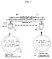
- a transmit clock is sent along with the data signal down a bus until it reaches the receiving device where it can be used to clock the data. This is done so that the delay the signal sees when traveling down the bus wire is matched by the delay of the clock traveling down a matched bus wire. If the same technique is used to send clock and data in both directions, then the transmit and receive data (and clocks) can have phase relationships that depend on the position of the device along the bus.
- 5,432,823 to Gasbarro uses a fixed latency protocol to provide output data at a consistent latency despite clock skews. Because of limitations in circuit performance, the maximum skew, and thus bus length in one embodiment of Gasbarro (see Fig. 2) has a tTR limit. If a device was placed beyond this limit, its output data latency could be uncertain, as the internal synchronization circuits would be near their failure point. Prior art, using a fixed-latency protocol does not provide control for the transition from one latency to another. To eliminate this occurrence, limitations are sometimes placed on the tTR range of operation, and thus potentially on the maximum bus length and device count.
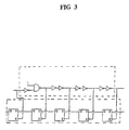
- Portmann et. al. Another system is described in copending application of Portmann et. al., filed July 21, 1997, and commonly assigned with this application (see Fig. 3).
- the corresponding US patent has been published as US 6,205,191.
- Portman describes chains of flip-flops which can gradually be use to re-time data from one domain to another.
- Such re-timing systems are actually a subset of the arbitrary-phase problem; the skew between clocks in Portmann can be easily recreated by adding a matching delay chain on-chip.
- Such systems also suffer from large latency from input to output data, as each flip-flop in the chain can add another cycle of output latency. They also suffer from the same uncertainty at the latency domain switching-point as Gasbarro, and so are unsuitable for use in systems with arbitrary phase-relationships between clocks, such as would be encountered in long-buses.
- the present invention allows for unlimited tTR. By supporting a mixed-latency protocol it allows for tTR greater than 1.0 without uncertainty concerns by creating firm latency domains. Unlike prior art, it maintains the output latency chosen during initialization despite any Vdd or temperature variations that may later occur. In addition, this invention includes circuits that allow operation at higher frequencies than prior art.
- WO 9318463 discloses a circuit taking data synchronized to a receiving clock signal and resynchronizing it to a transmitting clock signal.
- the circuit forms two versions of the received data in the receive clock domain, one delayed by 180 degrees from the other.
- One of these two versions is then selected in accordance with a select signal provided by a circuit measuring the phase difference between the two clocks.
- the selected version is then latched into the transmit clock domain.
- the present invention provides a synchronization circuit having two latching circuits which latch data from a receive clock domain on both the rising and falling edges of a transmit clock.
- the selection of which latch data to use is based on a phase measurement of the phase difference between the receive and transmit clocks, which provides a select signal to a multiplexer connected to the two latching circuits.
- the phase difference is chosen to provide data which is as close as possible to the middle of an overlap region of valid data for the two latches. Once this value has been chosen, it is frozen in a latch after initialization. Since the data could have one, two or more clock cycle latencies from its origin, freezing the clock selection also freezes the latency period for operation of the circuit.
- the synchronization circuit only knows the relative phase difference, not the latency, it can establish a stable operating configuration.
- the terms “receive” and “transmit” clock domains refer to reception and transmission by the synchronization circuit, and does not necessarily correspond to received and transmitted data by a device, such as a memory device.
- the invention is particularly useful in a synchronous memory system in which multiple DRAM are placed along a synchronous bus, at varying latencies from a clock origination point.
- the re-clocked data at each individual DRAM could be in a first latency period or a second latency period.
- the overall system may be equalized by adding latency to devices having less of a latency period to thus provide that all the data will be placed on the bus at the same time.
- the receive clock domain data is provided through a flip-flop clocked by a receive clock.
- the two latching circuits are preferably flip-flops utilizing a precharged sense amp in order to minimize shifting of the clock due to set-up, hold and clock-to-data-out variations.
- the phase measurement circuit has a phase comparator coupled to receive the receive clock and also a clock which is in quadrature with the transmit clock, rather than the transmit clock itself, in order to place the ultimate skip signal at the point of maximum overlap of valid data.
- the output of the phase comparator is provided to an integrator in order to remove any jitter and narrow any uncertainty in the decision point.
- an external transmit clock is used, rather than one that has been synchronized using a DLL or PLL, in order to eliminate another possible source of jitter.
- This invention makes it possible to take input data of arbitrary phase and re-time it into a second mesochronous clock domain with minimal latency.
- a block diagram of the preferred embodiment is shown in Fig. 6. It achieves this re-timing via the Synchronizer 400 and the Skip Circuit 401.
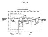
- the synchronizer 400 of Fig. 10 consists of clock-domain crossing circuitry 402 as well as a re-timing latch 308 and multiplexer 310.
- the clock-domain crossing circuitry is where the data is adjusted from the RClk domain into the TClk domain.
- the basic idea behind the clock domain crossing circuitry is straightforward.
- the input data is guaranteed to be at least one clock-cycle in length. Given input data of this type, if it is fed into both rising and falling-edge triggered flip-flops, at any phase offset one of the flip-flops will be able to correctly sample the input data. This concept is illustrated in Fig. 7.
- edge-triggered flip-flop circuits have required times of input stability called setup & hold times, 226 and 228.
- FET-FF 307 The output of FET-FF 307 is then re-timed through latch 308 (see Fig. 10) so that both inputs 216 and 215 to multiplexer 310 have the same timing relationship.
- the outputs are set to be rising-edge based; in an alternate embodiment, a negative-enable latch could be placed after RET-FF 309 instead and the output from the mux would be falling-edge based.
- the two data paths that create the inputs to mux 310 are named ladders, as the re-timing function they perform is akin to a "fish-ladder" used to aid fish in swimming-upstream.
- RET-FF 309 makes up Ladder1 while FET-FF 307 and latch 308 make up Ladder0.
- the function of the Skip circuit 401 is to generate an output signal which represents the phase skew between two input clocks. It must do this with both precision and accuracy in its determination.
- a block diagram of the Skip Circuit is shown as Fig. 25. It generates its output via a phase-comparator 405 followed by an integrator 404 and then a latch 403.
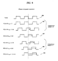
- the phase-comparator compares the input phases by sampling one clock with the other (TxClk is sampled with RClk in one embodiment). If the clocks skew is 0 ⁇ tTR ⁇ 0.5 (see Fig. 8) then the phase-comparator generates an output of 0. If the skew is 0.5 ⁇ tTR ⁇ 1.0 then the phase-comparator generates an output of 1.
- the phase-comparator there is no difference between tTR of 0 and tTR of 1, or between tTR of 0.25 and 1.25, i.e. its behavior is cyclic with phase offset.
- the outputs of the comparator are fed into integrator 404.
- the integrator can be of any conventional form, but contains an input LatchSkip 219 which shuts off integration and ensures full-rail resolution if the integrated value is analog.
- the integrator serves two purposes. First, it takes the mean of any gaussian jitter (noise) distribution on the input clocks.
- the synchronization problem becomes one of proper selection between the Ladder0 and Ladder1 via mux 310.
- This control of mux 310 is accomplished with the Skip Circuit 401.
- tTR is the phase relationship between TxClk and RClk.
- bused systems such as those in Fig. 1, where clocks travel in the same direction as data, it is often required that the clock traveling with the data have its edge located in the center of the valid data window. This can be accomplished through a variety of techniques usually involving a DLL or PLL.
- Fig. 9 the working range of the ladders is represented with tTR as the X-axis.
- tTR the normalized delay difference between TxClk and RClk.
- the working range 232 of Ladder0 is close to one cycle time, in fact it is equal to TCYCLE - (setup + hold time of the flip-flop 307).
- the placement of range 232 begins at (-0.25 + hold) and ends at (0.75 - setup). The reason that the starting and ending are at -0.25 and 0.75, and not O and 1 is that TClk is used for the ladders.
- TClk is in quadrature with TxClk which is used to specify tTR.
- output from Ladder0 in range 233 will have one additional cycle of latency relative to its operation in range 232, and is said to be in latency domain 2 (see also Fig. 4). Both ladders, and indeed any synchronization circuitry will exhibit this behavior if the clock skews are pushed beyond their limit.
- the control of these different latency domains is a key innovation in this invention.
- Ladder0 operates with latency of 1 and 2 in ranges 232 and 233, so does Ladder1 within ranges 231 and 234.
- skip 230 is used to seamlessly choose between Ladder0 and Ladder1 at tTR of 0.5.
- Skip is also used to transition from Ladder1 back to Ladder0 at tTR of 1.0. While the Skip transition at tTR of 0.5 was in no way visible at the output (i.e., the signals 236, 237, and 238 of Fig. 4 are identical), the outputs 236-238 are quite different from output 239.
- the resynchronization circuitry may be used in a system consisting of bused devices as in Fig. 1, it is critical that the devices not change the latency of their output data if they happen to be placed at exactly a latency boundary.
- the skip latch 403 (Fig. 25) is used to ensure that after a period of initialization, the value of skip is latched and can no longer change. This guarantees that the output latency will not change unless the circuit is reset by re-assertion of LatchSkip 219. After de-assertion of LatchSkip the output data latency can be guaranteed to not change. Fail-safe operation requires no synchronization failure in the synchronizer 400 as well as stable output latency.
- the use of the synchronizer and skip circuit in a system requires a control signal to freeze the output of the Skip Circuit 401, called LatchSkip 219 (see Fig. 25). The assertion of this signal causes the skip value to be sampled and held inside latch 403 of the Skip Circuit 401. If the synchronizer is to be used in systems which span more than one clock cycle this function is normally accomplished during initialization, before the output of the synchronization circuit can be used. This avoids the possibility of outputs with different latencies.
- LatchSkip 219 There are multiple possible ways of generating LatchSkip 219 to achieve this function. It can simply be asserted through a device reset. In this way when reset is de-asserted the skip output will be latched and the output latency will be fixed unless the device is reset. There are several other ways LatchSkip 219 can be generated. There are frequently initialization packets that are required to setup a device before use. In this case LatchSkip can be generated by a strobe used to receive one of these setup packets. By ensuring that a setup packet asserts LatchSkip 219, the skip output can be guaranteed to be stable before the synchronization circuit is actually used to re-time output data. Alternately, register or mode bits inside a device can also control the strobing of LatchSkip 219. Combining register control with other techniques allows for the flexibility of later skip evaluation and latching without requiring a device reset.
- the system may be able to run at multiple different operating frequencies. This might be done in order to accommodate different power modes, where lower power can be obtained at lower frequencies by disabling some high-power circuitry.
- multiple skip latches and multiple LatchSkip signals can be used as shown in Fig. 26.
- initialization would include the evaluation of the phase comparator and integrator at each operating frequency followed by latching into separate skip latches. The appropriate value of skip for the current operating frequency can then be selected by simply using the corresponding latch output.
- the Timing Synchronizer passes data between sequential circuits of two arbitrary-phased mesochronous clock domains.
- the synchronizer ensures signals are re-timed fail-safe or without metastability and timing glitches, and with minimum latency from circuits of one clock domain to circuits of another clock domain.
- the synchronizer when used to time output data transmission on a bus system such as one shown in Fig. 1, the synchronizer times the output data so it arrives within a particular cycle at the destination.
- Timing synchronizer A preferred embodiment of the timing synchronizer is shown in Fig. 10.
- This circuit consists of Rclk flip-flop 306, Tclk flip-flops 307, 309, Tclk latch 308, and Multiplexer 310.
- the synchronizer may be partitioned into two signal paths or ladders (Ladder0, Ladder1), each with its own latency characteristics. Data propagates through Ladder0 via nodes 217, 603, 214, 216; Data propagates through Ladder1 via nodes 217, 603, 215.
- flip-flop 306 samples input Data In 217 every RClk cycle, and holds output 603 valid for one clock cycle (see Fig. 11).
- the value at node 603 may transition depending on DataIn 217.
- data cannot be reliably sampled by edge triggered flip-flops.
- TClk flip-flop 307 and 309 sample data on the falling and rising edges of TClk respectively, at least one of these two flip-flops is guaranteed to sample data from node 603 when it is not changing. This is required for fail-safe data resynchronization.
- output from Ladder0 at node 216 may be zero or one cycle later than the output from Ladder1 at node 215.
- Each ladder operates over a particular tTR range of operation without encountering problems with metastability.
- each ladder's operating range occurs when the center 613 of the Valid Data window 603 aligns with the ladder's sampling TClk edge.
- the center of the overlap between the two ladders occurs when Valid Data Center 613 is equidistant from the two sampling TClk edges as in Fig. 12.
- Region (a) of Fig. 14 shows the operating ranges of the two ladders in the Synchronizer circuits versus tTR phase values.
- a particular tTR value may be interpreted as an indicator of the position on the bus.
- Ladder0 ideally operates for tTR range of -0.25 to 0.75 (see Fig. 14(a)/622).
- Ladder1 ideally operates for tTR range of 0.25 to 1.25 (see Fig. 14(a)/622).
- the overlap window between ladders 621 and 622 in indicates the region where both Ladder1 and Ladder0 outputs are the same.
- Ladder0 623 is similar to Ladder0 621. However, its output is shifted 1 Cycle later in time.
- the ends of each ladder shown in region (a) of Fig. 14 indicate tTR operation ranges beyond which the particular ladder is unreliable.
- Fig. 17 and Fig. 18 show the waveforms of flip-flops 306 and 307 (shown in Fig. 10) for a typical and slow performance conditions respectively.
- the varying circuit performance is due to varying integrated circuit transistor processes, power supply voltage and operating temperature of practical systems.
- Ladder position shifts are caused by clock-to-data-out delay variation of flip-flop 306 and setup/hold variations of flip-flop 307. These variations are equivalent to shifting Rclk and Tclk (thus effective tTR) in the ideal case shown in Fig. 16. Any mismatched clock buffering of Tclk and Rclk within the integrated circuit contributes additional ladder shifts.
- the circuit implementation of the synchronizer addresses the aforementioned Ladder shifts and shrinkage for maximum timing margin over varying process, voltage, and temperature conditions.
- a partial circuit schematic of one implementation is shown in Fig. 19. This circuit addresses the sources of Ladder shifts and shrinkage with delay compensation and faster circuit performance.
- a precharged sense amp is used for the second stage flip-flops.
- the clocked sense-amp latching delay varies approximately with the clock-to-data-out delay of the previous stage latch. So in slower transistor performance conditions, the clocked sense-amp will delay its sampling point to compensate for the added clock-to-data-out delay at nodes 806 and Ladder17.
- the use of differential signals 806, 807 instead of single-ended signal 603 increases the sense-amp gain, and lowers the setup and hold of flip-flops 307, 309.
- the Synchronizer circuit shown in Fig. 10 uses the falling edge of RClk 831/830 and the rising and falling edges of TClk 808/809 to generate overlapping Ladder0 and Ladder1. This configuration generates rising-edge triggered outputs.
- the synchronizer can use the rising and falling edges of RClk with one sampling edge of Tclk, an embodiment of which is shown in Fig. 20.
- the basic premise used to achieve clock domain crossing is to use circuits clocked with different phases of one clock domain to pass data into another domain. The end results are overlapping ladders similar to those shown in Fig. 14.
- FIG. 21 Another embodiment of the timing synchronizer is shown in Fig. 21, and consists of four overlapping ladders 961/971, 962/972, 963/973 and 964/974.
- the resultant ladder ranges are shown versus tTR value in Fig. 22.
- the ideal overlap between each ladder is 3/4 TCYCLE. This allows substantially more margin for errors in ladder shifts, narrowing, and placements of Mux 979 select controls.
- Toverlap Tcycle num ( ladders )-1 num ( ladders )
- the above equation shows diminishing increase of overlap margin with an increased number of ladders. Also, an increasing number of ladders requires a larger number of mux select controls.
- FIG. 23 A different embodiment of the synchronizer is shown in Fig. 23.
- This synchronizer realigns the data with the use of a "blended" clock IntClk 1005.
- the blended clock has a phase which is halfway between RClk and TClk as shown in Fig. 24.
- the synchronizer includes three sequentially coupled latches 1003, 1006, 1009 that are clocked by RClk 1002, IntClk 1005 and TClk 1008, respectively.
- Node 1004 represents RClk valid data, which moves later in phase relative to TClk as tTR increases.
- This synchronizer circuit preserves the output delay of Data Out/1010 relative to TClk over the entire tTR range of 0 to 1.
- the input clocks Rclk and TClk are aligned, and the synchronizer has a three clock cycle delay through the circuit.
- the Latency of the synchronizer circuit decreases to compensate for the increased delay of RClk relative to TClk. Therefore, Data Out 1010 is captured by the same TClk edge even as the RClk valid data 1004 is delayed by up to one clock cycle.
- the inputs required for this synchronizer are RClk 1002, IntClk 1005, TClk 1008, and RClk-domain Data In 1001.
- An external multiplexer select generator is not required.
- IntClk 1005 is generated by a phase interpolator or mixer circuit 1007.
- the Skip Circuit 401 (see Fig. 25) is made up of a phase comparator 405, an integrator 404, and a latch 403.
- the purpose of the Skip Circuit is to generate a very accurate measurement of tTR with minimal-width uncertainty regions. It also provides the capability to latch the output value after initialization, eliminating the possibility of multiple operating latencies if tTR is near a latency-domain boundary.
- a preferred embodiment of the phase-comparator in Fig. 27 is used in order to provide an accurate measurement with minimum uncertainty. It contains high-gain narrow-uncertainty-window data receivers of the same type that are used to sample bus data. In the preferred embodiment these are used in conjunction with a DLL or PLL which has aligned RClk so any receiver setup+hold time has been removed.
- Using a data receiver to sample the external signal TxClk has two advantages over sampling an internal clock. First, it gives the most accurate measurement of bus position as internal clocks can be skewed by clock recovery circuits for a number of reasons. Second, it provides the lowest-jitter source of transmit-domain phase information available. Any clock recovered with a DLL or PLL (e.g. TClk) will necessarily have higher jitter than at the input clock.
- a simple FET (falling-edge-triggered) data receiver could be used to generate the phase-comparator output.
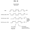
- a single-data receiver used in this fashion could incorrectly determine the value of tTR if it was sampling a duty-cycle distorted clock while being clocked by a duty-cycle corrected clock (see Fig. 28).
- the phase comparator can tolerate a non-50% duty-cycle on TxClk. This can be more easily understood by observing the different characteristics of waveforms 248, 249 and 251 at the time of both the RClk rising edge 253 and the RClk falling edge 252.
- phase-comparator 405 uses a Quadrature Phase Detector to compare RClk and TClk, the Quadrature Phase Detector having output which indicates when the clocks are in quadrature. This eliminates the need for the use of a clock which is in quadrature to TClk, and allows for the combined system to only use two clocks.
- the Skip Circuit integrator 404 consists of a standard integrator, which serves to narrow the uncertainty window created by a jitter distribution (such as a gaussian distribution). Any clock will have a certain amount of random noise which shows up as a distribution of phase. Using an integrator on the output of the phase-comparator ensures that signal 243's transition will be closest to the mean-point of the jitter distributions of both TxClk 220 and RClk 211, while at any single-point in time the raw phase-comparator output 242 could be the result of comparison to an extreme of the clock jitter distributions.
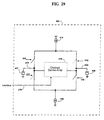
- An integrator 404 preferred embodiment shown in Fig. 29 is an analog integrator with steered up and down current sources 416 and 435 into capacitors 417 and 436 which create a differential voltage on output nodes 243 and 270.
- the steering of these currents is controlled by switches driven by the comparator output 242.
- the integrator is allowed to run for at least 40 cycles after the clocks settle, in order to ensure an adequate gaussian distribution of the clock inputs.
- the LatchSkip 219 signal is asserted and de-asserted to both the integrator and the skip latch 403 turning off integration. If the integrator is analog, this signal also asserts a high-gain sense-amp 415. LatchSkip 219 also closes the skip latch 403 so the Skip Circuit output will not change unless LatchSkip 219 is re-asserted.
- the Synchronizer 400 and Skip Circuit 401 make up a synchronization system. Both elements are required in the preferred embodiment in order to properly synchronize data between two mesochronous clock domains. This invention allows for 1) high operating frequency and then 2) low latency while maintaining fail-safe operation.
- the Synchronizer In order to achieve fail-safe operation, the Synchronizer must not fail to both properly pass and re-time the incoming data.
- the most significant failure mechanism is if the improper ladder for the current operating conditions (tTR, Voltage, temperature) is used. This can come about due to error sources which this invention minimizes.
- error sources which this invention minimizes.
- the multiple possible error sources result in an equation which limits the cycle-time of the system. Possible sources of error include:
- RClk or TxClk/TClk may be shifted earlier or later by a constant time or phase delay so the first latency domain boundary occurs at a tTR other than 1.
- both the Synchronizer 400 and the Skip Circuit 401 use RClk as the starting reference both circuits will shift together. All latency domains remain 1 cycle wide, and so all boundary ends will move as well.
- the combination of the Synchronizer and Skip circuit provide high frequency fail-safe synchronization for mesochronous systems such as that of Fig. 1.
- Arbitrary phase delays are possible while fail-safe latency is minimized and output latency is kept constant despite changes in the circuit's operating point.
- Fig. 26 To accommodate switching between multiple operating frequencies without requiring re-evaluation of skip an alternate embodiment of the Skip circuit 430 can be used as shown in Fig. 26.
- the single Skip Latch 403 of Fig. 25 has been replaced by multiple skip latches 431-433.
- the single LatchSkip signal 219 of Fig. 25 has been replaced by LatchSkip_F1 to LatchSkip_Fn 260-265. There is one latch and one LatchSkip signal for each desired operating frequency.
- each of the desired operating frequencies is selected and initialized.
- the appropriate LatchSkip_Fx signal is asserted using one of the techniques described previously.
- the correct value for Skip at each desired frequency is stored in the respective skip latches 431-433.
- the device can then simply select the appropriate Skip value depending on its current operating frequency without having to wait for the Skip Circuit to reevaluate.
- a multiplexing circuit can connect a selected skip latch to skip input 213 of Fig. 10.
Landscapes
- Engineering & Computer Science (AREA)
- Theoretical Computer Science (AREA)
- Signal Processing (AREA)
- Computer Networks & Wireless Communication (AREA)
- General Physics & Mathematics (AREA)
- Physics & Mathematics (AREA)
- General Engineering & Computer Science (AREA)
- Dram (AREA)
- Hardware Redundancy (AREA)
- Information Transfer Systems (AREA)
- Retry When Errors Occur (AREA)
- Exchange Systems With Centralized Control (AREA)
- Stabilization Of Oscillater, Synchronisation, Frequency Synthesizers (AREA)
- Synchronisation In Digital Transmission Systems (AREA)
Applications Claiming Priority (3)
| Application Number | Priority Date | Filing Date | Title |
|---|---|---|---|
| US6150597P | 1997-10-10 | 1997-10-10 | |
| US61505P | 1997-10-10 | ||
| PCT/US1998/021448 WO1999019806A1 (en) | 1997-10-10 | 1998-10-09 | Method and apparatus for fail-safe resynchronization with minimum latency |
Publications (2)
| Publication Number | Publication Date |
|---|---|
| EP1031093A1 EP1031093A1 (en) | 2000-08-30 |
| EP1031093B1 true EP1031093B1 (en) | 2003-02-05 |
Family
ID=22036219
Family Applications (1)
| Application Number | Title | Priority Date | Filing Date |
|---|---|---|---|
| EP98952237A Expired - Lifetime EP1031093B1 (en) | 1997-10-10 | 1998-10-09 | Method and apparatus for fail-safe resynchronization with minimum latency |
Country Status (8)
| Country | Link |
|---|---|
| US (3) | US6473439B1 (https=) |
| EP (1) | EP1031093B1 (https=) |
| JP (1) | JP4484359B2 (https=) |
| KR (1) | KR100603687B1 (https=) |
| AT (1) | ATE232317T1 (https=) |
| AU (1) | AU9798698A (https=) |
| DE (1) | DE69811262T2 (https=) |
| WO (1) | WO1999019806A1 (https=) |
Cited By (1)
| Publication number | Priority date | Publication date | Assignee | Title |
|---|---|---|---|---|
| US12092688B2 (en) | 2020-04-09 | 2024-09-17 | Advantest Corporation | Circuit for transferring data from one clock domain to another |
Families Citing this family (95)
| Publication number | Priority date | Publication date | Assignee | Title |
|---|---|---|---|---|
| AU9798698A (en) | 1997-10-10 | 1999-05-03 | Rambus Incorporated | Method and apparatus for fail-safe resynchronization with minimum latency |
| US6799280B1 (en) * | 2000-01-04 | 2004-09-28 | Advanced Micro Devices, Inc. | System and method for synchronizing data transfer from one domain to another by selecting output data from either a first or second storage device |
| US20020097682A1 (en) * | 2000-06-02 | 2002-07-25 | Enam Syed K. | Low frequency loop-back in a high speed optical transceiver |
| FR2810009B1 (fr) * | 2000-06-09 | 2002-09-27 | Otico | Dispositif d'entrainement a chenille pour vehicule tout terrain |
| JP3857230B2 (ja) * | 2000-10-11 | 2006-12-13 | Nttエレクトロニクス株式会社 | 位相比較回路 |
| DE10059758A1 (de) * | 2000-11-30 | 2002-06-20 | Bosch Gmbh Robert | Verfahren zum Empfangen von Daten |
| US20020194518A1 (en) * | 2001-06-06 | 2002-12-19 | Chang Kun-Yung Ken | Apparatus and method for generating a skip signal |
| US7194056B2 (en) | 2001-06-25 | 2007-03-20 | Rambus Inc. | Determining phase relationships using digital phase values |
| US6920540B2 (en) | 2001-10-22 | 2005-07-19 | Rambus Inc. | Timing calibration apparatus and method for a memory device signaling system |
| TWI235917B (en) | 2002-04-15 | 2005-07-11 | Via Tech Inc | High speed data transmitter and transmission method thereof |
| CN100421096C (zh) * | 2002-05-08 | 2008-09-24 | 威盛电子股份有限公司 | 高速数据传输器及其传输方法 |
| US7149874B2 (en) * | 2002-08-16 | 2006-12-12 | Micron Technology, Inc. | Memory hub bypass circuit and method |
| US7359407B1 (en) * | 2002-08-27 | 2008-04-15 | Cypress Semiconductor Corp. | Data interface that is configurable into separate modes of operation for sub-bit de-skewing of parallel-fed data signals |
| JP3704709B2 (ja) | 2002-10-02 | 2005-10-12 | 日本電気株式会社 | データ再同期化装置 |
| US6729994B1 (en) * | 2002-10-29 | 2004-05-04 | General Motors Corporation | Multi-speed transmission mechanisms with three planetary gearsets and clutch input |
| US7231009B2 (en) * | 2003-02-19 | 2007-06-12 | Silicon Image, Inc. | Data synchronization across an asynchronous boundary using, for example, multi-phase clocks |
| US6864722B2 (en) * | 2003-05-09 | 2005-03-08 | Hewlett-Packard Development Company, L.P. | Phase detector for a programmable clock synchronizer |
| US7275171B2 (en) | 2003-05-22 | 2007-09-25 | Rambus Inc. | Method and apparatus for programmable sampling clock edge selection |
| US7133991B2 (en) * | 2003-08-20 | 2006-11-07 | Micron Technology, Inc. | Method and system for capturing and bypassing memory transactions in a hub-based memory system |
| US7072355B2 (en) * | 2003-08-21 | 2006-07-04 | Rambus, Inc. | Periodic interface calibration for high speed communication |
| US7136958B2 (en) | 2003-08-28 | 2006-11-14 | Micron Technology, Inc. | Multiple processor system and method including multiple memory hub modules |
| US7120743B2 (en) * | 2003-10-20 | 2006-10-10 | Micron Technology, Inc. | Arbitration system and method for memory responses in a hub-based memory system |
| US7073146B2 (en) * | 2003-10-30 | 2006-07-04 | Atrenta Inc. | Method for clock synchronization validation in integrated circuit design |
| KR20050076202A (ko) * | 2004-01-20 | 2005-07-26 | 삼성전자주식회사 | 지연 신호 발생 회로 및 이를 포함한 메모리 시스템 |
| US7095789B2 (en) | 2004-01-28 | 2006-08-22 | Rambus, Inc. | Communication channel calibration for drift conditions |
| US7158536B2 (en) * | 2004-01-28 | 2007-01-02 | Rambus Inc. | Adaptive-allocation of I/O bandwidth using a configurable interconnect topology |
| US7400670B2 (en) | 2004-01-28 | 2008-07-15 | Rambus, Inc. | Periodic calibration for communication channels by drift tracking |
| US8422568B2 (en) | 2004-01-28 | 2013-04-16 | Rambus Inc. | Communication channel calibration for drift conditions |
| US7412574B2 (en) * | 2004-02-05 | 2008-08-12 | Micron Technology, Inc. | System and method for arbitration of memory responses in a hub-based memory system |
| US7788451B2 (en) | 2004-02-05 | 2010-08-31 | Micron Technology, Inc. | Apparatus and method for data bypass for a bi-directional data bus in a hub-based memory sub-system |
| FR2867334B1 (fr) * | 2004-03-05 | 2006-04-28 | Thales Sa | Procede et dispositif d'echantillonnage de donnees numeriques dans une transmission synchrone, avec maintien de l'integrite binaire |
| US6961862B2 (en) | 2004-03-17 | 2005-11-01 | Rambus, Inc. | Drift tracking feedback for communication channels |
| US7257683B2 (en) | 2004-03-24 | 2007-08-14 | Micron Technology, Inc. | Memory arbitration system and method having an arbitration packet protocol |
| US7447240B2 (en) | 2004-03-29 | 2008-11-04 | Micron Technology, Inc. | Method and system for synchronizing communications links in a hub-based memory system |
| US7159199B2 (en) * | 2004-04-02 | 2007-01-02 | Stmicroelectronics Limited | Method for verifying adequate synchronization of signals that cross clock environments and system |
| US6980042B2 (en) * | 2004-04-05 | 2005-12-27 | Micron Technology, Inc. | Delay line synchronizer apparatus and method |
| US7535985B2 (en) | 2004-04-26 | 2009-05-19 | Panasonic Corporation | Resynchronization circuit |
| US20050259692A1 (en) * | 2004-05-19 | 2005-11-24 | Zerbe Jared L | Crosstalk minimization in serial link systems |
| US7363419B2 (en) | 2004-05-28 | 2008-04-22 | Micron Technology, Inc. | Method and system for terminating write commands in a hub-based memory system |
| US7978754B2 (en) * | 2004-05-28 | 2011-07-12 | Rambus Inc. | Communication channel calibration with nonvolatile parameter store for recovery |
| US7516029B2 (en) | 2004-06-09 | 2009-04-07 | Rambus, Inc. | Communication channel calibration using feedback |
| US7535958B2 (en) * | 2004-06-14 | 2009-05-19 | Rambus, Inc. | Hybrid wired and wireless chip-to-chip communications |
| US7489739B2 (en) * | 2004-09-17 | 2009-02-10 | Rambus, Inc. | Method and apparatus for data recovery |
| US20060098770A1 (en) * | 2004-11-09 | 2006-05-11 | Harper William F | Synchronizer for passing data from a first system to a second system |
| US7199728B2 (en) * | 2005-01-21 | 2007-04-03 | Rambus, Inc. | Communication system with low power, DC-balanced serial link |
| US7088270B1 (en) * | 2005-01-21 | 2006-08-08 | Rambus, Inc. | Low power, DC-balanced serial link |
| US7061406B1 (en) * | 2005-01-21 | 2006-06-13 | Rambus, Inc. | Low power, DC-balanced serial link transmitter |
| CN103116565A (zh) | 2005-04-21 | 2013-05-22 | 提琴存储器公司 | 可配置的开关原件、互连网络及布局网络间相互连接方法 |
| US9582449B2 (en) | 2005-04-21 | 2017-02-28 | Violin Memory, Inc. | Interconnection system |
| US9384818B2 (en) | 2005-04-21 | 2016-07-05 | Violin Memory | Memory power management |
| US8112655B2 (en) * | 2005-04-21 | 2012-02-07 | Violin Memory, Inc. | Mesosynchronous data bus apparatus and method of data transmission |
| US7332950B2 (en) * | 2005-06-14 | 2008-02-19 | Micron Technology, Inc. | DLL measure initialization circuit for high frequency operation |
| US9420332B2 (en) * | 2006-07-06 | 2016-08-16 | Qualcomm Incorporated | Clock compensation techniques for audio decoding |
| US7653167B2 (en) * | 2006-09-07 | 2010-01-26 | Intel Corporation | Phase deglitch circuit for phase interpolator for high-speed serial I/O applications |
| EP1901474B1 (en) * | 2006-09-13 | 2011-11-30 | Stmicroelectronics Sa | System for synchronizing modules in an integrated circuit in mesochronous clock domains |
| US20080109672A1 (en) * | 2006-11-08 | 2008-05-08 | Sicortex, Inc | Large scale computing system with multi-lane mesochronous data transfers among computer nodes |
| EP1936857A1 (en) * | 2006-12-22 | 2008-06-25 | Stmicroelectronics Sa | System for transmitting data between transmitter and receiver modules on a channel provided with a flow control link |
| US7836324B2 (en) * | 2007-02-09 | 2010-11-16 | Apple Inc. | Oversampling-based scheme for synchronous interface communication |
| US7908574B2 (en) * | 2007-05-09 | 2011-03-15 | Synopsys, Inc. | Techniques for use with automated circuit design and simulations |
| US8756557B2 (en) * | 2007-05-09 | 2014-06-17 | Synopsys, Inc. | Techniques for use with automated circuit design and simulations |
| US7904859B2 (en) * | 2007-05-09 | 2011-03-08 | Synopsys, Inc. | Method and apparatus for determining a phase relationship between asynchronous clock signals |
| US7984400B2 (en) * | 2007-05-09 | 2011-07-19 | Synopsys, Inc. | Techniques for use with automated circuit design and simulations |
| US7619449B2 (en) * | 2007-06-07 | 2009-11-17 | Micron Technology, Inc. | Method and apparatus for synchronous clock distribution to a plurality of destinations |
| KR100929824B1 (ko) * | 2008-05-06 | 2009-12-07 | 주식회사 하이닉스반도체 | 반도체 소자 |
| JP5276928B2 (ja) * | 2008-08-29 | 2013-08-28 | 株式会社日立製作所 | 信号再生回路向け位相比較回路及び信号再生回路向け位相比較回路を備える光通信装置 |
| US8161313B2 (en) * | 2008-09-30 | 2012-04-17 | Mosaid Technologies Incorporated | Serial-connected memory system with duty cycle correction |
| US8181056B2 (en) * | 2008-09-30 | 2012-05-15 | Mosaid Technologies Incorporated | Serial-connected memory system with output delay adjustment |
| CN102458385A (zh) * | 2009-05-08 | 2012-05-16 | 3M创新有限公司 | 口腔护理方法和套件 |
| US9565036B2 (en) * | 2009-06-30 | 2017-02-07 | Rambus Inc. | Techniques for adjusting clock signals to compensate for noise |
| US9465756B2 (en) * | 2009-12-23 | 2016-10-11 | Violin Memory Inc. | Configurable interconnection system |
| US8261121B2 (en) * | 2009-12-24 | 2012-09-04 | Nvidia Corporation | Command latency reduction and command bandwidth maintenance in a memory circuit |
| US8707080B1 (en) * | 2011-07-12 | 2014-04-22 | Emc Corporation | Simple circular asynchronous clock domain crossing technique for digital data |
| US8415981B2 (en) * | 2011-08-15 | 2013-04-09 | Mediatek Singapore Pte. Ltd. | Integrated circuit device, synchronisation module, electronic device and method therefor |
| US8782458B2 (en) * | 2011-11-29 | 2014-07-15 | Advanced Micro Devices, Inc. | System and method of data communications between electronic devices |
| CN103247325B (zh) * | 2012-02-07 | 2017-03-01 | 北京兆易创新科技股份有限公司 | 一种串行i/o接口快闪存储器 |
| CN103247323B (zh) * | 2012-02-07 | 2016-05-04 | 北京兆易创新科技股份有限公司 | 一种串行接口快闪存储器 |
| US8836394B2 (en) * | 2012-03-26 | 2014-09-16 | Rambus Inc. | Method and apparatus for source-synchronous signaling |
| TWI449338B (zh) * | 2012-04-18 | 2014-08-11 | Univ Nat Sun Yat Sen | 具數位校正之峰值偵測器 |
| KR101950320B1 (ko) * | 2012-06-29 | 2019-02-20 | 에스케이하이닉스 주식회사 | 위상 검출 회로 및 이를 이용한 동기 회로 |
| US8760204B2 (en) * | 2012-11-20 | 2014-06-24 | Nvidia Corporation | Variation-tolerant periodic synchronizer |
| WO2014174960A1 (ja) | 2013-04-22 | 2014-10-30 | シャープ株式会社 | スタイラスペン、タッチパネルシステム、および電子機器 |
| US9213487B2 (en) | 2013-10-16 | 2015-12-15 | Qualcomm Incorporated | Receiver architecture for memory reads |
| KR102248279B1 (ko) * | 2014-06-13 | 2021-05-07 | 삼성전자주식회사 | 불휘발성 메모리 및 메모리 컨트롤러를 포함하는 스토리지 장치, 그리고 불휘발성 메모리 및 메모리 컨트롤러 사이의 통신을 중개하는 리타이밍 회로의 동작 방법 |
| US10481203B2 (en) * | 2015-04-04 | 2019-11-19 | Nvidia Corporation | Granular dynamic test systems and methods |
| US9541990B2 (en) | 2015-04-21 | 2017-01-10 | Cypress Semiconductor Corporation | Asynchronous transceiver for on-vehicle electronic device |
| US10444280B2 (en) | 2015-10-27 | 2019-10-15 | Nvidia Corporation | Independent test partition clock coordination across multiple test partitions |
| US10095263B1 (en) * | 2015-12-15 | 2018-10-09 | Marvell International Ltd. | Apparatus and method for calibrating signal synchronization |
| US10623174B1 (en) | 2018-12-12 | 2020-04-14 | Xilinx, Inc. | Low latency data transfer technique for mesochronous divided clocks |
| US11622005B2 (en) * | 2019-03-27 | 2023-04-04 | Boe Technology Group Co., Ltd. | Internet of Things system, central control device, application device and communication methods |
| CN111797043B (zh) * | 2019-04-08 | 2022-04-26 | 达发科技(苏州)有限公司 | 跨时脉域系统 |
| US10924091B2 (en) * | 2019-07-02 | 2021-02-16 | Stmicroelectronics International N.V. | Immediate fail detect clock domain crossing synchronizer |
| US10965441B1 (en) * | 2019-10-10 | 2021-03-30 | Rohde & Schwarz Gmbh & Co. Kg | Frame trigger recreation method and frame trigger recreator |
| GB202014083D0 (en) | 2020-09-08 | 2020-10-21 | Nordic Semiconductor Asa | Clock domain crossing |
| US11829640B2 (en) | 2020-10-27 | 2023-11-28 | Rambus Inc. | Asynchronous arbitration across clock domains for register writes in an integrated circuit chip |
| US11677391B1 (en) * | 2021-01-28 | 2023-06-13 | Rambus Inc. | Low-power multi-domain synchronizer |
Family Cites Families (26)
| Publication number | Priority date | Publication date | Assignee | Title |
|---|---|---|---|---|
| US4819081A (en) * | 1987-09-03 | 1989-04-04 | Intel Corporation | Phase comparator for extending capture range |
| US5551050A (en) | 1989-12-20 | 1996-08-27 | Texas Instruments Incorporated | System and method using synchronized processors to perform real time internal monitoring of a data processing device |
| JPH04262618A (ja) * | 1991-02-18 | 1992-09-18 | Advantest Corp | 位相検波器 |
| DE4345604B3 (de) * | 1992-03-06 | 2012-07-12 | Rambus Inc. | Vorrichtung zur Kommunikation mit einem DRAM |
| JPH06132972A (ja) * | 1992-10-20 | 1994-05-13 | Fujitsu Ltd | 広帯域isdn遠隔多重装置 |
| US5757868A (en) * | 1994-02-16 | 1998-05-26 | Motorola, Inc. | Digital phase detector with integrated phase detection |
| US5509038A (en) * | 1994-04-06 | 1996-04-16 | Hal Computer Systems, Inc. | Multi-path data synchronizer system and method |
| US5550875A (en) | 1994-12-29 | 1996-08-27 | Unisys Corporation | Apparatus and method for residual error clock skew bound, and clocking therewith |
| US5646519A (en) * | 1995-06-07 | 1997-07-08 | Symmetricom, Inc. | Digital phase detector employing a digitally controllable delay line |
| JP3873089B2 (ja) | 1995-06-07 | 2007-01-24 | 三星電子株式会社 | 互いに非同期の2つのバス間でデータ転送を同期する際の累積時間遅延を低減するもの |
| US5652530A (en) | 1995-09-29 | 1997-07-29 | Intel Corporation | Method and apparatus for reducing clock-data skew by clock shifting |
| JP2806863B2 (ja) * | 1996-02-27 | 1998-09-30 | 日本電気エンジニアリング株式会社 | ビット同期回路 |
| US5799048A (en) * | 1996-04-17 | 1998-08-25 | Sun Microsystems, Inc. | Phase detector for clock synchronization and recovery |
| JP3467975B2 (ja) * | 1996-06-27 | 2003-11-17 | 安藤電気株式会社 | 位相検出回路 |
| US6205191B1 (en) | 1997-07-21 | 2001-03-20 | Rambus Inc. | Method and apparatus for synchronizing a control signal |
| US6008680A (en) * | 1997-08-27 | 1999-12-28 | Lsi Logic Corporation | Continuously adjustable delay-locked loop |
| AU9798698A (en) * | 1997-10-10 | 1999-05-03 | Rambus Incorporated | Method and apparatus for fail-safe resynchronization with minimum latency |
| TW388795B (en) * | 1997-12-24 | 2000-05-01 | Via Tech Inc | Auxiliary device and method for signal testing |
| US6150889A (en) * | 1998-08-03 | 2000-11-21 | Motorola, Inc. | Circuit and method for minimizing recovery time |
| US6334163B1 (en) * | 1999-03-05 | 2001-12-25 | International Business Machines Corp. | Elastic interface apparatus and method therefor |
| US6100722A (en) * | 1999-07-28 | 2000-08-08 | Cypress Semiconductor Corp. | Phase detector with extended linear range |
| US6172540B1 (en) * | 1999-08-16 | 2001-01-09 | Intel Corporation | Apparatus for fast logic transfer of data across asynchronous clock domains |
| US6799280B1 (en) * | 2000-01-04 | 2004-09-28 | Advanced Micro Devices, Inc. | System and method for synchronizing data transfer from one domain to another by selecting output data from either a first or second storage device |
| US6987823B1 (en) * | 2000-02-07 | 2006-01-17 | Rambus Inc. | System and method for aligning internal transmit and receive clocks |
| US6798259B2 (en) * | 2001-08-03 | 2004-09-28 | Micron Technology, Inc. | System and method to improve the efficiency of synchronous mirror delays and delay locked loops |
| US6614314B2 (en) * | 2001-12-03 | 2003-09-02 | Gennum Corporation | Non-linear phase detector |
-
1998
- 1998-10-09 AU AU97986/98A patent/AU9798698A/en not_active Abandoned
- 1998-10-09 DE DE69811262T patent/DE69811262T2/de not_active Expired - Fee Related
- 1998-10-09 US US09/169,372 patent/US6473439B1/en not_active Expired - Fee Related
- 1998-10-09 KR KR1020007003852A patent/KR100603687B1/ko not_active Expired - Fee Related
- 1998-10-09 JP JP2000516290A patent/JP4484359B2/ja not_active Expired - Lifetime
- 1998-10-09 AT AT98952237T patent/ATE232317T1/de not_active IP Right Cessation
- 1998-10-09 WO PCT/US1998/021448 patent/WO1999019806A1/en not_active Ceased
- 1998-10-09 EP EP98952237A patent/EP1031093B1/en not_active Expired - Lifetime
-
2002
- 2002-10-28 US US10/282,531 patent/US6949958B2/en not_active Expired - Fee Related
-
2005
- 2005-09-27 US US11/237,276 patent/US7288973B2/en not_active Expired - Fee Related
Cited By (1)
| Publication number | Priority date | Publication date | Assignee | Title |
|---|---|---|---|---|
| US12092688B2 (en) | 2020-04-09 | 2024-09-17 | Advantest Corporation | Circuit for transferring data from one clock domain to another |
Also Published As
| Publication number | Publication date |
|---|---|
| ATE232317T1 (de) | 2003-02-15 |
| DE69811262D1 (de) | 2003-03-13 |
| AU9798698A (en) | 1999-05-03 |
| KR100603687B1 (ko) | 2006-07-20 |
| DE69811262T2 (de) | 2003-11-27 |
| EP1031093A1 (en) | 2000-08-30 |
| WO1999019806A1 (en) | 1999-04-22 |
| US6949958B2 (en) | 2005-09-27 |
| JP4484359B2 (ja) | 2010-06-16 |
| KR20010031036A (ko) | 2001-04-16 |
| JP2001520417A (ja) | 2001-10-30 |
| US20060022724A1 (en) | 2006-02-02 |
| US6473439B1 (en) | 2002-10-29 |
| US20030053489A1 (en) | 2003-03-20 |
| US7288973B2 (en) | 2007-10-30 |
Similar Documents
| Publication | Publication Date | Title |
|---|---|---|
| EP1031093B1 (en) | Method and apparatus for fail-safe resynchronization with minimum latency | |
| US7974375B2 (en) | Linear phase detector and clock/data recovery circuit thereof | |
| US11061432B2 (en) | Data handoff between two clock domains sharing a fundamental beat | |
| JP4065234B2 (ja) | 同期式チップーチップシステムのデータリカバリ装置 | |
| US7765074B2 (en) | Circuit, apparatus and method for capturing a representation of a waveform from a clock-data recovery (CDR) unit | |
| US7978802B1 (en) | Method and apparatus for a mesochronous transmission system | |
| US7170964B2 (en) | Transition insensitive timing recovery method and apparatus | |
| KR920003831B1 (ko) | 안정된 데이타 전송 방법 및 장치 | |
| US5689530A (en) | Data recovery circuit with large retime margin | |
| US7571340B2 (en) | Eliminating receiver clock drift caused by voltage and temperature change in a high-speed I/O system that uses a forwarded clock | |
| US6795514B2 (en) | Integrated data clock extractor | |
| US7256627B1 (en) | Alignment of local transmit clock to synchronous data transfer clock having programmable transfer rate | |
| US7231009B2 (en) | Data synchronization across an asynchronous boundary using, for example, multi-phase clocks | |
| US6724846B1 (en) | Simple, high performance, bit-sliced mesochronous synchronizer for a source synchronous link | |
| US7430141B2 (en) | Method and apparatus for memory data deskewing | |
| JP3415891B2 (ja) | パケットデータ再生システム | |
| CN101918929A (zh) | 具有故障容限位片电路的双向存储器接口 | |
| US8718215B2 (en) | Method and apparatus for deskewing data transmissions | |
| US7519844B2 (en) | PVT drift compensation | |
| US7583118B2 (en) | Delay locked loop circuit | |
| Brandon | Synchronizing multiple AD9852 DDS-based synthesizers | |
| Kang | CMOS high-speed data recovery circuit design using matched delay sampling technique |
Legal Events
| Date | Code | Title | Description |
|---|---|---|---|
| PUAI | Public reference made under article 153(3) epc to a published international application that has entered the european phase |
Free format text: ORIGINAL CODE: 0009012 |
|
| 17P | Request for examination filed |
Effective date: 20000510 |
|
| AK | Designated contracting states |
Kind code of ref document: A1 Designated state(s): AT BE CH DE FR GB IE IT LI LU NL |
|
| RAP1 | Party data changed (applicant data changed or rights of an application transferred) |
Owner name: RAMBUS INC. |
|
| 17Q | First examination report despatched |
Effective date: 20011025 |
|
| GRAH | Despatch of communication of intention to grant a patent |
Free format text: ORIGINAL CODE: EPIDOS IGRA |
|
| GRAH | Despatch of communication of intention to grant a patent |
Free format text: ORIGINAL CODE: EPIDOS IGRA |
|
| GRAA | (expected) grant |
Free format text: ORIGINAL CODE: 0009210 |
|
| AK | Designated contracting states |
Designated state(s): AT BE CH DE FR GB IE IT LI LU NL |
|
| PG25 | Lapsed in a contracting state [announced via postgrant information from national office to epo] |
Ref country code: NL Free format text: LAPSE BECAUSE OF FAILURE TO SUBMIT A TRANSLATION OF THE DESCRIPTION OR TO PAY THE FEE WITHIN THE PRESCRIBED TIME-LIMIT Effective date: 20030205 Ref country code: LI Free format text: LAPSE BECAUSE OF FAILURE TO SUBMIT A TRANSLATION OF THE DESCRIPTION OR TO PAY THE FEE WITHIN THE PRESCRIBED TIME-LIMIT Effective date: 20030205 Ref country code: CH Free format text: LAPSE BECAUSE OF FAILURE TO SUBMIT A TRANSLATION OF THE DESCRIPTION OR TO PAY THE FEE WITHIN THE PRESCRIBED TIME-LIMIT Effective date: 20030205 Ref country code: BE Free format text: LAPSE BECAUSE OF FAILURE TO SUBMIT A TRANSLATION OF THE DESCRIPTION OR TO PAY THE FEE WITHIN THE PRESCRIBED TIME-LIMIT Effective date: 20030205 Ref country code: AT Free format text: LAPSE BECAUSE OF FAILURE TO SUBMIT A TRANSLATION OF THE DESCRIPTION OR TO PAY THE FEE WITHIN THE PRESCRIBED TIME-LIMIT Effective date: 20030205 |
|
| REG | Reference to a national code |
Ref country code: GB Ref legal event code: FG4D |
|
| REG | Reference to a national code |
Ref country code: CH Ref legal event code: EP |
|
| REG | Reference to a national code |
Ref country code: IE Ref legal event code: FG4D |
|
| REF | Corresponds to: |
Ref document number: 69811262 Country of ref document: DE Date of ref document: 20030313 Kind code of ref document: P |
|
| NLV1 | Nl: lapsed or annulled due to failure to fulfill the requirements of art. 29p and 29m of the patents act | ||
| REG | Reference to a national code |
Ref country code: CH Ref legal event code: PL |
|
| ET | Fr: translation filed | ||
| PG25 | Lapsed in a contracting state [announced via postgrant information from national office to epo] |
Ref country code: LU Free format text: LAPSE BECAUSE OF NON-PAYMENT OF DUE FEES Effective date: 20031009 Ref country code: IE Free format text: LAPSE BECAUSE OF NON-PAYMENT OF DUE FEES Effective date: 20031009 |
|
| PLBE | No opposition filed within time limit |
Free format text: ORIGINAL CODE: 0009261 |
|
| STAA | Information on the status of an ep patent application or granted ep patent |
Free format text: STATUS: NO OPPOSITION FILED WITHIN TIME LIMIT |
|
| 26N | No opposition filed |
Effective date: 20031106 |
|
| REG | Reference to a national code |
Ref country code: IE Ref legal event code: MM4A |
|
| PGFP | Annual fee paid to national office [announced via postgrant information from national office to epo] |
Ref country code: GB Payment date: 20041006 Year of fee payment: 7 |
|
| PGFP | Annual fee paid to national office [announced via postgrant information from national office to epo] |
Ref country code: FR Payment date: 20041020 Year of fee payment: 7 |
|
| PGFP | Annual fee paid to national office [announced via postgrant information from national office to epo] |
Ref country code: DE Payment date: 20041130 Year of fee payment: 7 |
|
| PG25 | Lapsed in a contracting state [announced via postgrant information from national office to epo] |
Ref country code: IT Free format text: LAPSE BECAUSE OF NON-PAYMENT OF DUE FEES Effective date: 20051009 Ref country code: GB Free format text: LAPSE BECAUSE OF NON-PAYMENT OF DUE FEES Effective date: 20051009 |
|
| PG25 | Lapsed in a contracting state [announced via postgrant information from national office to epo] |
Ref country code: DE Free format text: LAPSE BECAUSE OF NON-PAYMENT OF DUE FEES Effective date: 20060503 |
|
| GBPC | Gb: european patent ceased through non-payment of renewal fee |
Effective date: 20051009 |
|
| PG25 | Lapsed in a contracting state [announced via postgrant information from national office to epo] |
Ref country code: FR Free format text: LAPSE BECAUSE OF NON-PAYMENT OF DUE FEES Effective date: 20060630 |
|
| REG | Reference to a national code |
Ref country code: FR Ref legal event code: ST Effective date: 20060630 |