EP1031093B1 - Procede et systeme de resynchronisation a securite integree avec temps d'attente minimal - Google Patents
Procede et systeme de resynchronisation a securite integree avec temps d'attente minimal Download PDFInfo
- Publication number
- EP1031093B1 EP1031093B1 EP98952237A EP98952237A EP1031093B1 EP 1031093 B1 EP1031093 B1 EP 1031093B1 EP 98952237 A EP98952237 A EP 98952237A EP 98952237 A EP98952237 A EP 98952237A EP 1031093 B1 EP1031093 B1 EP 1031093B1
- Authority
- EP
- European Patent Office
- Prior art keywords
- clock
- circuit
- latching
- data
- receive
- Prior art date
- Legal status (The legal status is an assumption and is not a legal conclusion. Google has not performed a legal analysis and makes no representation as to the accuracy of the status listed.)
- Expired - Lifetime
Links
- 238000000034 method Methods 0.000 title claims abstract description 13
- 238000005259 measurement Methods 0.000 claims description 13
- 230000001360 synchronised effect Effects 0.000 claims description 7
- 238000010586 diagram Methods 0.000 description 31
- 230000007704 transition Effects 0.000 description 18
- 230000000630 rising effect Effects 0.000 description 14
- 238000005070 sampling Methods 0.000 description 13
- 230000008859 change Effects 0.000 description 10
- 230000001960 triggered effect Effects 0.000 description 8
- 238000009826 distribution Methods 0.000 description 7
- 230000006870 function Effects 0.000 description 5
- 230000006399 behavior Effects 0.000 description 4
- 230000005540 biological transmission Effects 0.000 description 3
- 230000000875 corresponding effect Effects 0.000 description 3
- 125000004122 cyclic group Chemical group 0.000 description 2
- 230000003111 delayed effect Effects 0.000 description 2
- 230000000694 effects Effects 0.000 description 2
- 238000011156 evaluation Methods 0.000 description 2
- 230000010354 integration Effects 0.000 description 2
- 230000008569 process Effects 0.000 description 2
- 241000251468 Actinopterygii Species 0.000 description 1
- 230000003139 buffering effect Effects 0.000 description 1
- 239000003990 capacitor Substances 0.000 description 1
- 230000002596 correlated effect Effects 0.000 description 1
- 230000007423 decrease Effects 0.000 description 1
- 230000001934 delay Effects 0.000 description 1
- 230000003467 diminishing effect Effects 0.000 description 1
- 230000008014 freezing Effects 0.000 description 1
- 238000007710 freezing Methods 0.000 description 1
- 230000007246 mechanism Effects 0.000 description 1
- 230000000737 periodic effect Effects 0.000 description 1
- 230000010363 phase shift Effects 0.000 description 1
- 238000011867 re-evaluation Methods 0.000 description 1
- 238000011084 recovery Methods 0.000 description 1
- 230000004044 response Effects 0.000 description 1
- 230000002441 reversible effect Effects 0.000 description 1
- 230000006641 stabilisation Effects 0.000 description 1
- 238000011105 stabilization Methods 0.000 description 1
- 238000011144 upstream manufacturing Methods 0.000 description 1
Images


Classifications
-
- G—PHYSICS
- G06—COMPUTING; CALCULATING OR COUNTING
- G06F—ELECTRIC DIGITAL DATA PROCESSING
- G06F1/00—Details not covered by groups G06F3/00 - G06F13/00 and G06F21/00
- G06F1/04—Generating or distributing clock signals or signals derived directly therefrom
- G06F1/12—Synchronisation of different clock signals provided by a plurality of clock generators
-
- G—PHYSICS
- G06—COMPUTING; CALCULATING OR COUNTING
- G06F—ELECTRIC DIGITAL DATA PROCESSING
- G06F13/00—Interconnection of, or transfer of information or other signals between, memories, input/output devices or central processing units
- G06F13/38—Information transfer, e.g. on bus
- G06F13/42—Bus transfer protocol, e.g. handshake; Synchronisation
- G06F13/4204—Bus transfer protocol, e.g. handshake; Synchronisation on a parallel bus
- G06F13/4221—Bus transfer protocol, e.g. handshake; Synchronisation on a parallel bus being an input/output bus, e.g. ISA bus, EISA bus, PCI bus, SCSI bus
- G06F13/423—Bus transfer protocol, e.g. handshake; Synchronisation on a parallel bus being an input/output bus, e.g. ISA bus, EISA bus, PCI bus, SCSI bus with synchronous protocol
-
- H—ELECTRICITY
- H03—ELECTRONIC CIRCUITRY
- H03L—AUTOMATIC CONTROL, STARTING, SYNCHRONISATION, OR STABILISATION OF GENERATORS OF ELECTRONIC OSCILLATIONS OR PULSES
- H03L7/00—Automatic control of frequency or phase; Synchronisation
- H03L7/06—Automatic control of frequency or phase; Synchronisation using a reference signal applied to a frequency- or phase-locked loop
- H03L7/08—Details of the phase-locked loop
- H03L7/085—Details of the phase-locked loop concerning mainly the frequency- or phase-detection arrangement including the filtering or amplification of its output signal
-
- H—ELECTRICITY
- H04—ELECTRIC COMMUNICATION TECHNIQUE
- H04L—TRANSMISSION OF DIGITAL INFORMATION, e.g. TELEGRAPHIC COMMUNICATION
- H04L7/00—Arrangements for synchronising receiver with transmitter
- H04L7/0008—Synchronisation information channels, e.g. clock distribution lines
- H04L7/0012—Synchronisation information channels, e.g. clock distribution lines by comparing receiver clock with transmitter clock
-
- H—ELECTRICITY
- H04—ELECTRIC COMMUNICATION TECHNIQUE
- H04L—TRANSMISSION OF DIGITAL INFORMATION, e.g. TELEGRAPHIC COMMUNICATION
- H04L7/00—Arrangements for synchronising receiver with transmitter
- H04L7/0016—Arrangements for synchronising receiver with transmitter correction of synchronization errors
- H04L7/0045—Correction by a latch cascade
-
- H—ELECTRICITY
- H04—ELECTRIC COMMUNICATION TECHNIQUE
- H04L—TRANSMISSION OF DIGITAL INFORMATION, e.g. TELEGRAPHIC COMMUNICATION
- H04L7/00—Arrangements for synchronising receiver with transmitter
- H04L7/02—Speed or phase control by the received code signals, the signals containing no special synchronisation information
-
- H—ELECTRICITY
- H04—ELECTRIC COMMUNICATION TECHNIQUE
- H04L—TRANSMISSION OF DIGITAL INFORMATION, e.g. TELEGRAPHIC COMMUNICATION
- H04L7/00—Arrangements for synchronising receiver with transmitter
- H04L7/0054—Detection of the synchronisation error by features other than the received signal transition
-
- H—ELECTRICITY
- H04—ELECTRIC COMMUNICATION TECHNIQUE
- H04L—TRANSMISSION OF DIGITAL INFORMATION, e.g. TELEGRAPHIC COMMUNICATION
- H04L7/00—Arrangements for synchronising receiver with transmitter
- H04L7/02—Speed or phase control by the received code signals, the signals containing no special synchronisation information
- H04L7/033—Speed or phase control by the received code signals, the signals containing no special synchronisation information using the transitions of the received signal to control the phase of the synchronising-signal-generating means, e.g. using a phase-locked loop
- H04L7/0337—Selecting between two or more discretely delayed clocks or selecting between two or more discretely delayed received code signals
Claims (16)
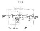
- Circuit de synchronisation permettant de synchroniser des données entre des horloges mésochrones de réception et de transmission, comprenant :caractérisé en ce que :un circuit du domaine d'horloge de réception (217) pour fournir des données synchronisées par l'horloge de réception ;un premier circuit de verrouillage (307), couplé à une sortie du circuit du domaine d'horloge de réception, pour verrouiller les données ;un second circuit de verrouillage (309) pour verrouiller les données ;un circuit de multiplexage (310), possédant des entrées couplées aux sorties des premier et deuxième circuits de verrouillage ; etun circuit de mesure de phase (401), configuré pour mesurer la différence de phase entre les horloges de réception et de transmission et pour fournir un signal de sélection au multiplexeur (310) en fonction de la différence de phase ; dans lequel l'horloge de réception et l'horloge de transmission sont mésochrones ;le premier circuit de verrouillage (307) est configuré pour verrouiller les données sur le premier front de l'horloge de transmission ;le second circuit de verrouillage (309) est configuré pour verrouiller les données sur le second front de l'horloge de transmission ; etle second circuit de verrouillage (309) est couplé aux sorties du circuit du domaine d'horloge de réception, parallèlement au premier circuit de verrouillage (307).
- Circuit de synchronisation selon la revendication 1, dans lequel le circuit de mesure de phase est configuré pour déterminer une différence de phase entre l'horloge de réception et une horloge en quadrature avec l'horloge de transmission.
- Circuit de synchronisation selon la revendication 2, dans lequel le circuit de mesure de phase comprend un comparateur de phases couplé de manière à recevoir l'horloge de réception et l'horloge en quadrature avec l'horloge de transmission, et un intégrateur couplé à une sortie du comparateur de phase ; et
le circuit de synchronisation comprenant un verrou couplé à une sortie du circuit de mesure de phase afin de verrouiller un signal de sortie après une période d'initialisation. - Circuit de synchronisation selon la revendication 2, dans lequel le circuit de mesure de phase comprend :un comparateur de phases couplé pour recevoir l'horloge de réception et l'horloge en quadrature avec l'horloge de transmission ; etun intégrateur couplé à une sortie du comparateur de phases.
- Circuit de synchronisation selon la revendication 1, 2, 3 ou 4, comprenant en outre un troisième circuit de verrouillage (308), connecté entre une sortie du premier circuit de verrouillage et le multiplexeur (310), pour réajuster le rythme de la sortie du premier circuit de verrouillage (307) au second front du signal de l'horloge de transmission.
- Circuit de synchronisation selon la revendication 3 ou 4, comprenant en outre un verrou de. signaux de sélection (403) connecté entre l'intégrateur et une entrée de sélection du multiplexeur (310).
- Circuit de synchronisation selon la revendication 3 ou 4, comprenant en outre une pluralité de verrous de signaux de sélection (431) pour stocker différents signaux de sélection correspondant aux différentes fréquences d'horloge, couplés entre l'intégrateur et une entrée de sélection du multiplexeur (310).
- Circuit de synchronisation selon l'une quelconque des revendications 1 à 7, dans lequel les premier et second circuits de verrouillage comprennent chacun un amplificateur de détection préchargé.
- Système du bus mémoire synchrone comprenant :un bus de données (202) possédant une première extrémité et une seconde extrémité ;une source d'horloge (300) générant un signal d'horloge ;une ligne d'horloge transmettant le signal d'horloge, laquelle ligne d'horloge possède :un premier segment de ligne d'horloge (200) s'étendant de la première extrémité du bus de données à un point de retournement proche de la seconde extrémité du bus de données ; etun second segment de ligne d'horloge (201) s'étendant du point de retournement à la première extrémité du bus de données ;un premier dispositif (301) couplé au bus de données pour transmettre des données à un second dispositif (302) comprenant un ensemble de circuits de synchronisation selon la revendication 1 qui reçoit l'horloge de transmission provenant de l'un des premier et second segments de ligne d'horloge, l'horloge de réception de l'autre du premier et du second segment d'horloge, et une horloge de transmission en quadrature avec l'horloge de transmission, dans lequel l'horloge de transmission et l'horloge de réception sont mésochrones.
- Procédé permettant de synchroniser des données entre des horloges de réception et de transmission mésochrones, comprenant les étapes consistant à :caractérisé par :fournir des données synchronisées par une horloge de réception à partir d'un domaine d'horloge de réception ;verrouiller les données dans un premier circuit de verrouillage (307) ;verrouiller les données dans un second circuit de verrouillage (309) ;mesurer une différence de phase entre les horloges de réception et de transmission et fournir un signal de sélection en fonction de la différence de phase ; dans lequel l'horloge de réception et l'horloge de transmission sont mésochrones ; etsélectionner l'une des sorties du premier circuit de verrouillage (307) et du second circuit de verrouillage (309) en fonction du signal de sélection ;le verrouillage des données dans le .premier circuit de verrouillage (307) sur un premier front d'une horloge de transmission ;le verrouillage des données dans le second circuit de verrouillage (309) sur un second front de l'horloge de transmission ; etla réception des données au niveau du second circuit de verrouillage (309) parallèlement à la réception des données au niveau du premier circuit de verrouillage (307).
- Procédé selon la revendication 10, dans lequel l'étape de mesure d'une différence de phase comprend la détermination d'une différence de phase entre l'horloge de réception et l'horloge en quadrature avec l'horloge de transmission.
- Procédé selon la revendication 10, dans lequel l'étape de mesure d'une différence de phase comprend les étapes consistant à :comparer l'horloge de réception et une horloge en quadrature avec l'horloge de transmission ; etintégrer un résultat de l'étape de comparaison.
- Procédé selon la revendication 10, 11 ou 12, comprenant en outre une étape de verrouillage du signal de sélection après une séquence d'initialisation ou de calibrage.
- Procédé selon la revendication 10, 11, 12 ou 13, comprenant en outre le verrouillage d'une sortie du premier circuit de verrouillage au second front du signal d'horloge de transmission de manière à réajuster le rythme de la sortie du premier circuit de verrouillage (307) au second front du signal d'horloge de transmission.
- Circuit de synchronisation permettant de synchroniser des données entre des horloges de réception et de transmission mésochrones, comprenant :caractérisé parun premier circuit du domaine d'horloge de réception pour fournir les données synchronisées par un premier front de l'horloge de réception ;un second circuit du domaine d'horloge de réception pour fournir les données synchronisées par un second front de l'horloge de réception ;deux circuits de verrouillage, pour verrouiller chacun les données à un front de l'horloge de transmission ; dans lequel l'horloge de réception et l'horloge de transmission sont mésochrones ;un circuit de multiplexage ; etun circuit de mesure de phase, configuré pour mesurer une différence de phase entre les horloges de réception et de transmission et pour fournir un signal de sélection au multiplexeur en fonction des différences de phase ;
le couplage de chacun des deux circuits de verrouillage à une sortie des dits premier et second circuits de domaine d'horloge de réception respectifs, afin de verrouiller les données à un front de l'horloge de transmission, les deux circuits de verrouillage étant connectés en parallèle entre les premier et second circuits de domaine d'horloge de réception et le circuit de multiplexage ;
le couplage des entrées du circuit de multiplexage aux sorties dès deux circuits de verrouillage ; et
la configuration du circuit de mesure de phase pour déterminer une différence de phase entre l'horloge de réception et une horloge en quadrature avec l'horloge de transmission. - Circuit de synchronisation selon la revendication 15, dans lequel le circuit de mesure de phase comprend :un comparateur de phases couplé de manière à recevoir l'horloge de réception et l'horloge en quadrature.avec l'horloge de transmission ; etun intégrateur couplé à une sortie du comparateur de phases.
Applications Claiming Priority (3)
| Application Number | Priority Date | Filing Date | Title |
|---|---|---|---|
| US6150597P | 1997-10-10 | 1997-10-10 | |
| US61505P | 1997-10-10 | ||
| PCT/US1998/021448 WO1999019806A1 (fr) | 1997-10-10 | 1998-10-09 | Procede et systeme de resynchronisation a securite integree avec temps d'attente minimal |
Publications (2)
| Publication Number | Publication Date |
|---|---|
| EP1031093A1 EP1031093A1 (fr) | 2000-08-30 |
| EP1031093B1 true EP1031093B1 (fr) | 2003-02-05 |
Family
ID=22036219
Family Applications (1)
| Application Number | Title | Priority Date | Filing Date |
|---|---|---|---|
| EP98952237A Expired - Lifetime EP1031093B1 (fr) | 1997-10-10 | 1998-10-09 | Procede et systeme de resynchronisation a securite integree avec temps d'attente minimal |
Country Status (8)
| Country | Link |
|---|---|
| US (3) | US6473439B1 (fr) |
| EP (1) | EP1031093B1 (fr) |
| JP (1) | JP4484359B2 (fr) |
| KR (1) | KR100603687B1 (fr) |
| AT (1) | ATE232317T1 (fr) |
| AU (1) | AU9798698A (fr) |
| DE (1) | DE69811262T2 (fr) |
| WO (1) | WO1999019806A1 (fr) |
Families Citing this family (95)
| Publication number | Priority date | Publication date | Assignee | Title |
|---|---|---|---|---|
| KR100603687B1 (ko) | 1997-10-10 | 2006-07-20 | 람버스 인코포레이티드 | 최소의 대기시간으로 페일-세이프 재동기화를 위한 방법및 장치 |
| US6799280B1 (en) * | 2000-01-04 | 2004-09-28 | Advanced Micro Devices, Inc. | System and method for synchronizing data transfer from one domain to another by selecting output data from either a first or second storage device |
| US20020097682A1 (en) * | 2000-06-02 | 2002-07-25 | Enam Syed K. | Low frequency loop-back in a high speed optical transceiver |
| FR2810009B1 (fr) * | 2000-06-09 | 2002-09-27 | Otico | Dispositif d'entrainement a chenille pour vehicule tout terrain |
| JP3857230B2 (ja) * | 2000-10-11 | 2006-12-13 | Nttエレクトロニクス株式会社 | 位相比較回路 |
| DE10059758A1 (de) * | 2000-11-30 | 2002-06-20 | Bosch Gmbh Robert | Verfahren zum Empfangen von Daten |
| US20020194518A1 (en) * | 2001-06-06 | 2002-12-19 | Chang Kun-Yung Ken | Apparatus and method for generating a skip signal |
| US7194056B2 (en) * | 2001-06-25 | 2007-03-20 | Rambus Inc. | Determining phase relationships using digital phase values |
| EP1446910B1 (fr) | 2001-10-22 | 2010-08-11 | Rambus Inc. | Appareil et procede de reglage de phase pour systeme de signalement a dispositif de memoire |
| TWI235917B (en) | 2002-04-15 | 2005-07-11 | Via Tech Inc | High speed data transmitter and transmission method thereof |
| CN100421096C (zh) * | 2002-05-08 | 2008-09-24 | 威盛电子股份有限公司 | 高速数据传输器及其传输方法 |
| US7149874B2 (en) * | 2002-08-16 | 2006-12-12 | Micron Technology, Inc. | Memory hub bypass circuit and method |
| US7359407B1 (en) * | 2002-08-27 | 2008-04-15 | Cypress Semiconductor Corp. | Data interface that is configurable into separate modes of operation for sub-bit de-skewing of parallel-fed data signals |
| JP3704709B2 (ja) | 2002-10-02 | 2005-10-12 | 日本電気株式会社 | データ再同期化装置 |
| US6729994B1 (en) * | 2002-10-29 | 2004-05-04 | General Motors Corporation | Multi-speed transmission mechanisms with three planetary gearsets and clutch input |
| US7231009B2 (en) * | 2003-02-19 | 2007-06-12 | Silicon Image, Inc. | Data synchronization across an asynchronous boundary using, for example, multi-phase clocks |
| US6864722B2 (en) * | 2003-05-09 | 2005-03-08 | Hewlett-Packard Development Company, L.P. | Phase detector for a programmable clock synchronizer |
| US7275171B2 (en) | 2003-05-22 | 2007-09-25 | Rambus Inc. | Method and apparatus for programmable sampling clock edge selection |
| US7133991B2 (en) * | 2003-08-20 | 2006-11-07 | Micron Technology, Inc. | Method and system for capturing and bypassing memory transactions in a hub-based memory system |
| US7072355B2 (en) * | 2003-08-21 | 2006-07-04 | Rambus, Inc. | Periodic interface calibration for high speed communication |
| US7136958B2 (en) | 2003-08-28 | 2006-11-14 | Micron Technology, Inc. | Multiple processor system and method including multiple memory hub modules |
| US7120743B2 (en) * | 2003-10-20 | 2006-10-10 | Micron Technology, Inc. | Arbitration system and method for memory responses in a hub-based memory system |
| US7073146B2 (en) * | 2003-10-30 | 2006-07-04 | Atrenta Inc. | Method for clock synchronization validation in integrated circuit design |
| KR20050076202A (ko) * | 2004-01-20 | 2005-07-26 | 삼성전자주식회사 | 지연 신호 발생 회로 및 이를 포함한 메모리 시스템 |
| US7400670B2 (en) | 2004-01-28 | 2008-07-15 | Rambus, Inc. | Periodic calibration for communication channels by drift tracking |
| US7158536B2 (en) * | 2004-01-28 | 2007-01-02 | Rambus Inc. | Adaptive-allocation of I/O bandwidth using a configurable interconnect topology |
| US7095789B2 (en) * | 2004-01-28 | 2006-08-22 | Rambus, Inc. | Communication channel calibration for drift conditions |
| US8422568B2 (en) | 2004-01-28 | 2013-04-16 | Rambus Inc. | Communication channel calibration for drift conditions |
| US7412574B2 (en) * | 2004-02-05 | 2008-08-12 | Micron Technology, Inc. | System and method for arbitration of memory responses in a hub-based memory system |
| US7788451B2 (en) | 2004-02-05 | 2010-08-31 | Micron Technology, Inc. | Apparatus and method for data bypass for a bi-directional data bus in a hub-based memory sub-system |
| FR2867334B1 (fr) * | 2004-03-05 | 2006-04-28 | Thales Sa | Procede et dispositif d'echantillonnage de donnees numeriques dans une transmission synchrone, avec maintien de l'integrite binaire |
| US6961862B2 (en) * | 2004-03-17 | 2005-11-01 | Rambus, Inc. | Drift tracking feedback for communication channels |
| US7257683B2 (en) * | 2004-03-24 | 2007-08-14 | Micron Technology, Inc. | Memory arbitration system and method having an arbitration packet protocol |
| US7447240B2 (en) * | 2004-03-29 | 2008-11-04 | Micron Technology, Inc. | Method and system for synchronizing communications links in a hub-based memory system |
| US7159199B2 (en) * | 2004-04-02 | 2007-01-02 | Stmicroelectronics Limited | Method for verifying adequate synchronization of signals that cross clock environments and system |
| US6980042B2 (en) * | 2004-04-05 | 2005-12-27 | Micron Technology, Inc. | Delay line synchronizer apparatus and method |
| US7535985B2 (en) | 2004-04-26 | 2009-05-19 | Panasonic Corporation | Resynchronization circuit |
| US20050259692A1 (en) * | 2004-05-19 | 2005-11-24 | Zerbe Jared L | Crosstalk minimization in serial link systems |
| US7978754B2 (en) * | 2004-05-28 | 2011-07-12 | Rambus Inc. | Communication channel calibration with nonvolatile parameter store for recovery |
| US7363419B2 (en) | 2004-05-28 | 2008-04-22 | Micron Technology, Inc. | Method and system for terminating write commands in a hub-based memory system |
| US7516029B2 (en) | 2004-06-09 | 2009-04-07 | Rambus, Inc. | Communication channel calibration using feedback |
| US7535958B2 (en) * | 2004-06-14 | 2009-05-19 | Rambus, Inc. | Hybrid wired and wireless chip-to-chip communications |
| US7489739B2 (en) * | 2004-09-17 | 2009-02-10 | Rambus, Inc. | Method and apparatus for data recovery |
| US20060098770A1 (en) * | 2004-11-09 | 2006-05-11 | Harper William F | Synchronizer for passing data from a first system to a second system |
| US7199728B2 (en) * | 2005-01-21 | 2007-04-03 | Rambus, Inc. | Communication system with low power, DC-balanced serial link |
| US7088270B1 (en) * | 2005-01-21 | 2006-08-08 | Rambus, Inc. | Low power, DC-balanced serial link |
| US7061406B1 (en) * | 2005-01-21 | 2006-06-13 | Rambus, Inc. | Low power, DC-balanced serial link transmitter |
| US9384818B2 (en) | 2005-04-21 | 2016-07-05 | Violin Memory | Memory power management |
| US9582449B2 (en) | 2005-04-21 | 2017-02-28 | Violin Memory, Inc. | Interconnection system |
| US8112655B2 (en) * | 2005-04-21 | 2012-02-07 | Violin Memory, Inc. | Mesosynchronous data bus apparatus and method of data transmission |
| EP2383661A1 (fr) | 2005-04-21 | 2011-11-02 | Violin Memory, Inc. | Système d'interconnexion |
| US7332950B2 (en) * | 2005-06-14 | 2008-02-19 | Micron Technology, Inc. | DLL measure initialization circuit for high frequency operation |
| US9420332B2 (en) * | 2006-07-06 | 2016-08-16 | Qualcomm Incorporated | Clock compensation techniques for audio decoding |
| US7653167B2 (en) * | 2006-09-07 | 2010-01-26 | Intel Corporation | Phase deglitch circuit for phase interpolator for high-speed serial I/O applications |
| EP1901474B1 (fr) | 2006-09-13 | 2011-11-30 | Stmicroelectronics Sa | Système de synchronisation de modules dans un circuit intégré dans des domaines d'horloge mésochrones |
| US20080109672A1 (en) * | 2006-11-08 | 2008-05-08 | Sicortex, Inc | Large scale computing system with multi-lane mesochronous data transfers among computer nodes |
| EP1936857A1 (fr) * | 2006-12-22 | 2008-06-25 | Stmicroelectronics Sa | Système de transmission de données entre un module transmetteur et un module récepteur sur un canal fourni avec un lien de contrôle de flux |
| US7836324B2 (en) * | 2007-02-09 | 2010-11-16 | Apple Inc. | Oversampling-based scheme for synchronous interface communication |
| US7904859B2 (en) * | 2007-05-09 | 2011-03-08 | Synopsys, Inc. | Method and apparatus for determining a phase relationship between asynchronous clock signals |
| US7984400B2 (en) * | 2007-05-09 | 2011-07-19 | Synopsys, Inc. | Techniques for use with automated circuit design and simulations |
| US8756557B2 (en) * | 2007-05-09 | 2014-06-17 | Synopsys, Inc. | Techniques for use with automated circuit design and simulations |
| US7908574B2 (en) * | 2007-05-09 | 2011-03-15 | Synopsys, Inc. | Techniques for use with automated circuit design and simulations |
| US7619449B2 (en) * | 2007-06-07 | 2009-11-17 | Micron Technology, Inc. | Method and apparatus for synchronous clock distribution to a plurality of destinations |
| KR100929824B1 (ko) * | 2008-05-06 | 2009-12-07 | 주식회사 하이닉스반도체 | 반도체 소자 |
| JP5276928B2 (ja) * | 2008-08-29 | 2013-08-28 | 株式会社日立製作所 | 信号再生回路向け位相比較回路及び信号再生回路向け位相比較回路を備える光通信装置 |
| US8181056B2 (en) * | 2008-09-30 | 2012-05-15 | Mosaid Technologies Incorporated | Serial-connected memory system with output delay adjustment |
| US8161313B2 (en) * | 2008-09-30 | 2012-04-17 | Mosaid Technologies Incorporated | Serial-connected memory system with duty cycle correction |
| EP2427184B1 (fr) | 2009-05-08 | 2017-08-30 | 3M Innovative Properties Company | Procédé et kit d'hygiène buccale |
| CN102460972B (zh) * | 2009-06-30 | 2015-10-14 | 拉姆伯斯公司 | 用于调整时钟信号以补偿噪声的方法、系统和集成电路 |
| US9465756B2 (en) * | 2009-12-23 | 2016-10-11 | Violin Memory Inc. | Configurable interconnection system |
| US8261121B2 (en) * | 2009-12-24 | 2012-09-04 | Nvidia Corporation | Command latency reduction and command bandwidth maintenance in a memory circuit |
| US8707080B1 (en) * | 2011-07-12 | 2014-04-22 | Emc Corporation | Simple circular asynchronous clock domain crossing technique for digital data |
| US8415981B2 (en) * | 2011-08-15 | 2013-04-09 | Mediatek Singapore Pte. Ltd. | Integrated circuit device, synchronisation module, electronic device and method therefor |
| US8782458B2 (en) * | 2011-11-29 | 2014-07-15 | Advanced Micro Devices, Inc. | System and method of data communications between electronic devices |
| CN103247323B (zh) * | 2012-02-07 | 2016-05-04 | 北京兆易创新科技股份有限公司 | 一种串行接口快闪存储器 |
| CN103247325B (zh) * | 2012-02-07 | 2017-03-01 | 北京兆易创新科技股份有限公司 | 一种串行i/o接口快闪存储器 |
| US8836394B2 (en) | 2012-03-26 | 2014-09-16 | Rambus Inc. | Method and apparatus for source-synchronous signaling |
| TWI449338B (zh) * | 2012-04-18 | 2014-08-11 | Univ Nat Sun Yat Sen | 具數位校正之峰值偵測器 |
| KR101950320B1 (ko) * | 2012-06-29 | 2019-02-20 | 에스케이하이닉스 주식회사 | 위상 검출 회로 및 이를 이용한 동기 회로 |
| US8760204B2 (en) * | 2012-11-20 | 2014-06-24 | Nvidia Corporation | Variation-tolerant periodic synchronizer |
| JP5826971B2 (ja) * | 2013-04-22 | 2015-12-02 | シャープ株式会社 | スタイラスペン、タッチパネルシステム、および電子機器 |
| US9213487B2 (en) | 2013-10-16 | 2015-12-15 | Qualcomm Incorporated | Receiver architecture for memory reads |
| KR102248279B1 (ko) * | 2014-06-13 | 2021-05-07 | 삼성전자주식회사 | 불휘발성 메모리 및 메모리 컨트롤러를 포함하는 스토리지 장치, 그리고 불휘발성 메모리 및 메모리 컨트롤러 사이의 통신을 중개하는 리타이밍 회로의 동작 방법 |
| US10481203B2 (en) * | 2015-04-04 | 2019-11-19 | Nvidia Corporation | Granular dynamic test systems and methods |
| US9541990B2 (en) | 2015-04-21 | 2017-01-10 | Cypress Semiconductor Corporation | Asynchronous transceiver for on-vehicle electronic device |
| US10444280B2 (en) | 2015-10-27 | 2019-10-15 | Nvidia Corporation | Independent test partition clock coordination across multiple test partitions |
| US10095263B1 (en) * | 2015-12-15 | 2018-10-09 | Marvell International Ltd. | Apparatus and method for calibrating signal synchronization |
| US10623174B1 (en) | 2018-12-12 | 2020-04-14 | Xilinx, Inc. | Low latency data transfer technique for mesochronous divided clocks |
| CN112088523B (zh) * | 2019-03-27 | 2023-04-28 | 京东方科技集团股份有限公司 | 物联网系统、中央控制设备、应用设备以及通信方法 |
| CN111797043B (zh) * | 2019-04-08 | 2022-04-26 | 达发科技(苏州)有限公司 | 跨时脉域系统 |
| US10924091B2 (en) * | 2019-07-02 | 2021-02-16 | Stmicroelectronics International N.V. | Immediate fail detect clock domain crossing synchronizer |
| US10965441B1 (en) * | 2019-10-10 | 2021-03-30 | Rohde & Schwarz Gmbh & Co. Kg | Frame trigger recreation method and frame trigger recreator |
| DE112020007048T5 (de) * | 2020-04-09 | 2023-03-30 | Advantest Corporation | Schaltung zum transferieren von daten von einer taktdomain zu einer anderen |
| US11829640B2 (en) | 2020-10-27 | 2023-11-28 | Rambus Inc. | Asynchronous arbitration across clock domains for register writes in an integrated circuit chip |
| US11677391B1 (en) * | 2021-01-28 | 2023-06-13 | Rambus Inc. | Low-power multi-domain synchronizer |
Family Cites Families (26)
| Publication number | Priority date | Publication date | Assignee | Title |
|---|---|---|---|---|
| US4819081A (en) * | 1987-09-03 | 1989-04-04 | Intel Corporation | Phase comparator for extending capture range |
| US5551050A (en) | 1989-12-20 | 1996-08-27 | Texas Instruments Incorporated | System and method using synchronized processors to perform real time internal monitoring of a data processing device |
| JPH04262618A (ja) * | 1991-02-18 | 1992-09-18 | Advantest Corp | 位相検波器 |
| DE4345604B3 (de) * | 1992-03-06 | 2012-07-12 | Rambus Inc. | Vorrichtung zur Kommunikation mit einem DRAM |
| JPH06132972A (ja) * | 1992-10-20 | 1994-05-13 | Fujitsu Ltd | 広帯域isdn遠隔多重装置 |
| US5757868A (en) * | 1994-02-16 | 1998-05-26 | Motorola, Inc. | Digital phase detector with integrated phase detection |
| US5509038A (en) * | 1994-04-06 | 1996-04-16 | Hal Computer Systems, Inc. | Multi-path data synchronizer system and method |
| US5550875A (en) | 1994-12-29 | 1996-08-27 | Unisys Corporation | Apparatus and method for residual error clock skew bound, and clocking therewith |
| US5646519A (en) * | 1995-06-07 | 1997-07-08 | Symmetricom, Inc. | Digital phase detector employing a digitally controllable delay line |
| JP3873089B2 (ja) | 1995-06-07 | 2007-01-24 | 三星電子株式会社 | 互いに非同期の2つのバス間でデータ転送を同期する際の累積時間遅延を低減するもの |
| US5652530A (en) | 1995-09-29 | 1997-07-29 | Intel Corporation | Method and apparatus for reducing clock-data skew by clock shifting |
| JP2806863B2 (ja) * | 1996-02-27 | 1998-09-30 | 日本電気エンジニアリング株式会社 | ビット同期回路 |
| US5799048A (en) * | 1996-04-17 | 1998-08-25 | Sun Microsystems, Inc. | Phase detector for clock synchronization and recovery |
| JP3467975B2 (ja) * | 1996-06-27 | 2003-11-17 | 安藤電気株式会社 | 位相検出回路 |
| US6205191B1 (en) * | 1997-07-21 | 2001-03-20 | Rambus Inc. | Method and apparatus for synchronizing a control signal |
| US6008680A (en) * | 1997-08-27 | 1999-12-28 | Lsi Logic Corporation | Continuously adjustable delay-locked loop |
| KR100603687B1 (ko) | 1997-10-10 | 2006-07-20 | 람버스 인코포레이티드 | 최소의 대기시간으로 페일-세이프 재동기화를 위한 방법및 장치 |
| TW388795B (en) * | 1997-12-24 | 2000-05-01 | Via Tech Inc | Auxiliary device and method for signal testing |
| US6150889A (en) * | 1998-08-03 | 2000-11-21 | Motorola, Inc. | Circuit and method for minimizing recovery time |
| US6334163B1 (en) * | 1999-03-05 | 2001-12-25 | International Business Machines Corp. | Elastic interface apparatus and method therefor |
| US6100722A (en) * | 1999-07-28 | 2000-08-08 | Cypress Semiconductor Corp. | Phase detector with extended linear range |
| US6172540B1 (en) * | 1999-08-16 | 2001-01-09 | Intel Corporation | Apparatus for fast logic transfer of data across asynchronous clock domains |
| US6799280B1 (en) * | 2000-01-04 | 2004-09-28 | Advanced Micro Devices, Inc. | System and method for synchronizing data transfer from one domain to another by selecting output data from either a first or second storage device |
| US6987823B1 (en) * | 2000-02-07 | 2006-01-17 | Rambus Inc. | System and method for aligning internal transmit and receive clocks |
| US6798259B2 (en) * | 2001-08-03 | 2004-09-28 | Micron Technology, Inc. | System and method to improve the efficiency of synchronous mirror delays and delay locked loops |
| US6614314B2 (en) * | 2001-12-03 | 2003-09-02 | Gennum Corporation | Non-linear phase detector |
-
1998
- 1998-10-09 KR KR1020007003852A patent/KR100603687B1/ko not_active IP Right Cessation
- 1998-10-09 AU AU97986/98A patent/AU9798698A/en not_active Abandoned
- 1998-10-09 JP JP2000516290A patent/JP4484359B2/ja not_active Expired - Lifetime
- 1998-10-09 WO PCT/US1998/021448 patent/WO1999019806A1/fr active IP Right Grant
- 1998-10-09 EP EP98952237A patent/EP1031093B1/fr not_active Expired - Lifetime
- 1998-10-09 DE DE69811262T patent/DE69811262T2/de not_active Expired - Fee Related
- 1998-10-09 US US09/169,372 patent/US6473439B1/en not_active Expired - Fee Related
- 1998-10-09 AT AT98952237T patent/ATE232317T1/de not_active IP Right Cessation
-
2002
- 2002-10-28 US US10/282,531 patent/US6949958B2/en not_active Expired - Fee Related
-
2005
- 2005-09-27 US US11/237,276 patent/US7288973B2/en not_active Expired - Fee Related
Also Published As
| Publication number | Publication date |
|---|---|
| DE69811262T2 (de) | 2003-11-27 |
| US6949958B2 (en) | 2005-09-27 |
| KR20010031036A (ko) | 2001-04-16 |
| US7288973B2 (en) | 2007-10-30 |
| US20030053489A1 (en) | 2003-03-20 |
| US6473439B1 (en) | 2002-10-29 |
| KR100603687B1 (ko) | 2006-07-20 |
| DE69811262D1 (de) | 2003-03-13 |
| US20060022724A1 (en) | 2006-02-02 |
| EP1031093A1 (fr) | 2000-08-30 |
| WO1999019806A1 (fr) | 1999-04-22 |
| ATE232317T1 (de) | 2003-02-15 |
| JP4484359B2 (ja) | 2010-06-16 |
| JP2001520417A (ja) | 2001-10-30 |
| AU9798698A (en) | 1999-05-03 |
Similar Documents
| Publication | Publication Date | Title |
|---|---|---|
| EP1031093B1 (fr) | Procede et systeme de resynchronisation a securite integree avec temps d'attente minimal | |
| US7974375B2 (en) | Linear phase detector and clock/data recovery circuit thereof | |
| US7571340B2 (en) | Eliminating receiver clock drift caused by voltage and temperature change in a high-speed I/O system that uses a forwarded clock | |
| JP4065234B2 (ja) | 同期式チップーチップシステムのデータリカバリ装置 | |
| US7765074B2 (en) | Circuit, apparatus and method for capturing a representation of a waveform from a clock-data recovery (CDR) unit | |
| US11061432B2 (en) | Data handoff between two clock domains sharing a fundamental beat | |
| US7978802B1 (en) | Method and apparatus for a mesochronous transmission system | |
| US7256627B1 (en) | Alignment of local transmit clock to synchronous data transfer clock having programmable transfer rate | |
| US7170964B2 (en) | Transition insensitive timing recovery method and apparatus | |
| KR920003831B1 (ko) | 안정된 데이타 전송 방법 및 장치 | |
| US5689530A (en) | Data recovery circuit with large retime margin | |
| US6795514B2 (en) | Integrated data clock extractor | |
| US7519844B2 (en) | PVT drift compensation | |
| US7583118B2 (en) | Delay locked loop circuit | |
| US6724846B1 (en) | Simple, high performance, bit-sliced mesochronous synchronizer for a source synchronous link | |
| US7430141B2 (en) | Method and apparatus for memory data deskewing | |
| JP3415891B2 (ja) | パケットデータ再生システム | |
| US7231009B2 (en) | Data synchronization across an asynchronous boundary using, for example, multi-phase clocks | |
| US8718215B2 (en) | Method and apparatus for deskewing data transmissions | |
| Schell et al. | A 3-12.5 Gb/s Reference-Less CDR for an Eye-Opening Monitor | |
| Brandon | Synchronizing multiple AD9852 DDS-based synthesizers |
Legal Events
| Date | Code | Title | Description |
|---|---|---|---|
| PUAI | Public reference made under article 153(3) epc to a published international application that has entered the european phase |
Free format text: ORIGINAL CODE: 0009012 |
|
| 17P | Request for examination filed |
Effective date: 20000510 |
|
| AK | Designated contracting states |
Kind code of ref document: A1 Designated state(s): AT BE CH DE FR GB IE IT LI LU NL |
|
| RAP1 | Party data changed (applicant data changed or rights of an application transferred) |
Owner name: RAMBUS INC. |
|
| 17Q | First examination report despatched |
Effective date: 20011025 |
|
| GRAH | Despatch of communication of intention to grant a patent |
Free format text: ORIGINAL CODE: EPIDOS IGRA |
|
| GRAH | Despatch of communication of intention to grant a patent |
Free format text: ORIGINAL CODE: EPIDOS IGRA |
|
| GRAA | (expected) grant |
Free format text: ORIGINAL CODE: 0009210 |
|
| AK | Designated contracting states |
Designated state(s): AT BE CH DE FR GB IE IT LI LU NL |
|
| PG25 | Lapsed in a contracting state [announced via postgrant information from national office to epo] |
Ref country code: NL Free format text: LAPSE BECAUSE OF FAILURE TO SUBMIT A TRANSLATION OF THE DESCRIPTION OR TO PAY THE FEE WITHIN THE PRESCRIBED TIME-LIMIT Effective date: 20030205 Ref country code: LI Free format text: LAPSE BECAUSE OF FAILURE TO SUBMIT A TRANSLATION OF THE DESCRIPTION OR TO PAY THE FEE WITHIN THE PRESCRIBED TIME-LIMIT Effective date: 20030205 Ref country code: CH Free format text: LAPSE BECAUSE OF FAILURE TO SUBMIT A TRANSLATION OF THE DESCRIPTION OR TO PAY THE FEE WITHIN THE PRESCRIBED TIME-LIMIT Effective date: 20030205 Ref country code: BE Free format text: LAPSE BECAUSE OF FAILURE TO SUBMIT A TRANSLATION OF THE DESCRIPTION OR TO PAY THE FEE WITHIN THE PRESCRIBED TIME-LIMIT Effective date: 20030205 Ref country code: AT Free format text: LAPSE BECAUSE OF FAILURE TO SUBMIT A TRANSLATION OF THE DESCRIPTION OR TO PAY THE FEE WITHIN THE PRESCRIBED TIME-LIMIT Effective date: 20030205 |
|
| REG | Reference to a national code |
Ref country code: GB Ref legal event code: FG4D |
|
| REG | Reference to a national code |
Ref country code: CH Ref legal event code: EP |
|
| REG | Reference to a national code |
Ref country code: IE Ref legal event code: FG4D |
|
| REF | Corresponds to: |
Ref document number: 69811262 Country of ref document: DE Date of ref document: 20030313 Kind code of ref document: P |
|
| NLV1 | Nl: lapsed or annulled due to failure to fulfill the requirements of art. 29p and 29m of the patents act | ||
| REG | Reference to a national code |
Ref country code: CH Ref legal event code: PL |
|
| ET | Fr: translation filed | ||
| PG25 | Lapsed in a contracting state [announced via postgrant information from national office to epo] |
Ref country code: LU Free format text: LAPSE BECAUSE OF NON-PAYMENT OF DUE FEES Effective date: 20031009 Ref country code: IE Free format text: LAPSE BECAUSE OF NON-PAYMENT OF DUE FEES Effective date: 20031009 |
|
| PLBE | No opposition filed within time limit |
Free format text: ORIGINAL CODE: 0009261 |
|
| STAA | Information on the status of an ep patent application or granted ep patent |
Free format text: STATUS: NO OPPOSITION FILED WITHIN TIME LIMIT |
|
| 26N | No opposition filed |
Effective date: 20031106 |
|
| REG | Reference to a national code |
Ref country code: IE Ref legal event code: MM4A |
|
| PGFP | Annual fee paid to national office [announced via postgrant information from national office to epo] |
Ref country code: GB Payment date: 20041006 Year of fee payment: 7 |
|
| PGFP | Annual fee paid to national office [announced via postgrant information from national office to epo] |
Ref country code: FR Payment date: 20041020 Year of fee payment: 7 |
|
| PGFP | Annual fee paid to national office [announced via postgrant information from national office to epo] |
Ref country code: DE Payment date: 20041130 Year of fee payment: 7 |
|
| PG25 | Lapsed in a contracting state [announced via postgrant information from national office to epo] |
Ref country code: IT Free format text: LAPSE BECAUSE OF NON-PAYMENT OF DUE FEES Effective date: 20051009 Ref country code: GB Free format text: LAPSE BECAUSE OF NON-PAYMENT OF DUE FEES Effective date: 20051009 |
|
| PG25 | Lapsed in a contracting state [announced via postgrant information from national office to epo] |
Ref country code: DE Free format text: LAPSE BECAUSE OF NON-PAYMENT OF DUE FEES Effective date: 20060503 |
|
| GBPC | Gb: european patent ceased through non-payment of renewal fee |
Effective date: 20051009 |
|
| PG25 | Lapsed in a contracting state [announced via postgrant information from national office to epo] |
Ref country code: FR Free format text: LAPSE BECAUSE OF NON-PAYMENT OF DUE FEES Effective date: 20060630 |
|
| REG | Reference to a national code |
Ref country code: FR Ref legal event code: ST Effective date: 20060630 |