EP1025448B1 - Monolithischer magnetischer sensor mit extern einstellbarer temperaturkompensation - Google Patents
Monolithischer magnetischer sensor mit extern einstellbarer temperaturkompensation Download PDFInfo
- Publication number
- EP1025448B1 EP1025448B1 EP98939956A EP98939956A EP1025448B1 EP 1025448 B1 EP1025448 B1 EP 1025448B1 EP 98939956 A EP98939956 A EP 98939956A EP 98939956 A EP98939956 A EP 98939956A EP 1025448 B1 EP1025448 B1 EP 1025448B1
- Authority
- EP
- European Patent Office
- Prior art keywords
- hall
- temperature
- effect device
- voltage
- component
- Prior art date
- Legal status (The legal status is an assumption and is not a legal conclusion. Google has not performed a legal analysis and makes no representation as to the accuracy of the status listed.)
- Expired - Lifetime
Links
- 230000005355 Hall effect Effects 0.000 claims description 160
- 230000035945 sensitivity Effects 0.000 claims description 30
- 230000001419 dependent effect Effects 0.000 claims description 22
- 230000008859 change Effects 0.000 claims description 14
- 238000000034 method Methods 0.000 claims description 10
- 230000000694 effects Effects 0.000 claims description 7
- 230000007423 decrease Effects 0.000 claims description 6
- 230000008878 coupling Effects 0.000 claims description 5
- 238000010168 coupling process Methods 0.000 claims description 5
- 238000005859 coupling reaction Methods 0.000 claims description 5
- 230000006903 response to temperature Effects 0.000 claims description 3
- 230000004044 response Effects 0.000 claims 8
- 239000004020 conductor Substances 0.000 description 30
- 238000010586 diagram Methods 0.000 description 16
- 239000003990 capacitor Substances 0.000 description 9
- 238000009792 diffusion process Methods 0.000 description 6
- 239000000758 substrate Substances 0.000 description 6
- 239000010409 thin film Substances 0.000 description 4
- 239000004065 semiconductor Substances 0.000 description 3
- 230000004075 alteration Effects 0.000 description 2
- 230000006872 improvement Effects 0.000 description 2
- 238000012986 modification Methods 0.000 description 2
- 230000004048 modification Effects 0.000 description 2
- 230000008569 process Effects 0.000 description 2
- 230000002411 adverse Effects 0.000 description 1
- 230000000295 complement effect Effects 0.000 description 1
- 239000010408 film Substances 0.000 description 1
- 230000036039 immunity Effects 0.000 description 1
- 238000004519 manufacturing process Methods 0.000 description 1
- 239000000463 material Substances 0.000 description 1
- 229910044991 metal oxide Inorganic materials 0.000 description 1
- 150000004706 metal oxides Chemical class 0.000 description 1
- 230000009467 reduction Effects 0.000 description 1
- 238000009966 trimming Methods 0.000 description 1
Images



Classifications
-
- G—PHYSICS
- G01—MEASURING; TESTING
- G01R—MEASURING ELECTRIC VARIABLES; MEASURING MAGNETIC VARIABLES
- G01R33/00—Arrangements or instruments for measuring magnetic variables
- G01R33/02—Measuring direction or magnitude of magnetic fields or magnetic flux
- G01R33/06—Measuring direction or magnitude of magnetic fields or magnetic flux using galvano-magnetic devices
- G01R33/07—Hall effect devices
- G01R33/072—Constructional adaptation of the sensor to specific applications
- G01R33/075—Hall devices configured for spinning current measurements
-
- G—PHYSICS
- G01—MEASURING; TESTING
- G01R—MEASURING ELECTRIC VARIABLES; MEASURING MAGNETIC VARIABLES
- G01R33/00—Arrangements or instruments for measuring magnetic variables
- G01R33/02—Measuring direction or magnitude of magnetic fields or magnetic flux
- G01R33/06—Measuring direction or magnitude of magnetic fields or magnetic flux using galvano-magnetic devices
- G01R33/07—Hall effect devices
Definitions
- the present invention relates to magnetic sensors and, more particularly, to a Hall-effect sensor arrangement having temperature compensation circuitry that is user-adjustable.
- Hall-effect elements are used to sense magnetic fields.
- a monolithically fabricated Hall-effect element employs a square plate formed, for example, of an epitaxial (epi) pocket formed in a bipolar (BP) or bipolar complementary metal oxide semiconductor (BiCMOS) process.
- the square plate has two pairs of contacts oriented such that each pair of contacts straddles the plate from a different pair of its diametrically opposing corners.
- a current I H is caused to flow between one of the two pairs of contacts, a voltage V H will appear across the other pair of contacts.
- a Hall plate may be used to measure the strength of a magnetic field B by applying a known current I H between one pair of contacts of a Hall plate and measuring the voltage V H across the other pair of contacts.
- Hall-effect elements often are used to sense the permanent magnetic fields of components.
- a Hall-effect element may be used to sense the position of a magnetic component while it is rotating or otherwise in motion relative to the Hall-effect element. Because the magnitude of a magnetic field emanating from a magnetic component changes as the temperature of the component changes, for any given position of the component with respect to the Hall-effect element, the magnitude of the output voltage V H of the Hall-effect element when the component is at a first temperature will not be the same as the output voltage V H when the component is at a second temperature. Therefore, the magnitude of the output voltage V H of a Hall-effect element does not provide a reliable indication of the position of a magnetic component when the component is subjected to a variable-temperature environment.
- a Hall-effect device comprises a Hall-effect element having at least one input for receiving a bias signal and at least one output for providing an output signal dependent on the bias signal and on a magnetic field intercepting the Hall-effect element; at least one output lead to provide an output signal responsive to the output signal of the Hall-effect element and dependent on an overall gain of the Hall-effect device; and a temperature-variable gain control circuit coupled to the Hall-effect element to adjust the sensitivity of the overall gain of the Hall-effect device to temperature changes, wherein the temperature-variable gain control circuit includes a pair of nodes such that, when a first component is coupled between the pair of nodes, changing a characteristic of only the first component alters the sensitivity of the overall gain of the Hall-effect device to temperature changes without substantially altering the overall gain of the Hall-effect device when the Hall-effect device is maintained at a reference temperature.
- a Hall effect device includes a substrate mounted within an integrated circuit package, a Hall-effect element integrated on the substrate, and a pair of terminals adapted to interface with a component external to the package.
- the pair of terminals is arranged with respect to the Hall-effect element such that, when the component is coupled to the pair of terminals, a characteristic of the component may be changed to adjust the sensitivity of the gain of the Hall effect device to temperature changes in the device.
- the Hall effect device includes a temperature-variable signal source arranged to provide the bias signal such that a value of the bias signal changes in response to temperature changes in the Hall-effect element.
- the pair of terminals is arranged with respect to the signal source such that, when the component is coupled to the pair of terminals, the characteristic of the component may be changed to adjust the sensitivity of the signal source to temperature changes in the Hall-effect element.
- a Hall-effect device includes an integrated circuit package having a Hall-effect element mounted within it, and a user-accessible component arranged with respect to the Hall-effect element such that a characteristic of the component may be changed to adjust the sensitivity of the gain of the Hall-effect device to temperature changes in the device.
- a Hall-effect device includes a Hall effect device mounted in an integrated circuit package and means for adjusting the sensitivity of the gain of the Hall-effect device to changing temperature conditions from a point external to the package.
- a method for compensating for the effects of temperature variations on a Hall-effect element comprises steps of (a) providing a Hall-effect device including a Hall-effect element and a temperature-variable gain control circuit coupled to the Hall-effect element to adjust the sensitivity of the gain of the Hall-effect device to temperature changes; the method further comprising (b) coupling a first component between a pair of nodes of the temperature-variable gain control circuit to set the sensitivity of the gain of the Hall-effect device to temperature variations; and (c) altering a characteristic of only the first component to adjust the sensitivity of the gain of the Hall-effect device to temperature variations without substantially altering the gain of the Hall-effect device when the Hall-effect device is maintained at a reference temperature.
- a method for compensating for the effects of temperature variations on a Hall-effect element includes coupling a component to a pair of external terminals of an integrated circuit to adjust the sensitivity of the gain of a Hall-effect device included in the integrated circuit.
- Figure 1 is a top-view of a quad-cell Hall-effect element 20 used in one embodiment of the invention.
- quad-cell Hall-effect element 20 includes four Hall cells 20A-20D.
- Hall cells 20A, 20B, 20C and 20D are made of n-type epitaxial (n-epi) regions (e.g., 200 micrometers in diameter) formed within p-type wells or hubs (p-wells/p-tubs) 30A, 30B, 30C and 30D, respectively.
- p-wells/p-tubs 30A, 30B, 30C and 30D are formed on an n-type substrate 32.
- Hall cells 20A, 20B, 20C and 20D includes two pairs of orthogonally oriented contacts.
- Hall cells 20A, 20B, 20C and 20D include, respectively, first pairs of contacts 20A1 and 20A3, 20B1 and 20B3, 20C1 and 20C3, and 20D1 and 20D3, and second pairs of contacts 20A2 and 20A4, 20B2 and 20B4, 20C2 and 20C4, and 20D2 and 20D4.
- Conductor 34 interconnects contacts 20A1, 20B2, 20C3 and 20D4, conductor 36 interconnects contacts 20A2, 20B3, 20C4 and 20D1, conductor 38 interconnects contacts 20A4, 20B1, 20C2 and 20D3, and conductor 40 interconnects contacts 20A3, 20B4, 20C1 and 20D2, thereby wiring cells 20A-20D in parallel such that each of cells 20A-20D is oriented orthogonally with respect to the other cells in quad-cell Hall-effect element 20. This orientation of cells 20A-20D reduces the adverse effects of imperfections, such as processing gradients, in the cells.
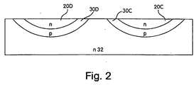
- Figure 2 is a side cross-sectional view of the substrate portion of the quad-cell Hall-effect element 20 shown in Figure 1.
- p-wells/p-tubs 30D and 30C are formed within an n-type substrate 32
- n-EPI Hall cells 20C and 20D are formed within p-wells/p-tubs 30C and 30D, respectively.
- the letters "p" and "n” in Figures 1 and 2 are intended only to illustrate the doping types of the various regions, and are not intended to signify the amounts by which the regions are doped or the process by which the regions were formed.
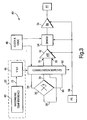
- FIG. 3 is a block diagram of one embodiment of a Hall-effect device 80 according to the invention.
- Hall-effect device 80 includes quad-cell Hall-effect element 20, commutation switches 50, a differential pre-amplifier 52, a demodulator 54, an output amplifier 56, an output terminal P7, a reference terminal P5, a temperature-variable current source 22 (which includes a ratiometric temperature reference block 42 and a voltage-to-current converter 46), and a clock and logic stage 48.
- temperature-variable current source 22 supplies a Hall bias current I H which varies according to the temperature of the device to commutation switches 50.
- Commutation switches 50 are controlled by clock and logic stage 48 to commutate the current I H alternately (1) between conductors 34 and 40, and (2) between conductors 36 and 38.
- commutation switches 50 When the current I H is presented between conductors 34 and 40, commutation switches 50 concurrently apply the voltage generated between conductors 36 and 38 (responsive to the magnetic field B ) to inputs 26 and 28, respectively, of differential pre-amplifier 52; and when the current I H is presented between conductors 36 and 38, commutation switches 50 concurrently apply the voltage generated between conductors 34 and 40 (responsive to the magnetic field B ) to inputs 26 and 28, respectively, of differential pre-amplifier 52.
- This commutation of signals to and from quad-cell Hall-effect element 20 is performed to eliminate the inherent voltage offset V OH of the Hall cells, and is discussed in detail in several of the documents referred to and incorporated by reference above.
- V OH1 V OH
- a subtraction of the voltage V 2 generated by the current flowing in the second direction from the voltage V 1 generated by the current flowing in the first direction i.e., (V H1 + V OH1 ) - (-V H2 + V OH2 )) effectively cancels the offset voltage so that only a voltage equal to 2V H results.
- this subtraction is performed by a combination of pre-amplifier 52 and demodulator 54.
- the offset-free output of demodulator 54 then is provided to the input of rail-to-rail output amplifier 56, and the output of amplifier 56 feeds external terminal P7 (e.g., a pin) of the device.
- P7 e.g., a pin
- the gain of amplifier 56 is adjusted using resistors external to device 80.
- the output voltage V H therefore always will be the same for a given magnitude of magnetic field B, regardless of the temperature of the Hall-effect device 80.
- an increase or decrease in the magnetic field strength B of a magnetic component being sensed by device 80 due to a temperature change may be countered by a corresponding decrease or increase, respectively, in the Hall current I H .
- This is useful when the magnetic field is produced by a moving permanent magnet.
- the output voltage V H of Hall-effect device 80 always will be the same when the moving (e.g., rotating) component being sensed is a given distance from device 80.
- FIG. 4 is a partial schematic/partial block diagram showing commutation switches 50 and their surrounding circuitry in more detail.
- commutation switches 50 include switches S1-S8.
- Switches S1 and S2 are connected between a first polarity output of temperature-variable current source 22 and conductors 36 and 34, respectively, of quad-cell Hall-effect element 20, and switches S3 and S4 are connected between a second polarity output of temperature-variable current source 22 and conductors 38 and 40, respectively, of Hall-effect element 20.
- switches S5 and S6 are connected, respectively, between conductors 34 and 36 of Hall-effect element 20 and non-inverting input 26 of pre-amplifier 52
- switches S7 and S8 are connected, respectively, between conductors 40 and 38 of Hall-effect element 20 and inverting input 28 of pre-amplifier 52.
- the symbol "P1" or "P2" next to switches S1-S8 indicates which of two phases of a control signal from clock and logic stage 48 (shown in Figure 3) causes each of the switches to close.
- pre-amplifier 52 receives a reference voltage V REF from reference conductor 58.
- the high-supply voltage VCC is approximately 5 volts, so the reference voltage V REF is set to approximately 2.5 volts.
- FIG. 5 is a partial schematic/partial block diagram showing demodulation block 54 in more detail.
- demodulation block 54 includes capacitors C1 and C2 and switches S9 and S10.
- Capacitor C1 is connected between a single-ended output of differential pre-amplifier 52 and one terminal of each of switches S9 and S10.
- the other terminal of switch S9 is connected to reference conductor 58 (which is maintained at V REF ), and the other terminal of switch S10 is connected to a non-inverting input of output amplifier 56.
- Capacitor C2 is connected between the non-inverting input of amplifier 56 and conductor 58.
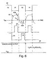
- Figure 6 is a timing diagram showing control signals for switches S1-S10 and output signals of pre-amplifier 52 and demodulator 54 shown in Figures 4 and 5.
- the timing diagram of Figure 6 illustrates: (1) commutation clock signal 60, (2) pre-amplifier output signal 62, (3) switch S10 control signal 64, (4) switch S9 control signal 66, and (5) demodulator output signal 68.
- the vertical axis of each of these signals represents an amplitude attained by the signal and the horizontal axis represents time. While all of the signals shown in Figure 6 share a common time axis, the placement of one signal above another is not intended to indicate that the signal attains a higher amplitude than do the others.
- commutation clock 60 has two phases, P1 and P2. Specifically, when clock 60 is low, it is in phase P1, and when clock 60 is high, it is in phase P2.
- switches S1-S8 is arranged to be closed during only one of these two phases. That is, switches S2, S4, S6 and S8 are closed during phase P1 (when clock 60 is low) and switches S1, S3, S5 and S7 are closed during phase P2 (when clock 60 is high).
- the phase during which each of the switches is closed is indicated next to the switch by the symbol "P1" or "P2.”
- phase P1 of clock 60 temperature-variable current source 22 is connected between conductors 34 and 40 of Hall-effect element 20 and conductors 36 and 38 of Hall-effect element 20 are connected, respectively, to non-inverting input 26 and inverting input 28 of differential pre-amplifier 52.
- Pre-amplifier 52 amplifies the differential voltage between its non-inverting input 26 and its inverting input 28, and effectively adds the amplified input voltage (which is positive during phase P1) to the reference voltage V REF on conductor 58.
- Pre-amplifier 52 then provides this sum of voltages as a single-ended output signal (shown as pre-amplifier output signal 62 in Figure 6). As shown, pre-amplifier output signal 62 is greater than V REF during phase P1 (e.g., as indicated by portion 62A of curve 62).
- phase P2 of clock 60 temperature-variable current source 22 is connected between conductors 36 and 38 of Hall-effect element 20 and conductors 34 and 40 of Hall-effect element 20 are connected, respectively, to non-inverting input 26 and inverting input 28 of differential pre-amplifier 52.
- Pre-amplifier 52 amplifies the differential voltage between its non-inverting input 26 and its inverting input 28, and effectively adds the amplified input voltage (which is negative during phase P2) to the reference voltage V REF on conductor 58.
- Pre-amplifier 52 then provides this sum of voltages as a single-ended output signal (shown as pre-amplifier output signal 62 in Figure 6). As shown, pre-amplifier output signal 62 is less than V REF during phase P2 (e.g., as indicated by portion 62B of curve 62).
- Demodulator 54 deals with this difference by effectively subtracting the voltage -V H at the output of pre-amplifier 52 during phase P2 from the voltage V H at the output of pre-amplifier 52 during phase P1, thereby removing the effects of the Hall offset voltage V OH , as described above.
- Clock and logic stage 48 (shown in Figure 3) produces switch S9 control signal 66 and switch S10 control signal 64 as shown in Figure 6.
- Switches S9 and S10 are arranged such that they are closed, respectively, during phase P4 of switch S9 control signal 66 and during phase P3 of switch S10 control signal 64 (i.e., when switch S9 control signal 66 and switch S10 control signal 64, respectively, are high).
- the phase during which each of switches S9 and S10 is closed is indicated next to the switch by the symbol "P4" or "P3.”
- switch S9 is closed during a brief time interval while the output of pre-amplifier 52 is negative with respect to V REF so that capacitor C1 will charge to the current voltage at the output of pre-amplifier 52 with respect to the voltage V REF .
- switch S10 is closed during a brief time interval while the output of pre-amplifier 52 is positive with respect to V REF . Because capacitors C1 and C2 are connected in series during this interval, some of the charge on capacitor C1 will be transferred to capacitor C2. After several P4/P3 cycles, the charge on capacitor C2 will be equal to the peak-to-peak voltage of curve 62.
- demodulator circuit 54 effectively subtracts (a) the negative difference between the amplitude of the voltage at the output of pre-amplifier 52 and reference voltage V REF during phase P2 from (b) the positive difference between the amplitude of pre-amplifier 52 and reference voltage V REF during phase P1.
- the output of demodulator circuit 54 i.e., the pole of capacitor C2 that is connected to the non-inverting input of output amplifier 56, therefore remains at a positive voltage equal to the peak-to-peak voltage of curve 62. As discussed above, this peak-to-peak voltage has the Hall offset voltage V OH removed from it.
- ratiometric temperature reference stage 42 includes operational amplifiers 74 and 86, temperature-sensitive n+ diffusion resistor DR1, temperature-sensitive p-well diffusion resistors DR2 and DR3, and thin film resistors TF1-TF7, which are not particularly sensitive to temperature changes.
- a resistive bridge including diffusion resistor DR1 and thin-film resistors TF1 and TF2 is connected between high-supply rail 70 (which has a voltage VCC thereon) and an analog ground 84.
- thin film resistor TF1 is connected between high-supply rail 70 and a non-inverting input of operational amplifier 74
- resistors DR1 and TF2 are connected in series between the non-inverting input of operational amplifier 74 and analog ground 84.
- the non-inverting input of operational amplifier 74 therefore is maintained at a voltage that changes in proportion to changes in the supply voltage (i.e., it is a ratiometric differential reference voltage).
- Resistors TF3 and TF4 are connected in series between high-supply rail 70 and analog ground 84, and the connection point of these resistors is connected to the inverting input of operational amplifier 74.
- Resistor TF5 is connected in feedback between the output and the inverting input of operational amplifier 74. The values of resistors TF3-TF5 therefore control the gain of operational amplifier 74.
- Node 88 is connected to: (1) an external terminal P1, (2) one terminal of a first divider resistor R1 (including series-connected resistors DR2 and TF6), the other terminal of which is connected to an external terminal P2, and (3) one input of unity-gain inverting operational amplifier 86, the other input of which is connected to conductor 58 (which has the voltage V REF applied on it).
- operational amplifier 86 will produce an output that is equal to the inverted difference between: (a) the voltage at node 88, and (b) the reference voltage VCC/2.
- an "external terminal” refers to a terminal extending outwardly from an integrated circuit package such the terminal may interface with circuitry external to the package.
- the output of operational amplifier 86 is connected to one terminal of a second divider resistor R2 (including series-connected resistors DR3 and TF7), the other terminal of which is connected to: (a) an external terminal P3, and (b) conductor 72, which drives a control input of voltage-to-current converter 46 (shown in Figure 3).
- Voltage-to-current converter 46 is configured so that a one millivolt change in the voltage applied to its control input results in a 0.04% change in Hall bias current I H provided to quad-cell Hall-effect element 20 (shown in Figure 3).
- a trimmable resistor R3 is selectively connected between external terminal P3 and one of external terminals P1 and P2.
- Resistor R3 preferably is external to the integrated circuit package in which Hall-effect device 80 is disposed so that its value is user-selectable.
- Resistor R3 may comprise a simple potentiometer, a thick-film laser trimmable resistor, or any other device having a user-adjustable resistance known to those skilled in the art. It should be noted, however, that resistor R3 also may be included within the same package as Hall-effect device 80 so long as it is readily accessible to an end user of the integrated circuit.
- the resistance of diffusion resistors DR1, DR2 and DR3 changes responsive to temperature changes.
- the resistance of resistor DR1 will change and the voltage at the output of operational amplifier 74 (node 88) will change accordingly.
- resistor R3 Assuming initially that resistor R3 is not present, when the voltage at node 88 is equal to VCC/2 (i.e., the voltage on conductor 58), the voltage at each of external terminals P1, P2 and P3 also will be equal to VCC/2.
- the voltage at external terminals P1 and P2 will follow the divergence of the voltage at node 88, and the presence of polarity-inverting operational amplifier 86 will cause the voltage at external terminal P3 to diverge in a voltage direction opposite-the direction in which the voltage at node 88 diverges from VCC/2. Specifically, the voltage at external terminal P3 will diverge in a positive voltage direction when the voltage at node 88 decreases below VCC/2 and will diverge in a negative voltage direction when the voltage at node 88 increases above VCC/2.
- bridge resistors TF1 and TF2, or gain-setting resistors TF3-TF5 may be trimmed using any conventional wafer probing apparatus so that the voltage at node 88 is equal to VCC/2 when the temperature of the Hall-effect device is at an ambient temperature (e.g., approximately 27° Celsius).
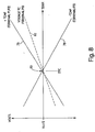
- Figure 8 is a graph showing how the voltages on external terminals P1, P2 and P3 vary with temperature, both with and without resistor R3 being connected between terminal P3 and one of terminals P1 and P2.
- curve 76 represents the voltage on both of external terminals P1 and P2 when resistor R3 is not connected to either of them
- curve 78 represents the voltage on external terminal P3 when resistor R3 is not connected to it
- curve 82 represents the voltage on external terminal P3 when resistor R3 is connected between terminal P3 and one of terminals P1 and P2.
- Curves 76, 78 and 80 are shown as they would appear after bridge resistors TF1 and TF2, or gain-setting resistors TF3-TF5, have been trimmed properly. That is, after selected ones of resistors TF1-TF5 have been trimmed properly, curves 76, 78 and 80 will converge at a point 80, which corresponds to an ambient temperature of 27° Celsius.
- resistor R3 When resistor R3 is connected between terminal P3 and one of terminals P1 and P2, external terminal P3 will form a node of a voltage divider including at least two resistors that divide the voltage between node 88 and the output of operational amplifier 86. Specifically, when resistor R3 is connected between terminal P3 and terminal P1, terminal P3 will form a node of a voltage divider including resistor R2 (which includes resistors DR3 and TF7) and resistor R3, and when resistor R3 is connected between terminal P3 and terminal P2, terminal P3 will form a node of a voltage divider including resistor R1 (which includes resistors DR2 and TF6), resistor R2 (which includes resistors DR3 and TF7), and resistor R3.
- resistor R1 which includes resistors DR2 and TF6
- resistor R2 which includes resistors DR3 and TF7
- the voltage at terminal P3 resulting from the voltage division performed by these resistors is represented by curve 82 in Figure 8.
- the ability to connect resistor R3 to either of two separate terminals is provided to permit temperature compensation of the device for different types of magnets.
- the connection of resistor R3 between terminals P1 and P3 may permit the compensation of a -2000 parts-per-million (ppm) magnet and the connection of resistor R3 between terminals P2 and P3 may permit the compensation of a -200 ppm magnet.
- resistor R3 After resistor R3 is connected between external terminal P3 and one of external terminals P1 and P2, its value may be trimmed to optimize the slope of curve 82 for the particular application. That is, by adjusting the slope of curve 82, the amount that the voltage at external terminal P3 changes in response to temperature changes will be adjusted. Because the voltage at external terminal P3 controls the magnitude of the Hall current I H generated by voltage-to-current converter 42 (shown in Figure 3), optimizing the slope of curve 82 (by trimming resistor R3) will permit compensation of the temperature dependency of the sensitivity S H of Hall-effect element 20 with a high degree of accuracy.
- each of resistors R1 and R2 includes a series combination of a thin film and a temperature-sensitive diffusion resistor. Diffusion resistors are used in resistors R1 and R2 to add curvature to curve 82 to provide correction for the second-order temperature coefficient of the quad-cell Hall-effect element sensitivity S H .
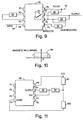
- FIG. 9 is partial block/partial schematic diagram showing a possible embodiment of Hall-effect device 80 and a possible configuration of circuit elements external thereto.
- Hall-effect device 80 is an 8-pin dual-in-line package (DIP) including terminals (i.e., external connectors) P1-P8, several of which are the same terminals shown in previously-described Figures.
- Terminal P8 receives power from high-supply conductor 70 and terminal P4 is connected to an analog ground conductor 84.
- Trimmable resistor R3 is connected between terminals P2 and P3 (or optionally could be connected between terminals P1 and P3).
- Resistors R4-R6 are configured to set the gain of output amplifier 56.
- resistor R4 is connected between terminals P8 and P6 (which is the inverting input of output amplifier 56), resistor R6 is connected between terminals P6 and P5 (which has a voltage equal to VCC/2 on it), and resistor R5 is connected between terminals P6 and P7 (which is the output of amplifier 56).
- Figure 10 is a side-view of an embodiment of Hall-effect device 80 showing how device 80 senses a magnetic field. As shown, the device is configured to sense a magnetic field B oriented transverse to the plane of the device.
- Figure 11 is partial block/partial schematic diagram showing another possible configuration of circuit elements external to device 80, wherein an additional potential divider (including resistors R7 and R10) is connected across the supply to further adjust the offset of the device.
- resistor R7 is connected between terminal P5 and a first terminal of resistor R9 (the second terminal of which is connected to terminal P7)
- resistor R8 is connected between terminal P6 and terminal P7
- resistor R10 is connected between the first terminal of resistor R9 and terminal P3.
- Hall-effect device 80 has been described herein as using, temperature sensitive resistors, any devices capable of producing an output that varies with temperature could equivalently be used without departing from the intended scope of the invention.
- the temperature-variable current source 22 includes a first device that generates a voltage dependent on temperature and a second device that converts the generated voltage into a current to be supplied to Hall-effect element 20, a single device that produces a temperature-dependent current could equivalently be used, or, alternatively, a temperature-dependent voltage source could be used directly as the source of current across terminal pairs of Hall-effect element 20.
- any other external device capable of adjusting the sensitivity of the device equivalently could be employed.
- the semiconductor components have been described herein as being of particular doping types, opposite doping types equivalently may be used.
Landscapes
- Physics & Mathematics (AREA)
- Condensed Matter Physics & Semiconductors (AREA)
- General Physics & Mathematics (AREA)
- Measuring Magnetic Variables (AREA)
- Hall/Mr Elements (AREA)
Claims (25)
- Eine Hall-Effekt Vorrichtung (80) die Folgendes aufweist:dadurch gekennzeichnet, dassein Hall-Effekt Element (20) mit mindestens einem Eingang (34, 36, 38, 40) zum Empfang eines Vorspannsignals und mit mindestens einem Ausgang(34, 36, 38, 40) zum Liefern eines Ausgangssignals, abhängig von dem Vorspannsignal und von einem Magnetfeld, welches das Hall-Effekt Element (20) unterbricht (intercepts);mindestens ein Ausgangsleiter (P7) um ein Ausgangssignal, ansprechend auf das Ausgangssignal des Hall-Effekt Elements (20) und abhängig von einer Gesamtverstärkung der Hall-Effekt Vorrichtung (80) zu liefern; undeine temperaturveränderbare Verstärkungssteuerschaltung (22), gekoppelt an das Hall-Effekt Element (20) zum Einstellen der Empfindlichkeit der Gesamtverstärkung der Hall-Effekt Vorrichtung (80) gegenüber Temperaturänderungen;
die temperaturveränderbare Verstärkungssteuerschaltung (22) ein Paar von Knoten (P2, P3) derart aufweist, dass dann, wenn eine erste Komponente (R3) zwischen dem Paar von Knoten (P2, P3) gekoppelt ist, eine Charakteristik von nur der ersten Komponente (R3) die Empfindlichkeit der Gesamtverstärkung der Hall-Effekt Vorrichtung (80) gegenüber Temperaturänderungen ändert, ohne im Wesentlichen die Gesamtverstärkung der Hall-Effekt Vorrichtung (80) zu ändern, wenn die Hall-Effekt Vorrichtung (80) auf einer Bezugstemperatur gehalten ist, wobei die temperaturveränderbare Verstärkungssteuerschaltung (22) eine temperaturveränderbare Signalquelle (42, 46) aufweist, und zwar gekoppelt an das Hall-Effekt Element, um das Vorspannsignal dafür derart vorzusehen, dass eine Amplitude des Vorspannsignals sich ansprechend auf die Temperaturänderungen ändert. - Hall-Effekt Vorrichtung (80) nach Anspruch 1, wobei die temperaturveränderbare Signalquelle (42, 46) derart konfiguriert ist, dass dann, wenn die erste Komponente (R3) zwischen das Paar von Knoten (P2, P3) gekoppelt ist, das Ändern der Charakteristik von nur der ersten Komponente (R3) eine Größe ändert, die die Amplitude des Vorspannsignals ändert, und zwar ansprechend auf eine gegebene Temperaturänderung ohne im Wesentlichen die Amplitude des Vorspannsignals dann zu ändern, wenn die Hall-Effekt Vorrichtung (80) auf der Bezugstemperatur gehalten wird.
- Hall-Effekt Vorrichtung (80) nach Anspruch 2, wobei die temperaturveränderbare Signalquelle (42, 46) Folgendes aufweist:eine steuerbare Stromquelle (46) mit einem Steuereingang (72), der einen Vorspannstrom als das Vorspannsignal an das Hall-Effekt Element (20) liefert, undein temperaturempfindliches Signal (42), gekoppelt an den Steuereingang (72) der steuerbaren Stromquelle (46), um ein temperaturabhängiges Steuersignal dafür vorzusehen.
- Hall-Effekt Vorrichtung (80) nach Anspruch 3, wobei die steuerbare Stromquelle (46) eine spannungsgesteuerte Stromquelle aufweist oder ist, und wobei ferner die temperaturempfindliche Signalquelle (42) eine temperaturempfindliche Spannungsquelle aufweist.
- Hall-Effekt Vorrichtung (80) nach einem der Ansprüche 1 bis 4, wobei mindestens einer des Paares von Knoten (P2, P3) einen Knoten eines Potentialteilers (R1, R2, R3) bildet, wenn die erste Komponente (R3) dazwischen gekoppelt ist.
- Hall-Effekt Vorrichtung (80) nach einem der Ansprüche 1 bis 5, wobei die erste Komponente (R3) einen Widerstand mit einem einstellbaren Widerstandswert besitzt.
- Hall-Effekt Vorrichtung (80) nach einem der Ansprüche 1 bis 6, wobei ferner Mittel (22) vorgesehen sind zum Kompensieren der Versetzung (offset) des Hall-Effekt Elements (20).
- Hall-Effekt Vorrichtung (80) nach einem der Ansprüche 1 bis 7, wobei Folgendes vorgesehen ist:wobei die Empfindlichkeitskonstante (S) des Hall-Effekt Elements (20) sich mit Temperaturänderungen des Hall-Effekt Element (20) derart ändert, dass dann, wenn die Amplitude des Vorspannsignals (I) und die Stärke des Magnetfeldes (B) konstant gehalten würden, eine Größe des Ausgangssignals sich in einer bestimmten Polaritätsrichtung ändern würde, wenn eine Temperatur des Hall-Effekt Elements (20) erhöht würde; unddas Hall-Effekt Element (20) ist derart konfiguriert, dass das Ausgangssignal desselben ein Produkt einer Stärke des Magnetfeldes (B) repräsentiert, welches das Hall-Effekt Element unterbricht oder durchschneidet,eine Amplitude des Vorspannsignals (I) und eine Empfindlichkeitskonstante (S) des Hall-Effekt Elements (20),
wobei die Temperatur veränderbare Verstärkungssteuerschaltung (22) derart konfiguriert ist, dass dann, wenn die erste Komponente (R3) zwischen das Paar von Knoten (P2, P3) gekoppelt ist, und die Charakteristik der ersten Komponente (R3) einen ersten Wert besitzt, eine Größe, die die gesamte Verstärkung der Hall-Effekt Vorrichtung (80) in der bestimmten Polaritätsrichtung ändert, und zwar ansprechend auf einen gegebenen Temperaturanstieg, größer ist als eine Größe, mit der sich die Gesamtverstärkung der Hall-Effekt Vorrichtung (80) in der bestimmten Polaritätsrichtung ändern würde, ansprechend auf einen gegebenen Temperaturanstieg, wenn die temperaturveränderbare Verstärkungssteuerschaltung (22) nicht die Gesamtverstärkung der Hall-Effekt Vorrichtung (80), ansprechend auf die Änderung der Temperaturbedingungen ändern würde. - Hall-Effekt Vorrichtung (80) nach Anspruch 8, wobei die temperaturveränderbare Verstärkungssteuerschaltung (22) derart konfiguriert ist, dass dann, wenn die erste Komponente (R3) zwischen das Paar von Knoten (P2, P3) gekoppelt ist und die Charakteristik der ersten Komponente (R3) einen zweiten Wert besitzt, die Größe die die Gesamtverstärkung der Hall-Effekt Vorrichtung (80) ändert und zwar in der speziellen Polaritätsrichtung, ansprechend auf den gegebenen Temperaturanstieg kleiner ist als die Größe mit der sich die Gesamtverstärkung der Hall-Effekt Vorrichtung (80) ändern würde in der speziellen Polaritätsrichtung, ansprechend auf den gegebenen Temperaturanstieg, wenn die temperaturveränderbare Verstärkungssteuerschaltung (22) nicht die Gesamtverstärkung der Hall-Effekt Vorrichtung (80) ändern würde, und zwar ansprechend auf die Änderung der Temperaturbedingungen.
- Hall-Effekt Vorrichtung (80) nach einem der Ansprüche 1 bis 9, wobei Folgendes vorgesehen ist:das Hall-Effekt Element (20) ist in einer integrierten Schaltungspackung angebracht; unddas Paar von Knoten (P2, P3) weist ein Paar von Anschlüssen auf, die sich von der integrierten Schaltungspackung derart erstrecken, dass die erste Komponente (R3) zwischen das Paar von Anschlüssen an einer Stelle außerhalb der Packung gekoppelt werden können.
- Hall-Effekt Vorrichtung (80) nach einem der Ansprüche 1 bis 10, wobei ferner mindestens eine zweite Komponente (TF1, TF2) vorgesehen ist, und zwar gekoppelt an die temperaturveränderbare Verstärkungssteuerschaltung (22), wobei eine Charakteristik von der mindestens einen zweiten Komponente (TF1, TF2) einstellbar ist, um die Bezugstemperatur auszuwählen, bei der die Änderung der Charakteristik von nur der ersten Komponente (R3) nicht im Wesentlichen die Gesamtverstärkung der Hall-Effekt Vorrichtung ändert.
- Hall-Effekt Vorrichtung (80) nach Anspruch 2, wobei die temperaturveränderbare Signalquelle (42, 46) derart konfiguriert ist, dass dann, wenn die erste Komponente (R3)zwischen das Paar von Knoten (P2, P3) gekoppelt ist und die Charakteristik der ersten Komponente (R3) einen ersten Wert besitzt, eine Amplitude des Vorspannsignals dann ansteigt, wenn die Temperatur ansteigt, und wobei dann, wenn die erste Komponente (R3) zwischen das Paar von Knoten (P2, P3) gekoppelt ist und die Charakteristik der ersten Komponente (R3) einen zweiten Wert besitzt, das Vorspannsignal abnimmt, wenn die Temperatur ansteigt.
- Hall-Effekt Vorrichtung (80) nach Anspruch 2, wobei die temperaturveränderbare Signalquelle (42, 46) eine Stromquelle (46) aufweist, die einen Vorspannstrom als das Vorspannsignal für das Hall-Effekt Element (20) vorsieht.
- Hall-Effekt Vorrichtung (80) nach Anspruch 5, wobei:wobei der zweite Knoten die invertierte temperaturabhängige Spannung daran anliegend aufweist.die temperaturveränderbare Verstärkungssteuerschaltung (22) einen invertierenden Verstärker (86) aufweist, der die nicht invertierte temperaturabhängige Spannung invertiert, um eine invertierte temperaturabhängige Spannung zu erzeugen; undder Potentialteiler (R1, R2, R3) zwischen einen ersten Knoten (88) und einen zweiten Knoten gekoppelt ist, wobei der erste Knoten daran anliegend die nicht invertierte temperaturabhängige Spannung aufweist, und
- Hall-Effekt Vorrichtung (80) nach einem der Ansprüche 1 bis 14, und zwar in Kombination mit der ersten Komponente (R3).
- Hall-Effekt Vorrichtung (80) nach einem der Ansprüche 1 bis 15, wobei die temperaturveränderbare Verstärkungssteuerschaltung (22) eine temperaturabhängige Spannungsquelle (74), eine spannungsgesteuerte Verstärkungseinstellschaltung (46) und einen Spannungsteiler (R1, R2, R3) aufweist, und zwar mit mindestens einem Knoten (88), gekoppelt an die Spannungsquelle (74), und zwar zum Empfang einer temperaturabhängigen Spannung davon, und ferner mit einem zweiten Knoten (72), gekoppelt mit der Verstärkungseinstellschaltung (46) um eine Steuerspannung daran zu liefern, wobei der Spannungsteil (R1, R2, R3) die erste Komponente (R3) aufweist, und derart konfiguriert ist, dass die Einstellung der Charakteristik von nur der ersten Komponente (R3) ein Verhältnis der Komponentenwerte im Spannungsteil (R1, R2, R3) derart ändert, dass die Spannung an dem zweiten Knoten (72) geändert wird.
- Verfahren zum Kompensieren der Effekt von Temperaturveränderungen an einem Hall-Effekt Element (20), wobei die folgenden Schritte vorgesehen sind:(a) Vorsehen einer Hall-Effekt Vorrichtung (80) einschließlich eines Hall-Effekt Elements (20) und einer temperaturveränderbaren Verstärkungssteuerschaltung (22), gekoppelt an das Hall-Effekt Element (20), um die Empfindlichkeit der Verstärkung der Hall-Effekt Vorrichtung (80) gegenüber Temperaturänderungen einzustellen, dadurch gekennzeichnet, dass das Verfahren ferner Folgendes aufweist:(b) Koppeln einer ersten Komponente (R3) zwischen ein Paar von Knoten (P2, P3) der temperaturveränderbaren Verstärkungssteuerschaltung (22), um die Empfindlichkeit der Verstärkung der Hall-Effekt Vorrichtung (80) auf die Temperaturveränderungen einzustellen; und(c) Ändern einer Charakteristik von nur der ersten Komponente (R3) zur Einstellung der Empfindlichkeit der Verstärkung der Hall-Effekt Vorrichtung (80) auf Temperaturveränderungen, ohne im Wesentlichen die Verstärkung der Hall-Effekt Vorrichtung (80) zu ändern, wenn die Hall-Effekt Vorrichtung (80) auf einer Bezugstemperatur gehalten ist.
- Verfahren nach Anspruch 17, wobei Folgendes vorgesehen ist:der Schritt (a) weist einen Schritt auf zum Vorsehen einer temperaturveränderbaren Signalquelle (42, 46) als der temperaturveränderbaren Verstärkungssteuerschaltung (22), wobei die temperaturveränderbare Signalquelle (42, 46) mit dem Hall-Effekt Element (20) gekoppelt ist, um ein Vorspannsignal für mindestens einen Eingang (34, 36, 38, 40) des Hall-Effekt Elements derart vorzusehen, dass eine Amplitude des Vorspannsignals sich ansprechend auf die Temperaturänderungen ändert; undder Schritt (b) weist einen Schritt (b1) auf und war zum Koppeln der ersten Komponente (R3) zwischen das Paar von Knoten (P2, P3), um eine Empfindlichkeit der temperaturveränderbaren Signalquelle (42, 46) auf Temperaturveränderungen einzustellen; undder Schritt (c) weist einen Schritt des Ändern der Charakteristik von nur der ersten Komponente (R3) auf, um eine Größe einzustellen, die die Größe der Amplitude des Vorspannsignals ändert, und zwar ansprechend auf eine gegebene Temperaturänderung, ohne im Wesentlichen die Amplitude des Vorspannsignals dann zu ändern, wenn die Hall-Effekt Vorrichtung (80) auf der Bezugstemperatur gehalten wird.
- Verfahren nach Anspruch 17 oder 18, wobei die Hall-Effekt Vorrichtung (80) in einer integrierten Schaltung enthalten ist, und wobei der Schritt (b) einen Schritt des Koppelns der ersten Komponente (R3) zwischen einem Paar von externen Anschlüssen (P2, P3) der integrierten Schaltung aufweist, um die Empfindlichkeit der Verstärkung der Hall-Effekt Vorrichtung (80) gegenüber Temperaturänderungen einzustellen.
- Verfahren nach einem der Ansprüche 17 bis 19, wobei ferner ein Schritt des Einstellens der Bezugstemperatur vorgesehen ist.
- Hall-Effekt Vorrichtung (80) nach Anspruch 8 bis 10, wobei die temperaturveränderbare Signalquelle (42, 46) Folgendes aufweist:eine steuerbare Stromquelle (46) mit einem Steuereingang (72), der ein Vorspannstrom als das Vorspannsignal an das Hall-Effekt Element (20) liefert, undeine temperaturempfindliche Signalquelle (42), gekoppelt mit der Stromquelle (46), um ein temperaturabhängiges Steuersignal für den Steuereingang (72) der steuerbaren Stromquelle (46) zu liefern, wobei die temperaturempfindliche Signalquelle (42) derart konfiguriert ist, dass dann, wenn die erste Komponente (R3) zwischen das Paar von Knoten (P2, P3) gekoppelt ist, eine Amplitude des temperaturabhängigen Steuersignals veranlasst wird sich zu ändern, wenn die Temperatur der Hall-Effekt Vorrichtung (80) ändert, wodurch bewirkt wird, dass die Amplitude des Vorspannstromes sich ändert, wenn die Temperatur der Hall-Effekt Vorrichtung (80) sich ändert.
- Hall-Effekt Vorrichtung (80) nach Anspruch 21, wobei die steuerbare Stromquelle (46) eine spannungsgesteuerte Stromquelle aufweist, und wobei die temperaturempfindliche Signalquelle (42) eine temperaturempfindliche Spannungsquelle aufweist.
- Hall-Effekt Vorrichtung (80) nach Anspruch 21, wobei Folgendes vorgesehen ist:die temperaturveränderbare Signalquelle (22) weist eine Stromquelle (46) auf, die einen Vorspannstrom als das Vorspannsignal (I) für das Hall-Effekt Element (20) vorsieht; unddie temperaturveränderbare Signalquelle (42) ist derart konfiguriert, dass dann, wenn die erste Komponente (R3) zwischen das Paar von Knoten (P2, P3) gekoppelt ist, eine Amplitude des Vorspannstromes veranlasst wird sich zu ändern, wenn die Temperatur sich ändert.
- Hall-Effekt Vorrichtung (80) nach einem der Ansprüche 21 bis 23, wobei Folgendes vorgesehen ist:die temperaturveränderbare Verstärkungssteuerschaltung (22) weist einen invertierten Verstärker (86) auf, der eine nicht invertierte temperaturabhängige Spannung invertiert, um eine invertierte temperaturabhängige Spannung zu erzeugen;die erste Komponente (R3) weist einen Widerstand auf; unddie temperaturveränderbare Verstärkungssteuerschaltung (22) ist derart konfiguriert, dass dann, wenn der Widerstand (R3) zwischen das Paar von Knoten (P2, P3) gekoppelt ist, der Widerstand (R3) in einem Spannungsteiler (R1, R2, R3) eingeschlossen ist, und zwar gekoppelt zwischen einen ersten Knoten (88) mit der nicht invertierten temperaturabhängigen Spannung daran anliegend, und einen zweiten Knoten mit der invertierten temperaturabhängigen Spannung daran anliegend, wobei die Empfindlichkeit der Gesamtverstärkung der Hall-Effekt Vorrichtung (80) ansprechend auf eine Spannung am Knoten (72) des Spannungsteiles eingestellt wird.
- Hall-Effekt Vorrichtung (80) nach einem der Ansprüche 21 bis 24, wobei die temperaturveränderbare Verstärkungssteuerschaltung (22) eine temperaturabhängige Spannungsquelle (74), eine spannungsgesteuerte Verstärkungseinstellschaltung (46) und einen Spannungsteiler (R1, R2, R3) mit mindestens einen ersten Knoten (88), gekoppelt an die Spannungsquelle (74) zum Empfang einer temperaturabhängigen Spannung davon, und ferner einen zweiten Knoten (72) aufweist, und zwar gekoppelt mit der Verstärkungseinstellschaltung (46) um eine Steuerspannung daran vorzusehen, wobei der Spannungsteiler (R1, R2, R3) eine erste Komponente (R3) aufweist und derart konfiguriert ist, dass die Einstellung der Charakteristik von nur einer Komponente (R3) ein Verhältnis der Komponentenwerte in dem Spannungsteiler (R1, R2, R3) derart ändert, dass die Spannung am zweiten Knoten (72) geändert wird.
Applications Claiming Priority (3)
| Application Number | Priority Date | Filing Date | Title |
|---|---|---|---|
| US953884 | 1997-10-20 | ||
| US08/953,884 US6154027A (en) | 1997-10-20 | 1997-10-20 | Monolithic magnetic sensor having externally adjustable temperature compensation |
| PCT/US1998/016931 WO1999021023A1 (en) | 1997-10-20 | 1998-08-14 | Monolithic magnetic sensor having externally adjustable temperature compensation |
Publications (2)
| Publication Number | Publication Date |
|---|---|
| EP1025448A1 EP1025448A1 (de) | 2000-08-09 |
| EP1025448B1 true EP1025448B1 (de) | 2005-10-19 |
Family
ID=25494663
Family Applications (1)
| Application Number | Title | Priority Date | Filing Date |
|---|---|---|---|
| EP98939956A Expired - Lifetime EP1025448B1 (de) | 1997-10-20 | 1998-08-14 | Monolithischer magnetischer sensor mit extern einstellbarer temperaturkompensation |
Country Status (5)
| Country | Link |
|---|---|
| US (1) | US6154027A (de) |
| EP (1) | EP1025448B1 (de) |
| JP (1) | JP2001521152A (de) |
| DE (1) | DE69831967T2 (de) |
| WO (1) | WO1999021023A1 (de) |
Families Citing this family (48)
| Publication number | Priority date | Publication date | Assignee | Title |
|---|---|---|---|---|
| DE19910411C2 (de) * | 1999-03-10 | 2001-08-30 | Daimler Chrysler Ag | Verfahren und Vorrichtung zur Offset-kompensierten Magnetfeldmessung mittels eines Hallsensors |
| DE19943128A1 (de) * | 1999-09-09 | 2001-04-12 | Fraunhofer Ges Forschung | Hall-Sensoranordnung zur Offset-kompensierten Magnetfeldmessung |
| DE19951045B4 (de) * | 1999-10-22 | 2005-03-17 | Micronas Gmbh | Magnetfeldsensor mit Kettenleiterfilter |
| US6777932B2 (en) | 2000-03-23 | 2004-08-17 | Matsushita Electric Industrial Co., Ltd. | Magnetic field sensor |
| JP3315397B2 (ja) | 2000-03-23 | 2002-08-19 | 松下電器産業株式会社 | 磁界センサおよび磁界検出方法 |
| US6357279B1 (en) * | 2001-01-29 | 2002-03-19 | Leco Corporation | Control circuit for thermal conductivity cell |
| DE10117382B4 (de) * | 2001-04-06 | 2006-04-06 | Infineon Technologies Ag | Schaltungsanordnung und Sensorvorrichtung |
| JP4451577B2 (ja) * | 2001-07-26 | 2010-04-14 | パナソニック株式会社 | 磁界センサ |
| US6794863B2 (en) * | 2002-11-13 | 2004-09-21 | Matsushta Electric Industrial Co., Ltd. | Magnetic field sensor, method for detecting magnetic field and device for detecting magnetic field |
| DE10313642A1 (de) * | 2003-03-26 | 2004-10-14 | Micronas Gmbh | Offset-reduzierter Hall-sensor |
| NL1024114C1 (nl) * | 2003-08-15 | 2005-02-16 | Systematic Design Holding B V | Werkwijze en inrichting voor het verrichten van metingen aan magnetische velden met gebruik van een hall-sensor. |
| NL1025089C2 (nl) * | 2003-12-19 | 2005-06-21 | Xensor Integration B V | Magneetveldsensor, drager van een dergelijke magneetveldsensor en een kompas, voorzien van een dergelijke magneetveldsensor. |
| JP4514104B2 (ja) * | 2004-03-30 | 2010-07-28 | 旭化成エレクトロニクス株式会社 | 磁気検出装置 |
| JP4049125B2 (ja) * | 2004-05-20 | 2008-02-20 | コニカミノルタオプト株式会社 | 位置検出装置、手振れ補正機構、および撮像装置 |
| JP4641775B2 (ja) * | 2004-09-29 | 2011-03-02 | ルネサスエレクトロニクス株式会社 | 磁気検出用半導体集積回路およびそれを搭載した電子部品 |
| EP1830162B1 (de) * | 2004-12-14 | 2015-04-01 | NTN Corporation | Rotationsdetektionsvorrichtung und damit ausgestattetes lager |
| JP4553714B2 (ja) * | 2004-12-14 | 2010-09-29 | Ntn株式会社 | 回転検出装置および回転検出装置付き軸受 |
| US7180359B2 (en) * | 2004-12-22 | 2007-02-20 | Analog Devices, Inc. | Logarithmic temperature compensation for detectors |
| DE102005028461A1 (de) * | 2005-06-17 | 2006-12-28 | Micronas Gmbh | Verfahren zum Testen eines Wafers, insbesondere Hall-Magnetfeld-Sensors und Wafer bzw. Hallsensor |
| JP2008309626A (ja) * | 2007-06-14 | 2008-12-25 | Oki Electric Ind Co Ltd | 感磁出力ic |
| GB0723973D0 (en) * | 2007-12-07 | 2008-01-16 | Melexis Nv | Hall sensor array |
| US8054071B2 (en) * | 2008-03-06 | 2011-11-08 | Allegro Microsystems, Inc. | Two-terminal linear sensor |
| FR2947060B1 (fr) * | 2009-06-18 | 2011-10-28 | Socomec Sa | Capteur de champ magnetique a effet hall |
| EP2450719A4 (de) * | 2009-06-30 | 2017-12-06 | Asahi Kasei Microdevices Corporation | Magnetischer sensor |
| US9013167B2 (en) * | 2010-11-09 | 2015-04-21 | Texas Instruments Incorporated | Hall effect device having voltage based biasing for temperature compensation |
| US8957676B2 (en) * | 2011-05-06 | 2015-02-17 | Allegro Microsystems, Llc | Magnetic field sensor having a control node to receive a control signal to adjust a threshold |
| DE102011077580A1 (de) | 2011-06-16 | 2012-12-20 | Robert Bosch Gmbh | Hallsensor und Verfahren zum Betreiben eines Hallsensors |
| JP5385490B1 (ja) | 2012-01-25 | 2014-01-08 | 旭化成エレクトロニクス株式会社 | ホール起電力信号検出回路及びその電流センサ |
| JP5865108B2 (ja) * | 2012-02-16 | 2016-02-17 | セイコーインスツル株式会社 | 磁気センサ装置 |
| US9817083B2 (en) * | 2012-07-05 | 2017-11-14 | Allegro Microsystems, Llc | Magnetic field sensors and associated methods for removing undesirable spectral components |
| US9063174B2 (en) * | 2012-11-14 | 2015-06-23 | Olympus Scientific Solutions Americas Inc. | Hall effect measurement instrument with temperature compensation |
| JP6158682B2 (ja) * | 2013-10-25 | 2017-07-05 | エスアイアイ・セミコンダクタ株式会社 | 磁気センサ回路 |
| US9297865B2 (en) * | 2013-11-12 | 2016-03-29 | Olympus Scientific Solutions Americas Inc. | Hall effect measurement instrument with temperature compensation |
| JP6457192B2 (ja) * | 2014-03-31 | 2019-01-23 | 旭化成エレクトロニクス株式会社 | ホール起電力信号処理装置、電流センサ及びホール起電力信号処理方法 |
| CN103929166B (zh) * | 2014-04-25 | 2016-11-16 | 成都芯进电子有限公司 | 一种可编程开关型霍尔传感器 |
| DE102015117109B4 (de) * | 2015-10-07 | 2025-07-10 | Infineon Technologies Ag | Digital gesteuerte Ausgangsamplitude eines Analogsensorsignals |
| US10101410B2 (en) | 2015-10-21 | 2018-10-16 | Allegro Microsystems, Llc | Methods and apparatus for sensor having fault trip level setting |
| JP2017161475A (ja) * | 2016-03-11 | 2017-09-14 | 株式会社東芝 | 半導体装置および磁気センサ |
| JP6568825B2 (ja) * | 2016-06-20 | 2019-08-28 | 旭化成エレクトロニクス株式会社 | 制御回路および電流センサ |
| CN107014401B (zh) * | 2016-11-18 | 2019-12-31 | 清华四川能源互联网研究院 | 一种磁阻传感器温度补偿装置 |
| US10444299B2 (en) | 2017-09-11 | 2019-10-15 | Allegro Microsystems, Llc | Magnetic field sensor's front end and associated mixed signal method for removing chopper's related ripple |
| US10481219B2 (en) | 2017-09-11 | 2019-11-19 | Allegro Microsystems, Llc | Magnetic field sensor with feedback loop for test signal processing |
| US10574259B2 (en) * | 2017-10-03 | 2020-02-25 | Invensense, Inc. | Continuous-time sensing apparatus |
| US11047933B2 (en) | 2019-04-02 | 2021-06-29 | Allegro Microsystems, Llc | Fast response magnetic field sensors and associated methods for removing undesirable spectral components |
| JP7367350B2 (ja) * | 2019-06-21 | 2023-10-24 | セイコーエプソン株式会社 | 回路装置、発振器、電子機器及び移動体 |
| US12153101B2 (en) | 2022-01-27 | 2024-11-26 | Nxp Usa, Inc. | Sensor calibration circuit |
| DE102022129671B3 (de) * | 2022-11-09 | 2024-03-07 | Senis Ag | Magnetfeldsensorsystem mit einem temperaturgangskompensierten Ausgangssignal sowie Verfahren für die Temperaturgangskompensation eines Ausgangssignals eines Magnetfeldsensorsystems |
| CN117519404B (zh) * | 2024-01-05 | 2024-03-22 | 深圳市信瑞达电力设备有限公司 | 一种调节霍尔元件输出增益的方法和电路拓扑 |
Family Cites Families (14)
| Publication number | Priority date | Publication date | Assignee | Title |
|---|---|---|---|---|
| US4804957A (en) * | 1985-11-27 | 1989-02-14 | Triad Communications, Inc. | Utility meter and submetering system |
| US4734594A (en) * | 1986-12-31 | 1988-03-29 | Honeywell Inc. | Offset correction for sensor with temperature dependent sensitivity |
| US4760285A (en) * | 1987-03-30 | 1988-07-26 | Honeywell Inc. | Hall effect device with epitaxal layer resistive means for providing temperature independent sensitivity |
| DE3827606A1 (de) * | 1987-08-18 | 1989-03-02 | Kostal Leopold Gmbh & Co Kg | Temperaturkompensationsschaltung fuer einen hall-generator |
| US5317259A (en) * | 1990-05-14 | 1994-05-31 | The United States Of America As Represented By The United States Department Of Energy | DC-based magnetic field controller |
| JP2750788B2 (ja) * | 1991-08-08 | 1998-05-13 | ローム株式会社 | モータ制御回路およびモータ制御装置 |
| EP0548391B1 (de) * | 1991-12-21 | 1997-07-23 | Deutsche ITT Industries GmbH | Offsetkompensierter Hallsensor |
| US5389889A (en) * | 1993-09-10 | 1995-02-14 | Allegro Microsystems, Inc. | Temperature-compensated current source for use in a hall analog magnetic-field detector |
| DE4431703C2 (de) * | 1994-09-06 | 1997-01-30 | Itt Ind Gmbh Deutsche | Magnetfeldsensor mit Hallelement |
| US5900995A (en) * | 1994-11-25 | 1999-05-04 | Canon Kabushiki Kaisha | Driving device and optical apparatus |
| US5589792A (en) * | 1995-04-19 | 1996-12-31 | Analog Devices, Inc. | Resistor programmable temperature switch |
| DE19544863C2 (de) * | 1995-12-01 | 2000-01-13 | Bosch Gmbh Robert | Sensorvorrichtung |
| US5621319A (en) * | 1995-12-08 | 1997-04-15 | Allegro Microsystems, Inc. | Chopped hall sensor with synchronously chopped sample-and-hold circuit |
| US5686827A (en) * | 1996-02-09 | 1997-11-11 | Eaton Corporation | Temperature compensated Hall effect device |
-
1997
- 1997-10-20 US US08/953,884 patent/US6154027A/en not_active Expired - Lifetime
-
1998
- 1998-08-14 JP JP2000517288A patent/JP2001521152A/ja active Pending
- 1998-08-14 DE DE69831967T patent/DE69831967T2/de not_active Expired - Lifetime
- 1998-08-14 EP EP98939956A patent/EP1025448B1/de not_active Expired - Lifetime
- 1998-08-14 WO PCT/US1998/016931 patent/WO1999021023A1/en not_active Ceased
Also Published As
| Publication number | Publication date |
|---|---|
| DE69831967D1 (de) | 2005-11-24 |
| WO1999021023A1 (en) | 1999-04-29 |
| EP1025448A1 (de) | 2000-08-09 |
| US6154027A (en) | 2000-11-28 |
| DE69831967T2 (de) | 2006-07-27 |
| JP2001521152A (ja) | 2001-11-06 |
Similar Documents
| Publication | Publication Date | Title |
|---|---|---|
| US6154027A (en) | Monolithic magnetic sensor having externally adjustable temperature compensation | |
| US7345476B2 (en) | Method and apparatus for measuring an entity of a magnetic field by using a hall plate, an excitation signal and a detection signal | |
| Bilotti et al. | Monolithic magnetic Hall sensor using dynamic quadrature offset cancellation | |
| EP0859964B1 (de) | Verfahren zum reduzieren der offsetpannung einer hallanordnung | |
| US4727323A (en) | Magneto-resistive differential sensor system | |
| US7605580B2 (en) | Integrated hybrid current sensor | |
| EP1143536B1 (de) | Halbleiterbauelement | |
| US5621320A (en) | Magnetoresistance type sensor device for detecting change of magnetic field | |
| EP3206037B1 (de) | Verfahren und vorrichtung zur messung des elektrischen stromes mittels einer selbstausgleichenden konfiguration von magnetfeldsensoren | |
| US4875011A (en) | Magnetic sensor using integrated silicon Hall effect elements formed on the (100) plane of a silicon substrate | |
| CN210400415U (zh) | 霍尔传感器 | |
| EP3422032B1 (de) | Eine temperaturkompensationsschaltung, entsprechende vorrichtung und verfahren | |
| EP0052981B1 (de) | Schaltung zur Elimination der In-Phasen-Spannung bei einem Hall-Element | |
| US6392400B1 (en) | High linearity, low offset interface for Hall effect devices | |
| US4683429A (en) | Electrical circuit which is linearly responsive to changes in magnetic field intensity | |
| Schott et al. | High-accuracy analog Hall probe | |
| Munter | Electronic circuitry for a smart spinning-current Hall plate with low offset | |
| Rekalova et al. | Magnetic induction transducers based on silicon planar transistors | |
| US4710652A (en) | Interference signal component compensation circuit | |
| US11408945B2 (en) | Magnetic field sensor with stacked transducers and capacitive summing amplifier | |
| Kammerer et al. | Hall effect sensors integrated in standard technology and optimized with on-chip circuitry | |
| JPS5819149B2 (ja) | ホ−ル効果装置 | |
| JPH05326986A (ja) | センサ出力安定化回路 | |
| MXPA01002653A (es) | Interface de bajo deplazamiento, alta linearidad para dispositivos de efecto hall | |
| JPS58178272A (ja) | 磁気センサ− |
Legal Events
| Date | Code | Title | Description |
|---|---|---|---|
| PUAI | Public reference made under article 153(3) epc to a published international application that has entered the european phase |
Free format text: ORIGINAL CODE: 0009012 |
|
| 17P | Request for examination filed |
Effective date: 20000510 |
|
| AK | Designated contracting states |
Kind code of ref document: A1 Designated state(s): DE FR GB |
|
| 17Q | First examination report despatched |
Effective date: 20010117 |
|
| GRAP | Despatch of communication of intention to grant a patent |
Free format text: ORIGINAL CODE: EPIDOSNIGR1 |
|
| GRAS | Grant fee paid |
Free format text: ORIGINAL CODE: EPIDOSNIGR3 |
|
| GRAA | (expected) grant |
Free format text: ORIGINAL CODE: 0009210 |
|
| AK | Designated contracting states |
Kind code of ref document: B1 Designated state(s): DE FR GB |
|
| REG | Reference to a national code |
Ref country code: GB Ref legal event code: FG4D |
|
| REF | Corresponds to: |
Ref document number: 69831967 Country of ref document: DE Date of ref document: 20051124 Kind code of ref document: P |
|
| ET | Fr: translation filed | ||
| PLBE | No opposition filed within time limit |
Free format text: ORIGINAL CODE: 0009261 |
|
| STAA | Information on the status of an ep patent application or granted ep patent |
Free format text: STATUS: NO OPPOSITION FILED WITHIN TIME LIMIT |
|
| 26N | No opposition filed |
Effective date: 20060720 |
|
| GBPC | Gb: european patent ceased through non-payment of renewal fee |
Effective date: 20060814 |
|
| PG25 | Lapsed in a contracting state [announced via postgrant information from national office to epo] |
Ref country code: GB Free format text: LAPSE BECAUSE OF NON-PAYMENT OF DUE FEES Effective date: 20060814 |
|
| REG | Reference to a national code |
Ref country code: FR Ref legal event code: PLFP Year of fee payment: 19 |
|
| PGFP | Annual fee paid to national office [announced via postgrant information from national office to epo] |
Ref country code: DE Payment date: 20160809 Year of fee payment: 19 |
|
| PGFP | Annual fee paid to national office [announced via postgrant information from national office to epo] |
Ref country code: FR Payment date: 20160712 Year of fee payment: 19 |
|
| REG | Reference to a national code |
Ref country code: DE Ref legal event code: R119 Ref document number: 69831967 Country of ref document: DE |
|
| REG | Reference to a national code |
Ref country code: FR Ref legal event code: ST Effective date: 20180430 |
|
| PG25 | Lapsed in a contracting state [announced via postgrant information from national office to epo] |
Ref country code: DE Free format text: LAPSE BECAUSE OF NON-PAYMENT OF DUE FEES Effective date: 20180301 |
|
| PG25 | Lapsed in a contracting state [announced via postgrant information from national office to epo] |
Ref country code: FR Free format text: LAPSE BECAUSE OF NON-PAYMENT OF DUE FEES Effective date: 20170831 |