EP1009046B1 - Rangée d'éléments à électroluminescence, procédé de fabrication de la rangée et appareil de formation d'images - Google Patents
Rangée d'éléments à électroluminescence, procédé de fabrication de la rangée et appareil de formation d'images Download PDFInfo
- Publication number
- EP1009046B1 EP1009046B1 EP99308289A EP99308289A EP1009046B1 EP 1009046 B1 EP1009046 B1 EP 1009046B1 EP 99308289 A EP99308289 A EP 99308289A EP 99308289 A EP99308289 A EP 99308289A EP 1009046 B1 EP1009046 B1 EP 1009046B1
- Authority
- EP
- European Patent Office
- Prior art keywords
- light emitting
- light
- emitting element
- electrodes
- element array
- Prior art date
- Legal status (The legal status is an assumption and is not a legal conclusion. Google has not performed a legal analysis and makes no representation as to the accuracy of the status listed.)
- Expired - Lifetime
Links
Images


Classifications
-
- H—ELECTRICITY
- H10—SEMICONDUCTOR DEVICES; ELECTRIC SOLID-STATE DEVICES NOT OTHERWISE PROVIDED FOR
- H10K—ORGANIC ELECTRIC SOLID-STATE DEVICES
- H10K71/00—Manufacture or treatment specially adapted for the organic devices covered by this subclass
- H10K71/70—Testing, e.g. accelerated lifetime tests
-
- B—PERFORMING OPERATIONS; TRANSPORTING
- B41—PRINTING; LINING MACHINES; TYPEWRITERS; STAMPS
- B41J—TYPEWRITERS; SELECTIVE PRINTING MECHANISMS, i.e. MECHANISMS PRINTING OTHERWISE THAN FROM A FORME; CORRECTION OF TYPOGRAPHICAL ERRORS
- B41J2/00—Typewriters or selective printing mechanisms characterised by the printing or marking process for which they are designed
- B41J2/435—Typewriters or selective printing mechanisms characterised by the printing or marking process for which they are designed characterised by selective application of radiation to a printing material or impression-transfer material
- B41J2/447—Typewriters or selective printing mechanisms characterised by the printing or marking process for which they are designed characterised by selective application of radiation to a printing material or impression-transfer material using arrays of radiation sources
- B41J2/45—Typewriters or selective printing mechanisms characterised by the printing or marking process for which they are designed characterised by selective application of radiation to a printing material or impression-transfer material using arrays of radiation sources using light-emitting diode [LED] or laser arrays
-
- H—ELECTRICITY
- H10—SEMICONDUCTOR DEVICES; ELECTRIC SOLID-STATE DEVICES NOT OTHERWISE PROVIDED FOR
- H10K—ORGANIC ELECTRIC SOLID-STATE DEVICES
- H10K59/00—Integrated devices, or assemblies of multiple devices, comprising at least one organic light-emitting element covered by group H10K50/00
- H10K59/10—OLED displays
- H10K59/17—Passive-matrix OLED displays
-
- H—ELECTRICITY
- H10—SEMICONDUCTOR DEVICES; ELECTRIC SOLID-STATE DEVICES NOT OTHERWISE PROVIDED FOR
- H10K—ORGANIC ELECTRIC SOLID-STATE DEVICES
- H10K71/00—Manufacture or treatment specially adapted for the organic devices covered by this subclass
- H10K71/20—Changing the shape of the active layer in the devices, e.g. patterning
- H10K71/211—Changing the shape of the active layer in the devices, e.g. patterning by selective transformation of an existing layer
-
- H—ELECTRICITY
- H10—SEMICONDUCTOR DEVICES; ELECTRIC SOLID-STATE DEVICES NOT OTHERWISE PROVIDED FOR
- H10K—ORGANIC ELECTRIC SOLID-STATE DEVICES
- H10K2102/00—Constructional details relating to the organic devices covered by this subclass
- H10K2102/10—Transparent electrodes, e.g. using graphene
- H10K2102/101—Transparent electrodes, e.g. using graphene comprising transparent conductive oxides [TCO]
- H10K2102/103—Transparent electrodes, e.g. using graphene comprising transparent conductive oxides [TCO] comprising indium oxides, e.g. ITO
-
- H—ELECTRICITY
- H10—SEMICONDUCTOR DEVICES; ELECTRIC SOLID-STATE DEVICES NOT OTHERWISE PROVIDED FOR
- H10K—ORGANIC ELECTRIC SOLID-STATE DEVICES
- H10K71/00—Manufacture or treatment specially adapted for the organic devices covered by this subclass
- H10K71/40—Thermal treatment, e.g. annealing in the presence of a solvent vapour
- H10K71/421—Thermal treatment, e.g. annealing in the presence of a solvent vapour using coherent electromagnetic radiation, e.g. laser annealing
-
- H—ELECTRICITY
- H10—SEMICONDUCTOR DEVICES; ELECTRIC SOLID-STATE DEVICES NOT OTHERWISE PROVIDED FOR
- H10K—ORGANIC ELECTRIC SOLID-STATE DEVICES
- H10K85/00—Organic materials used in the body or electrodes of devices covered by this subclass
- H10K85/30—Coordination compounds
- H10K85/321—Metal complexes comprising a group IIIA element, e.g. Tris (8-hydroxyquinoline) gallium [Gaq3]
- H10K85/324—Metal complexes comprising a group IIIA element, e.g. Tris (8-hydroxyquinoline) gallium [Gaq3] comprising aluminium, e.g. Alq3
-
- Y—GENERAL TAGGING OF NEW TECHNOLOGICAL DEVELOPMENTS; GENERAL TAGGING OF CROSS-SECTIONAL TECHNOLOGIES SPANNING OVER SEVERAL SECTIONS OF THE IPC; TECHNICAL SUBJECTS COVERED BY FORMER USPC CROSS-REFERENCE ART COLLECTIONS [XRACs] AND DIGESTS
- Y10—TECHNICAL SUBJECTS COVERED BY FORMER USPC
- Y10S—TECHNICAL SUBJECTS COVERED BY FORMER USPC CROSS-REFERENCE ART COLLECTIONS [XRACs] AND DIGESTS
- Y10S257/00—Active solid-state devices, e.g. transistors, solid-state diodes
- Y10S257/918—Light emitting regenerative switching device, e.g. light emitting scr arrays, circuitry
Definitions
- the present invention relates to a light emitting element array, an image forming apparatus including an electrophotographic photosensitive member using the light emitting element array for forming an image through the exposure of the photosensitive member, and a method of producing the light emitting element array.
- Light emitting element arrays of the kind considered herein comprise a plurality of light emitting elements each having a pair of electrodes and a light emitting layer disposed between the pair of electrodes, wherein the light emissive areas of the respective light emitting elements are limited by the areas of overlap of the respective pairs of electrodes and the direction of light emission is transverse to the plane of the light emitting layer of each light emitting element.
- An example of such an array having an organic light emitting layer is described in United States Patent US-A-5482896.
- the formation of an image by electrophotography is a process consisting of a series of the following steps as is already known: forming a latent image by forming an optical image on a photosensitive member with a light emitting device, developing the latent image with a toner, transferring the image to a transfer material (paper), fixing it and finally cleaning the photosensitive member.
- a laser optical system in which a laser beam scanning is performed through a polygon mirror is widely used as an exposure unit for forming an latent image on the surface of a photosensitive member because they have high resolution and high speed.
- a large space is required to arrange optical parts such as a polygon mirror and lenses, it is difficult to reduce the size of this device.
- the scanning of the laser beam is carried out by the mechanical rotational movement of the polygon mirror, there is limitation in increasing the operation speed.
- a plurality of light emitting elements are composed of a transparent anode layer, organic compound layer and cathode layer which are formed on a prolonged belt-like transparent substrate in the order named and arranged linearly.
- the organic compound layer is formed like a prolonged belt which is common to a plurality of light emitting elements and its front and rear sides are supported by a combination of predetermined cathode and anode patterns and emit light independently.
- the emitted light quantity distribution of all the elements is measured to prepare light quantity compensation data for each of the light emitting elements so as to correct the quantity of light individually with the light quantity correction circuit (for example, current correction or pulse width correction) of a drive circuit based on the data.
- the light quantity correction circuit for example, current correction or pulse width correction
- a drive circuit is provided in each light emitting element and a thin film resistor substrate in the drive circuit is corrected by laser trimming or the like to optimize a light emission current.
- this method cannot be adapted to a time division drive system for sharing a drive circuit to reduce costs, and hence is not generally employed.
- the present invention has been devised to attain uniformity in the quantity of light emitted from the above array of light emitting elements with a simple structure.
- a light emitting element array of the defined kind considered herein is characterised in that:
- the present invention also provides an image forming apparatus and a method of producing the light emitting element array as detailed in the accompanying claims.
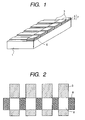
- Fig. 1 is a perspective view showing an example of a light emitting element array which is an exposure device of the present invention.
- reference numeral 1 denotes a substrate, 3 an anode layer, 6 a cathode layer, and 7 an organic compound layer consisting of a hole transport layer 4 and an electron transport layer 5.
- Fig. 2 is an enlarged view of a light emitting portion when seen from the substrate 1 side.
- An overlapped portion between the anode layer 3 and the cathode layer 6 serves as a light emitting portion 8.
- Light is emitted from the light emitting portion by applying voltage between the anode layer 3 and the cathode layer 6 and a light emitting portion having a desired size can be obtained by changing the electrode width of the anode layer 3 or of the cathode layer 6.
- any substrate may be used as the substrate 1 if light emitting elements can be formed on the surface of the substrate.
- a transparent insulating substrate made of glass such as soda-lime glass or a resin film is preferred.
- the material of the anode layer 3 preferably has a large work function, as exemplified by ITO, tin oxide, gold, platinum, palladium, selenium, iridium and copper iodide.
- the material of the cathode layer 6 preferably has a small work function, as exemplified by Mg/Ag, Mg, Al, In and alloys thereof.
- the organic compound layer 7 may be a single layer or consist of a plurality of layers. For example, as shown in Fig. 1, it consists of a hole transport layer 4 into which holes are injected from the anode layer 3 and an electron transport layer 5 into which electrons are injected from the cathode layer 6. In this case, either one of the hole transport layer 4 and the electron transport layer 5 functions as a light emitting layer. A fluorescent layer containing a phosphor may be formed between the hole transport layer 4 and the electron transport layer 5.
- the organic compound layer 7 may be a single mixed layer serving as the hole transport layer 4, electron transport layer 5 and fluorescent layer.
- the hole transport layer 4 may be formed of N,N'-bis(3-methylphenyl)-N,N'-diphenyl-(1,1'-biphenyl)-4,4'-diamine (to be abbreviated as TPD), for instance.
- TPD N,N'-bis(3-methylphenyl)-N,N'-diphenyl-(1,1'-biphenyl)-4,4'-diamine
- TPD N,N'-bis(3-methylphenyl)-N,N'-diphenyl-(1,1'-biphenyl)-4,4'-diamine
- TPD N,N'-bis(3-methylphenyl)-N,N'-diphenyl-(1,1'-biphenyl)-4,4'-diamine
- the following organic materials may be used.
- Inorganic materials such as a-Si and a-SiC may also be used.
- Tris(8-quinolinol) aluminum (to be abbreviated as Alq3), for example, may be used as the electron transport layer 5 and also the following materials may be used.
- Dopant pigments shown below may be doped on the electron transport layer 5 or the hole transport layer 4.
- a dielectric layer is preferably formed between the anode layer 3 and the substrate 1.
- the dielectric layer can increase (or reduce) the reflectance or transmittance of light having a specific wavelength by laminating layers having a different refractive index such as SiO 2 and SiO layers.
- a half mirror may be used to increase (or reduce) the reflectance or transmittance.
- a material that emits light having the same spectral sensitivity as that of a photosensitive member used, such as a photosensitive drum is preferably selected as the material of each layer.
- a glass substrate is used as the transparent insulating substrate 1. Both sides of the glass substrate are washed thoroughly.
- the substrate 1 is covered with a metal mask having a line width of 50 ⁇ m and a pitch of 80 pm and a 100 nm-thick ITO film is formed by a sputtering method as the anode layer 3.
- the film on the entire surface of the substrate it may be etched by photolithography to form a desired pattern.
- TPD and Alq 3 are deposited to a thickness of 50 nm by a vacuum vapor deposition method as the hole transport layer 4 and the electron transport layer 5, respectively.
- the degree of vacuum at the time of deposition is 3 to 4 ⁇ 10 -4 Pa (2 to 3 x 10 -6 Torr) and the film forming speed is 0.2 to 0.3 nm/s.
- the resulting laminate is covered with a metal mask having a line width of 80 pm in such a manner that the metal mask becomes perpendicular to the anode layer 3 and Mg and Ag are co-deposited at a deposition speed ratio of 10:1 to form a 200 nm-thick layer of an alloy of Mg and Ag (10/1) as the cathode layer 6.
- the film forming speed is 1 nm/s.
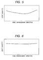
- Fig. 5 is a graph showing an example of the emitted light quantity distribution of the light emitting array produced as described above.
- the quantity of emitted light is small at a central portion and large at both end portions in this example. This is probably because field strength applied to light emitting portions at both end portions becomes higher than that at the central portion and the quantity of light becomes large as there is such a deposited film thickness distribution that the film thickness is larger at the central portion than that at both end portions when the organic compound layer is formed by deposition.
- the emitted light quantity distribution can be improved by reforming a deposition device. However, the emitted light quantity distribution may not be made completely uniform because of other factors.
- the quantity of light emitted from each light emitting element is made uniform by controlling the light emitting area of each light emitting element as shown in Fig. 6.
- each pixel is caused to emit light, the quantity of light emitted from each of all the pixels is measured, and the quantity of light emitted from each light emitting element is made uniform by reducing the light emitting area of a pixel that emits a large quantity of light based on the measurement data.
- Fig. 7 shows examples of the light emitting portion having a reduced light emitting area.
- the light emitting surface is directly irradiated with a laser beam or the like which is shrunk to a small size from the substrate side to give heat or light energy to the organic compound layer so as to modify, for example, melt, evaporate or decompose, the organic compound layer, thereby forming a dark portion 9 which does not emit light and reducing the area of the light emitting portion 8.
- a linear dark portion 9 i.e. a stripe
- a linear dark portion 9 is preferably formed in such a manner that it extends in a direction that is perpendicularly transverse to the direction of rotation of the photosensitive member (direction shown by an arrow in Fig. 7) because this prevents light emitting points from being thinner or a change in the shape of the light emitting portion caused by the formation of the dark portion from exerting an influence upon a latent image on the photosensitive member.
- Fig. 8 shows other examples of the light emitting portion having a reduced light emitting area.
- the dark portion 9 is formed as a spot in the same manner as in Fig. 7 to minimize a change in the shape of the light emitting point. According to these examples, an image is formed on the photosensitive member by a SELFOC lens array "SLA" without being influenced by the dark portion 9 due to the MTF characteristics of SLA.
- Fig. 9 shows still other examples of the light emitting portion having a reduced light emitting area.
- the light emitting surface is directly irradiated with a laser beam or the like which is shrunk to a small size to give heat or light energy to at least one of the anode layer and the cathode layer so as to modify, for example, melt, evaporate or decompose, or cut the anode layer or the cathode layer, thereby forming the dark portion 9.
- the light emitting portion can be trimmed completely by cutting the anode layer or the cathode layer, thereby making it possible to reduce the light emitting area with more certainty.
- Fig. 3 is a schematic structural diagram of an image forming apparatus using electrophotography as an example of the image forming apparatus of the present invention.
- Reference numeral 211 denotes a rotary drum type electrophotographic photosensitive member as an image carrier, 212 electrifying means, 213 developing means, 214 transfer means, 215 fixing means, 216 cleaning means and E the exposure means of the present invention.
- the exposure device E of the present invention is used as the light source of exposure light L.
- the exposure device is connected to a driver.
- DC voltage is applied using the anode layer as a positive pole and the cathode layer as a negative pole, green light emission can be obtained from the light emitting portions and an image can be formed on the photosensitive member 211. Thus, a good image can be obtained.
- the photosensitive member 211 is uniformly electrified by the electrifying means 212.
- the electrified side of the photosensitive member 211 is exposed to light L by the exposure device E in accordance with time series electric digital pixel signals which are objective outputted image information to form an electrostatic latent image corresponding to the objective image information on the peripheral surface of the photosensitive member 211.
- This electrostatic latent image is developed as a toner image by the developing means 213 which uses an insulating toner.
- a transfer material P is supplied from a paper feeding unit (not shown) as a recording material and introduced at a predetermined timing into a press-contact nip portion (transfer portion) T between the photosensitive member 211 and contact transfer means which is contacted to the photosensitive member with predetermined pressure to transfer the toner image by applying predetermined transfer bias voltage.
- the transfer material P to which the toner image has been transferred is separated from the surface of the photosensitive member 211, introduced into the fixing means 215 of a heat fixing system or the like to fix the toner image and discharged to the outside of the device as an image formed product (print).
- the surface of the photosensitive member after the transfer of the toner image to the transfer material P is cleaned by the cleaning means 216 to remove adhered contaminants such as the residual toner and used repeatedly to form an image thereon.
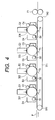
- Fig. 4 is a schematic structural diagram of a multi-color image forming apparatus using electrophotography as another example of the image forming apparatus of the present invention.
- C1 to C4 are electrifying means, D1 to D4 developing means, E1 to E4 the exposure means of the present invention, S1 to S4 developing sleeves, T1 to T4 transfer blades, TR1 and TR2 rollers, TF1 transfer belt, P transfer paper, Fl fixing unit, and 301 to 304 rotary drum type electrophotographic photosensitive member.
- the transfer paper P is carried in a direction shown by an arrow, guided onto the transfer belt TF1 laid on the rollers TR1 and TR2, and moved to a black transfer position set such that the paper is supported between the photosensitive member 301 and the transfer blade T1 by the transfer belt TF1.
- the photosensitive member 301 has a desired black toner image by an electrophotographic process with the electrifying means C1, the exposure means E1 and the developing sleeve S1 of the developing means D1 arranged on the periphery of a drum and the black toner image is transferred to the transfer paper P.
- the transfer paper P is moved by the transfer belt TTF1 to a cyan transfer position set such that the paper is supported between the photosensitive member 302 and the transfer blade T2, a magenta transfer position set such that the paper is supported between the photosensitive member 303 and the transfer blade T3, and a yellow transfer position set such that it is supported between the photosensitive member 304 and the transfer blade T4 so that a cyan toner image, magenta toner image and yellow toner image are transferred at the respective transfer positions by the same means as that of the black transfer position.
- the transfer paper P on which multi-color recording is carried out by the above process is supplied to the fixing unit F1 to fix the images, thereby making it possible to obtain a desired multi-color image.
- the present invention is most effective when the number of light emitting pixels is increased to achieve high density.
Claims (11)
- Groupement d'éléments émettant de la lumière comprenant une pluralité d'éléments émettant de la lumière comportant chacun une paire d'électrodes (3, 6) et une couche émettant de la lumière (7 : 4, 5) disposée entre la paire d'électrodes, où les zones d'émission de lumière (8) des éléments émettant de la lumière respectifs sont limitées par les zones de chevauchement des paires respectives d'électrodes et la direction d'émission de lumière est transversale par rapport au plan de la couche émettant de la lumière de chaque élément émettant de la lumière,
lequel groupement d'éléments émettant de la lumière est caractérisé en ce que :lesdits éléments émettant de la lumière (3, 6, 7) diffèrent en ce qui concerne la zone d'émission de lumière efficace (8) de façon à rendre uniformes les quantités d'émission de lumière de ceux-ci. - Groupement d'éléments émettant de la lumière selon la revendication 1, dans lequel lesdits éléments émettant de la lumière (3, 6, 7) diffèrent en ce qui concerne la zone d'émission de lumière efficace (8), en ce que la couche émettant de la lumière (7 : 4, 5) d'au moins l'un des éléments émettant de la lumière (3, 6, 7) comporte une ou plusieurs parties modifiées (9), qui n'émettent pas de lumière.
- Groupement d'éléments émettant de la lumière selon la revendication 2, dans lequel ladite couche émettant de la lumière (7 : 4, 5) dudit au moins un des éléments émettant de la lumière (3, 6, 7) comporte une partie ou des parties de bande n'émettant pas de lumière (9).
- Groupement d'éléments émettant de la lumière selon la revendication 2, dans lequel ladite couche émettant de la lumière (7 : 4, 5) dudit au moins un des éléments émettant de la lumière (3, 6, 7) comporte une partie ou des parties de point n'émettant pas de lumière (9).
- Groupement d'éléments émettant de la lumière selon la revendication 1, dans lequel lesdits éléments émettant de la lumière (3, 6, 7) diffèrent en ce qui concerne la zone d'émission de lumière efficace (8), en ce que la zone de chevauchement d'au moins une paire d'électrodes est différente des autres zones de chevauchement desdites autres paires d'électrodes.
- Groupement d'éléments émettant de la lumière selon l'une quelconque des revendications précédentes, dans lequel :ladite pluralité d'éléments émettant de la lumière (3, 6, 7) sont disposés sur un substrat commun (1) ;une première électrode (3) de chaque paire d'électrodes (3, 6) est disposée plus près du substrat et celles-ci sont séparées l'une de l'autre pour chaque élément, tandis que l'autre électrode (6) de chaque paire d'électrodes (3, 6) est une électrode commune (6) disposée plus loin par rapport au substrat et s'étendant sur les électrodes séparées respectives (3).
- Dispositif de formation d'image qui comprend un élément photosensible électrophotographique (211 ; 301, 302, 303, 304) et un groupement d'éléments émettant de la lumière (E ; E1 à E4) agencé pour illuminer ledit élément photosensible électrophotographique afin de former une image latente sur celui-ci, où ledit groupement d'éléments émettant de la lumière est tel que revendiqué dans l'une quelconque des revendications précédentes.
- Dispositif de formation d'image selon la revendication 7, dans lequel ledit élément photosensible électrophotographique est du type à tambour rotatif, ledit groupement d'éléments émettant de la lumière est tel que revendiqué dans la revendication 3, et la direction d'extension de ladite partie ou desdites parties de bande n'émettant pas de lumière est perpendiculairement transversale à la direction de rotation dudit élément photosensible électrophotographique.
- Procédé de fabrication du groupement d'éléments émettant de la lumière selon la revendication 1, exécuté en :fournissant le groupement comprenant une pluralité d'éléments émettant de la lumière (3, 6, 7), comprenant chacun une paire d'électrodes (3, 6) et une couche émettant de la lumière (7) comprenant un composé organique pris en sandwich entre la paire d'électrodes ;mesurant la répartition de quantité de lumière émise dudit groupement ; etajustant la zone (8) de la partie émettant de la lumière des éléments émettant de la lumière du groupement, en fonction des résultats de la mesure mentionnée précédemment, afin d'équilibrer la répartition de quantité de lumière émise du groupement.
- Procédé selon la revendication 9, dans lequel ledit ajustage est exécuté par rayonnement laser, dont l'effet consiste à faire fondre localement, faire évaporer ou faire se décomposer le composé organique de couche émettant de la lumière dans une partie de ladite couche émettant de la lumière.
- Procédé selon la revendication 9, dans lequel ledit ajustage est exécuté par rayonnement laser, dont l'effet consiste à faire fondre localement, faire évaporer, faire se décomposer en partie ou découper l'une ou l'autre des électrodes d'au moins l'une des paires d'électrodes.
Applications Claiming Priority (2)
| Application Number | Priority Date | Filing Date | Title |
|---|---|---|---|
| JP30050298 | 1998-10-22 | ||
| JP30050298A JP3302332B2 (ja) | 1998-10-22 | 1998-10-22 | 露光装置及び画像形成装置 |
Publications (3)
| Publication Number | Publication Date |
|---|---|
| EP1009046A2 EP1009046A2 (fr) | 2000-06-14 |
| EP1009046A3 EP1009046A3 (fr) | 2000-11-22 |
| EP1009046B1 true EP1009046B1 (fr) | 2006-05-24 |
Family
ID=17885598
Family Applications (1)
| Application Number | Title | Priority Date | Filing Date |
|---|---|---|---|
| EP99308289A Expired - Lifetime EP1009046B1 (fr) | 1998-10-22 | 1999-10-20 | Rangée d'éléments à électroluminescence, procédé de fabrication de la rangée et appareil de formation d'images |
Country Status (4)
| Country | Link |
|---|---|
| US (1) | US6344661B1 (fr) |
| EP (1) | EP1009046B1 (fr) |
| JP (1) | JP3302332B2 (fr) |
| DE (1) | DE69931456D1 (fr) |
Families Citing this family (12)
| Publication number | Priority date | Publication date | Assignee | Title |
|---|---|---|---|---|
| US6982813B2 (en) * | 2000-02-16 | 2006-01-03 | Minolta Co., Ltd. | Light quantity correction method for exposing device, and image forming device |
| JP3883770B2 (ja) | 2000-03-07 | 2007-02-21 | パイオニア株式会社 | 発光素子の製造方法 |
| US6900590B2 (en) * | 2000-10-17 | 2005-05-31 | Samsung Sdi Co., Ltd. | Organic electroluminescent device having non-continuous metal auxiliary electrodes |
| PL354113A1 (en) * | 2001-05-25 | 2002-12-02 | Michel Tramontana | Electroluminescent system and apparatus used in manufacturing such system |
| US7858403B2 (en) * | 2001-10-31 | 2010-12-28 | Cree, Inc. | Methods and systems for fabricating broad spectrum light emitting devices |
| US7515166B2 (en) | 2002-12-27 | 2009-04-07 | Seiko Epson Corporation | Line head and image forming apparatus using the same |
| JP2006269108A (ja) * | 2005-03-22 | 2006-10-05 | Hitachi Displays Ltd | 有機発光表示装置及びその欠陥画素の修復方法 |
| JP4981371B2 (ja) * | 2006-06-28 | 2012-07-18 | ハリソン東芝ライティング株式会社 | 有機el素子 |
| US7863807B2 (en) * | 2006-08-09 | 2011-01-04 | Tpo Displays Corp. | System for displaying images and method for fabricating the same |
| US7955875B2 (en) * | 2008-09-26 | 2011-06-07 | Cree, Inc. | Forming light emitting devices including custom wavelength conversion structures |
| JP5604817B2 (ja) * | 2009-06-25 | 2014-10-15 | 富士ゼロックス株式会社 | 発光素子、発光素子アレイ、露光ヘッド、露光装置、および画像形成装置 |
| CN110767831B (zh) * | 2018-12-28 | 2022-10-04 | 昆山国显光电有限公司 | 透明oled基板、显示面板、阵列基板、显示屏及显示装置 |
Family Cites Families (8)
| Publication number | Priority date | Publication date | Assignee | Title |
|---|---|---|---|---|
| JPS60198873A (ja) | 1984-03-23 | 1985-10-08 | Mitsubishi Electric Corp | 発光ダイオ−ドアレイ |
| JPH0390370A (ja) * | 1989-09-04 | 1991-04-16 | Tokyo Electric Co Ltd | ラインヘッドの光出力調整方法 |
| US5475417A (en) | 1991-10-25 | 1995-12-12 | Rohm Co., Ltd. | LED array printhead and method of adjusting light luminance of same |
| JPH05330135A (ja) | 1992-05-29 | 1993-12-14 | Toshiba Corp | 画像形成装置 |
| US5482896A (en) | 1993-11-18 | 1996-01-09 | Eastman Kodak Company | Light emitting device comprising an organic LED array on an ultra thin substrate and process for forming same |
| JPH0890832A (ja) | 1994-09-27 | 1996-04-09 | Oki Electric Ind Co Ltd | 発光素子アレイおよび光学ヘッド |
| US6111357A (en) * | 1998-07-09 | 2000-08-29 | Eastman Kodak Company | Organic electroluminescent display panel having a cover with radiation-cured perimeter seal |
| US6266074B1 (en) * | 1998-10-22 | 2001-07-24 | Canon Kabushiki Kaisha | Light emitting apparatus with temperature control, exposure apparatus, and image forming apparatus |
-
1998
- 1998-10-22 JP JP30050298A patent/JP3302332B2/ja not_active Expired - Fee Related
-
1999
- 1999-10-19 US US09/420,390 patent/US6344661B1/en not_active Expired - Lifetime
- 1999-10-20 DE DE69931456T patent/DE69931456D1/de not_active Expired - Lifetime
- 1999-10-20 EP EP99308289A patent/EP1009046B1/fr not_active Expired - Lifetime
Also Published As
| Publication number | Publication date |
|---|---|
| JP2000127492A (ja) | 2000-05-09 |
| EP1009046A3 (fr) | 2000-11-22 |
| EP1009046A2 (fr) | 2000-06-14 |
| DE69931456D1 (de) | 2006-06-29 |
| US6344661B1 (en) | 2002-02-05 |
| JP3302332B2 (ja) | 2002-07-15 |
Similar Documents
| Publication | Publication Date | Title |
|---|---|---|
| US6504565B1 (en) | Light-emitting device, exposure device, and image forming apparatus | |
| EP1009046B1 (fr) | Rangée d'éléments à électroluminescence, procédé de fabrication de la rangée et appareil de formation d'images | |
| US6583805B2 (en) | Exposure unit for image forming apparatus using electrophotographic system, and electrophotographic image forming apparatus | |
| JP4143181B2 (ja) | 露光装置及び画像形成装置 | |
| JP4233196B2 (ja) | 露光装置 | |
| US6661445B2 (en) | Exposure apparatus with an array of light emitting devices | |
| US6236416B1 (en) | Image forming apparatus featuring a plurality of light emission elements on a single chip | |
| US7283149B2 (en) | Optical head and image forming apparatus employing the same | |
| US6266074B1 (en) | Light emitting apparatus with temperature control, exposure apparatus, and image forming apparatus | |
| JP2003341140A (ja) | 光学ヘッドおよびそれを用いた画像形成装置 | |
| JPH1055890A (ja) | 有機elアレイ | |
| JP4154045B2 (ja) | 画像形成装置 | |
| JP4143180B2 (ja) | 多色画像形成装置 | |
| JP2000127491A (ja) | 露光装置及び画像形成装置 | |
| JP4257505B2 (ja) | 画像形成装置および画像形成方法 | |
| JP4541535B2 (ja) | 光ヘッド用有機発光ダイオードアレイ | |
| JP3302330B2 (ja) | 発光装置、露光装置及び画像形成装置 | |
| JP2000094741A (ja) | 発光装置、露光装置及び画像形成装置 | |
| JP3302329B2 (ja) | 発光装置、露光装置及び画像形成装置 | |
| JP2000289249A (ja) | 露光装置及びそれを用いた画像形成装置 | |
| JP2004050816A (ja) | 画像形成装置および画像形成方法 | |
| JP2000353590A (ja) | 有機el発光素子 | |
| JP2002187306A (ja) | 有機発光ダイオードアレイ | |
| JPS59109071A (ja) | 電子写真式プリンタ−の光書込みヘツド | |
| JPS59102259A (ja) | 電子写真記録装置 |
Legal Events
| Date | Code | Title | Description |
|---|---|---|---|
| PUAI | Public reference made under article 153(3) epc to a published international application that has entered the european phase |
Free format text: ORIGINAL CODE: 0009012 |
|
| AK | Designated contracting states |
Kind code of ref document: A2 Designated state(s): DE FR GB |
|
| AX | Request for extension of the european patent |
Free format text: AL;LT;LV;MK;RO;SI |
|
| PUAL | Search report despatched |
Free format text: ORIGINAL CODE: 0009013 |
|
| AK | Designated contracting states |
Kind code of ref document: A3 Designated state(s): AT BE CH CY DE DK ES FI FR GB GR IE IT LI LU MC NL PT SE |
|
| AX | Request for extension of the european patent |
Free format text: AL;LT;LV;MK;RO;SI |
|
| RIC1 | Information provided on ipc code assigned before grant |
Free format text: 7H 01L 51/20 A, 7H 05B 33/10 B, 7B 41J 2/45 B |
|
| 17P | Request for examination filed |
Effective date: 20010409 |
|
| AKX | Designation fees paid |
Free format text: DE FR GB |
|
| 17Q | First examination report despatched |
Effective date: 20040810 |
|
| GRAP | Despatch of communication of intention to grant a patent |
Free format text: ORIGINAL CODE: EPIDOSNIGR1 |
|
| RTI1 | Title (correction) |
Free format text: LIGHT EMITTING ELEMENT ARRAY, METHOD OF FORMING THE ARRAY AND IMAGE FORMING APPARATUS |
|
| GRAS | Grant fee paid |
Free format text: ORIGINAL CODE: EPIDOSNIGR3 |
|
| GRAA | (expected) grant |
Free format text: ORIGINAL CODE: 0009210 |
|
| AK | Designated contracting states |
Kind code of ref document: B1 Designated state(s): DE FR GB |
|
| REG | Reference to a national code |
Ref country code: GB Ref legal event code: FG4D |
|
| RIC1 | Information provided on ipc code assigned before grant |
Ipc: B41J 2/45 20060101ALI20060404BHEP Ipc: H05B 33/10 20060101ALI20060404BHEP Ipc: H01L 51/50 20060101AFI20060404BHEP |
|
| REF | Corresponds to: |
Ref document number: 69931456 Country of ref document: DE Date of ref document: 20060629 Kind code of ref document: P |
|
| PG25 | Lapsed in a contracting state [announced via postgrant information from national office to epo] |
Ref country code: DE Free format text: LAPSE BECAUSE OF FAILURE TO SUBMIT A TRANSLATION OF THE DESCRIPTION OR TO PAY THE FEE WITHIN THE PRESCRIBED TIME-LIMIT Effective date: 20060825 |
|
| PLBE | No opposition filed within time limit |
Free format text: ORIGINAL CODE: 0009261 |
|
| STAA | Information on the status of an ep patent application or granted ep patent |
Free format text: STATUS: NO OPPOSITION FILED WITHIN TIME LIMIT |
|
| 26N | No opposition filed |
Effective date: 20070227 |
|
| EN | Fr: translation not filed | ||
| PG25 | Lapsed in a contracting state [announced via postgrant information from national office to epo] |
Ref country code: FR Free format text: LAPSE BECAUSE OF FAILURE TO SUBMIT A TRANSLATION OF THE DESCRIPTION OR TO PAY THE FEE WITHIN THE PRESCRIBED TIME-LIMIT Effective date: 20070309 |
|
| PG25 | Lapsed in a contracting state [announced via postgrant information from national office to epo] |
Ref country code: FR Free format text: LAPSE BECAUSE OF FAILURE TO SUBMIT A TRANSLATION OF THE DESCRIPTION OR TO PAY THE FEE WITHIN THE PRESCRIBED TIME-LIMIT Effective date: 20060524 |
|
| PGFP | Annual fee paid to national office [announced via postgrant information from national office to epo] |
Ref country code: GB Payment date: 20151026 Year of fee payment: 17 |
|
| GBPC | Gb: european patent ceased through non-payment of renewal fee |
Effective date: 20161020 |
|
| PG25 | Lapsed in a contracting state [announced via postgrant information from national office to epo] |
Ref country code: GB Free format text: LAPSE BECAUSE OF NON-PAYMENT OF DUE FEES Effective date: 20161020 |