EP0998036A1 - Filtre de multiplexage/derivation - Google Patents
Filtre de multiplexage/derivation Download PDFInfo
- Publication number
- EP0998036A1 EP0998036A1 EP99939861A EP99939861A EP0998036A1 EP 0998036 A1 EP0998036 A1 EP 0998036A1 EP 99939861 A EP99939861 A EP 99939861A EP 99939861 A EP99939861 A EP 99939861A EP 0998036 A1 EP0998036 A1 EP 0998036A1
- Authority
- EP
- European Patent Office
- Prior art keywords
- port
- weight
- multiplexer
- demultiplexer
- resonant circuit
- Prior art date
- Legal status (The legal status is an assumption and is not a legal conclusion. Google has not performed a legal analysis and makes no representation as to the accuracy of the status listed.)
- Granted
Links
Images


Classifications
-
- H—ELECTRICITY
- H03—ELECTRONIC CIRCUITRY
- H03H—IMPEDANCE NETWORKS, e.g. RESONANT CIRCUITS; RESONATORS
- H03H7/00—Multiple-port networks comprising only passive electrical elements as network components
- H03H7/01—Frequency selective two-port networks
- H03H7/17—Structural details of sub-circuits of frequency selective networks
- H03H7/1741—Comprising typical LC combinations, irrespective of presence and location of additional resistors
- H03H7/1775—Parallel LC in shunt or branch path
-
- C—CHEMISTRY; METALLURGY
- C03—GLASS; MINERAL OR SLAG WOOL
- C03C—CHEMICAL COMPOSITION OF GLASSES, GLAZES OR VITREOUS ENAMELS; SURFACE TREATMENT OF GLASS; SURFACE TREATMENT OF FIBRES OR FILAMENTS MADE FROM GLASS, MINERALS OR SLAGS; JOINING GLASS TO GLASS OR OTHER MATERIALS
- C03C10/00—Devitrified glass ceramics, i.e. glass ceramics having a crystalline phase dispersed in a glassy phase and constituting at least 50% by weight of the total composition
- C03C10/0036—Devitrified glass ceramics, i.e. glass ceramics having a crystalline phase dispersed in a glassy phase and constituting at least 50% by weight of the total composition containing SiO2, Al2O3 and a divalent metal oxide as main constituents
-
- C—CHEMISTRY; METALLURGY
- C03—GLASS; MINERAL OR SLAG WOOL
- C03C—CHEMICAL COMPOSITION OF GLASSES, GLAZES OR VITREOUS ENAMELS; SURFACE TREATMENT OF GLASS; SURFACE TREATMENT OF FIBRES OR FILAMENTS MADE FROM GLASS, MINERALS OR SLAGS; JOINING GLASS TO GLASS OR OTHER MATERIALS
- C03C14/00—Glass compositions containing a non-glass component, e.g. compositions containing fibres, filaments, whiskers, platelets, or the like, dispersed in a glass matrix
- C03C14/004—Glass compositions containing a non-glass component, e.g. compositions containing fibres, filaments, whiskers, platelets, or the like, dispersed in a glass matrix the non-glass component being in the form of particles or flakes
-
- C—CHEMISTRY; METALLURGY
- C03—GLASS; MINERAL OR SLAG WOOL
- C03C—CHEMICAL COMPOSITION OF GLASSES, GLAZES OR VITREOUS ENAMELS; SURFACE TREATMENT OF GLASS; SURFACE TREATMENT OF FIBRES OR FILAMENTS MADE FROM GLASS, MINERALS OR SLAGS; JOINING GLASS TO GLASS OR OTHER MATERIALS
- C03C8/00—Enamels; Glazes; Fusion seal compositions being frit compositions having non-frit additions
- C03C8/14—Glass frit mixtures having non-frit additions, e.g. opacifiers, colorants, mill-additions
-
- H—ELECTRICITY
- H03—ELECTRONIC CIRCUITRY
- H03H—IMPEDANCE NETWORKS, e.g. RESONANT CIRCUITS; RESONATORS
- H03H7/00—Multiple-port networks comprising only passive electrical elements as network components
- H03H7/01—Frequency selective two-port networks
- H03H7/0115—Frequency selective two-port networks comprising only inductors and capacitors
-
- H—ELECTRICITY
- H03—ELECTRONIC CIRCUITRY
- H03H—IMPEDANCE NETWORKS, e.g. RESONANT CIRCUITS; RESONATORS
- H03H7/00—Multiple-port networks comprising only passive electrical elements as network components
- H03H7/01—Frequency selective two-port networks
- H03H7/075—Ladder networks, e.g. electric wave filters
-
- H—ELECTRICITY
- H03—ELECTRONIC CIRCUITRY
- H03H—IMPEDANCE NETWORKS, e.g. RESONANT CIRCUITS; RESONATORS
- H03H7/00—Multiple-port networks comprising only passive electrical elements as network components
- H03H7/01—Frequency selective two-port networks
- H03H7/17—Structural details of sub-circuits of frequency selective networks
- H03H7/1741—Comprising typical LC combinations, irrespective of presence and location of additional resistors
- H03H7/1791—Combined LC in shunt or branch path
-
- H—ELECTRICITY
- H03—ELECTRONIC CIRCUITRY
- H03H—IMPEDANCE NETWORKS, e.g. RESONANT CIRCUITS; RESONATORS
- H03H7/00—Multiple-port networks comprising only passive electrical elements as network components
- H03H7/46—Networks for connecting several sources or loads, working on different frequencies or frequency bands, to a common load or source
-
- H—ELECTRICITY
- H03—ELECTRONIC CIRCUITRY
- H03H—IMPEDANCE NETWORKS, e.g. RESONANT CIRCUITS; RESONATORS
- H03H1/00—Constructional details of impedance networks whose electrical mode of operation is not specified or applicable to more than one type of network
- H03H2001/0021—Constructional details
- H03H2001/0085—Multilayer, e.g. LTCC, HTCC, green sheets
Definitions
- the present invention relates to a multiplexer/demultiplexer for use in mobile communication devices such as portable telephone.
- FIG. 14 represents a circuit construction of a conventional multiplexer/demultiplexer.
- the circuit is comprised of a low-pass filter 101, a high-pass filter 102, phase shifters 103, 104, input terminals 105, 106, and an output terminal 107.
- low-pass filter 101 and high-pass filter 102 are configured as ⁇ -shaped 3-stage circuits.
- phase shifters 103, 104 are comprised of a transmission line such as a strip line.
- the present invention is directed to providing an easy-to-miniaturize, low loss, high-performance multiplexer/demultiplexer.
- the multiplexer/demultiplexer of the present invention includes a first to a third ports each externally terminated with a pure resistance, in which the second port is made to be a common port by connecting between the first port and the ground a first resonant circuit which makes serial resonance at a frequency within a first frequency band or in its proximity, and further connecting an inductive element in series between the first port and the second port, and connecting between the third port and the ground a second resonant circuit which makes serial resonance at a frequency within a second frequency band which is different from the first frequency band or in its proximity, and by further connecting a capacitive element in series between the third port and the second port.
- FIG. 1 is a circuit diagram of a multiplexer/demultiplexer in the first exemplary embodiment of the present invention.
- numerals 1, 2, 3 are an input-output port (first port) for a low-frequency band, an input-output port (second port) for a high-frequency band, and a common input-output port (third port), respectively.
- Numerals 4, 6, 9 are capacitive elements, and numerals 5, 7, 8 are inductive elements.
- serial resonant circuit 30 resonates in the pass band from second port 2 to third port 3
- serial resonant circuit 31 resonates in the pass band from first port 1 to third port 3.
- the circuit functions as an equivalent circuit represented by FIG. 2, namely, a ⁇ -type low-pass filter.
- serial resonant circuit 30 functions equivalently to a capacitive element 28 as the frequency is lower than its resonant point.
- the circuit functions as an equivalent circuit represented by FIG. 3, namely, a ⁇ -type high-pass filter.
- serial resonant circuit 31 functions equivalently to an inductive element 29 as the frequency is higher than its resonant point.
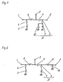
- FIG. 4 is a circuit diagram of a multiplexer/demultiplexer in a second exemplary embodiment of the present invention.
- the circuit of this embodiment is one in which a serial resonant circuit 32 comprising a capacitive element 10 and an inductive element 11 has been added between serial resonant circuit 31 and second port 2 of the first exemplary embodiment.
- the resonant point of serial resonant circuit 32 is set at a frequency about twice the pass band frequency from second port 2 to third port 3 thus enabling efficient elimination of harmonics from an amplifier and the like to be connected to second port 2 (providing an attenuating pole to eliminate high-frequency spurious components) and providing a multiplexer/demultiplexer with further enhanced performance.
- serial resonant circuit 32 by connecting serial resonant circuit 32 between serial resonant circuit 31 and second port 2 as illustrated in FIG. 4, it is possible to restrain deterioration of the pass characteristics from first port 1 to third port 3 due to the influence of serial resonant circuit 32.
- FIG. 5 is a circuit diagram of a multiplexer/demultiplexer in the third exemplary embodiment of the present invention.
- the circuit of this embodiment is one in which a capacitive element 12 has been connected in parallel with inductive element 7 of the first exemplary embodiment and furthermore the serial resonant point of a circuit 33 comprising capacitive elements 6, 12 and inductive element 7 has been set to be in the pass band from first port 1 to third port 3.
- FIG. 6 is a circuit diagram of a multiplexer/demultiplexer in the fourth exemplary embodiment of the present invention.
- the circuit of this embodiment is one in which an inductive element 13 and a capacitive element 14 have been respectively connected in series and in parallel between serial resonant circuit 31 and second port 2 of the first exemplary embodiment.
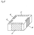
- the first to fourth exemplary embodiments can be implemented by laminating dielectric sheets on which electrodes have been printed as illustrated in FIG. 7 and FIG. 8.
- FIG. 7 illustrates internal construction of the present embodiment where numeral 19 is a dielectric sheet, numerals 20, 22, 24 are grounding layers printed with a grounding electrode 25, numeral 21 is a group of sheets inside which a capacitive element 4 and inductive elements 5, 8 have been printed and laminated, numeral 23 is a group of sheets inside which a capacitive element and an inductive element have been printed and laminated.
- Numeral 26 is a lead electrode of inductive element 8 on the side of port 3 while numeral 27 is a lead electrode of capacitive element 9 on the side of port 3. Lead electrodes 26, 27 are so disposed as will come one on top of the other when stacked.
- FIG. 8 is a perspective view of the laminated multiplexer/demultiplexer illustrated in FIG. 7.
- numerals 15, 16 are input terminals
- numeral 17 is a grounding terminal
- numeral 18 is an output terminal.
- numeral 18 is a terminal electrode corresponding to third port 3. As has been described above, it forms an external terminal at the point it is taken out. External terminal 18 is also a connecting point for inductive element 8 and capacitive element 9.
- a glass ceramic material consisting of a mixture of 55-65 % by weight of a glass composition powders consisting of 40-50 % by weight SiO 2 , 30-40 % by weight BaO, 3-8 % by weight Al 2 O 3 , 8-12% by weight La 2 O 3 , and 3-6 % by weight B 2 O 3 , and 45-35 % by weight forsterite (Mg 2 SiO 4 ); or a glass ceramic material consisting of a mixture of 50-65 % by weight glass composition powders consisting of 40-50 % by weight SiO 2 , 30-40 % by weight BaO, 3-8 % by weight Al 2 O 3 , 8-12 % by weight La 2 O 3 , and 3-6 % by weight B 2 O 3 , and 50-35 % by weight forsterite (Mg 2 SiO 4 ) can be used after adding 0.2-5 % by weight CuO equivalent of copper oxide as a sub-component.
- the values of elements (on the order of 2 to 10 nH for inductive elements, and 2 to 10 pF for capacitive elements) as used in the exemplary embodiment can be efficiently realized with superior high-frequency characteristics and a low loss.
- use of these materials makes it possible to realize a multiplexer/demultiplexer which is superior in mounting reliability especially onto resin substrates because of a high anti-breakage strength and an adequately high thermal expansion coefficient, easy of manufacturing because the content of boron oxides in the glass powders is small, and the electrical characteristics at high frequencies are superior.
- FIG. 10 is a circuit diagram of a multiplexer/demultiplexer in the fifth exemplary embodiment of the present invention.
- the circuit of this embodiment is one in which connecting relationships in the first exemplary embodiment of capacitive element 4 and inductive element 5, and capacitive element 6 and inductive element 7 have been reversed, and in which more pronounced effect is obtained when applied to a high-frequency circuit in the GHz range or above.
- parasitic capacitances 34(a) - 34(d) exist at both ends of each of the inductive elements and the capacitive elements as illustrated in FIG. 11(a) and (b), they have to be taken into account when designing a circuit.
- the parasitic capacitances are as shown in FIG. 12(a), which can be further summarized as in FIG. 12(b).
- FIG. 13(a) when parasitic capacitances of the first exemplary embodiment are considered for the purpose of comparison, they are as shown in FIG. 13(a), which can be further summarized as in FIG. 13(b).
- unnecessary parallel resonant circuits 36, 37 are actually formed by inductive elements 5, 7 and a parasitic capacitance 35.
- the parallel resonant circuits 36, 37 comprise parasitic capacitance 35, they are uncontrollable and cause a discrepancy between the designed characteristics and the characteristics that are actually realized by fabrication, presenting a serious difficulty in taking measures.
- the present invention provides a small and high performance multiplexer/demultiplexer with ease.
Landscapes
- Chemical & Material Sciences (AREA)
- Engineering & Computer Science (AREA)
- Materials Engineering (AREA)
- Life Sciences & Earth Sciences (AREA)
- Chemical Kinetics & Catalysis (AREA)
- General Chemical & Material Sciences (AREA)
- Geochemistry & Mineralogy (AREA)
- Organic Chemistry (AREA)
- Ceramic Engineering (AREA)
- Dispersion Chemistry (AREA)
- Power Engineering (AREA)
- Crystallography & Structural Chemistry (AREA)
- Filters And Equalizers (AREA)
Applications Claiming Priority (3)
| Application Number | Priority Date | Filing Date | Title |
|---|---|---|---|
| JP6660798 | 1998-03-17 | ||
| JP6660798 | 1998-03-17 | ||
| PCT/JP1999/001285 WO1999048199A1 (fr) | 1998-03-17 | 1999-03-16 | Filtre de multiplexage/derivation |
Publications (3)
| Publication Number | Publication Date |
|---|---|
| EP0998036A1 true EP0998036A1 (fr) | 2000-05-03 |
| EP0998036A4 EP0998036A4 (fr) | 2001-02-21 |
| EP0998036B1 EP0998036B1 (fr) | 2003-11-05 |
Family
ID=13320769
Family Applications (1)
| Application Number | Title | Priority Date | Filing Date |
|---|---|---|---|
| EP99939861A Expired - Lifetime EP0998036B1 (fr) | 1998-03-17 | 1999-03-16 | Filtre de multiplexage/derivation |
Country Status (4)
| Country | Link |
|---|---|
| US (1) | US6335663B1 (fr) |
| EP (1) | EP0998036B1 (fr) |
| DE (1) | DE69912563T2 (fr) |
| WO (1) | WO1999048199A1 (fr) |
Cited By (2)
| Publication number | Priority date | Publication date | Assignee | Title |
|---|---|---|---|---|
| WO2010092308A1 (fr) * | 2009-02-12 | 2010-08-19 | Thomson Licensing | Reseau de filtrage en technologie silicium si-hr |
| US8170511B2 (en) * | 2006-08-14 | 2012-05-01 | St-Ericsson Sa | Equalizer system for emitting a quasi-constant power output RF signal in a frequency band |
Families Citing this family (9)
| Publication number | Priority date | Publication date | Assignee | Title |
|---|---|---|---|---|
| JP4505777B2 (ja) * | 2001-02-26 | 2010-07-21 | 日立金属株式会社 | 周波数分波回路、およびマルチバンドアンテナスイッチ積層モジュール複合部品 |
| JP2004349740A (ja) * | 2003-05-14 | 2004-12-09 | Advantest Corp | 入力信号処理装置、高周波成分取得方法および低周波成分取得方法 |
| JP4669722B2 (ja) * | 2005-03-18 | 2011-04-13 | 太陽誘電株式会社 | 共振回路、フィルタ回路、多層基板並びに回路モジュール |
| JP5081742B2 (ja) * | 2007-06-29 | 2012-11-28 | 日本電波工業株式会社 | アンテナ分波器 |
| JP4561931B2 (ja) * | 2007-12-26 | 2010-10-13 | 株式会社村田製作所 | アンテナ装置および無線icデバイス |
| JP5549820B2 (ja) * | 2012-03-28 | 2014-07-16 | Tdk株式会社 | トリプレクサ |
| CN109301413B (zh) | 2015-04-29 | 2021-07-16 | 上海华为技术有限公司 | 一种多工器的输入输出装置及多工器 |
| US10425061B1 (en) * | 2018-10-11 | 2019-09-24 | Qorvo Us, Inc. | Wireless communication circuitry |
| CN117242699A (zh) * | 2021-05-14 | 2023-12-15 | 三菱电机株式会社 | 多赫蒂放大器 |
Family Cites Families (12)
| Publication number | Priority date | Publication date | Assignee | Title |
|---|---|---|---|---|
| JPS5797715A (en) * | 1980-12-10 | 1982-06-17 | Fujitsu Ltd | Lc filter |
| JPS61214625A (ja) | 1985-03-19 | 1986-09-24 | Tokyo Electric Co Ltd | アンテナ結合回路 |
| JPH068189B2 (ja) * | 1985-03-26 | 1994-02-02 | 株式会社東芝 | 酸化物誘電体材料 |
| JPS6423123A (en) | 1987-07-17 | 1989-01-25 | Shimadzu Corp | Electronic balance |
| JPS6423123U (fr) * | 1987-07-30 | 1989-02-07 | ||
| JPH0728161B2 (ja) | 1989-10-06 | 1995-03-29 | 三菱電機株式会社 | マイクロ波半導体スイッチ |
| JPH04207806A (ja) | 1990-11-30 | 1992-07-29 | Murata Mfg Co Ltd | デュプレクサ |
| JP3123201B2 (ja) | 1992-03-31 | 2001-01-09 | ソニー株式会社 | ディスクカートリッジ用ケース |
| JPH07122905A (ja) | 1993-10-26 | 1995-05-12 | Murata Mfg Co Ltd | 高周波フィルタ |
| JPH09153842A (ja) | 1995-11-30 | 1997-06-10 | Murata Mfg Co Ltd | 高周波部品 |
| DE69734846T2 (de) * | 1996-02-27 | 2006-08-31 | Hitachi Metals, Ltd. | Frequenzweiche für Zweiband-Mobilfunkendgeräte |
| EP0837517B1 (fr) * | 1996-10-18 | 2004-01-28 | Matsushita Electric Industrial Co., Ltd. | Filtre diélectrique statifié et dispositif de communication |
-
1999
- 1999-03-16 US US09/423,977 patent/US6335663B1/en not_active Expired - Fee Related
- 1999-03-16 WO PCT/JP1999/001285 patent/WO1999048199A1/fr active IP Right Grant
- 1999-03-16 EP EP99939861A patent/EP0998036B1/fr not_active Expired - Lifetime
- 1999-03-16 DE DE69912563T patent/DE69912563T2/de not_active Expired - Fee Related
Non-Patent Citations (2)
| Title |
|---|
| BORCHERT: "HF-Weichen, ein Überblick über Probleme und Schaltungen Teil II" RADIO MENTOR, vol. 26, no. 5, May 1960 (1960-05), pages 378-382, XP002156035 * |
| See also references of WO9948199A1 * |
Cited By (5)
| Publication number | Priority date | Publication date | Assignee | Title |
|---|---|---|---|---|
| US8170511B2 (en) * | 2006-08-14 | 2012-05-01 | St-Ericsson Sa | Equalizer system for emitting a quasi-constant power output RF signal in a frequency band |
| WO2010092308A1 (fr) * | 2009-02-12 | 2010-08-19 | Thomson Licensing | Reseau de filtrage en technologie silicium si-hr |
| CN102318187A (zh) * | 2009-02-12 | 2012-01-11 | 汤姆森特许公司 | 高电阻硅的硅技术中的滤波网络 |
| US8847703B2 (en) | 2009-02-12 | 2014-09-30 | Thomson Licensing | Filtering network in HR-Si silicon technology |
| CN102318187B (zh) * | 2009-02-12 | 2015-09-09 | 汤姆森特许公司 | 高电阻硅的硅技术中的滤波网络 |
Also Published As
| Publication number | Publication date |
|---|---|
| DE69912563T2 (de) | 2004-05-13 |
| EP0998036A4 (fr) | 2001-02-21 |
| EP0998036B1 (fr) | 2003-11-05 |
| WO1999048199A1 (fr) | 1999-09-23 |
| US6335663B1 (en) | 2002-01-01 |
| DE69912563D1 (de) | 2003-12-11 |
Similar Documents
| Publication | Publication Date | Title |
|---|---|---|
| US7616079B2 (en) | Bulk acoustic wave resonator and circuit comprising same | |
| US6982612B2 (en) | Duplexer and communication apparatus with a matching circuit including a trap circuit for harmonic suppression | |
| US7479846B2 (en) | Duplexer | |
| US6828881B2 (en) | Stacked dielectric filter | |
| EP1265311B1 (fr) | Filtre stratifié, dispositif intégré et appareil de communication | |
| JP3115149B2 (ja) | 積層型誘電体フィルタ | |
| EP0998036B1 (fr) | Filtre de multiplexage/derivation | |
| WO2006080172A1 (fr) | Element de circuit non reciproque a deux acces et appareil de communication | |
| JP2611063B2 (ja) | 高周波回路 | |
| EP1126604A2 (fr) | Filtre comportant des résonateurs à couche mince et une inductance | |
| JP2851966B2 (ja) | 積層型誘電体フィルター | |
| JP4630517B2 (ja) | 積層フィルタ、積層複合デバイス、および通信装置 | |
| US8878634B2 (en) | Bandpass filter, and wireless communication module and wireless communication device using the bandpass filter | |
| JPH07226602A (ja) | 積層型誘電体フィルタ | |
| JP2721626B2 (ja) | 積層型誘電体フィルタ | |
| JP3204753B2 (ja) | 共用器 | |
| JP2004147300A5 (fr) | ||
| CN106330126A (zh) | 抗静电的带通滤波集成电路 | |
| US20040032306A1 (en) | Three-port nonreciprocal circuit device and communication apparatus | |
| JP3176859B2 (ja) | 誘電体フィルタ | |
| JPH05283906A (ja) | 積層型誘電体フィルタ | |
| JPH11355008A (ja) | 積層型誘電体フィルタ | |
| JP2002164710A (ja) | 積層型デュプレクサ | |
| JP2000091807A (ja) | 誘電体バンドパス・フィルタ | |
| JPH06291506A (ja) | 積層型誘電体フィルタ |
Legal Events
| Date | Code | Title | Description |
|---|---|---|---|
| PUAI | Public reference made under article 153(3) epc to a published international application that has entered the european phase |
Free format text: ORIGINAL CODE: 0009012 |
|
| 17P | Request for examination filed |
Effective date: 19991207 |
|
| AK | Designated contracting states |
Kind code of ref document: A1 Designated state(s): DE FR GB |
|
| A4 | Supplementary search report drawn up and despatched |
Effective date: 20010108 |
|
| AK | Designated contracting states |
Kind code of ref document: A4 Designated state(s): DE FR GB |
|
| GRAH | Despatch of communication of intention to grant a patent |
Free format text: ORIGINAL CODE: EPIDOS IGRA |
|
| GRAS | Grant fee paid |
Free format text: ORIGINAL CODE: EPIDOSNIGR3 |
|
| GRAA | (expected) grant |
Free format text: ORIGINAL CODE: 0009210 |
|
| AK | Designated contracting states |
Kind code of ref document: B1 Designated state(s): DE FR GB |
|
| REG | Reference to a national code |
Ref country code: GB Ref legal event code: FG4D |
|
| REF | Corresponds to: |
Ref document number: 69912563 Country of ref document: DE Date of ref document: 20031211 Kind code of ref document: P |
|
| ET | Fr: translation filed | ||
| PLBE | No opposition filed within time limit |
Free format text: ORIGINAL CODE: 0009261 |
|
| STAA | Information on the status of an ep patent application or granted ep patent |
Free format text: STATUS: NO OPPOSITION FILED WITHIN TIME LIMIT |
|
| 26N | No opposition filed |
Effective date: 20040806 |
|
| PGFP | Annual fee paid to national office [announced via postgrant information from national office to epo] |
Ref country code: GB Payment date: 20080312 Year of fee payment: 10 |
|
| PGFP | Annual fee paid to national office [announced via postgrant information from national office to epo] |
Ref country code: FR Payment date: 20080311 Year of fee payment: 10 Ref country code: DE Payment date: 20080313 Year of fee payment: 10 |
|
| GBPC | Gb: european patent ceased through non-payment of renewal fee |
Effective date: 20090316 |
|
| REG | Reference to a national code |
Ref country code: FR Ref legal event code: ST Effective date: 20091130 |
|
| PG25 | Lapsed in a contracting state [announced via postgrant information from national office to epo] |
Ref country code: DE Free format text: LAPSE BECAUSE OF NON-PAYMENT OF DUE FEES Effective date: 20091001 |
|
| PG25 | Lapsed in a contracting state [announced via postgrant information from national office to epo] |
Ref country code: GB Free format text: LAPSE BECAUSE OF NON-PAYMENT OF DUE FEES Effective date: 20090316 Ref country code: FR Free format text: LAPSE BECAUSE OF NON-PAYMENT OF DUE FEES Effective date: 20091123 |