EP0977905B1 - Verfahren zur reduzierung der einbrennzeit eines sputters, minimierung der sputterpartikel und targetvorrichtung dafür - Google Patents
Verfahren zur reduzierung der einbrennzeit eines sputters, minimierung der sputterpartikel und targetvorrichtung dafür Download PDFInfo
- Publication number
- EP0977905B1 EP0977905B1 EP98918931A EP98918931A EP0977905B1 EP 0977905 B1 EP0977905 B1 EP 0977905B1 EP 98918931 A EP98918931 A EP 98918931A EP 98918931 A EP98918931 A EP 98918931A EP 0977905 B1 EP0977905 B1 EP 0977905B1
- Authority
- EP
- European Patent Office
- Prior art keywords
- target
- enclosure
- metallic
- sputtering
- surface treated
- Prior art date
- Legal status (The legal status is an assumption and is not a legal conclusion. Google has not performed a legal analysis and makes no representation as to the accuracy of the status listed.)
- Expired - Lifetime
Links
- 238000000034 method Methods 0.000 title claims abstract description 57
- 238000004544 sputter deposition Methods 0.000 title claims abstract description 44
- 238000004381 surface treatment Methods 0.000 claims abstract description 31
- 239000004033 plastic Substances 0.000 claims abstract description 26
- 229920003023 plastic Polymers 0.000 claims abstract description 26
- 239000000463 material Substances 0.000 claims abstract description 20
- 238000005477 sputtering target Methods 0.000 claims abstract description 18
- 239000012535 impurity Substances 0.000 claims abstract description 10
- 238000004806 packaging method and process Methods 0.000 claims abstract description 9
- 230000004888 barrier function Effects 0.000 claims abstract description 8
- 229910052751 metal Inorganic materials 0.000 claims description 16
- 239000002184 metal Substances 0.000 claims description 16
- 238000000576 coating method Methods 0.000 claims description 12
- 239000011248 coating agent Substances 0.000 claims description 10
- 239000002274 desiccant Substances 0.000 claims description 10
- 238000005498 polishing Methods 0.000 claims description 10
- 238000003486 chemical etching Methods 0.000 claims description 8
- 238000004140 cleaning Methods 0.000 claims description 8
- 230000002829 reductive effect Effects 0.000 claims description 8
- 230000002093 peripheral effect Effects 0.000 claims description 7
- 230000006872 improvement Effects 0.000 claims description 6
- 238000002679 ablation Methods 0.000 claims description 4
- 238000010894 electron beam technology Methods 0.000 claims description 4
- 239000010970 precious metal Substances 0.000 claims description 4
- 239000000126 substance Substances 0.000 claims description 4
- 238000003801 milling Methods 0.000 claims description 3
- 238000000866 electrolytic etching Methods 0.000 claims 2
- 238000000608 laser ablation Methods 0.000 claims 2
- 230000001590 oxidative effect Effects 0.000 claims 2
- 230000008569 process Effects 0.000 abstract description 24
- 239000000356 contaminant Substances 0.000 abstract description 18
- 238000004519 manufacturing process Methods 0.000 abstract description 12
- 239000010409 thin film Substances 0.000 abstract description 6
- 230000003750 conditioning effect Effects 0.000 abstract description 4
- 239000005022 packaging material Substances 0.000 abstract description 3
- 239000011368 organic material Substances 0.000 abstract description 2
- 239000002245 particle Substances 0.000 description 17
- 235000012431 wafers Nutrition 0.000 description 11
- 239000010408 film Substances 0.000 description 10
- 238000003754 machining Methods 0.000 description 9
- RTAQQCXQSZGOHL-UHFFFAOYSA-N Titanium Chemical compound [Ti] RTAQQCXQSZGOHL-UHFFFAOYSA-N 0.000 description 6
- 238000002441 X-ray diffraction Methods 0.000 description 6
- 229910052719 titanium Inorganic materials 0.000 description 6
- 239000010936 titanium Substances 0.000 description 6
- 230000007547 defect Effects 0.000 description 5
- 238000005530 etching Methods 0.000 description 5
- 238000012545 processing Methods 0.000 description 5
- 230000009467 reduction Effects 0.000 description 5
- 238000000992 sputter etching Methods 0.000 description 5
- 230000002411 adverse Effects 0.000 description 4
- 230000015572 biosynthetic process Effects 0.000 description 4
- 238000011109 contamination Methods 0.000 description 4
- 238000010943 off-gassing Methods 0.000 description 4
- 238000003860 storage Methods 0.000 description 4
- 238000011282 treatment Methods 0.000 description 4
- OKTJSMMVPCPJKN-UHFFFAOYSA-N Carbon Chemical compound [C] OKTJSMMVPCPJKN-UHFFFAOYSA-N 0.000 description 3
- 229910052782 aluminium Inorganic materials 0.000 description 3
- XAGFODPZIPBFFR-UHFFFAOYSA-N aluminium Chemical compound [Al] XAGFODPZIPBFFR-UHFFFAOYSA-N 0.000 description 3
- 230000008901 benefit Effects 0.000 description 3
- 229910052799 carbon Inorganic materials 0.000 description 3
- 239000002131 composite material Substances 0.000 description 3
- 230000001419 dependent effect Effects 0.000 description 3
- 238000000151 deposition Methods 0.000 description 3
- 230000000694 effects Effects 0.000 description 3
- 239000007789 gas Substances 0.000 description 3
- 238000003780 insertion Methods 0.000 description 3
- 230000037431 insertion Effects 0.000 description 3
- 238000002161 passivation Methods 0.000 description 3
- BASFCYQUMIYNBI-UHFFFAOYSA-N platinum Chemical compound [Pt] BASFCYQUMIYNBI-UHFFFAOYSA-N 0.000 description 3
- -1 platinum group metals Chemical class 0.000 description 3
- 239000004065 semiconductor Substances 0.000 description 3
- GWEVSGVZZGPLCZ-UHFFFAOYSA-N Titan oxide Chemical compound O=[Ti]=O GWEVSGVZZGPLCZ-UHFFFAOYSA-N 0.000 description 2
- 230000000712 assembly Effects 0.000 description 2
- 238000000429 assembly Methods 0.000 description 2
- 230000008021 deposition Effects 0.000 description 2
- 238000001704 evaporation Methods 0.000 description 2
- 230000008020 evaporation Effects 0.000 description 2
- 238000009501 film coating Methods 0.000 description 2
- PCHJSUWPFVWCPO-UHFFFAOYSA-N gold Chemical compound [Au] PCHJSUWPFVWCPO-UHFFFAOYSA-N 0.000 description 2
- 238000009434 installation Methods 0.000 description 2
- 238000001755 magnetron sputter deposition Methods 0.000 description 2
- 238000012360 testing method Methods 0.000 description 2
- CWYNVVGOOAEACU-UHFFFAOYSA-N Fe2+ Chemical compound [Fe+2] CWYNVVGOOAEACU-UHFFFAOYSA-N 0.000 description 1
- 239000004698 Polyethylene Substances 0.000 description 1
- KJTLSVCANCCWHF-UHFFFAOYSA-N Ruthenium Chemical compound [Ru] KJTLSVCANCCWHF-UHFFFAOYSA-N 0.000 description 1
- 239000000853 adhesive Substances 0.000 description 1
- 230000001070 adhesive effect Effects 0.000 description 1
- 239000000956 alloy Substances 0.000 description 1
- 230000004075 alteration Effects 0.000 description 1
- PNEYBMLMFCGWSK-UHFFFAOYSA-N aluminium oxide Inorganic materials [O-2].[O-2].[O-2].[Al+3].[Al+3] PNEYBMLMFCGWSK-UHFFFAOYSA-N 0.000 description 1
- WYEMLYFITZORAB-UHFFFAOYSA-N boscalid Chemical compound C1=CC(Cl)=CC=C1C1=CC=CC=C1NC(=O)C1=CC=CN=C1Cl WYEMLYFITZORAB-UHFFFAOYSA-N 0.000 description 1
- 238000005266 casting Methods 0.000 description 1
- 230000008859 change Effects 0.000 description 1
- 238000005229 chemical vapour deposition Methods 0.000 description 1
- 238000005253 cladding Methods 0.000 description 1
- 230000000052 comparative effect Effects 0.000 description 1
- 230000001143 conditioned effect Effects 0.000 description 1
- 238000007796 conventional method Methods 0.000 description 1
- 229910052593 corundum Inorganic materials 0.000 description 1
- 230000003247 decreasing effect Effects 0.000 description 1
- 230000001627 detrimental effect Effects 0.000 description 1
- 239000000428 dust Substances 0.000 description 1
- 238000005516 engineering process Methods 0.000 description 1
- 230000003628 erosive effect Effects 0.000 description 1
- 230000007717 exclusion Effects 0.000 description 1
- 239000002360 explosive Substances 0.000 description 1
- 238000010285 flame spraying Methods 0.000 description 1
- 229910052737 gold Inorganic materials 0.000 description 1
- 239000010931 gold Substances 0.000 description 1
- 238000011065 in-situ storage Methods 0.000 description 1
- AMGQUBHHOARCQH-UHFFFAOYSA-N indium;oxotin Chemical compound [In].[Sn]=O AMGQUBHHOARCQH-UHFFFAOYSA-N 0.000 description 1
- 238000005468 ion implantation Methods 0.000 description 1
- 238000007733 ion plating Methods 0.000 description 1
- 150000002500 ions Chemical class 0.000 description 1
- 238000002955 isolation Methods 0.000 description 1
- 238000012423 maintenance Methods 0.000 description 1
- 230000008018 melting Effects 0.000 description 1
- 238000002844 melting Methods 0.000 description 1
- 238000001465 metallisation Methods 0.000 description 1
- 150000002739 metals Chemical class 0.000 description 1
- 238000001000 micrograph Methods 0.000 description 1
- 238000012986 modification Methods 0.000 description 1
- 230000004048 modification Effects 0.000 description 1
- 229910000510 noble metal Inorganic materials 0.000 description 1
- 230000003647 oxidation Effects 0.000 description 1
- 238000007254 oxidation reaction Methods 0.000 description 1
- 238000012856 packing Methods 0.000 description 1
- 238000005240 physical vapour deposition Methods 0.000 description 1
- 238000007750 plasma spraying Methods 0.000 description 1
- 239000002985 plastic film Substances 0.000 description 1
- 229920006255 plastic film Polymers 0.000 description 1
- 229910052697 platinum Inorganic materials 0.000 description 1
- 229920000573 polyethylene Polymers 0.000 description 1
- 239000000843 powder Substances 0.000 description 1
- 238000009703 powder rolling Methods 0.000 description 1
- 238000004321 preservation Methods 0.000 description 1
- 230000002265 prevention Effects 0.000 description 1
- 230000003449 preventive effect Effects 0.000 description 1
- 230000001681 protective effect Effects 0.000 description 1
- 239000003870 refractory metal Substances 0.000 description 1
- 230000004044 response Effects 0.000 description 1
- 229910052707 ruthenium Inorganic materials 0.000 description 1
- 238000006748 scratching Methods 0.000 description 1
- 230000002393 scratching effect Effects 0.000 description 1
- 229910021332 silicide Inorganic materials 0.000 description 1
- 238000007581 slurry coating method Methods 0.000 description 1
- 125000006850 spacer group Chemical group 0.000 description 1
- 238000005507 spraying Methods 0.000 description 1
- 238000005482 strain hardening Methods 0.000 description 1
- 239000013077 target material Substances 0.000 description 1
- 238000005979 thermal decomposition reaction Methods 0.000 description 1
- 238000000427 thin-film deposition Methods 0.000 description 1
- 229910052723 transition metal Inorganic materials 0.000 description 1
- 150000003624 transition metals Chemical class 0.000 description 1
- XLYOFNOQVPJJNP-UHFFFAOYSA-N water Chemical compound O XLYOFNOQVPJJNP-UHFFFAOYSA-N 0.000 description 1
- 229910001845 yogo sapphire Inorganic materials 0.000 description 1
Images




Classifications
-
- C—CHEMISTRY; METALLURGY
- C23—COATING METALLIC MATERIAL; COATING MATERIAL WITH METALLIC MATERIAL; CHEMICAL SURFACE TREATMENT; DIFFUSION TREATMENT OF METALLIC MATERIAL; COATING BY VACUUM EVAPORATION, BY SPUTTERING, BY ION IMPLANTATION OR BY CHEMICAL VAPOUR DEPOSITION, IN GENERAL; INHIBITING CORROSION OF METALLIC MATERIAL OR INCRUSTATION IN GENERAL
- C23C—COATING METALLIC MATERIAL; COATING MATERIAL WITH METALLIC MATERIAL; SURFACE TREATMENT OF METALLIC MATERIAL BY DIFFUSION INTO THE SURFACE, BY CHEMICAL CONVERSION OR SUBSTITUTION; COATING BY VACUUM EVAPORATION, BY SPUTTERING, BY ION IMPLANTATION OR BY CHEMICAL VAPOUR DEPOSITION, IN GENERAL
- C23C14/00—Coating by vacuum evaporation, by sputtering or by ion implantation of the coating forming material
- C23C14/22—Coating by vacuum evaporation, by sputtering or by ion implantation of the coating forming material characterised by the process of coating
- C23C14/34—Sputtering
- C23C14/3407—Cathode assembly for sputtering apparatus, e.g. Target
- C23C14/3414—Metallurgical or chemical aspects of target preparation, e.g. casting, powder metallurgy
Definitions
- the present invention is directed to a method of reducing sputtering target conditioning time or so called burn-in and a target assembly therefor and, in particular, to a method of surface treating a sputtering target and packaging the surface treated target to reduce sputtered particulate and thin film defects while reducing burn-in time.
- sputtering techniques are the primary method used for depositing thin film metallic interconnects and adhesion layers, particularly for the manufacture of VLSI devices.
- the semiconductor wafers are becoming larger, the line dimensions smaller, the number of transistors is increasing and the circuits are becoming more complex. These advances are requiring additional metallization layers and tighter tolerances.
- Connecting circuits are often created in multiple steps. For each metallic layer of the connecting circuit, a sequence of uniform thin films are sputtered onto the surface of the patterned semiconductor wafer. The sputtered layers are subsequently etched to form the required circuits.
- Targets used in present day sputtering systems are generally conditioned or burned-in before they can be used for product wafers.
- the burn-in time and other variables are dependent on a particular sputtering system to be used.
- the purpose of the burn-in process is to remove any residual contaminants adsorbed or absorbed on the surface of the target which may adversely affect the quality of the sputtered film and reduce particle levels to acceptable limits.
- the residual contaminants can occur as a result of the packaging, shipment or storage of the target.
- Other contaminants intended for removal during burn-in includes the residual surface oxide layer on the target and any areas of targets which may be damaged by the target's final machining process.
- the burn-in process should leave a clean metal surface ready for sputtering on to production wafers.
- outgassing and particle generation may occur, particularly if contaminants exist on the target. This outgassing and particle generation may result in contaminants or other foreign elements and particulates being trapped in the sputtering chamber or deposited onto the shields of the apparatus. These residual contaminants may then impact the performance of the sputtering operation.
- the particles and other impurities are critical factors in integrated circuit manufacturing which impact the device yield directly. The particles and impurities must be kept at levels as low as possible to maximize the device yield.
- the burn-in processing is a non-value step as part of the sputtering process.
- This non-value step impacts the entire manufacturing process and can contribute to increased cost of ownership.
- sputtering systems are very expensive (about $3 million) and downtime on this equipment is estimated at $0.5 million per hour (-$10,000 per wafer at 50 wafers per hour).
- Burn-in of a new target generally takes 1 to 6 hours that can not be used for production. Reducing burn-in time will result in significant savings and reduction of cost of ownership.
- the present invention overcomes the disadvantages noted above by providing a method which surface treats a manufactured sputtering target and encloses the surface treated portion in a protective metal enclosure (either packaging or coating) prior to burn-in.
- a protective metal enclosure either packaging or coating
- burn-in time for an aluminum target was reduced from 5-6 hours to less than one hour. At this point particulate was minimized and processing fully stable.
- Another object of the invention is the minimization of particle generation and outgassing during the burn-in of sputtering targets.
- a further object of the present invention is a target assembly including a surface treated target for sputtering and a metal enclosure which, when combined, prevents gross particle generation during initial phases of the sputtering, reduces oxides on the target surface and protects the target surface from direct contact with packaging material and the associated potential for organic contamination and formation of organic radicals and carbon during the burn-in process.
- a still further object of the present invention is improvements in sputtering target yield and target lifetime which reduce the sputtering operation costs and reduce cost of ownership.
- the present invention in one embodiment, is an improvement in the method of burning-in or conditioning a target prior to use of the target for thin film deposition.
- the improvement comprises subjecting at least a portion of the target to a surface treatment step whereby deformed material and contaminants present on the portion are removed and the microscopic surface area of the portion is reduced.
- At least the surface treated portion of the target is then placed in a metallic enclosure sized to protect the surface treated portion.
- the metallic enclosure prevents contact between the surface treated portion of the target and any subsequently applied packaging material or enclosure surrounding the target and the metallic enclosure.
- the surface treatment step combined with the metallic enclosure substantially reduce deformed material and contamination on the target surface resulting in reduced arcing, organic radicals and carbon levels during burn-in. Consequently, the burn-in time is reduced.
- the metallic enclosure and target can then be further enclosed in a plastic enclosure such as a double-plastic bag for clean room utilization.
- a desiccant can be placed in the bag containing the target.
- the enclosure can be evacuated for shipping and storing purposes.
- the surface treatment step can be performed using one of ionic milling or cleaning, sputtering, chemical polishing or etching, electrolytic polishing or etching, laser or electron beam ablation, mechanical or chemo-mechanical polishing, combinations thereof and other techniques which are capable of removing contaminants, oxides or other impurities from the target surface as well as those which can produce a finer surface finish, i.e., reduce the target surface area.
- the surface treatment step can be followed by an optional passivating treatment wherein the surface treated portion is coated with a stable barrier thin film coating such as a metal selected from the platinum group metals, noble metals, precious metal group or other types of passivating coatings.
- a stable barrier thin film coating such as a metal selected from the platinum group metals, noble metals, precious metal group or other types of passivating coatings.
- the stable thin film coating acts as a barrier to gases contacting the target surface and prevents or inhibits natural oxide formation. Since one object of the burn-in of the target is removal of any native oxide layers on the target, the prevention of formation of such a native layer avoids the need for removing them during the burn-in processing.
- Exemplary coating materials include gold, platinum, ruthenium and the like.
- the metallic enclosure is a cover or cap attached to the target so that the cover encloses the surface treated portion thereof.
- the cover can be sized with a lip to vacuum seal around the periphery of the target for both isolation of the surface treated portion and ease of installation and removal.
- the method produces a target assembly including the sputtering target with the surface treated portion and the metallic enclosure sized to enclose at least the surface treated portion of the target.
- the target assembly can also include a plastic enclosure, with or without a desiccant.
- the metallic enclosure can be in the form of a cap with a peripheral lip for attachment to the peripheral edge of the target.
- Other metallic enclosures can also be used providing they protect the surface treated portion of the target so that it does not come into contact with contaminants after surface treating which may adversely affect the burn-in process and any subsequent sputtering processes.
- the present invention relates to the morphology of a sputtering target surface, its conditioning and preservation during shipment and storage until installation into a sputter tool.
- the invention is intended to minimize the sputtering target outgassing and particle generation during the sputtering target's initial burn-in stage as well as reducing the burn-in time.
- sputtering targets are manufactured by conventional processing steps such as selecting a target alloy material, melting it and casting it into an ingot. The ingot is then worked, either by hot-working, cold-working or a combination thereof and heat treated to form the final manufactured target. Other conventional steps may include machining, bonding, if required, final machining and cleaning before the target is ready for use in sputtering.
- the conventionally produced target is subjected to one or more additional surface treatment steps.
- the purpose of the surface treatment step is to produce a particle-free surface similar to one that would be produced by a burn-in sequence but without the actual burning-in.
- the inventive surface treatment step removes contaminants and/or impurities present on the target surface.
- the surface treatment step may also reduce the overall microscopic surface area of the treated portion, i.e., makes the surface smoother and flatter for subsequent burn-in and/or sputtering.
- the surface treatment step also removes any surface damage which may be present on the target surface resulting from final machining performed during the target's manufacture. Removing this surface damage prevents gross particle generation during the initial phases of sputtering.
- the surface treatment step may also remove oxides present on the target surface.
- one purpose of the surface treatment step is to reduce the burn-in time.
- the target surface can be made to resemble a target that has been subjected to a burn-in process, less burn-in time is required, thus improving the economics of the overall device manufacturing process.
- This surface treatment step can be any one of a variety of steps which are capable of removing deformed material, impurities, contaminants and/or decreasing microscopic surface area of a target surface.
- these processes include ion milling or cleaning, sputtering, chemical polishing or etching, laser or electron beam ablation, electrolytic polishing or etching, mechanical or chemo-mechanical polishing or combinations thereof.
- Preferred surface treatments include ion milling or chemical etching but it is believed that any of the processes disclosed above and ones similar thereto can be utilized as part of the surface treatment step of the invention.
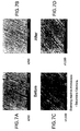
- the surface of a titanium target surface treated by ion etching shows a distinct change in appearance when viewed using a scanning electron microscope as shown in Figures 7A, 7B, 7C and 7D in before and after views.
- Figures 7A, 7B, 7C and 7D machining grooves and deformed material (black spots and tears) have been significantly minimized by practice of the invention.
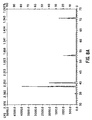
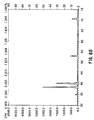
- X-ray diffraction analysis of a machined and chemically etched titanium target shows significant shifts in peak intensities indicating deformed material is being removed by the etching process.
- Diffraction patterns of as machined and etched targets are shown in Figure 8A, 8B, 8C and 8D.
- Figure 8A is the X-ray diffraction pattern of a target surface after machining.
- Figure 8B is the X-ray diffraction pattern of a target surface after a chemical etching treatment for one minute.
- Figure 8C is the X-ray diffraction pattern of a target surface after a chemical etching treatment for five minutes.
- Figure 8D is the X-ray diffraction pattern of a target surface after a chemical etching treatment for ten minutes.
- any type of target can be produced with the invention, including any materials and single piece targets as well as bonded assemblies.
- the targets can be used in any sputtering systems, the invention is not sputtering system dependent.
- the targets are used in planar magnetron sputtering systems.
- the portion of the target to be treated can also vary depending on the sputtering process. Generally, one side of the target is used for sputtering and this side is subjected to the surface treatment. However, depending on the target configuration and use, other portions of the target can be subjected to the surface treatment step.
- the surface treatment step does not impact any of the other critical parameters of the target such as grain size, crystallographic orientation, bulk impurity and gas content and the like.
- the surface treated portion is protected with a metallic enclosure.
- the metallic enclosure separates and isolates the surface treated portion from subsequent exposure and/or contact with possible contaminating material, e.g., plastic packing bags used for storage and shipment, airborne contaminants such as dust or the like, moisture, or any other materials which, when put in contact with the surface treated portion of the target, could adversely affect the sputtering operation.
- an exemplary target assembly is generally designated by the reference numeral 10 and includes the target 1 with the surface treated portion 3 thereon and a metallic enclosure 5 in the shape of a cover or cap.
- the cover 5 has a peripheral lip 7 which, with the cover body 9, encloses the surface treated portion 3 of the target 1.
- FIG. 9 A more detailed depiction of a target and a cover is shown in Figure 9.
- a seal or a spacer 26 can be placed between the target flange 27 and the cover 5 to protect the target from being scratched and further protect the target surface.
- the seal is sized so that the seal surface engages the flange of the target. This engagement may be used as a seal to further isolate and separate the surface treated portion from potential contamination.
- the cover is sized so that an inner wall 11 of the lip 7 encloses the sidewall 13 of the target 1.
- This engagement or seal further isolates and separates the surface treated portion 3 from potential contaminants.
- other types of seals rather than a friction or pressure fit can be used, for example, gaskets, O-rings, removable adhesives, tape or the like.
- the fit between the lip 7 and the target 1 should leave a sufficient gap between the underside 15 of the cap body 9 and the surface treated portion 3 to prevent contact therebetween when the cover is installed and/or removed.
- the fit between the lip 7 and the sidewall 13 must also be designed to prevent scratching of the sidewall 13.
- cover 5 can be used, particularly depending on the target configuration.
- a metallic enclosure comprising two halves which can be attached together could be employed to enclose the entire target.
- the metallic enclosure could be in the shape of a container with a door to access the container inside for target insertion and removal.
- target configuration can be any type known in the art, for example, circular, oval, rectangular, square or any other shape.
- Figure 2 shows an exemplary cross-section of a further packaging, i.e, a double plastic bag assembly 20 comprising a pair of plastic bags 21 and 23.
- the plastic bags 21 and 23 can have closures to permit insertion of the target assembly 10 into the bag 23 followed by insertion of the target assembly-containing bag 23 into the bag 21.
- the cover 5 is preferably metallic.
- the metallic cover prevents contact or exposure between the plastic bag 23 and the surface of the target. Plastic or polymeric materials tend to contaminate the target surface by providing a source of organic material which would be detrimental if present in the sputtering or burn-in process.
- the metallic cover eliminates contact between the target and any plastic and any source of organic radicals and carbon generated during sputtering and/or burn-in.
- any metal having sufficient strength can be used as the metal for the cover or enclosure, e.g., ferrous or nonferrous metals, either in laminate, coated, composite or other known forms.
- the cover can comprise a non-metallic core, e.g. plastic, a composite or the like, and a metal coating thereon. The metal coating can cover the entire non-metallic core or just the portion adjacent the surface treated target portion.
- a metallic enclosure is deemed to encompass any enclosures having at least a metal portion protecting and/or isolating the surface treated target portion.
- the assembly 20 can also include a desiccant 25.
- the purpose of the desiccant is to reduce water vapor that can be adsorbed by the target. Since these desiccants are well known in the art, a further description is not deemed necessary for understanding of the invention.
- the assembly 20 can be evacuated to form the package 30 as shown in Figure 3.
- the package 30 is then ready for transport or storage prior to use of the target for reduced, final burn-in and subsequent sputtering.
- plastic enclosures and desiccant depicted in Figures 2 and 3 are preferred embodiments of the present invention. However, other types of enclosures and/or desiccants can be used to enclose the target assembly 10. For example, a single plastic bag or a shrink-wrap plastic film could be utilized.
- the plastic for use in the bag or film can be a moisture and/or gas resistant type such as polyethylene to provide an additional mode of protection for the target.
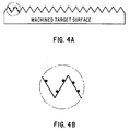
- FIG. 4A A depiction of a typical and conventionally produced target surface profile of a machined target is shown in Figure 4A.
- An enlarged portion of the machine target surface is depicted in 4B.
- Conventional machining can result in one or more defects such as deformed material, smearing, twins, and/or burns on the machined target surface.
- Figures 4A and 4B also show the presence of contaminants on the machine target surface.
- the surface treatment step of the invention removes the defects mentioned above and can also reduce the microscopic surface area of the machined target surface.
- the conventionally machined target surface is made flatter, i.e., the peaks are reduced in size, so that the overall surface area is lessened.
- the surface treatment results in a significant decrease in the generation of particles added during the sputtering process.
- Figure 5 shows the number of particles greater than 0.19 microns in size added per wafer during sputtering operation for 200 mm wafers as measured by a Tencor 6200 tools with a 3mm edge exclusion.
- the performance of the inventive target is compared to that of a prior art target made from the same material with identical metallurgical properties.
- the same apparatus an Applied Materials Endura 5500 sputtering system
- burn-in procedure -10 microns deposited film
- operating conditions were used in testing each type of target.
- the graph depicts the performance of the targets during the first 20 kwh (kilo watt hour) of life after the burn-in.
- the conventionally machined surface produces a significantly increased number of particles added per wafer, with a large wafer to wafer variation as compared to a target surface treated and packaged according to the invention.
- the inventive target was processed by ion etching the sputtering surface of the target. Looking at the surface appearance of the machined and ion etched targets in Figures 7A-7D, it is clearly evident that the inventive target surface treatment removed the contaminants and machined defects dramatically reducing particle generation at beginning of life.
- Another inventive target was processed by chemical etching. Looking at the surface appearance the machined and chemically etched targets in Figures 8A-8D, it is clearly evident with the inventive target surface that all machining grooves and deformed material have been removed to reveal the underlying grain structure. This allowed a reduction of burn-in time from 5-6 hours to less than one hour to achieve a low particulate stable process.
- a thin barrier film can be applied to the surface treated portion of the target for passivation purposes.
- the thin metal film can be any type which will passivate the target surface but can still be removed during the burn-in and/or sputtering and could promote adhesion to "back sputtered" fixtures such as shielding operations.
- a native oxide film will form once a target is manufactured, e.g., TiO 2 on titanium or Al 2 O 3 on aluminum. These oxides should be removed during burn-in but are difficult to sputter and may be present at slower eroding regions of the target for a significant period of the target life.
- the thin metal film can be a precious metal-containing film such as one selected from the platinum group or the gold group. However, any material which will prevent contamination or oxidation of the surface treated target portion can be utilized.
- the manner of applying the passivating barrier film can be any known metallic coating process.
- processes include flame spraying, arc spraying, plasma spraying, laser coating, electrostatic powder coating, slurry coatings, roll bonding, powder rolling, mechanical impingement, explosive bonding, plasma-transferred arc cladding, chemical vapor deposition, thermal decomposition, physical vapor deposition techniques such as evaporation or reactive evaporation, ion plating, sputtering and ion implantation or other similar type processes.
- These processes must be performed in-situ with the cleaning process to prevent the formation of oxides. Since these processes are well known in the art, a further description thereof is not deemed necessary for understanding of the invention.
- Figure 6 shows an exemplary passivated and surface treated target designated by the reference numeral 40.
- the passivation layer 41 is coated on the surface treated portion of the target.
- the target with the passivation layer 41 can then be packaged, stored and shipped as described above.
- the reduction of particles and impurities generated during the burn-in stage may also prolong tool uptime before preventive maintenance/shield kit changes have to be performed.
- the surface treatment method and target assembly is not system dependent. It can be used in any sputtering system, particularly, planar magnetron sputtering systems.
- the inventive method is good for any target materials including aluminum, titanium, transition metals, refractory metals, silicides, indium tin oxide, composites, bonded assemblies or combinations thereof.
- the improvements described above are achieved without any compromise in the end user's process, product specification such as uniformity, deposition rate, particles, etc..
- an invention has been disclosed in terms of preferred embodiments thereof which fulfill each and every one of the objects of the present invention as set forth above and provides a new and improved method for reducing the burn-in time for sputtering targets and an improved target assembly.
Landscapes
- Chemical & Material Sciences (AREA)
- Chemical Kinetics & Catalysis (AREA)
- Engineering & Computer Science (AREA)
- Materials Engineering (AREA)
- Mechanical Engineering (AREA)
- Metallurgy (AREA)
- Organic Chemistry (AREA)
- Physical Vapour Deposition (AREA)
Claims (29)
- Bei einem Verfahren zur Herstellung einer Targetoberfläche vor der Verwendung des Targets zum Sputtern besteht die Verbessern darin, dass vor dem Einbrennen:a) mindestens ein Teil des Targets einem nicht-mechanischen Oberflächenbehandlungsschritt unterworfen wird, um einen oberflächenbehandelten Targetbereich zu erzeugen und durch welchen mindestens eine auf dem oberflächenbehandelten Targetbereich vorhandene Verunreinigung entfernt wird und die Oberfläche des oberflächenbehandelten Targetbereichs verringert wird; undb) mindestens der oberflächenbehandelte Targetbereich des Targets in einer metallischen Umhüllung angeordnet wird, die so bemessen ist, dass sie mindestens den oberflächenbehandelten Targetbereich umschließt, wobei die metallische Umhüllung einen Kontakt zwischen dem oberflächenbehandelten Targetbereich des Targets und einer nachfolgend verwendeten Kunststoffumhüllung, welche die metallische Umhüllung umschließt, verhindert;c) wobei der nicht mechanische Oberflächenbehandlungsschritt und die metallische Umhüllung das Einbrennen vermindern.
- Verfahren nach Anspruch 1, bei welchem die metallische Umhüllung und das Target in einer Kunststoffumhüllung eingeschlossen werden.
- Verfahren gemäß Anspruch 2, bei welchem die Kunststoffumhüllung evakuiert wird.
- Verfahren gemäß Anspruch 2, bei welchem ein Trocknungsmittel in die Kunststoffumhüllung eingebracht wird.
- Verfahren gemäß Anspruch 4, bei welchem die Kunststoffumhüllung evakuiert wird.
- Verfahren gemäß Anspruch 1, bei welchem der nicht mechanische Oberflächenbehandlungsschritt eine Oberflächenbehandlung des Bereichs des Targets mittels einem der nachstehenden Verfahren umfaßt: ionischem Reinigen, ionischem Zerkleinern, chemischem Ätzen, Sputtern, chemischem Polieren, elektrolytischem Polieren, elektrolytischem Ätzen, Laserablation, Elektronenstrahlablation oder Kombinationen derselben.
- Verfahren gemäß Anspruch 6, bei welchem der nicht mechanische Oberflächenbehandlungsschritt eine ionische Reinigung umfaßt.
- Verfahren gemäß Anspruch 1, bei welchem die metallische Umhüllung aus einem nicht metallischem Kern mit einem Metallüberzug gefertigt ist.
- Verfahren gemäß Anspruch 1, bei welchem die metallische Umhüllung eine Abdeckung mit mindestens einem metallischen Bereich ist, der bemessen ist, um an dem Target so angebracht zu werden, dass mindestens der metallische Bereich der Abdeckung mindestens den oberflächenbehandelten Bereich des Targets umschließt.
- Verfahren gemäß Anspruch 5, bei welchem der nicht mechanische Oberflächenbehandlungsschritt eine Oberflächenbehandlung des Bereichs des Targets durch eines der nachstehenden Verfahren umfaßt: ionischem Reinigen, ionischem Zerkleinern, Sputtern, chemischem Ätzen, chemischem Polieren, elektrolytischem Polieren, elektrolytischem Ätzen, Laserablation, Elektronenstrahlablation oder Kombinationen derselben.
- Verfahren gemäß Anspruch 10, bei welchem der nicht mechanische Oberflächenbehandlungsschritt ionisches Reinigen umfaßt.
- Verfahren gemäß Anspruch 1, bei welchem ein Passivierungsüberzug auf mindestens den oberflächebehandelten Targetbereich des Targets aufgebracht wird.
- Verfahren gemäß Anspruch 12, bei welchem der Passivierungsüberzug eine aufgebrachte Lage eines Edelmetalls oder eines anderen nicht oxidierenden Materials ist.
- Verfahren gemäß Anspruch 9, bei welchem die Abdeckung eine Lippe aufweist, die mit einem peripheren Rand des Targets in Eingriff tritt.
- Verfahren gemäß Anspruch 14, bei welchem die Abdeckung eine Metallkappe umfaßt.
- Verfahren gemäß Anspruch 1, bei welchem der nicht mechanische Oberflächenbehandlungsschritt wirksam ist, um deformiertes Material, Verschmierungen, Zwillingsbildungen oder Grate, die auf der Oberfläche vorhanden sind, zu entfernen.
- Targetbaugruppe zum Verringern der Einbrenndauer eines Targets vor dem Targetsputtern, versehen mit:a) einem Sputtertarget mit mindestens einem oberflächenbehandelten Bereich, der nicht mechanisch oberflächenbehandelt ist, so dass mindestens eine der Verunreinigungen an dem oberflächenbehandelten Bereich entfernt wurde und die Oberfläche des oberflächenbehandelten Bereichs verringert ist; undb) einer metallischen Umhüllung, die so bemessen ist, dass sie mindestens den oberflächenbehandelten Bereich des Sputtertargets umschließ, so dass mindestens der oberflächenbehandelte Bereich des Sputtertargets von einer Verpackungsumhüllung getrennt ist, die nachfolgend verwendet wird, um die metallische Umhüllung und das Sputtertarget zu umschließen, und wodurch die Einbrenndauer verringert wird.
- Targetbaugruppe gemäß Anspruch 17, bei welcher die Verpackungsumhüllung eine Kunststoffumhüllung aufweist, welche die metallische Umhüllung und das Target umgibt.
- Targetbaugruppe gemäß Anspruch 17, bei welcher die Verpackungsumhüllung eine die metallische Umhüllung und das Target umgebende Kunststoffvakuumumhüllung aufweist.
- Targetbaugruppe gemäß Anspruch 19, bei welcher die Kunststoffvakuumumhüllung eine Doppeltasche ist.
- Targetbaugruppe gemäß Anspruch 18, versehen mit einem Trocknungsmittel im Innern der Kunststoffumhüllung.
- Targetbaugruppe gemäß Anspruch 17, bei welcher die metallische Umhüllung eine Abdeckung mit mindestens einem metallischen Bereich ist, der bemessen ist, um so an dem Target angebracht zu werden, dass mindestens der metallische Bereich der Abdeckung mindestens den oberflächenbehandelten Bereich umschließt.
- Targetbaugruppe gemäß Anspruch 22, bei welcher die Verpackungsumhüllung eine Kunststoffumhüllung aufweist, welche die Abdeckung und das Target umgibt.
- Targetbaugruppe gemäß Anspruch 23, bei welcher die Kunststoffumhüllung eine Vakuumdoppeltasche mit einem darin befindlichen Trocknungsmittel ist.
- Targetbaugruppe gemäß Anspruch 17, bei welcher die metallische Umhüllung eine Abdeckung mit mindestens einem metallischen Bereich und einer peripheren Lippe ist, wobei die Abdeckung so bemessen ist, dass die periphere Lippe mit einem peripheren Rand des Targets so in Eingriff tritt, dass mindestens der metallische Bereich der Abdeckung mindestens den oberflächenbehandelten Bereich umschließt.
- Targetbaugruppe gemäß Anspruch 25, bei welcher die Abdeckung eine Metallkappe ist.
- Targetbaugruppe gemäß Anspruch 17, bei welcher auf dem oberflächenbehandelten Bereich eine Sperrschicht vorgesehen ist.
- Targetbaugruppe gemäß Anspruch 27, bei welcher die Sperrschicht ein Edelmetall oder ein anderes nicht oxidierendes Material aufweist.
- Targetbaugruppe gemäß Anspruch 17, bei welcher der oberflächenbehandelte Bereich im wesentlichen frei von deformiertem Material, Verschmierungen, Zwillingsbildungen oder Graten ist.
Applications Claiming Priority (3)
| Application Number | Priority Date | Filing Date | Title |
|---|---|---|---|
| US08/850,707 US6030514A (en) | 1997-05-02 | 1997-05-02 | Method of reducing sputtering burn-in time, minimizing sputtered particulate, and target assembly therefor |
| US850707 | 1997-05-02 | ||
| PCT/US1998/008961 WO1998050598A1 (en) | 1997-05-02 | 1998-05-04 | Method of reducing sputtering burn-in time, minimizing sputtered particulate, and target assembly therefor |
Publications (3)
| Publication Number | Publication Date |
|---|---|
| EP0977905A1 EP0977905A1 (de) | 2000-02-09 |
| EP0977905A4 EP0977905A4 (de) | 2002-11-20 |
| EP0977905B1 true EP0977905B1 (de) | 2006-02-08 |
Family
ID=25308900
Family Applications (1)
| Application Number | Title | Priority Date | Filing Date |
|---|---|---|---|
| EP98918931A Expired - Lifetime EP0977905B1 (de) | 1997-05-02 | 1998-05-04 | Verfahren zur reduzierung der einbrennzeit eines sputters, minimierung der sputterpartikel und targetvorrichtung dafür |
Country Status (8)
| Country | Link |
|---|---|
| US (1) | US6030514A (de) |
| EP (1) | EP0977905B1 (de) |
| JP (2) | JP2002511115A (de) |
| AT (1) | ATE317460T1 (de) |
| AU (1) | AU7175298A (de) |
| CA (1) | CA2288987A1 (de) |
| DE (1) | DE69833432T2 (de) |
| WO (1) | WO1998050598A1 (de) |
Families Citing this family (46)
| Publication number | Priority date | Publication date | Assignee | Title |
|---|---|---|---|---|
| JP3576364B2 (ja) * | 1997-10-13 | 2004-10-13 | 株式会社日鉱マテリアルズ | Itoスパッタリングターゲットのクリーニング方法 |
| US6309556B1 (en) * | 1998-09-03 | 2001-10-30 | Praxair S.T. Technology, Inc. | Method of manufacturing enhanced finish sputtering targets |
| EP1135233A4 (de) | 1998-12-03 | 2004-11-03 | Tosoh Smd Inc | Treffplatte und verfahren zu seiner herstellung |
| US6283357B1 (en) * | 1999-08-03 | 2001-09-04 | Praxair S.T. Technology, Inc. | Fabrication of clad hollow cathode magnetron sputter targets |
| US6495966B2 (en) * | 1999-09-08 | 2002-12-17 | Matsushita Electric Industrial Co., Ltd. | Field emission display including a resistor |
| US6428663B1 (en) * | 2000-07-03 | 2002-08-06 | Applied Materials, Inc. | Preventing defect generation from targets through applying metal spray coatings on sidewalls |
| JP4642255B2 (ja) * | 2000-09-04 | 2011-03-02 | Jx日鉱日石金属株式会社 | 酸化変色防止剤を施した銅又は銅合金製スパッタリングターゲットおよびその処理法 |
| TW512180B (en) * | 2000-09-21 | 2002-12-01 | Promos Technologies Inc | Method for maintaining the cleanness of a vacuum chamber of physical vapor deposition system |
| DE60139406D1 (de) * | 2000-11-17 | 2009-09-10 | Nippon Mining Co | Sputtering-target, das wenig partikel produziert, belagträgerplatte mit dem target und verfahren zur herstellung des targets |
| US6887356B2 (en) * | 2000-11-27 | 2005-05-03 | Cabot Corporation | Hollow cathode target and methods of making same |
| JP4495855B2 (ja) * | 2000-12-11 | 2010-07-07 | 株式会社東芝 | チタンスパッタリングターゲットおよびその製造方法 |
| US20020170897A1 (en) * | 2001-05-21 | 2002-11-21 | Hall Frank L. | Methods for preparing ball grid array substrates via use of a laser |
| CN1289709C (zh) * | 2001-08-13 | 2006-12-13 | 贝卡尔特股份有限公司 | 用于制造溅射靶的方法 |
| JP5051954B2 (ja) * | 2001-09-17 | 2012-10-17 | エルエスアイ コーポレーション | スパツタリング方法及び該方法に使用するスパツタリングターゲット用カバー |
| JP2003293126A (ja) * | 2002-04-09 | 2003-10-15 | Fujitsu Ltd | スパッタリングターゲット及びその製造方法 |
| US6977800B2 (en) * | 2003-07-29 | 2005-12-20 | Hitachi Global Storage Technologies Netherlands B.V. | Magnetic read head with dual layer lead |
| US20050040030A1 (en) * | 2003-08-20 | 2005-02-24 | Mcdonald Peter H. | Method of treating sputtering target to reduce burn-in time and sputtering target thereof and apparatus thereof |
| US20050072668A1 (en) * | 2003-10-06 | 2005-04-07 | Heraeus, Inc. | Sputter target having modified surface texture |
| US20050236270A1 (en) * | 2004-04-23 | 2005-10-27 | Heraeus, Inc. | Controlled cooling of sputter targets |
| US8030082B2 (en) * | 2006-01-13 | 2011-10-04 | Honeywell International Inc. | Liquid-particle analysis of metal materials |
| US20070215463A1 (en) * | 2006-03-14 | 2007-09-20 | Applied Materials, Inc. | Pre-conditioning a sputtering target prior to sputtering |
| US20080110746A1 (en) * | 2006-11-09 | 2008-05-15 | Kardokus Janine K | Novel manufacturing design and processing methods and apparatus for sputtering targets |
| US20080121516A1 (en) * | 2006-11-29 | 2008-05-29 | Jaydeep Sarkar | Method and apparatus for treating sputtering target to reduce burn-in time and sputtering targets made thereby |
| JP5215192B2 (ja) * | 2007-01-05 | 2013-06-19 | 株式会社東芝 | スパッタリングターゲット |
| WO2008127493A1 (en) * | 2007-01-29 | 2008-10-23 | Tosoh Smd, Inc. | Ultra smooth face sputter targets and methods of producing same |
| TWI432592B (zh) * | 2007-04-27 | 2014-04-01 | Honeywell Int Inc | 具有降低預燒時間之濺鍍靶,其製造方法及其用途 |
| JP4833942B2 (ja) | 2007-08-29 | 2011-12-07 | 株式会社コベルコ科研 | Ag基合金スパッタリングターゲット |
| US8968528B2 (en) * | 2008-04-14 | 2015-03-03 | United Technologies Corporation | Platinum-modified cathodic arc coating |
| JP5032662B2 (ja) * | 2008-10-29 | 2012-09-26 | Jx日鉱日石金属株式会社 | 希土類金属又はこれらの酸化物からなるターゲットの保管方法 |
| WO2010101051A1 (ja) * | 2009-03-03 | 2010-09-10 | 日鉱金属株式会社 | スパッタリングターゲット及びその製造方法 |
| KR101975741B1 (ko) * | 2009-11-13 | 2019-05-09 | 가부시키가이샤 한도오따이 에네루기 켄큐쇼 | 타깃 재료의 포장 방법 및 타깃의 장착 방법 |
| EP2503020B1 (de) | 2009-11-17 | 2014-11-26 | JX Nippon Mining & Metals Corporation | Verfahren zur lagerung eines lanthanoxid-targets und vakuumverpacktes lanthanoxid-target |
| US8449817B2 (en) * | 2010-06-30 | 2013-05-28 | H.C. Stark, Inc. | Molybdenum-containing targets comprising three metal elements |
| JP4948634B2 (ja) | 2010-09-01 | 2012-06-06 | Jx日鉱日石金属株式会社 | インジウムターゲット及びその製造方法 |
| EP2699708B1 (de) * | 2011-04-21 | 2018-11-14 | View, Inc. | Lithium-sputtertarget |
| WO2013003065A2 (en) | 2011-06-30 | 2013-01-03 | Soladigm, Inc. | Sputter target and sputtering methods |
| WO2013070679A1 (en) | 2011-11-08 | 2013-05-16 | Tosoh Smd, Inc. | Silicon sputtering target with special surface treatment and good particle performance and methods of making the same |
| JP5074628B1 (ja) * | 2012-01-05 | 2012-11-14 | Jx日鉱日石金属株式会社 | インジウム製スパッタリングターゲット及びその製造方法 |
| EP2818575B1 (de) | 2012-08-22 | 2018-05-30 | JX Nippon Mining & Metals Corp. | Zylinderförmiges indiumsputtertarget und verfahren zur herstellung davon |
| WO2015004958A1 (ja) | 2013-07-08 | 2015-01-15 | Jx日鉱日石金属株式会社 | スパッタリングターゲット及び、それの製造方法 |
| WO2016180452A1 (en) * | 2015-05-08 | 2016-11-17 | Applied Materials, Inc. | Protection tube for reactive targets |
| CN107771115B (zh) | 2015-05-15 | 2021-10-22 | 美题隆公司 | 溅射靶的表面处理方法 |
| JP6138307B2 (ja) * | 2016-03-09 | 2017-05-31 | Jx金属株式会社 | スパッタリングターゲット及びその製造方法 |
| US10570504B2 (en) * | 2017-04-26 | 2020-02-25 | International Business Machines Corporation | Structure and method to fabricate highly reactive physical vapor deposition target |
| US11139151B1 (en) * | 2018-03-15 | 2021-10-05 | Intel Corporation | Micro-surface morphological matching for reactor components |
| JP6885981B2 (ja) | 2019-03-29 | 2021-06-16 | Jx金属株式会社 | スパッタリングターゲットの梱包物の作製方法及び輸送方法 |
Family Cites Families (26)
| Publication number | Priority date | Publication date | Assignee | Title |
|---|---|---|---|---|
| US3827472A (en) * | 1969-12-05 | 1974-08-06 | Seisan Nipponsha Kk | Reclosable bag |
| US4450062A (en) * | 1981-12-22 | 1984-05-22 | Raytheon Company | Sputtering apparatus and methods |
| JPS6066425A (ja) * | 1983-09-22 | 1985-04-16 | Nippon Telegr & Teleph Corp <Ntt> | Lsi電極用の高純度モリブデンタ−ゲツトならびに高純度モリブデンシリサイドタ−ゲツトおよびその製造方法 |
| DD252005A1 (de) * | 1986-08-12 | 1987-12-02 | Ardenne Forschungsinst | Verfahren zur vorbehandlung von aluminiumtargets zum hochratezerstaeuben |
| DE3631830A1 (de) * | 1986-09-19 | 1988-03-31 | Demetron | Mehrstofflegierung fuer targets von kathodenzerstaeubungsanlagen und deren verwendung |
| IT209910Z2 (it) * | 1987-02-06 | 1988-11-04 | Sgs Microelettronica Spa | Contenitore porta-wafer o fretta di slicio, utilizzato perl'immagazzinamento e/o spedizione sotto vuoto degli stessi. |
| US5035787A (en) * | 1987-07-22 | 1991-07-30 | Microbeam, Inc. | Method for repairing semiconductor masks and reticles |
| KR920003789B1 (ko) * | 1988-02-08 | 1992-05-14 | 니뽄 덴신 덴와 가부시끼가이샤 | 플라즈마 스퍼터링을 이용한 박막 형성 장치 및 이온원 |
| DE3819906C1 (de) * | 1988-06-11 | 1989-08-03 | Degussa Ag, 6000 Frankfurt, De | |
| JPH02159372A (ja) * | 1988-12-12 | 1990-06-19 | Nec Corp | スパッタリングターゲット用保護容器 |
| JPH03257158A (ja) * | 1990-03-07 | 1991-11-15 | Toshiba Corp | スパッタリングターゲット |
| JP2864687B2 (ja) * | 1990-07-30 | 1999-03-03 | 三菱瓦斯化学株式会社 | 二重包装体及びその包装方法 |
| US5104684A (en) * | 1990-05-25 | 1992-04-14 | Massachusetts Institute Of Technology | Ion beam induced deposition of metals |
| WO1992004482A1 (en) * | 1990-08-30 | 1992-03-19 | Materials Research Corporation | Pretextured cathode sputtering target and method of preparation thereof and sputtering therewith |
| JPH04231461A (ja) * | 1990-12-27 | 1992-08-20 | Tosoh Corp | スパッタリングターゲットの保護具及び包装方法 |
| JPH04297560A (ja) * | 1991-03-26 | 1992-10-21 | Nisshin Steel Co Ltd | 鋼帯の連続溶融めっき方法及び装置 |
| JPH04304367A (ja) * | 1991-03-29 | 1992-10-27 | Sony Corp | 薄膜形成方法 |
| JPH05125526A (ja) * | 1991-11-08 | 1993-05-21 | Vacuum Metallurgical Co Ltd | スパツタリング用ターゲツト |
| FR2697000B1 (fr) * | 1992-10-16 | 1994-11-25 | Commissariat Energie Atomique | Boîte plate de confinement d'un objet plat sous atmosphère spéciale. |
| US5324448A (en) * | 1992-12-14 | 1994-06-28 | A + Corp. | Combination dessicant and vapor-corrosion inhibitor |
| JPH06306590A (ja) * | 1993-04-28 | 1994-11-01 | Sony Corp | スパッタリング装置用金属ターゲット |
| EP0634498A1 (de) * | 1993-07-16 | 1995-01-18 | Applied Materials, Inc. | Angeätzter Zerstäubungs-Target und Verfahren |
| US5358615A (en) * | 1993-10-04 | 1994-10-25 | Motorola, Inc. | Process for forming a sputter deposited metal film |
| US5529671A (en) * | 1994-07-27 | 1996-06-25 | Litton Systems, Inc. | Apparatus and method for ion beam polishing and for in-situ ellipsometric deposition of ion beam films |
| JPH08246145A (ja) * | 1995-03-13 | 1996-09-24 | Vacuum Metallurgical Co Ltd | 誘電体ターゲットの保管容器および保管方法 |
| JPH09143707A (ja) * | 1995-11-29 | 1997-06-03 | Hitachi Metals Ltd | スパッタリング用ターゲットの製造方法およびスパッタリング用ターゲット |
-
1997
- 1997-05-02 US US08/850,707 patent/US6030514A/en not_active Expired - Lifetime
-
1998
- 1998-05-04 CA CA002288987A patent/CA2288987A1/en not_active Abandoned
- 1998-05-04 WO PCT/US1998/008961 patent/WO1998050598A1/en not_active Ceased
- 1998-05-04 DE DE69833432T patent/DE69833432T2/de not_active Expired - Fee Related
- 1998-05-04 JP JP54829098A patent/JP2002511115A/ja not_active Ceased
- 1998-05-04 AT AT98918931T patent/ATE317460T1/de not_active IP Right Cessation
- 1998-05-04 EP EP98918931A patent/EP0977905B1/de not_active Expired - Lifetime
- 1998-05-04 AU AU71752/98A patent/AU7175298A/en not_active Abandoned
-
2010
- 2010-04-26 JP JP2010100806A patent/JP5037649B2/ja not_active Expired - Lifetime
Also Published As
| Publication number | Publication date |
|---|---|
| DE69833432T2 (de) | 2006-09-28 |
| EP0977905A1 (de) | 2000-02-09 |
| AU7175298A (en) | 1998-11-27 |
| JP5037649B2 (ja) | 2012-10-03 |
| ATE317460T1 (de) | 2006-02-15 |
| WO1998050598A1 (en) | 1998-11-12 |
| EP0977905A4 (de) | 2002-11-20 |
| JP2002511115A (ja) | 2002-04-09 |
| DE69833432D1 (de) | 2006-04-20 |
| CA2288987A1 (en) | 1998-11-12 |
| US6030514A (en) | 2000-02-29 |
| JP2010189768A (ja) | 2010-09-02 |
Similar Documents
| Publication | Publication Date | Title |
|---|---|---|
| US6030514A (en) | Method of reducing sputtering burn-in time, minimizing sputtered particulate, and target assembly therefor | |
| US8147664B2 (en) | Sputtering apparatus | |
| JP5554465B2 (ja) | パーティクルの発生を削減するためのプロセスキットの設計 | |
| KR101355303B1 (ko) | 전자 디바이스의 제조 방법 및 스퍼터링 방법 | |
| US6126791A (en) | Target for use in magnetron sputtering of aluminum for forming metallization films having low defect densities and methods for manufacturing and using such target | |
| EP1178133A2 (de) | Verfahren zur Verlängerung der Lebensdauer von einem wiederverwertbaren Teil zur Verfahrensdurchführung | |
| TW380278B (en) | Back sputtering shield | |
| US20230143320A1 (en) | Sputter trap having a thin high purity coating layer and method of making the same | |
| US7150810B2 (en) | Sputtering target and method for fabricating the same | |
| WO2016099804A1 (en) | Particle reduction in a deposition chamber using thermal expansion coefficient compatible coating | |
| JP2010275574A (ja) | スパッタリング装置および半導体装置製造方法 | |
| KR100591433B1 (ko) | 질화 티타늄(TiN) 스퍼터링 공정용 실드 및 코팅방법 | |
| US20050040030A1 (en) | Method of treating sputtering target to reduce burn-in time and sputtering target thereof and apparatus thereof | |
| US20020104756A1 (en) | Sputtering apparatus | |
| US5240580A (en) | Conmag shield | |
| JPH02285067A (ja) | 真空薄膜形成装置 | |
| JP5051954B2 (ja) | スパツタリング方法及び該方法に使用するスパツタリングターゲット用カバー | |
| KR20240002931A (ko) | 집진 방법 | |
| JPS59208071A (ja) | 成膜方法および装置 | |
| JPS63121659A (ja) | スパツタリング装置 | |
| US20080121516A1 (en) | Method and apparatus for treating sputtering target to reduce burn-in time and sputtering targets made thereby | |
| JPS6026659A (ja) | スパツタリング装置 | |
| JPS60135571A (ja) | スパツタリングにおけるタ−ゲツト取付方法 | |
| JP2768980B2 (ja) | 半導体装置の製造方法 | |
| JPH01175738A (ja) | ドライエッチング装置 |
Legal Events
| Date | Code | Title | Description |
|---|---|---|---|
| PUAI | Public reference made under article 153(3) epc to a published international application that has entered the european phase |
Free format text: ORIGINAL CODE: 0009012 |
|
| 17P | Request for examination filed |
Effective date: 19991011 |
|
| AK | Designated contracting states |
Kind code of ref document: A1 Designated state(s): AT BE CH CY DE DK ES FI FR GB GR IE IT LI LU MC NL PT SE |
|
| RIN1 | Information on inventor provided before grant (corrected) |
Inventor name: SCHITTNY, STEPHAN Inventor name: SHIM, CARI Inventor name: FELDEWERTH, GERALD, B. Inventor name: GOLDSTEIN, MICHAEL Inventor name: DUNLOP, JOHN, A. |
|
| A4 | Supplementary search report drawn up and despatched |
Effective date: 20021004 |
|
| AK | Designated contracting states |
Kind code of ref document: A4 Designated state(s): AT BE CH CY DE DK ES FI FR GB GR IE IT LI LU MC NL PT SE |
|
| 17Q | First examination report despatched |
Effective date: 20041215 |
|
| RAP1 | Party data changed (applicant data changed or rights of an application transferred) |
Owner name: PRAXAIR S.T. TECHNOLOGY, INC. Owner name: INTEL CORPORATION |
|
| GRAP | Despatch of communication of intention to grant a patent |
Free format text: ORIGINAL CODE: EPIDOSNIGR1 |
|
| GRAS | Grant fee paid |
Free format text: ORIGINAL CODE: EPIDOSNIGR3 |
|
| GRAA | (expected) grant |
Free format text: ORIGINAL CODE: 0009210 |
|
| AK | Designated contracting states |
Kind code of ref document: B1 Designated state(s): AT BE CH CY DE DK ES FI FR GB GR IE IT LI LU MC NL PT SE |
|
| PG25 | Lapsed in a contracting state [announced via postgrant information from national office to epo] |
Ref country code: NL Free format text: LAPSE BECAUSE OF FAILURE TO SUBMIT A TRANSLATION OF THE DESCRIPTION OR TO PAY THE FEE WITHIN THE PRESCRIBED TIME-LIMIT Effective date: 20060208 Ref country code: LI Free format text: LAPSE BECAUSE OF FAILURE TO SUBMIT A TRANSLATION OF THE DESCRIPTION OR TO PAY THE FEE WITHIN THE PRESCRIBED TIME-LIMIT Effective date: 20060208 Ref country code: FI Free format text: LAPSE BECAUSE OF FAILURE TO SUBMIT A TRANSLATION OF THE DESCRIPTION OR TO PAY THE FEE WITHIN THE PRESCRIBED TIME-LIMIT Effective date: 20060208 Ref country code: CH Free format text: LAPSE BECAUSE OF FAILURE TO SUBMIT A TRANSLATION OF THE DESCRIPTION OR TO PAY THE FEE WITHIN THE PRESCRIBED TIME-LIMIT Effective date: 20060208 Ref country code: BE Free format text: LAPSE BECAUSE OF FAILURE TO SUBMIT A TRANSLATION OF THE DESCRIPTION OR TO PAY THE FEE WITHIN THE PRESCRIBED TIME-LIMIT Effective date: 20060208 Ref country code: AT Free format text: LAPSE BECAUSE OF FAILURE TO SUBMIT A TRANSLATION OF THE DESCRIPTION OR TO PAY THE FEE WITHIN THE PRESCRIBED TIME-LIMIT Effective date: 20060208 |
|
| REG | Reference to a national code |
Ref country code: GB Ref legal event code: FG4D |
|
| REG | Reference to a national code |
Ref country code: CH Ref legal event code: EP |
|
| REG | Reference to a national code |
Ref country code: IE Ref legal event code: FG4D |
|
| REF | Corresponds to: |
Ref document number: 69833432 Country of ref document: DE Date of ref document: 20060420 Kind code of ref document: P |
|
| PG25 | Lapsed in a contracting state [announced via postgrant information from national office to epo] |
Ref country code: IE Free format text: LAPSE BECAUSE OF NON-PAYMENT OF DUE FEES Effective date: 20060504 |
|
| PG25 | Lapsed in a contracting state [announced via postgrant information from national office to epo] |
Ref country code: SE Free format text: LAPSE BECAUSE OF FAILURE TO SUBMIT A TRANSLATION OF THE DESCRIPTION OR TO PAY THE FEE WITHIN THE PRESCRIBED TIME-LIMIT Effective date: 20060508 Ref country code: GB Free format text: LAPSE BECAUSE OF NON-PAYMENT OF DUE FEES Effective date: 20060508 Ref country code: DK Free format text: LAPSE BECAUSE OF FAILURE TO SUBMIT A TRANSLATION OF THE DESCRIPTION OR TO PAY THE FEE WITHIN THE PRESCRIBED TIME-LIMIT Effective date: 20060508 |
|
| PG25 | Lapsed in a contracting state [announced via postgrant information from national office to epo] |
Ref country code: ES Free format text: LAPSE BECAUSE OF FAILURE TO SUBMIT A TRANSLATION OF THE DESCRIPTION OR TO PAY THE FEE WITHIN THE PRESCRIBED TIME-LIMIT Effective date: 20060519 |
|
| PG25 | Lapsed in a contracting state [announced via postgrant information from national office to epo] |
Ref country code: MC Free format text: LAPSE BECAUSE OF NON-PAYMENT OF DUE FEES Effective date: 20060531 |
|
| PGFP | Annual fee paid to national office [announced via postgrant information from national office to epo] |
Ref country code: IT Payment date: 20060531 Year of fee payment: 9 |
|
| NLV1 | Nl: lapsed or annulled due to failure to fulfill the requirements of art. 29p and 29m of the patents act | ||
| PG25 | Lapsed in a contracting state [announced via postgrant information from national office to epo] |
Ref country code: PT Free format text: LAPSE BECAUSE OF FAILURE TO SUBMIT A TRANSLATION OF THE DESCRIPTION OR TO PAY THE FEE WITHIN THE PRESCRIBED TIME-LIMIT Effective date: 20060710 |
|
| REG | Reference to a national code |
Ref country code: CH Ref legal event code: PL |
|
| ET | Fr: translation filed | ||
| PG25 | Lapsed in a contracting state [announced via postgrant information from national office to epo] |
Ref country code: DE Free format text: LAPSE BECAUSE OF NON-PAYMENT OF DUE FEES Effective date: 20061201 |
|
| PLBE | No opposition filed within time limit |
Free format text: ORIGINAL CODE: 0009261 |
|
| STAA | Information on the status of an ep patent application or granted ep patent |
Free format text: STATUS: NO OPPOSITION FILED WITHIN TIME LIMIT |
|
| 26N | No opposition filed |
Effective date: 20061109 |
|
| GBPC | Gb: european patent ceased through non-payment of renewal fee |
Effective date: 20060508 |
|
| REG | Reference to a national code |
Ref country code: FR Ref legal event code: ST Effective date: 20070131 |
|
| PG25 | Lapsed in a contracting state [announced via postgrant information from national office to epo] |
Ref country code: GR Free format text: LAPSE BECAUSE OF FAILURE TO SUBMIT A TRANSLATION OF THE DESCRIPTION OR TO PAY THE FEE WITHIN THE PRESCRIBED TIME-LIMIT Effective date: 20060509 Ref country code: FR Free format text: LAPSE BECAUSE OF NON-PAYMENT OF DUE FEES Effective date: 20060531 |
|
| PG25 | Lapsed in a contracting state [announced via postgrant information from national office to epo] |
Ref country code: LU Free format text: LAPSE BECAUSE OF NON-PAYMENT OF DUE FEES Effective date: 20060504 |
|
| PG25 | Lapsed in a contracting state [announced via postgrant information from national office to epo] |
Ref country code: CY Free format text: LAPSE BECAUSE OF FAILURE TO SUBMIT A TRANSLATION OF THE DESCRIPTION OR TO PAY THE FEE WITHIN THE PRESCRIBED TIME-LIMIT Effective date: 20060208 |
|
| PG25 | Lapsed in a contracting state [announced via postgrant information from national office to epo] |
Ref country code: IT Free format text: LAPSE BECAUSE OF NON-PAYMENT OF DUE FEES Effective date: 20070504 |