EP0970774B1 - Formstempel zum Austragen von flüssigem Lot - Google Patents
Formstempel zum Austragen von flüssigem Lot Download PDFInfo
- Publication number
- EP0970774B1 EP0970774B1 EP99113056A EP99113056A EP0970774B1 EP 0970774 B1 EP0970774 B1 EP 0970774B1 EP 99113056 A EP99113056 A EP 99113056A EP 99113056 A EP99113056 A EP 99113056A EP 0970774 B1 EP0970774 B1 EP 0970774B1
- Authority
- EP
- European Patent Office
- Prior art keywords
- solder
- molding die
- substrate
- die
- cavity
- Prior art date
- Legal status (The legal status is an assumption and is not a legal conclusion. Google has not performed a legal analysis and makes no representation as to the accuracy of the status listed.)
- Expired - Lifetime
Links
Images

Classifications
-
- H—ELECTRICITY
- H10—SEMICONDUCTOR DEVICES; ELECTRIC SOLID-STATE DEVICES NOT OTHERWISE PROVIDED FOR
- H10P—GENERIC PROCESSES OR APPARATUS FOR THE MANUFACTURE OR TREATMENT OF DEVICES COVERED BY CLASS H10
- H10P14/00—Formation of materials, e.g. in the shape of layers or pillars
- H10P14/40—Formation of materials, e.g. in the shape of layers or pillars of conductive or resistive materials
- H10P14/46—Formation of materials, e.g. in the shape of layers or pillars of conductive or resistive materials using a liquid
-
- B—PERFORMING OPERATIONS; TRANSPORTING
- B23—MACHINE TOOLS; METAL-WORKING NOT OTHERWISE PROVIDED FOR
- B23K—SOLDERING OR UNSOLDERING; WELDING; CLADDING OR PLATING BY SOLDERING OR WELDING; CUTTING BY APPLYING HEAT LOCALLY, e.g. FLAME CUTTING; WORKING BY LASER BEAM
- B23K3/00—Tools, devices or special appurtenances for soldering, e.g. brazing, or unsoldering, not specially adapted for particular methods
- B23K3/06—Solder feeding devices; Solder melting pans
- B23K3/0607—Solder feeding devices
-
- B—PERFORMING OPERATIONS; TRANSPORTING
- B23—MACHINE TOOLS; METAL-WORKING NOT OTHERWISE PROVIDED FOR
- B23K—SOLDERING OR UNSOLDERING; WELDING; CLADDING OR PLATING BY SOLDERING OR WELDING; CUTTING BY APPLYING HEAT LOCALLY, e.g. FLAME CUTTING; WORKING BY LASER BEAM
- B23K3/00—Tools, devices or special appurtenances for soldering, e.g. brazing, or unsoldering, not specially adapted for particular methods
- B23K3/06—Solder feeding devices; Solder melting pans
- B23K3/0607—Solder feeding devices
- B23K3/0615—Solder feeding devices forming part of a soldering iron
-
- H—ELECTRICITY
- H10—SEMICONDUCTOR DEVICES; ELECTRIC SOLID-STATE DEVICES NOT OTHERWISE PROVIDED FOR
- H10W—GENERIC PACKAGES, INTERCONNECTIONS, CONNECTORS OR OTHER CONSTRUCTIONAL DETAILS OF DEVICES COVERED BY CLASS H10
- H10W72/00—Interconnections or connectors in packages
- H10W72/01—Manufacture or treatment
- H10W72/011—Apparatus therefor
- H10W72/0113—Apparatus for manufacturing die-attach connectors
-
- H—ELECTRICITY
- H10—SEMICONDUCTOR DEVICES; ELECTRIC SOLID-STATE DEVICES NOT OTHERWISE PROVIDED FOR
- H10W—GENERIC PACKAGES, INTERCONNECTIONS, CONNECTORS OR OTHER CONSTRUCTIONAL DETAILS OF DEVICES COVERED BY CLASS H10
- H10W72/00—Interconnections or connectors in packages
- H10W72/01—Manufacture or treatment
- H10W72/013—Manufacture or treatment of die-attach connectors
-
- B—PERFORMING OPERATIONS; TRANSPORTING
- B23—MACHINE TOOLS; METAL-WORKING NOT OTHERWISE PROVIDED FOR
- B23K—SOLDERING OR UNSOLDERING; WELDING; CLADDING OR PLATING BY SOLDERING OR WELDING; CUTTING BY APPLYING HEAT LOCALLY, e.g. FLAME CUTTING; WORKING BY LASER BEAM
- B23K2101/00—Articles made by soldering, welding or cutting
- B23K2101/36—Electric or electronic devices
- B23K2101/40—Semiconductor devices
-
- H—ELECTRICITY
- H10—SEMICONDUCTOR DEVICES; ELECTRIC SOLID-STATE DEVICES NOT OTHERWISE PROVIDED FOR
- H10W—GENERIC PACKAGES, INTERCONNECTIONS, CONNECTORS OR OTHER CONSTRUCTIONAL DETAILS OF DEVICES COVERED BY CLASS H10
- H10W72/00—Interconnections or connectors in packages
- H10W72/01—Manufacture or treatment
- H10W72/011—Apparatus therefor
- H10W72/0112—Apparatus for manufacturing bump connectors
Definitions
- the invention relates to an exchangeable die for discharging liquid solder according to the preamble of claim 1.
- Such a stamp is known from US-A-1 561 924.
- soldering methods There are mainly two soldering methods known in the field of chip assembly and in practical use.
- the end of a solder wire with the over the melting temperature of the solder is brought into contact with a piece of the heated substrate To melt the wire.
- This procedure is due to its simplicity and flexibility mass production per se well suited.
- the melting process depends, especially that Volume and the positioning of the solder portion, very much from the material pairing and the Surface properties of the substrate, i.e. the amount and position of each melting solder are subject to considerable scatter.
- the emerging about circular wetting area poorly to the rectangular or square shape of the Chips adjusted.
- solder preform flat moldings made of solder, whose Dimensions matched to the chips are prefabricated (so-called "solder preform"); the moldings are then placed on the substrate and melted by it in order to to form a solder layer in the required dimensions (US-A 4,577,398 and US-A 4,709,849). Because of the required prefabrication of the solder preforms and the additional This method of assembly operations is, however, quite expensive and not very flexible. at Incidentally, in both of the above-mentioned processes, the heat of fusion must be soldered over the substrate be supplied, which requires a corresponding overheating and a certain It takes time, but the choice of substrate temperature is restricted.
- the present invention is intended to: the aforementioned disadvantages of known arrangements are overcome.
- it is a Object of the invention, a specially suitable for use in chip assembly
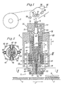
- the exemplary arrangement shown as a whole in FIG. 1 serves to mount onto a metallic strip-shaped substrate 4 (lead frame), which is transported in steps in the direction of arrow c is to solder semiconductor chips 8 using soft solder.
- a solder wire 1 (Diameter e.g. 1 mm or 0.76 mm) is drawn off from a coil 2 with the help of Drive means 3 advanced longitudinally from top to bottom by a device 5 and melted in the lower area.
- the device 5 is liftable as a whole lowerable (arrow a).
- Liquid solder 1 ' is discharged in individual portions Step-by-step actuation of the drive 3, in the present example via a form stamp 6 in each case with the device 5 lowered, with the die resting on the substrate 4 (see Fig. 6).
- solder 1 The heated, metallic substrate 4 is wetted by the solder.
- the facility 5 is then lifted and the substrate 4 is transported further with the solder portion 1 ′′ taken over, whereupon, as only indicated schematically, a chip 8 on the still liquid portion of solder 1 " is placed.
- the approximately vertical device 5 consists essentially of a tubular Housing 10, a guide part 12, a connecting part 14, a melting unit 18 with Form stamp 6, and the drive 3.
- the guide part 12 and the connecting part 14 are in Housing 10 permanently installed.
- the melting unit 18 together with the die 6 can on the other hand, perform a certain vertical stroke along the guide part 12 (arrow b).
- the guide part 12 has a downwardly projecting tube 13. Inside the tube 13 there are two more, concentric tubes 15 and 17, from the head 16 of the connector 14 going out. The lower ends of the tubes 15 and 13 are centered on each other. Through the The solid solder 1 extends longitudinally through the inner tube 15. A lower section 15 ' this longitudinal bore is expanded by a guide tube 20 which leads to the melting unit 18 heard to record smoothly. The longitudinal bore 21 of the guide tube 20 extends to Exit end 22 and is the diameter of the solid, wire or rod-shaped soft solder 1 adjusted (maximum about 5-10% excess).
- the melting unit 18 is of an annular, fixedly mounted in the interior of the housing 10, surrounded electric heater 25. It heats a cylindrical crucible 26 without contact, the upper end of which is held by a sleeve 27. The latter is via a ball guide guided on the tube 13. Crucible 26 and guide tube 20 are at their lower ends firmly connected.
- the crucible 26 From the heater 25, the crucible 26 and from this a lower area of the vertical Guide tube 20 including the lower tube end 22 for melting the solder heated so that there is molten solder 1 'in the bore 21 below in the tube 20.
- the temperature in the heated, lower area of the tube 20 is generally higher than the liquidus temperature of the solder material, so that the solder is then complete is melted;
- certain solder alloys can also be used at temperatures below Liquidus temperature are processed at which the solder material is only partially molten is (solid / liquid mixture). The latter case should therefore always be included, even if in the following we simply speak of "molten” or "melt”. How else is executed in more detail, each by actuating the drive 3 or feeding the fixed Lots 1 in the guide tube 20 a portion of liquid solder 1 'from the bottom of the hole 21 be expelled. In the present case, the discharge takes place in the form stamp 6 the sprue channel 62, which narrowed one adjoining the bore 21 Forms outlet mouth.
- connection part 14 contains an arrangement for the circulation of a suitable one Cooling medium, e.g. Compressed air.
- the cooling medium is supplied through a channel 51 and flows then in the bore of the tube 17 outside along the tube 15 down to one Ring channel 52 and from there along the pipe 17 up again to the outlet channel 53.
- the guide tube 20 is thereby over the thin-walled lower portion of the tube 15 Cooled in the upper region y, preferably with a constantly regulated cooling capacity.
- the temperature transition through the interaction of (regulated) heating and cooling proves to be very stable in operation.
- the fill level of the melt in the bore 21 and so that the amount of melt that is available before the ejection is on this Way controlled.
- the narrowed outlet mouth 62 makes it possible to hold the Melt, even if the capillary action in the bore 21 and the cohesion of the Melt would not be enough.
- the narrowing mouth 62 is used below 7 executed further.
- the solid solder 1 When the solid solder 1 is advanced, it acts as a piston in the bore 21 on the liquid solder 1 '.
- the advanced, fixed section is immediately up to The height of the stable temperature transition melted.
- the heating output is in the essentially according to the amount of solder to be discharged per unit of time during operation.
- At the end of fixed wire section automatically creates a certain sealing effect during the ejection process a by penetrating into the guide gap between the wire and the bore wall
- the melt immediately solidifies and is pushed along on the wire.
- the drive means 3 for the gradual advancement of the wire or rod-shaped solder 1 1 have a drive roller 31 and a feeler roller 32, between which the solder is passed through.
- the drive roller 31 is a motor 30, advantageously a Stepper motor, which receives a feed signal from a controller 34.
- the Feed signal is derived in the controller on the one hand from an input signal 35, that of the respective quantity of solder to be ejected corresponds to the setpoint value, and on the other hand one Position measuring signal as actual value of the feed path, generated by a rotary encoder (encoder) 33, which is connected to the feeler roller 32. Because a constant cross section of the solid used Solder can be assumed corresponds to a certain feed path of the solder wire 1 exactly a certain volume of the ejected through the outlet mouth 22, liquid portion of solder.
- the Form stamp 6 is made by means of gimbals, as can be seen in particular from FIG. 2 is held in contact with the spherical surface 24.
- a gimbal 40 is on one Ring diameter held on two rods 42 pivoted upwards in the Extend housing 10 and stuck in a support ring 44; the support ring 44 lies on the housing loose on.
- Different form stamps can also be easily exchanged for one another.
- the the die used in each case is raised for this purpose, with the crucible 26 and the sleeve 27, the compression spring 29 is compressed.
- the collar 64 is then rotated over the bearing pins 45 until the Grooves 65 are approximately aligned with the rods 42 and the stamp is removed downwards can be.
- the Construction ensures a high positional accuracy of the same, so that after the exchange no adjustment is necessary.
- the crucible 26 together with the tube 20 the only parts of the device that come into contact with liquid solder occur and can therefore be exposed to a certain amount of pollution.
- construction advantageously allows a simple, quick and reproducible Also replace the crucible 26 with the tube 20.
- the die 6 is also heated to the working temperature T H of the solder via the spherical surface 24.
- the form stamp 6 - like the crucible 26 and the guide tube 20 are made of a material which is not wettable by the molten solder 1 '. Suitable materials are, for example, graphite, ceramic, glass or also stainless steel and titanium.
- the mold cavity 61 of the Form stamp 6 is located on the underside of the body 60, is by a support edge 66 limited and is open towards the bottom of the substrate. Over one of the spherical surface 24 outgoing, relatively narrow sprue 62 communicates with the mold cavity 61 Outlet mouth 22 on the guide tube 20.
- Rising channels 63 are present, which extend from the cavity 61 and are open at the top. Such riser channels are preferably located in the corners or in, as shown Edge areas of the mold cavity to complete and quick mold filling guarantee; of course, the arrangement of riser channels is according to the selected geometry of the mold cavity.
- the surface area of the mold cavity in turn depends on that of the chips to be soldered.
- the plotted, molten solder portions are (as is known per se) during the subsequent application of the chip "squeezed" by it in the soldering gap until the chip is fully wetted and of the substrate.
- the lower area shows x Guide tube 20 a certain supply of liquid solder 1 'ready.
- the device is now lowered (arrow a) until the die 6 is seated on the Substrate 4. This lowering takes place with a small overstroke, so that the spring 29 somewhat compressed and the ring 44 is lifted off.
- the spring 29 also dampens the shock of the die 6 striking the substrate.
- the gimbal mounted fits Form stamp 6 under the spring action of a possible, slight skew of the substrate 4th exactly and the support edge 66 closes the mold cavity 61 tightly. Through the overstroke there are also certain tolerances in the height of the substrate and in the manufacturing height the form stamp bridges.
- the cycle time can be shortened overall by changing the Partially overlap periods for lowering and solder ejection. But especially the solder drop that has already been ejected - if the distance of the Form stamp 6 above the substrate - already laterally over a significant part of the Spread out the mold surface and wet the substrate, unhindered by the generally very small height of the mold cavity 61 (the depth of the recess 61 in the body 60 is mostly significantly less than that shown in FIGS. 1, 4 and 6 for the sake of clarity). The lateral spreading of the liquid solder up to the edges of the mold cavity continues, while the punch 6 is fully placed on the substrate.
- riser channels 63 - ensuring full mold filling - was already mentioned above. It is advantageous to compare the one formed by the channels 63 (in comparison with the volume of the mold cavity 61) to make targeted use of the storage volume, by choosing the height of the room 61 a little lower than to generate the required Solder layer thickness (after mounting the chip) would be required. A significant part of the required portion of solder then inevitably gets into the mold stamp (Fig. 6) Riser channels 63, with very great certainty, even with certain variations of the ejected volume, also the corners and edges of the molding surface are wetted. At the subsequent lifting of the die 6 flows in the channels 63 stored The amount of solder immediately returns and is distributed over the wetted area. Finally, it can the solder feed or the portion size within the storage volume of the Rising channels 63 can be varied to correspond with one and the same punch 6 to achieve different final layer thicknesses in the solder gap.
- the device 5 After the solder feed has ended and the solder portion has been ejected, the device 5 immediately becomes lifted off the substrate.
- the liquid solder adheres to the substrate and tears in the channel 62 under the mouth 22; the liquid solder present in the channels 63 is distributed as mentioned above the surface wetted by the solder.
- the heated substrate 4 is then known One step forward (arrow c), so that a new substrate field under the Device arrives and a chip 8 on the just applied, still liquid portion of solder 1 " can be placed. A new work cycle can now begin.
- solder portion that is discharged is in each case within the bore 62 tears off.
- the point of separation within the length of the bore is indefinite, which is a means some variation in the size of the consecutive portions.
- this spread can be reduced by shortening the bore 62 7, after which the bore at 62a is widened from above. This ensures that the melt can only tear off in the short bore piece 62.
Landscapes
- Engineering & Computer Science (AREA)
- Mechanical Engineering (AREA)
- Die Bonding (AREA)
- Electric Connection Of Electric Components To Printed Circuits (AREA)
Description
- Fig. 1
- zeigt im Vertikalschnitt und teilweise schematisch eine Einrichtung mit einem Formstempel zum Weichlöten von Halbleiter-Chips auf einem metallischen Substrat,
- Fig. 2
- ist ein Horizontalschnitt auf der Höhe der Linie II-II in Fig. 1,
- Fig. 3
- zeigt die Ansicht von unten des bei der Einrichtung nach Fig. 1 verwendeten Formstempels,
- Fig. 4
- ist die teilweise geschnittene Seitenansicht und
- Fig. 5
- die Draufsicht des gleichen Formstempels,
- Fig. 6
- zeigt im Schnitt den auf dem Substrat aufliegenden Formstempel mit in den Formhohlraum ausgestossener Lotportion, und
- Fig. 7
- zeigt im grösseren Massstab eine besondere Ausführung der verengten Austrittsmündung.
Claims (4)
- Formstempel (6) zum Austragen von flüssigem Lot (1'), der einen mit einem Eingusskanal (62) verbundenen, nach unten offenen Formhohlraum (61) aufweist, dadurch gekennzeichnet, dass der Formstempel (6) aus einem vom geschmolzenen Lot nicht benetzbaren Material besteht und dass der Eingusskanal (62) auf der dem Formhohlraum (61) abgewandten Seite mit einem abrupten Übergang aufgeweitet ist.
- Formstempel (6) nach Anspruch 1, dadurch gekennzeichnet, dass der Formstempel (6) vom Formhohlraum (61) ausgehende Steigerkanäle (63) zur Aufnahme von flüssigem Lot (1') aufweist, deren Speichervolumen einen Teil des auszutragenden Lotes aufzunehmen vermag.
- Formstempel (6) nach Anspruch 1 oder 2, gekennzeichnet durch mehrere separate Formhohlräume.
- Formstempel (6) nach einem der Ansprüche 1 bis 3, dadurch gekennzeichnet, dass der Eingusskanal (62) auf der dem Formhohlraum (61) zugewandten Seite so eng ist, dass das geschmolzene Lot infolge Kapillarwirkung nicht von selbst ausfliesst.
Applications Claiming Priority (3)
| Application Number | Priority Date | Filing Date | Title |
|---|---|---|---|
| CH192695 | 1995-07-01 | ||
| CH192695 | 1995-07-01 | ||
| EP96110030A EP0752294B1 (de) | 1995-07-01 | 1996-06-21 | Verfahren und Einrichtung zum Austragen von flüssigem Lot |
Related Parent Applications (1)
| Application Number | Title | Priority Date | Filing Date |
|---|---|---|---|
| EP96110030A Division EP0752294B1 (de) | 1995-07-01 | 1996-06-21 | Verfahren und Einrichtung zum Austragen von flüssigem Lot |
Publications (3)
| Publication Number | Publication Date |
|---|---|
| EP0970774A2 EP0970774A2 (de) | 2000-01-12 |
| EP0970774A3 EP0970774A3 (de) | 2000-03-29 |
| EP0970774B1 true EP0970774B1 (de) | 2002-07-24 |
Family
ID=4221830
Family Applications (2)
| Application Number | Title | Priority Date | Filing Date |
|---|---|---|---|
| EP96110030A Expired - Lifetime EP0752294B1 (de) | 1995-07-01 | 1996-06-21 | Verfahren und Einrichtung zum Austragen von flüssigem Lot |
| EP99113056A Expired - Lifetime EP0970774B1 (de) | 1995-07-01 | 1996-06-21 | Formstempel zum Austragen von flüssigem Lot |
Family Applications Before (1)
| Application Number | Title | Priority Date | Filing Date |
|---|---|---|---|
| EP96110030A Expired - Lifetime EP0752294B1 (de) | 1995-07-01 | 1996-06-21 | Verfahren und Einrichtung zum Austragen von flüssigem Lot |
Country Status (6)
| Country | Link |
|---|---|
| US (1) | US5878939A (de) |
| EP (2) | EP0752294B1 (de) |
| KR (1) | KR100253995B1 (de) |
| DE (2) | DE59609491D1 (de) |
| SG (1) | SG67355A1 (de) |
| TW (1) | TW320578B (de) |
Families Citing this family (35)
| Publication number | Priority date | Publication date | Assignee | Title |
|---|---|---|---|---|
| US6053398A (en) * | 1996-12-06 | 2000-04-25 | The Furukawa Electric Co., Ltd. | Solder bump forming method, solder bump forming apparatus, head unit for use therein and soldering method using the head unit |
| US6224180B1 (en) | 1997-02-21 | 2001-05-01 | Gerald Pham-Van-Diep | High speed jet soldering system |
| US6006639A (en) * | 1998-02-04 | 1999-12-28 | Litton Systems, Inc. | Solder placement apparatus and method |
| EP0987516A1 (de) * | 1998-09-15 | 2000-03-22 | ESEC Management SA | Einrichtung zur Erfassung des Zeitpunktes, an dem sich zwei elektrisch leitende Körper oder ein elektrisch leitender Körper und ein elektrisch leitender Flüssigkeitstropfen berühren |
| DE10042661B4 (de) | 1999-09-10 | 2006-04-13 | Esec Trading S.A. | Verfahren und Vorrichtungen für die Montage von Halbleiterchips |
| JP4346054B2 (ja) | 2000-01-18 | 2009-10-14 | 栄修 永田 | ハンダ付け方法およびハンダ付け装置 |
| SG91867A1 (en) * | 2000-05-24 | 2002-10-15 | Casem Asia Pte Ltd | Improved apparatus and method for dispensing solder |
| SG91870A1 (en) * | 2000-05-26 | 2002-10-15 | Casem Asia Pte Ltd | Method and device for bleed out control in solder bonding |
| EP1264654A1 (de) * | 2001-06-08 | 2002-12-11 | Esec Trading S.A. | Verfahren und Einrichtung zum Auftragen von Lot |
| SG106126A1 (en) * | 2002-03-08 | 2004-09-30 | Esec Trading Sa | Method and apparatus for dispensing solder on a substrate |
| EP1342525A1 (de) * | 2002-03-08 | 2003-09-10 | ESEC Trading SA | Verfahren und Einrichtung zum Auftragen von Lot auf ein Substrat |
| EP1393845B1 (de) * | 2002-03-08 | 2006-09-20 | Unaxis International Trading Ltd | Verfahren und Einrichtung zum Auftragen von Lot auf ein Substrat |
| SE0202247D0 (sv) * | 2002-07-18 | 2002-07-18 | Mydata Automation Ab | Jetting device and method at a jetting device |
| DE102004059281B3 (de) * | 2004-12-09 | 2006-04-13 | Mühlbauer Ag | Thermodeneinheit für Halbleiterbauelemente |
| US20080308952A1 (en) * | 2005-07-28 | 2008-12-18 | Infineon Technologies Ag | Method for Reliably Positioning Solder on a Die Pad for Attaching a Semiconductor Chip to the Die Pad and Molding Die for Solder Dispensing Apparatus |
| US8011563B2 (en) * | 2006-04-05 | 2011-09-06 | International Business Machines Corporation | Compliant mold fill head with integrated cavity venting and solder cooling |
| US7735715B2 (en) * | 2007-12-07 | 2010-06-15 | Asm Assembly Automation Ltd | Dispensing solder for mounting semiconductor chips |
| US7931187B2 (en) * | 2008-11-12 | 2011-04-26 | International Business Machines Corporation | Injection molded solder method for forming solder bumps on substrates |
| US7980446B2 (en) | 2009-03-06 | 2011-07-19 | International Businss Machines Corporation | Micro-fluidic injection molded solder (IMS) |
| US20100243712A1 (en) * | 2009-03-27 | 2010-09-30 | Ats Automation Tooling Systems Inc. | Thermode, clamping arrangment therefor, and method of manufacture |
| CH705035B1 (de) | 2011-05-23 | 2016-03-31 | Esec Ag | Verfahren zum Auftragen von Lot auf ein Substrat und Verfahren für die Montage eines Halbleiterchips. |
| CH704991A1 (de) * | 2011-05-23 | 2012-11-30 | Esec Ag | Verfahren zum Auftragen von Lot auf ein Substrat und Verfahren für die Montage von Halbleiterchips. |
| JP5800778B2 (ja) * | 2011-11-25 | 2015-10-28 | 三菱電機株式会社 | 接合方法および半導体装置の製造方法 |
| CH706712A1 (de) | 2012-07-05 | 2014-01-15 | Besi Switzerland Ag | Verfahren und Vorrichtung zum Auftragen von Lot auf ein Substrat. |
| CN102810489B (zh) * | 2012-08-17 | 2015-01-21 | 杭州士兰集成电路有限公司 | 芯片封装系统、方法、注入装置及冲压与注入联动装置 |
| CH708278A1 (de) * | 2013-07-08 | 2015-01-15 | Besi Switzerland Ag | Vorrichtung zum Auftragen und Verteilen von Lot auf einem Substrat. |
| DE102013110402A1 (de) | 2013-09-20 | 2015-03-26 | Smart Pac Gmbh Technology Services | Anordnung und Verfahren zum reproduzierbaren Aufbringen kleiner Flüssigkeitsmengen |
| JP6703733B2 (ja) * | 2015-10-16 | 2020-06-03 | 株式会社アンド | 半田鏝の鏝先及び半田付け装置 |
| CN105215499B (zh) * | 2015-10-19 | 2017-10-20 | 周海兵 | 点焊焊锡装置 |
| US11569011B2 (en) * | 2016-11-04 | 2023-01-31 | John Howard | Method and apparatus for reinforcing a cable used in high frequency applications |
| DE102017121600A1 (de) * | 2017-09-18 | 2019-03-21 | Marco Systemanalyse Und Entwicklung Gmbh | Dosierventil und Dosierverfahren |
| US20200189018A1 (en) * | 2018-12-14 | 2020-06-18 | Lear Corporation | Apparatus and method for automated soldering process |
| CN114005776B (zh) * | 2021-11-15 | 2022-09-13 | 盐城矽润半导体有限公司 | 一种半导体定位装配装置 |
| DE102023110438B4 (de) | 2023-04-24 | 2025-05-15 | Besi Switzerland Ag | Vorrichtung mit einer verbesserten Niederhaltevorrichtung |
| CN118081122B (zh) * | 2024-04-28 | 2024-07-05 | 江苏宿芯半导体有限公司 | 一种芯片晶圆加工用切割设备 |
Citations (1)
| Publication number | Priority date | Publication date | Assignee | Title |
|---|---|---|---|---|
| JPH01249163A (ja) * | 1988-03-31 | 1989-10-04 | Seiko Epson Corp | ディスペンサー用ノズル及びそれを備えたダイボンダー |
Family Cites Families (17)
| Publication number | Priority date | Publication date | Assignee | Title |
|---|---|---|---|---|
| US1561924A (en) * | 1924-01-23 | 1925-11-17 | William W Weitling | Metal founding |
| US2875719A (en) * | 1956-02-29 | 1959-03-03 | Smith Raymond | Solder feeding attachment for a soldering iron |
| AT291716B (de) * | 1969-03-26 | 1971-07-26 | Klaus Schlitt Loettechhnik Mec | Einhand-Lötpistole |
| US3679341A (en) * | 1970-09-25 | 1972-07-25 | Owens Illinois Inc | Apparatus for impact injection molding of plastic articles |
| JPS537458B1 (de) * | 1971-05-15 | 1978-03-17 | ||
| JPS5866020A (ja) * | 1981-10-15 | 1983-04-20 | Toshiba Corp | 液の定量吐出装置 |
| US4520861A (en) * | 1983-11-18 | 1985-06-04 | Republic Steel Corporation | Method and apparatus for alloying continuously cast steel products |
| US4577398A (en) * | 1984-09-07 | 1986-03-25 | Trilogy Computer Development Partners, Ltd. | Method for mounting a semiconductor chip |
| US4709849A (en) * | 1985-11-27 | 1987-12-01 | Fry Metals, Inc. | Solder preform and methods employing the same |
| JPS62181118A (ja) * | 1986-02-05 | 1987-08-08 | Showa Denko Kk | 成形用金型 |
| DE3612341A1 (de) * | 1986-04-11 | 1987-10-15 | Franz Ummen | Einhandloetgeraet mit lotinjektor |
| DE3734550A1 (de) * | 1987-10-13 | 1989-04-27 | Franz Ummen | Hochfrequenzbeheizter lotinjektor |
| EP0311711A1 (de) * | 1987-10-16 | 1989-04-19 | KLEVOTEC Gesellschaft für rechnergestützte Systemanwendungen mbH&Co.KG | Sintervorrichtung für Formlinge mit Hinterschneidungen aus schäumbarem Kunststoff |
| US5042708A (en) * | 1990-09-24 | 1991-08-27 | International Business Machines Corporation | Solder placement nozzle assembly |
| DE4136723A1 (de) * | 1991-11-08 | 1993-05-13 | U T S Uhrentechnik Schwarzwald | Pastenloetvorrichtung |
| US5316700A (en) * | 1992-11-02 | 1994-05-31 | Wesley-Jessen Corporation | Method and apparatus for removing excess lens forming material |
| JP3583462B2 (ja) * | 1993-04-05 | 2004-11-04 | フォード モーター カンパニー | 電子成分のための微小はんだ付け装置および方法 |
-
1996
- 1996-06-21 DE DE59609491T patent/DE59609491D1/de not_active Expired - Lifetime
- 1996-06-21 EP EP96110030A patent/EP0752294B1/de not_active Expired - Lifetime
- 1996-06-21 EP EP99113056A patent/EP0970774B1/de not_active Expired - Lifetime
- 1996-06-21 DE DE59605457T patent/DE59605457D1/de not_active Expired - Lifetime
- 1996-06-25 TW TW085107611A patent/TW320578B/zh not_active IP Right Cessation
- 1996-06-27 KR KR1019960024336A patent/KR100253995B1/ko not_active Expired - Fee Related
- 1996-06-28 SG SG1996010175A patent/SG67355A1/en unknown
- 1996-06-28 US US08/672,748 patent/US5878939A/en not_active Expired - Fee Related
Patent Citations (1)
| Publication number | Priority date | Publication date | Assignee | Title |
|---|---|---|---|---|
| JPH01249163A (ja) * | 1988-03-31 | 1989-10-04 | Seiko Epson Corp | ディスペンサー用ノズル及びそれを備えたダイボンダー |
Also Published As
| Publication number | Publication date |
|---|---|
| SG67355A1 (en) | 1999-09-21 |
| TW320578B (de) | 1997-11-21 |
| EP0752294A2 (de) | 1997-01-08 |
| EP0970774A3 (de) | 2000-03-29 |
| EP0752294B1 (de) | 2000-06-21 |
| KR970008363A (ko) | 1997-02-24 |
| DE59609491D1 (de) | 2002-08-29 |
| DE59605457D1 (de) | 2000-07-27 |
| EP0970774A2 (de) | 2000-01-12 |
| US5878939A (en) | 1999-03-09 |
| EP0752294A3 (de) | 1998-05-20 |
| KR100253995B1 (ko) | 2000-05-01 |
Similar Documents
| Publication | Publication Date | Title |
|---|---|---|
| EP0970774A2 (de) | Formstempel zum Austragen von flüssigem Lot | |
| DE69632795T3 (de) | Verfahren und Vorrichtung zur Ausgabe von kleinen Mengen eines flüssigen Materials | |
| WO2018167209A1 (de) | Druckkopf für den 3d-druck von metallen | |
| DE10393767T5 (de) | Spritzgießeinheit in einer Kaltkammer-Druckgussmaschine und darin angewandtes Dosierverfahren | |
| EP2148574A1 (de) | Vorrichtung zum giessen von verzehrprodukten | |
| WO2020069910A1 (de) | Dosiersystem mit dosierstoff-kühleinrichtung | |
| DE102014226286A1 (de) | Schmelzmetallauslassvorrichtung und Verfahren zum Auslassen von geschmolzenem Metall | |
| DE69919809T2 (de) | Mikrospritzgiessmaschine | |
| DE2254033A1 (de) | Vorrichtung zum punktweisen auftragen eines klebstoffes | |
| EP3046711B1 (de) | Anordnung und verfahren zum reproduzierbaren aufbringen kleiner flüssigkeitsmengen | |
| CH708335B1 (de) | Vorrichtung zum Auftragen und Verteilen von flussmittelfreiem Lot auf einem Substrat. | |
| DE1935398C3 (de) | Schmelz- und Abgabevorrichtung für thermoplastisches Material | |
| DE2754738A1 (de) | Extrusionskopf | |
| DE4133224A1 (de) | Vorrichtung zum loeten von flachbaugruppen | |
| DE3640620C2 (de) | ||
| DE4414005C2 (de) | Verfahren zum Ummanteln von elektronischen Bauteilen | |
| EP0342254A1 (de) | Vorrichtung zum Aufschmelzen von hochpolymeren, thermoplastischen Werkstoffen, insbesondere Klebstoffen | |
| DE102013220366A1 (de) | Dosieranlage | |
| EP1264654A1 (de) | Verfahren und Einrichtung zum Auftragen von Lot | |
| DE102022108717B4 (de) | Extruderventil für einen extrusionsbasierten, thermoplastischen Materialaustrag sowie Verfahren zum extrusionsbasierten, thermoplastischen Materialaustrag | |
| DE102021116983B4 (de) | Schneckensystem einer Werkzeugmaschine zur additiven Fertigung, Werkzeugmaschine und Verfahren zum Betreiben einer Werkzeugmaschine | |
| DE4038304A1 (de) | Mit elektromagnetischem hub arbeitende stranggusseinrichtung | |
| DE19601055B4 (de) | Verfahren und Vorrichtung zum Beloten von Flächen | |
| DE733863C (de) | Pressgiessmaschine zum Verarbeiten von Magnesium und seinen Legierungen | |
| AT128389B (de) | Maschine zur Herstellung von Durchschuß, Zeilen und Linien für Druckereien. |
Legal Events
| Date | Code | Title | Description |
|---|---|---|---|
| PUAI | Public reference made under article 153(3) epc to a published international application that has entered the european phase |
Free format text: ORIGINAL CODE: 0009012 |
|
| AC | Divisional application: reference to earlier application |
Ref document number: 752294 Country of ref document: EP |
|
| AK | Designated contracting states |
Kind code of ref document: A2 Designated state(s): CH DE FR GB IT LI |
|
| AX | Request for extension of the european patent |
Free format text: AL PAYMENT 19990805;LT PAYMENT 19990805;LV PAYMENT 19990805;MK PAYMENT 19990805;RO PAYMENT 19990805;SI PAYMENT 19990805 |
|
| PUAL | Search report despatched |
Free format text: ORIGINAL CODE: 0009013 |
|
| AK | Designated contracting states |
Kind code of ref document: A3 Designated state(s): AT BE CH CY DE DK ES FI FR GB GR IE IT LI LU MC NL PT SE |
|
| AX | Request for extension of the european patent |
Free format text: AL PAYMENT 19990805;LT PAYMENT 19990805;LV PAYMENT 19990805;MK PAYMENT 19990805;RO PAYMENT 19990805;SI PAYMENT 19990805 |
|
| 17P | Request for examination filed |
Effective date: 20000929 |
|
| AKX | Designation fees paid |
Free format text: CH DE FR GB IT LI |
|
| AXX | Extension fees paid |
Free format text: AL PAYMENT 19990805;LT PAYMENT 19990805;LV PAYMENT 19990805;MK PAYMENT 19990805;RO PAYMENT 19990805;SI PAYMENT 19990805 |
|
| 17Q | First examination report despatched |
Effective date: 20001228 |
|
| RAP1 | Party data changed (applicant data changed or rights of an application transferred) |
Owner name: ESEC TRADING SA |
|
| GRAG | Despatch of communication of intention to grant |
Free format text: ORIGINAL CODE: EPIDOS AGRA |
|
| GRAG | Despatch of communication of intention to grant |
Free format text: ORIGINAL CODE: EPIDOS AGRA |
|
| GRAH | Despatch of communication of intention to grant a patent |
Free format text: ORIGINAL CODE: EPIDOS IGRA |
|
| GRAH | Despatch of communication of intention to grant a patent |
Free format text: ORIGINAL CODE: EPIDOS IGRA |
|
| GRAA | (expected) grant |
Free format text: ORIGINAL CODE: 0009210 |
|
| AC | Divisional application: reference to earlier application |
Ref document number: 752294 Country of ref document: EP |
|
| AK | Designated contracting states |
Kind code of ref document: B1 Designated state(s): CH DE FR GB IT LI |
|
| DAX | Request for extension of the european patent (deleted) | ||
| REG | Reference to a national code |
Ref country code: GB Ref legal event code: FG4D Free format text: NOT ENGLISH |
|
| REG | Reference to a national code |
Ref country code: CH Ref legal event code: EP |
|
| REF | Corresponds to: |
Ref document number: 59609491 Country of ref document: DE Date of ref document: 20020829 |
|
| REG | Reference to a national code |
Ref country code: CH Ref legal event code: NV Representative=s name: PATENTANWALTSBUERO DR. URS FALK |
|
| GBT | Gb: translation of ep patent filed (gb section 77(6)(a)/1977) |
Effective date: 20020919 |
|
| ET | Fr: translation filed | ||
| PLBE | No opposition filed within time limit |
Free format text: ORIGINAL CODE: 0009261 |
|
| STAA | Information on the status of an ep patent application or granted ep patent |
Free format text: STATUS: NO OPPOSITION FILED WITHIN TIME LIMIT |
|
| PGFP | Annual fee paid to national office [announced via postgrant information from national office to epo] |
Ref country code: GB Payment date: 20030602 Year of fee payment: 8 |
|
| PGFP | Annual fee paid to national office [announced via postgrant information from national office to epo] |
Ref country code: FR Payment date: 20030618 Year of fee payment: 8 |
|
| 26N | No opposition filed |
Effective date: 20030425 |
|
| PG25 | Lapsed in a contracting state [announced via postgrant information from national office to epo] |
Ref country code: GB Free format text: LAPSE BECAUSE OF NON-PAYMENT OF DUE FEES Effective date: 20040621 |
|
| GBPC | Gb: european patent ceased through non-payment of renewal fee |
Effective date: 20040621 |
|
| PG25 | Lapsed in a contracting state [announced via postgrant information from national office to epo] |
Ref country code: FR Free format text: LAPSE BECAUSE OF NON-PAYMENT OF DUE FEES Effective date: 20050228 |
|
| REG | Reference to a national code |
Ref country code: FR Ref legal event code: ST |
|
| PG25 | Lapsed in a contracting state [announced via postgrant information from national office to epo] |
Ref country code: IT Free format text: LAPSE BECAUSE OF NON-PAYMENT OF DUE FEES Effective date: 20050621 |
|
| REG | Reference to a national code |
Ref country code: CH Ref legal event code: PUE Owner name: OERLIKON ASSEMBLY EQUIPMENT AG, STEINHAUSEN Free format text: ESEC TRADING SA#HINTERBERGSTR. 32, POSTFACH 5503#6330 CHAM (CH) -TRANSFER TO- OERLIKON ASSEMBLY EQUIPMENT AG, STEINHAUSEN#HINTERBERGSTRASSE 32#6330 CHAM (CH) |
|
| PGFP | Annual fee paid to national office [announced via postgrant information from national office to epo] |
Ref country code: CH Payment date: 20140612 Year of fee payment: 19 Ref country code: DE Payment date: 20140618 Year of fee payment: 19 |
|
| REG | Reference to a national code |
Ref country code: DE Ref legal event code: R119 Ref document number: 59609491 Country of ref document: DE |
|
| REG | Reference to a national code |
Ref country code: CH Ref legal event code: PL |
|
| PG25 | Lapsed in a contracting state [announced via postgrant information from national office to epo] |
Ref country code: DE Free format text: LAPSE BECAUSE OF NON-PAYMENT OF DUE FEES Effective date: 20160101 Ref country code: CH Free format text: LAPSE BECAUSE OF NON-PAYMENT OF DUE FEES Effective date: 20150630 Ref country code: LI Free format text: LAPSE BECAUSE OF NON-PAYMENT OF DUE FEES Effective date: 20150630 |