EP0969601A2 - Verfahren zur Verbesserung eines Nutzsignals in einem Funkempänger - Google Patents
Verfahren zur Verbesserung eines Nutzsignals in einem Funkempänger Download PDFInfo
- Publication number
- EP0969601A2 EP0969601A2 EP99111865A EP99111865A EP0969601A2 EP 0969601 A2 EP0969601 A2 EP 0969601A2 EP 99111865 A EP99111865 A EP 99111865A EP 99111865 A EP99111865 A EP 99111865A EP 0969601 A2 EP0969601 A2 EP 0969601A2
- Authority
- EP
- European Patent Office
- Prior art keywords
- signal
- amplifier
- strength detection
- detection unit
- wanted
- Prior art date
- Legal status (The legal status is an assumption and is not a legal conclusion. Google has not performed a legal analysis and makes no representation as to the accuracy of the status listed.)
- Granted
Links
Images


Classifications
-
- H—ELECTRICITY
- H04—ELECTRIC COMMUNICATION TECHNIQUE
- H04B—TRANSMISSION
- H04B1/00—Details of transmission systems, not covered by a single one of groups H04B3/00 - H04B13/00; Details of transmission systems not characterised by the medium used for transmission
- H04B1/06—Receivers
- H04B1/10—Means associated with receiver for limiting or suppressing noise or interference
- H04B1/109—Means associated with receiver for limiting or suppressing noise or interference by improving strong signal performance of the receiver when strong unwanted signals are present at the receiver input
-
- H—ELECTRICITY
- H03—ELECTRONIC CIRCUITRY
- H03G—CONTROL OF AMPLIFICATION
- H03G3/00—Gain control in amplifiers or frequency changers
- H03G3/20—Automatic control
- H03G3/30—Automatic control in amplifiers having semiconductor devices
- H03G3/3052—Automatic control in amplifiers having semiconductor devices in bandpass amplifiers (H.F. or I.F.) or in frequency-changers used in a (super)heterodyne receiver
- H03G3/3078—Circuits generating control signals for digitally modulated signals
Definitions
- the invention is based on a method for improving the wanted signal in a radio receiving unit.
- the invention is based on the object of providing a method for improving the wanted signal in a radio receiving unit. This object is achieved by the features of the invention specified in Claim 1. Advantageous developments of the invention are specified in the dependent claims.
- the method according to the invention for improving the wanted signal in a radio receiving unit having a channel filter, having a switch, having a control unit, having a signal-strength detection unit and having controllable amplifiers is distinguished in that the control unit drives the switch in such a manner that the switch alternately supplies a first signal upstream of the channel filter and a second signal downstream of the channel filter to the signal-strength detection unit, and that the output signal of the signal-strength detection unit, also referred to as the detector signal, is supplied to the control unit, and that the amplifiers are driven as a function of the two values of output signal.
- the amplifiers are driven in such a manner that an improved wanted signal is obtained by using the method according to the invention.
- the method is furthermore distinguished in that the first signal contains a wanted signal element and an interference signal element, and in that the interference signal element is filtered out by the channel filter.
- Elimination of the interference signals by using the channel filter allows the signal strengths to be evaluated with or without an interference signal.
- the method is also distinguished in that the first signal, upstream of the channel filter, is amplified by a first amplifier, and the second signal, downstream from the channel filter, is amplified by a second amplifier.
- the method is also characterized in that the gain setting is optimized such that the ratio N/(S+R) of the wanted signal N to the interference signals S and the noise R is as high as possible.
- the unit operates with high gain in the first amplifier, in order to keep receiver noise low.
- the gain in the first amplifier is high and powerful interference signals are present, only a low ratio N/(S+R) is in consequence achieved.
- An improved output signal can be obtained if the gain of the first amplifier is reduced, and the gain of the second amplifier is increased.
- the method is furthermore distinguished in that, if it is found by the control unit that the wanted signal is greater than the interference signals, maximum gain is set in the first amplifier, and a reduced gain is set in the second amplifier.
- the method is also distinguished in that, if the ratio N/(S+R) of the output signal is low when the gain of the first amplifier is at a minimum and severe interference sources are present, the frequency range is changed.
- the channel is changed in order in this way to improve the output signal by raising the wanted signal level in comparison with the interference source.
- Figure 1 shows a block diagram of the method according to the invention.
- the input signal ES passes via the first bandpass filter BF1, the mixer M, the first controllable amplifier RV1, and the second bandpass filter BF2 to the second controllable amplifier RV2, at whose output the wanted signal NS is present.
- the wanted signal NS is then supplied to an analogue/digital converter.
- a third controllable amplifier RV3 could also be arranged between the first bandpass filter BF1 and the mixer M. Since this is not absolutely essential, it is represented by dashed lines here.
- the controllable amplifier RV3 would be used for regulation improvement.
- the control unit SE contains a memory M.
- the memory is also represented by dashed lines, since this may be located outside the control unit SE.
- the control unit SE is furthermore connected to the first controllable amplifier RV1, to the PLL circuit (which is in turn connected to the mixer), to the switch S, to the second controllable amplifier RV2 and to the signal-strength detection unit RSSI. If a third controllable amplifier RV3 is used, it is also connected to the control unit. In a first switch position, the switch S passes a first signal S1 (upstream of the second bandpass filter BF2) to the signal-strength detection unit RSSI, and in a second switch position 2, it passes a second signal S2 (downstream from the second bandpass filter BF2) to the signal-strength detection unit RSSI.
- a schematic curve which indicates the band range from 902 to 928 MHz is shown in the first bandpass filter BF1, to which the input signal ES is supplied.
- the band range comprises a number of reception channels.
- the wanted signal is denoted by N, and interference signals by S.
- the input signal ES filtered in this way is then supplied to the mixer M.
- the mixer then mixes the signal with the signal from the PLL circuit, and passes this via the controllable amplifier VR1 on to the second bandpass filter BF2, which carries out the channel selection.
- the channel filter, for selecting the channel is in this case configured as a bandpass filter.
- the switch S1 switches to the switch position 1, where the signal-strength detection unit RSSI is supplied with the first signal S1 upstream of the second bandpass filter BF and, later, to the switch position 2, where the second signal S2, downstream from the second filter BF2 is supplied to the signal-strength detection unit RSSI.
- the output signal AS of the signal-strength detection unit RSSI is also supplied to the control unit SE. Since the output signal AS is a voltage value, the term output voltage is used in the following text. Via the control lines ST1, ST2 and, if appropriate, ST3, the control unit can on the one hand set the controllable amplifiers RV1 - RV3, and on the other hand knows the corresponding gain factors.
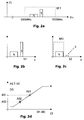
- Figures 2a-2d show the fundamental explanation of the measurement of the signal strengths.
- Figure 2a shows the spectrum of the input signal ES as a function of the input frequency fin.
- the bandpass filter BF1 limits the band range of the ISM band (Industrial Scientific Medical) between 900 MHz and 930 MHz.
- Figure 2b shows a first spectrum S1, in which a wanted signal N and an interference signal S are shown.
- the interference signal S is greater than the wanted signal N.
- Figure 2c shows a spectrum S2, in which a wanted signal N and a smaller interference signal S are shown.
- Figure 2d shows the output voltage AS as a function of the signal strength of the input signal ES.
- the output voltages for the respective spectrum S1 from Figure 2b and the spectrum S2 from Figure 2c are denoted by AS1 and AS2, respectively.
- the characteristic K indicates the characteristic profile of the signal-strength detection unit RSSI.
- the output voltage AS1 for the spectrum S1 from Figure 2b was obtained upstream of the bandpass filter BF2.
- the output voltage AS2 for the spectrum S2 from Figure 2c was obtained downstream from the bandpass filter BF2.
- the value by which the output voltage AS1 is greater than the output voltage AS2 is a measure of the strength of the interference signals in the adjacent channels.
- Figures 2e to 2i show the optimization of the gain setting for the situation in which a number of strong interference sources and a small wanted signal are present.
- Figure 2e shows that two interference signals S1 and S2 are present, which are greater than the wanted signal N.
- Figure 2f in turn shows the first spectrum S1 upstream of the bandpass filter BF2, in which case the intermodulation products I have been represented by dashed lines, and the basic noise has been denoted by R.
- Figure 2g shows the second spectrum S2, which is obtained downstream from the bandpass filter BF2. It can be seen that the ratio N/(S+R+I) of the wanted signal N to the interference signal S, the basic noise R and the intermodulation product I has deteriorated.
- Figure 2h shows the profile once the gain setting has been optimized, in such a manner that the first amplifier RV1 has produced less gain.
- the signal elements of the interference signal S1, S2 of the wanted signal N and the intermodulation product I have been reduced.
- Figure 2i is compared to Figure 2g, it can be seen that the interference signal elements S1, S2 and the intermodulation products I have been reduced to a major extent, and the ratio N(S+R+I) is thus better.
- the output voltage AS1 of the signal-strength detection unit RSSI is considerably greater than the output voltage AS2.
- the optimum gain setting in this situation now differs in that a low gain was used first of all, followed by an increased gain. As can be seen in Figures 2f to 2i, this has improved the ratio N/(S+R+I) .
- Figures 2j to 2p show a further situation for improving the gain setting.
- Figure 2j shows a small wanted signal N and a very small interference signal S.
- Figure 2k shows the spectrum S1 with normal gain.
- Figure 21 shows the spectrum S2, in which it can be seen that this now includes only a basic noise R as the interference element.
- Figure 2m shows that further amplification by the amplifier RV2 amplifies the wanted signal N as well as the basic noise R.
- Figure 2n shows that the gain in the first amplifier RV1 is increased so that the wanted signal N is increased as well as the interference signal S.
- Figure 2o shows that the bandpass filter BF1 has eliminated the interference signal S, and the wanted signal N is completely available.
- Figure 2p shows that, with further amplification by the amplifier RV2, the wanted signal N as well as the basic noise R are now amplified, with the basic noise not having been amplified to the same extent as that illustrated in Figure 2m, which was preceded by reduced amplification by the amplifier RV1. If a third amplifier RV3, which has been represented by dashed lines, is used in this case, the basic noise R can be reduced still further by maximum amplification by the amplifier RV3. This is feasible since the output voltage AS1 is approximately of the same magnitude as the output voltage AS2.
- Figures 2q to 2v show a channel change, since strong interference signals are present in the vicinity.
- Figure 2q shows the input signal ES as a function of the output frequency fin. The band region is indicated by BB.
- the interference signal S1 is located directly alongside the wanted signal N. In the first spectrum S1, it can be seen that a large proportion of intermodulation products I is scattered in the wanted signal N. The intermodulation product I is still present in the second spectrum S2.
- the interference source S1 is located directly alongside the wanted signal N.
- the output voltage AS1 is somewhat greater than the output voltage AS2 and, in this situation, we have a low gain factor for the amplifier RV1 upstream of the channel filter.
- Figure 2t shows that a channel change has been carried out, so that the wanted signal N is further away from the interference signal S1.
- the different channels are denoted by K1 to K3.
- the amplifier RV1 is now set to a low gain, so that the wanted signal N, the interference signal S1 and the intermodulation product I do not become excessively great.
- the spectrum S1 in Figure 2v shows that the wanted signal N is considerably greater than the interference signal S1, so that the output voltage AS1 is considerably greater than the output voltage AS2. It can clearly be seen here that the channel change has resulted in an improvement in the output voltage.
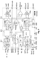
- FIG 3 shows an implementation of the method illustrated in Figure 1, in an analogue IC.
- Those components which are relevant for the invention are provided with the same component designation, and the method of operation is identical to that in the block diagram in Figure 1. It can clearly be seen that the signal path is split in two, into an I channel and a Q channel.
- the method according to the invention can thus also be used for communications systems with quadrature modulation.
- the control unit is illustrated separately here, on the one hand and the gain control logic SE1 for the first control amplifier RV1 and R'V1 and a further control unit SE2, which drives the second controllable amplifier RV2 and a further, second controllable amplifier R'V2.
- the respective switches for S, S' then supply the signals to the signal-strength detection unit RSSI.
- the method of operation of this circuit corresponds to the function described in Figure 1 and Figure 2.
- the controllable amplifier RV3 and the mixer are not illustrated in this figure, and have not been taken into account.
- the first controllable amplifier RV1, R'V1 contain an amplifier and a first bandpass filter BF1.
- the second controllable amplifiers RV2, R'V2 are split into a number of amplifiers, in order to allow a greater gain variation range.
- the first controllable amplifiers RV1, R'V1 are designed in order to allow a gain of between -6 dB and +18 dB.
- the first control unit SE1 is influenced by the gain factors Gain1 and Gain2, and the second control unit SE2 is influenced by the voltage VAGC.
- Part of the control unit is implemented in an IC, not shown here. This part drives the switch positions via RSSImode, thus knows the switch position, and thus knows the present mode of the signal-strength detection unit RSSI, that is to say which measured value or output voltage is being detected at the moment. This part then evaluates the output voltage AS, and supplies the control voltages Gain1, Gain2, VAGC for gain setting.
Landscapes
- Engineering & Computer Science (AREA)
- Computer Networks & Wireless Communication (AREA)
- Signal Processing (AREA)
- Noise Elimination (AREA)
- Amplifiers (AREA)
- Control Of Amplification And Gain Control (AREA)
- Circuits Of Receivers In General (AREA)
Applications Claiming Priority (2)
| Application Number | Priority Date | Filing Date | Title |
|---|---|---|---|
| DE19829500 | 1998-07-02 | ||
| DE19829500A DE19829500A1 (de) | 1998-07-02 | 1998-07-02 | Verfahren zur Verbesserung des Nutzsignals in einer Funkempfangseinheit |
Publications (3)
| Publication Number | Publication Date |
|---|---|
| EP0969601A2 true EP0969601A2 (de) | 2000-01-05 |
| EP0969601A3 EP0969601A3 (de) | 2003-09-03 |
| EP0969601B1 EP0969601B1 (de) | 2007-09-05 |
Family
ID=7872703
Family Applications (1)
| Application Number | Title | Priority Date | Filing Date |
|---|---|---|---|
| EP99111865A Expired - Lifetime EP0969601B1 (de) | 1998-07-02 | 1999-06-21 | Verfahren zur Verbesserung eines Nutzsignals in einem Funkempfänger |
Country Status (6)
| Country | Link |
|---|---|
| US (1) | US6370370B1 (de) |
| EP (1) | EP0969601B1 (de) |
| JP (1) | JP4510176B2 (de) |
| CN (1) | CN1151609C (de) |
| CA (1) | CA2276797C (de) |
| DE (2) | DE19829500A1 (de) |
Cited By (5)
| Publication number | Priority date | Publication date | Assignee | Title |
|---|---|---|---|---|
| WO2002056490A3 (en) * | 2001-01-12 | 2003-02-13 | Qualcomm Incorporated | Direct conversion digital domain control |
| WO2002027924A3 (en) * | 2000-09-25 | 2003-07-31 | Thomson Licensing Sa | Apparatus and method for optimizing the level of rf signals based upon the information stored on a memory |
| US6694129B2 (en) | 2001-01-12 | 2004-02-17 | Qualcomm, Incorporated | Direct conversion digital domain control |
| US7460831B2 (en) | 2002-06-20 | 2008-12-02 | Dekolink Wireless Ltd. | System and method for excluding narrow band noise from a communication channel |
| US7710503B2 (en) | 2000-09-25 | 2010-05-04 | Thomson Licensing | Apparatus and method for optimizing the level of RF signals based upon the information stored on a memory |
Families Citing this family (12)
| Publication number | Priority date | Publication date | Assignee | Title |
|---|---|---|---|---|
| JP2000307972A (ja) * | 1999-04-26 | 2000-11-02 | Mitsubishi Electric Corp | 半導体集積回路 |
| JP4608733B2 (ja) * | 2000-05-10 | 2011-01-12 | 株式会社ニコン | 焦点検出装置 |
| US6741844B2 (en) * | 2001-11-27 | 2004-05-25 | Motorola, Inc. | Receiver for audio enhancement and method therefor |
| US7212586B2 (en) * | 2002-01-18 | 2007-05-01 | Broadcom Corporation | Direct conversion RF transceiver for wireless communications |
| CN1659811A (zh) * | 2002-06-07 | 2005-08-24 | 皇家飞利浦电子股份有限公司 | 接收机信号强度指示 |
| US20040014438A1 (en) * | 2002-06-20 | 2004-01-22 | Abraham Hasarchi | System and method for excluding narrow band noise from a communication channel |
| US7042221B2 (en) * | 2002-07-31 | 2006-05-09 | Syracuse University | System and method for detecting a narrowband signal |
| US7596195B2 (en) * | 2004-03-31 | 2009-09-29 | Broadcom Corporation | Bandpass filter with reversible IQ polarity to enable a high side or low side injection receiver architecture |
| US7603098B2 (en) * | 2004-03-31 | 2009-10-13 | Broadcom Corporation | Programmable IF frequency filter for enabling a compromise between DC offset rejection and image rejection |
| US7778617B2 (en) * | 2007-03-30 | 2010-08-17 | Broadcom Corporation | Three stage algorithm for automatic gain control in a receiver system |
| KR20150070788A (ko) * | 2013-12-17 | 2015-06-25 | 한국전자통신연구원 | 광대역 rf 수신기 |
| US11437957B2 (en) * | 2021-02-01 | 2022-09-06 | Qualcomm Incorporated | Accelerated channel scanning with a two-point-modulated phase-locked loop |
Family Cites Families (13)
| Publication number | Priority date | Publication date | Assignee | Title |
|---|---|---|---|---|
| SE7512401L (sv) * | 1974-11-07 | 1976-05-10 | Decca Ltd | Dempsats for antenner |
| DE2914092C2 (de) * | 1979-04-07 | 1983-02-10 | Rohde & Schwarz GmbH & Co KG, 8000 München | Anordnung zum Überwachen der Übersteuerung eines Hochfrequenz-Empfängers |
| JPS59210734A (ja) * | 1983-05-16 | 1984-11-29 | Toshiba Corp | 受信装置 |
| IL92021A (en) * | 1988-10-24 | 1994-06-24 | Hughes Aircraft Co | Automatic control amplifier for spring frequency reception |
| US5001776A (en) * | 1988-10-27 | 1991-03-19 | Motorola Inc. | Communication system with adaptive transceivers to control intermodulation distortion |
| JPH0338906A (ja) * | 1989-07-05 | 1991-02-20 | Pioneer Electron Corp | 受信装置 |
| JPH03214931A (ja) * | 1990-01-19 | 1991-09-20 | Matsushita Electric Ind Co Ltd | 受信装置 |
| US5339454A (en) * | 1991-08-05 | 1994-08-16 | Ford Motor Company | Automatic gain control for RF amplifier |
| DE4304819C2 (de) * | 1993-02-17 | 1994-11-17 | Vdo Schindling | Eingangsschaltung für einen Geradeausempfänger |
| DE4319457C2 (de) * | 1993-06-11 | 1997-09-04 | Blaupunkt Werke Gmbh | Schaltungsanordnung zur Nachbarkanalerkennung und -unterdrückung in einem FM-Rundfunkempfänger |
| JP2821374B2 (ja) * | 1994-08-31 | 1998-11-05 | 日本電気アイシーマイコンシステム株式会社 | 受信装置 |
| JPH08149021A (ja) * | 1994-11-22 | 1996-06-07 | Nec Yamagata Ltd | 受信機フロントエンド回路 |
| SE9601620L (sv) * | 1996-04-29 | 1997-10-30 | Radio Design Innovation Tj Ab | Anpassningsbar radiomottagarapparat |
-
1998
- 1998-07-02 DE DE19829500A patent/DE19829500A1/de not_active Withdrawn
-
1999
- 1999-06-21 DE DE69937021T patent/DE69937021T2/de not_active Expired - Lifetime
- 1999-06-21 EP EP99111865A patent/EP0969601B1/de not_active Expired - Lifetime
- 1999-06-25 CN CNB991088867A patent/CN1151609C/zh not_active Expired - Fee Related
- 1999-06-28 US US09/340,817 patent/US6370370B1/en not_active Expired - Lifetime
- 1999-06-30 JP JP18594599A patent/JP4510176B2/ja not_active Expired - Fee Related
- 1999-06-30 CA CA2276797A patent/CA2276797C/en not_active Expired - Fee Related
Cited By (6)
| Publication number | Priority date | Publication date | Assignee | Title |
|---|---|---|---|---|
| WO2002027924A3 (en) * | 2000-09-25 | 2003-07-31 | Thomson Licensing Sa | Apparatus and method for optimizing the level of rf signals based upon the information stored on a memory |
| CN1310424C (zh) * | 2000-09-25 | 2007-04-11 | 汤姆森特许公司 | 根据存储器中的信息优化射频信号电平的方法 |
| US7710503B2 (en) | 2000-09-25 | 2010-05-04 | Thomson Licensing | Apparatus and method for optimizing the level of RF signals based upon the information stored on a memory |
| WO2002056490A3 (en) * | 2001-01-12 | 2003-02-13 | Qualcomm Incorporated | Direct conversion digital domain control |
| US6694129B2 (en) | 2001-01-12 | 2004-02-17 | Qualcomm, Incorporated | Direct conversion digital domain control |
| US7460831B2 (en) | 2002-06-20 | 2008-12-02 | Dekolink Wireless Ltd. | System and method for excluding narrow band noise from a communication channel |
Also Published As
| Publication number | Publication date |
|---|---|
| EP0969601B1 (de) | 2007-09-05 |
| CA2276797A1 (en) | 2000-01-02 |
| EP0969601A3 (de) | 2003-09-03 |
| CN1243361A (zh) | 2000-02-02 |
| DE69937021T2 (de) | 2008-05-29 |
| DE19829500A1 (de) | 2000-01-13 |
| CN1151609C (zh) | 2004-05-26 |
| JP4510176B2 (ja) | 2010-07-21 |
| US6370370B1 (en) | 2002-04-09 |
| JP2000101372A (ja) | 2000-04-07 |
| CA2276797C (en) | 2010-06-01 |
| DE69937021D1 (de) | 2007-10-18 |
Similar Documents
| Publication | Publication Date | Title |
|---|---|---|
| CA2276797C (en) | Method for improving the wanted signal in a radio receiving unit | |
| JP4436387B2 (ja) | 受信器の干渉イミュニティを向上させる方法および装置 | |
| US6389273B1 (en) | Adjacent channel interference reduction in a FM receiver | |
| US7873342B2 (en) | Low IF receiver of rejecting image signal and image signal rejection method | |
| US5752170A (en) | Transmitters for radio telephone base stations | |
| US7561863B2 (en) | Automatic gain control device | |
| EP3142254A2 (de) | Funkfrequenzempfängerfrontend mit verstärkungsregelungsfähigkeit sowie verbesserter impedanzanpassungsregelungsfähigkeit | |
| US20050201498A1 (en) | Narrow band interference supressor | |
| JPH09162773A (ja) | 消費電流低減機能付無線送受信装置 | |
| KR100190731B1 (ko) | 자동이득제어회로및통신장치 | |
| KR20060107267A (ko) | 아날로그/디지털 공용 프론트 엔드 모듈 | |
| EP1710920A1 (de) | Empfang von modulierten Funksignalen | |
| KR100788637B1 (ko) | 이득제어 및 다중대역의 처리가 가능한 수신기 | |
| US6314144B1 (en) | Digital wireless receiving apparatus | |
| US20020193958A1 (en) | System using adaptive circuitry to improve performance and provide linearity and dynamic range on demand | |
| JP3291462B2 (ja) | ラジオ受信機 | |
| JP2001028553A (ja) | 無線装置とその利得の制御方法 | |
| KR20010084821A (ko) | 이동 통신 시스템 기지국의 수신 장치 | |
| JPH03145339A (ja) | Amラジオ受信機 | |
| KR100357531B1 (ko) | 이동 전화 단말기의 수신 이득 제어 방법 | |
| JPH11122132A (ja) | 無線装置 | |
| JP3221281B2 (ja) | ステレオ受信機におけるノイズ低減装置 | |
| JPH0779171A (ja) | 受信機 | |
| JPH11234161A (ja) | 切換回路 | |
| JPH07250004A (ja) | 受信信号増幅装置 |
Legal Events
| Date | Code | Title | Description |
|---|---|---|---|
| PUAI | Public reference made under article 153(3) epc to a published international application that has entered the european phase |
Free format text: ORIGINAL CODE: 0009012 |
|
| AK | Designated contracting states |
Kind code of ref document: A2 Designated state(s): AT BE CH CY DE DK ES FI FR GB GR IE IT LI LU MC NL PT SE |
|
| AX | Request for extension of the european patent |
Free format text: AL;LT;LV;MK;RO;SI |
|
| PUAL | Search report despatched |
Free format text: ORIGINAL CODE: 0009013 |
|
| AK | Designated contracting states |
Kind code of ref document: A3 Designated state(s): AT BE CH CY DE DK ES FI FR GB GR IE IT LI LU MC NL PT SE |
|
| AX | Request for extension of the european patent |
Extension state: AL LT LV MK RO SI |
|
| 17P | Request for examination filed |
Effective date: 20040211 |
|
| AKX | Designation fees paid |
Designated state(s): DE ES FR GB IT |
|
| 17Q | First examination report despatched |
Effective date: 20050929 |
|
| GRAP | Despatch of communication of intention to grant a patent |
Free format text: ORIGINAL CODE: EPIDOSNIGR1 |
|
| GRAS | Grant fee paid |
Free format text: ORIGINAL CODE: EPIDOSNIGR3 |
|
| GRAA | (expected) grant |
Free format text: ORIGINAL CODE: 0009210 |
|
| AK | Designated contracting states |
Kind code of ref document: B1 Designated state(s): DE ES FR GB IT |
|
| REG | Reference to a national code |
Ref country code: GB Ref legal event code: FG4D |
|
| REF | Corresponds to: |
Ref document number: 69937021 Country of ref document: DE Date of ref document: 20071018 Kind code of ref document: P |
|
| REG | Reference to a national code |
Ref country code: GB Ref legal event code: 746 Effective date: 20070927 |
|
| PG25 | Lapsed in a contracting state [announced via postgrant information from national office to epo] |
Ref country code: ES Free format text: LAPSE BECAUSE OF FAILURE TO SUBMIT A TRANSLATION OF THE DESCRIPTION OR TO PAY THE FEE WITHIN THE PRESCRIBED TIME-LIMIT Effective date: 20071216 |
|
| ET | Fr: translation filed | ||
| PLBE | No opposition filed within time limit |
Free format text: ORIGINAL CODE: 0009261 |
|
| STAA | Information on the status of an ep patent application or granted ep patent |
Free format text: STATUS: NO OPPOSITION FILED WITHIN TIME LIMIT |
|
| 26N | No opposition filed |
Effective date: 20080606 |
|
| PG25 | Lapsed in a contracting state [announced via postgrant information from national office to epo] |
Ref country code: IT Free format text: LAPSE BECAUSE OF NON-PAYMENT OF DUE FEES Effective date: 20080630 |
|
| REG | Reference to a national code |
Ref country code: FR Ref legal event code: PLFP Year of fee payment: 18 |
|
| PGFP | Annual fee paid to national office [announced via postgrant information from national office to epo] |
Ref country code: GB Payment date: 20160617 Year of fee payment: 18 |
|
| PGFP | Annual fee paid to national office [announced via postgrant information from national office to epo] |
Ref country code: FR Payment date: 20160630 Year of fee payment: 18 |
|
| PGFP | Annual fee paid to national office [announced via postgrant information from national office to epo] |
Ref country code: DE Payment date: 20160614 Year of fee payment: 18 |
|
| REG | Reference to a national code |
Ref country code: DE Ref legal event code: R119 Ref document number: 69937021 Country of ref document: DE |
|
| GBPC | Gb: european patent ceased through non-payment of renewal fee |
Effective date: 20170621 |
|
| REG | Reference to a national code |
Ref country code: FR Ref legal event code: ST Effective date: 20180228 |
|
| PG25 | Lapsed in a contracting state [announced via postgrant information from national office to epo] |
Ref country code: DE Free format text: LAPSE BECAUSE OF NON-PAYMENT OF DUE FEES Effective date: 20180103 Ref country code: GB Free format text: LAPSE BECAUSE OF NON-PAYMENT OF DUE FEES Effective date: 20170621 |
|
| PG25 | Lapsed in a contracting state [announced via postgrant information from national office to epo] |
Ref country code: FR Free format text: LAPSE BECAUSE OF NON-PAYMENT OF DUE FEES Effective date: 20170630 |