EP0965152B1 - Resonanzantenne - Google Patents
Resonanzantenne Download PDFInfo
- Publication number
- EP0965152B1 EP0965152B1 EP98912379A EP98912379A EP0965152B1 EP 0965152 B1 EP0965152 B1 EP 0965152B1 EP 98912379 A EP98912379 A EP 98912379A EP 98912379 A EP98912379 A EP 98912379A EP 0965152 B1 EP0965152 B1 EP 0965152B1
- Authority
- EP
- European Patent Office
- Prior art keywords
- antenna
- conductor section
- resonator
- fact
- conductor
- Prior art date
- Legal status (The legal status is an assumption and is not a legal conclusion. Google has not performed a legal analysis and makes no representation as to the accuracy of the status listed.)
- Expired - Lifetime
Links
- 239000004020 conductor Substances 0.000 claims abstract description 97
- 239000000758 substrate Substances 0.000 claims abstract description 19
- 239000003989 dielectric material Substances 0.000 claims abstract description 3
- 238000010168 coupling process Methods 0.000 claims description 10
- 238000005859 coupling reaction Methods 0.000 claims description 10
- 230000008878 coupling Effects 0.000 claims description 9
- 239000011248 coating agent Substances 0.000 claims description 8
- 238000000576 coating method Methods 0.000 claims description 8
- 230000007613 environmental effect Effects 0.000 claims description 4
- 239000003990 capacitor Substances 0.000 abstract description 3
- 239000013307 optical fiber Substances 0.000 abstract 2
- 238000005516 engineering process Methods 0.000 description 6
- 230000005855 radiation Effects 0.000 description 6
- 239000011888 foil Substances 0.000 description 5
- RYGMFSIKBFXOCR-UHFFFAOYSA-N Copper Chemical compound [Cu] RYGMFSIKBFXOCR-UHFFFAOYSA-N 0.000 description 2
- 239000004793 Polystyrene Substances 0.000 description 2
- XAGFODPZIPBFFR-UHFFFAOYSA-N aluminium Chemical compound [Al] XAGFODPZIPBFFR-UHFFFAOYSA-N 0.000 description 2
- 229910052782 aluminium Inorganic materials 0.000 description 2
- 229910052802 copper Inorganic materials 0.000 description 2
- 239000010949 copper Substances 0.000 description 2
- 238000010586 diagram Methods 0.000 description 2
- 229920002223 polystyrene Polymers 0.000 description 2
- 230000001413 cellular effect Effects 0.000 description 1
- 238000010276 construction Methods 0.000 description 1
- 238000012938 design process Methods 0.000 description 1
- 238000006073 displacement reaction Methods 0.000 description 1
- 230000005684 electric field Effects 0.000 description 1
- 238000005286 illumination Methods 0.000 description 1
- 230000001939 inductive effect Effects 0.000 description 1
- 230000001788 irregular Effects 0.000 description 1
- 230000005404 monopole Effects 0.000 description 1
- 230000010355 oscillation Effects 0.000 description 1
- 230000000717 retained effect Effects 0.000 description 1
- 230000003595 spectral effect Effects 0.000 description 1
Images


Classifications
-
- H—ELECTRICITY
- H01—ELECTRIC ELEMENTS
- H01Q—ANTENNAS, i.e. RADIO AERIALS
- H01Q1/00—Details of, or arrangements associated with, antennas
- H01Q1/40—Radiating elements coated with or embedded in protective material
-
- H—ELECTRICITY
- H01—ELECTRIC ELEMENTS
- H01Q—ANTENNAS, i.e. RADIO AERIALS
- H01Q9/00—Electrically-short antennas having dimensions not more than twice the operating wavelength and consisting of conductive active radiating elements
- H01Q9/04—Resonant antennas
-
- H—ELECTRICITY
- H01—ELECTRIC ELEMENTS
- H01Q—ANTENNAS, i.e. RADIO AERIALS
- H01Q1/00—Details of, or arrangements associated with, antennas
- H01Q1/12—Supports; Mounting means
- H01Q1/22—Supports; Mounting means by structural association with other equipment or articles
- H01Q1/24—Supports; Mounting means by structural association with other equipment or articles with receiving set
-
- H—ELECTRICITY
- H01—ELECTRIC ELEMENTS
- H01Q—ANTENNAS, i.e. RADIO AERIALS
- H01Q1/00—Details of, or arrangements associated with, antennas
- H01Q1/36—Structural form of radiating elements, e.g. cone, spiral, umbrella; Particular materials used therewith
- H01Q1/38—Structural form of radiating elements, e.g. cone, spiral, umbrella; Particular materials used therewith formed by a conductive layer on an insulating support
-
- H—ELECTRICITY
- H01—ELECTRIC ELEMENTS
- H01Q—ANTENNAS, i.e. RADIO AERIALS
- H01Q13/00—Waveguide horns or mouths; Slot antennas; Leaky-waveguide antennas; Equivalent structures causing radiation along the transmission path of a guided wave
- H01Q13/08—Radiating ends of two-conductor microwave transmission lines, e.g. of coaxial lines, of microstrip lines
Definitions
- the invention relates to an antenna for receiving and transmitting of electromagnetic microwaves of wavelengths ⁇ from a substrate layer made of low dielectric Material that has a conductive ground plane on one side has and the opposite side conductive in the form of Microstrip lines is structured.
- the scope of the invention extends ostensibly in the mobile and handheld technology sector within the spectral range between 890 MHz and 960 MHz or 1710 MHz and 1890 MHz by the component according to the invention into the corresponding end device and handheld technology is integrated.
- Known antenna solutions for the field of mobile radio applications are based on linear antenna designs in form of monopole arrangements in a shortened or unabridged version. These linear antennas are both externally mountable On-board antennas as well as directly with the end device coupled components known, as well as with different Indicative factor and efficiency, where these components in the azimuthal plane are only round strands are.
- Known flat antenna solutions are based on two-dimensional, dipole-like configurations, whose directional diagram is irregular and in connection with the the respective antenna carrier or antenna body have a significant radiation field deformation. The radiation properties related to the area of application are clear from those of the classic linear antennas inferior. There are also targeted blanking properties of the radiation diagram undetectable. Farther no solutions are known whose electromagnetic or radiation properties based on asymmetrical and open waveguide technology, especially microstrip technology, using foil conductors or foil-like guide surfaces can be achieved.
- the one shown in the patent DE 41 13 277 and azimuthal omnidirectional antenna configuration is only possible from a film as a mechanical structural support, said antenna component having an outside of the terminal equipment arranged head capacity is.
- the main radiation direction an inclination with respect to the elevation values of approx. (minus) -30 ° (angular degree), that is, a negative one Has elevation angle.
- a disadvantage of the known antenna configurations is hence that they are either in the azimuthal plane exclusively are omnidirectional or only within the negative Radiate elevation angle range.
- the object of the present invention is a system integrable Antenna component with the smallest possible area Expansion with azimuthal as possible one-sided Directionality, that is the preferred illumination of a Spatial hemisphere and a limited angular displacement of the elevation-related directivity within the positive To provide elevation angle range.
- the antenna according to the invention which can also be referred to as a foil radiator, is a modified ⁇ / 4 radiator which is short-circuited to ground on one side.
- the elongated conductor section which serves as a resonator, is made shorter than ⁇ ⁇ / 4.
- the resonator becomes inductive and the vibration condition is not met.
- an end capacitance is generated at the end of the resonator opposite the short-circuited side.
- This end capacitance is generated by at least one additional additional conductor section, one end of which connects to the end of the resonator opposite the short-circuited side and the other end of which forms an open circuit.
- the length of the additional further conductor sections determine the vibration condition and thus the resulting resonance frequency of the entire structure.
- Various embodiments of the conductor sections at the end of the resonator are conceivable for realizing a defined end capacitance for maintaining the vibration condition.
- the end capacitance can be realized by one or more lines of appropriate length, which do not necessarily have to run parallel to one another or to the resonator. All lines can also be designed in any curved shape and not just in a straight shape.
- the electrical properties of this antenna e.g. Quality, Impedance bandwidth, efficiency and gain depend on the size of the mechanical reduction (reduction) achieved, the width of the resonator, the distance between the resonator and the end capacitance sections, the effective permittivity constant, the substrate thickness or of the dielectric loss angle.
- an essential feature of the invention is that the resonators implemented in microstrip technology for receiving the microwaves are shorter than ⁇ ⁇ / 4, which enables a particularly compact and small construction to be achieved. Because the resonator length is chosen to be shorter than ⁇ ⁇ / 4, the oscillation condition is no longer met, as already explained. The required end capacities are realized by further line sections. An increase in the frequency bandwidth can be achieved by additional radiator elements through electromagnetic coupling. This is done by additional microstrip lines, which are arranged at certain distances from the resonator and its end capacitors.
- resonators can be arranged spatially nested in one another and matched to the required frequency bands.
- the individual antennas do not have to be in one plane but can also be arranged in layers one above the other. It is also possible that several antenna arrangements are provided per layer, so that more than two different frequency bands can be operated. This makes it possible for a mobile radio telephone to be able to communicate with different mobile radio networks.
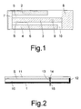
- FIG. 1 shows an antenna according to the invention with a film-like low dielectric carrier 10, which is one-sided with a conductive structure S consisting of parallel to each other and rectilinear conductor sections 2, 3 and 4 of different lengths coated is, the conductor section 3 is conductive and one-sided is connected to a ground plane 8, which in turn, as shown in Figure 2, via a conductive coating the cross-sectional area of the carrier substrate 10 is connected to ground level 1.
- the ground surface 8 by means of or a plurality of contact pins covering the dielectric substrate layer 10 reach through, with the ground level 1 in connection his.
- the conductive coating of the Cross-sectional area of the carrier substrate 10 does not have to have the entire width of the antenna, but it can be a partial coating of the film cross-sectional area made become.
- the conductor sections 2, 3 and 4 are each by a gap 5.6 of defined spa width from one another arranged separately, the conductor sections 2, 3 and 4 in each case by a strip-shaped strip running in the transverse direction Conductor section 7 of defined section length and -Width are conductively interconnected, the in Conductor section running transversely on that of the ground contact 8 opposite end of the conductor section Antenna is arranged.
- the input impedance of the microstrip array is along the location of the coupling 9 the line of symmetry of the conductor section 3 determines the again from the resulting length of the conductor sections 2 and 4 depends, the signal coupling in and out on Location 9 via a circular coaxial orifice slit or rectangular aperture.
- Dielectric constant as well as defined geometry is influenced or minimized.
- the dielectric carrier layer 10 is in particular one Polystyrene film with a layer thickness of 1 mm, which is one-sided and all over with a copper or aluminum foil Layer thickness between 0.01 mm and 0.5 mm is provided forms the ground plane.
- the dielectric layer 11 also has one Layer thickness of approx. 1 mm.
- the antenna has a length L A of 119 mm and a width B A of 40 mm.
- the length L 8 of the ground surface 8 is 20 mm.
- the distance L 5 from the ground surface 8 to the feed point of the antenna 9 is also 20 mm.
- the diameter of the aperture 15 is 4.1 mm.
- the length of the conductor sections K 1 and K 2 forming the final capacitance are 82.6 mm and 56.7 mm.
- the length L A of the conductor section 3 or R forming the resonator is 85.7 mm.
- the width of the conductor section 2 is 11.5 mm and the width of the conductor section 4 is 9.5 mm.
- the width of the resonator conductor section is 12 mm.
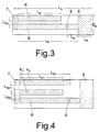
- FIG. 3 shows a radiator according to the invention, in which only one parallel to the resonator conductor section 3 or R arranged conductor section K forms the final capacitance.
- FIG. 4 shows an emitter according to the invention, in which the. Sndcapacitance is formed by two parallel conductor sections K 1 and K 2 , which are arranged on one side of the resonator conductor section R.
- an antenna can be configured in which the resulting end capacitance is realized by three or four conductor sections K 1 to K 4 .
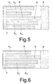
- FIG. 7 shows a further embodiment of the invention Antenna where the end capacitance is Conductor sections 16 and 17 are not rectilinear, but have a rectangular shape.
- FIG. 8 shows antennas in which the frequency bandwidth the antenna through electromagnetic coupling with additional conductor elements, which on the same dielectric carrier substrate are arranged, is adjusted or enlarged.
- the antenna according to FIG. 8 corresponds in its basic structure to the antenna according to FIG. 3, a U-shaped conductor section 19, 20, 21 with its one leg 21 in the gap between the resonator conductor section 3 and the final capacity. Head section 2 engages.
- the other leg 19 is with an additional ground surface 18 in connection, which in turn corresponding to the ground plane 9 with the ground plane i is connected.
- the basic structure of FIG. 9 corresponds of Figure 1, with two additional U-shaped Conductor sections 23 to 28 are provided, which each with its one leg 27, 28 in the through the Intervene conductor sections 2, R, 4 formed column.
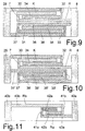
- FIGS. 9 and 10 show further possible configurations the antenna according to the invention, the arrangement of the additional, the coupling to increase the frequency bandwidths influencing conductor sections 30 to 38 is in principle arbitrary. It is also conceivable that the Interconnect conductor sections spirally so that on relatively small space a long parallel routing of conductor sections is produced.
- FIGS. 11 to 14 show antennas in which two antenna signals can be coupled in or out, as a result of which two frequency bands can be received or operated simultaneously using only one film antenna. Due to the different design of the resonator conductor sections R a and R b , the resonance conditions in connection with the conductor sections 41a, b and 42a, b and the locations 43a, 43b of the coupling-out of the electromagnetic waves are determined. Due to the nesting of the two radiator arrangements, they can be arranged in a confined space.
- FIG. 12 shows a further embodiment of an antenna with two connections 51a, 51b for dielectric waveguides, only that shown in Figure 8 Spotlight arrangement in different dimensions arranged side by side on a substrate carrier are.
- Figures 13 and 14 show a multi-layer antenna, at which the antennas according to the invention one above the other in several layers are sandwiched, one each Antenna the vibration conditions for the frequencies of a corresponds to certain cellular network. Because of the different Resonance frequencies interfere with one another arranged strahiunas structures only insignificantly. Compared to the arrangement according to FIG. 2, the Layering the radiator structures less space needed, whereby the antenna according to Figure 13 more compact and thus the housing of a mobile phone that encloses it can be made relatively small.
- FIG. 14 shows the antenna according to FIG. 13 in cross section.
- the conductive coating 12a, b of the cross-sectional area of the carrier substrates 10a and 10b is conductively connected to the structured layers S A and S B.
- Such a conductive cross-sectional coating can also be provided on the opposite side, depending on the antenna design.
Landscapes
- Waveguide Aerials (AREA)
- Details Of Aerials (AREA)
- Input Circuits Of Receivers And Coupling Of Receivers And Audio Equipment (AREA)
- Control Of Motors That Do Not Use Commutators (AREA)
- Burglar Alarm Systems (AREA)
Applications Claiming Priority (3)
| Application Number | Priority Date | Filing Date | Title |
|---|---|---|---|
| DE19707535 | 1997-02-25 | ||
| DE19707535A DE19707535A1 (de) | 1997-02-25 | 1997-02-25 | Folienstrahler |
| PCT/EP1998/001040 WO1998038694A1 (de) | 1997-02-25 | 1998-02-24 | Resonanzantenne |
Publications (2)
| Publication Number | Publication Date |
|---|---|
| EP0965152A1 EP0965152A1 (de) | 1999-12-22 |
| EP0965152B1 true EP0965152B1 (de) | 2002-09-04 |
Family
ID=7821434
Family Applications (1)
| Application Number | Title | Priority Date | Filing Date |
|---|---|---|---|
| EP98912379A Expired - Lifetime EP0965152B1 (de) | 1997-02-25 | 1998-02-24 | Resonanzantenne |
Country Status (10)
| Country | Link |
|---|---|
| US (1) | US6304219B1 (ko) |
| EP (1) | EP0965152B1 (ko) |
| JP (1) | JP2001513283A (ko) |
| KR (1) | KR20000075673A (ko) |
| AT (1) | ATE223621T1 (ko) |
| AU (1) | AU6724398A (ko) |
| CA (1) | CA2282611C (ko) |
| DE (3) | DE19707535A1 (ko) |
| IL (1) | IL131558A0 (ko) |
| WO (1) | WO1998038694A1 (ko) |
Families Citing this family (41)
| Publication number | Priority date | Publication date | Assignee | Title |
|---|---|---|---|---|
| US6343208B1 (en) * | 1998-12-16 | 2002-01-29 | Telefonaktiebolaget Lm Ericsson (Publ) | Printed multi-band patch antenna |
| FI112982B (fi) | 1999-08-25 | 2004-02-13 | Filtronic Lk Oy | Tasoantennirakenne |
| US6408190B1 (en) * | 1999-09-01 | 2002-06-18 | Telefonaktiebolaget Lm Ericsson (Publ) | Semi built-in multi-band printed antenna |
| FI114587B (fi) * | 1999-09-10 | 2004-11-15 | Filtronic Lk Oy | Tasoantennirakenne |
| DE19961488A1 (de) | 1999-12-20 | 2001-06-21 | Siemens Ag | Antenne für ein Kommunikationsendgerät |
| US20010050643A1 (en) * | 2000-02-22 | 2001-12-13 | Igor Egorov | Small-size broad-band printed antenna with parasitic element |
| FI114254B (fi) | 2000-02-24 | 2004-09-15 | Filtronic Lk Oy | Tasoantennirakenne |
| JP3658639B2 (ja) * | 2000-04-11 | 2005-06-08 | 株式会社村田製作所 | 表面実装型アンテナおよびそのアンテナを備えた無線機 |
| DE10022107A1 (de) * | 2000-05-08 | 2001-11-15 | Alcatel Sa | Integrierte Antenne für Mobilfunktelefone |
| ES2185463B1 (es) * | 2000-11-10 | 2004-09-16 | Universidad Politecnica De Cartagena | Antena dual para terminales moviles. |
| WO2002078123A1 (en) * | 2001-03-23 | 2002-10-03 | Telefonaktiebolaget L M Ericsson (Publ) | A built-in, multi band, multi antenna system |
| US6456243B1 (en) * | 2001-06-26 | 2002-09-24 | Ethertronics, Inc. | Multi frequency magnetic dipole antenna structures and methods of reusing the volume of an antenna |
| EP1439606B1 (en) * | 2001-10-11 | 2006-06-14 | Taiyo Yuden Co., Ltd. | Dielectric antenna |
| JP2003188637A (ja) * | 2001-12-20 | 2003-07-04 | Hitachi Cable Ltd | 平板多重アンテナおよび携帯端末 |
| KR20030078448A (ko) * | 2002-03-29 | 2003-10-08 | 현우마이크로 주식회사 | 아이엠티-2000(IMT-2000) 소형 중계기용 광대역 이슬롯(E-shaped SloT) 패치 안테나 |
| JP2003347827A (ja) * | 2002-05-28 | 2003-12-05 | Ngk Spark Plug Co Ltd | アンテナ及びそれを備えた無線周波モジュール |
| TWI281782B (en) * | 2002-12-25 | 2007-05-21 | Quanta Comp Inc | Portable wireless device |
| US6850199B2 (en) * | 2003-06-11 | 2005-02-01 | Auden Techno Corp. | U-shaped multi-frequency antenna of high efficiency |
| KR100623683B1 (ko) * | 2003-12-13 | 2006-09-18 | 학교법인 한국정보통신학원 | 다중대역 케이블 안테나 |
| KR100675383B1 (ko) | 2004-01-05 | 2007-01-29 | 삼성전자주식회사 | 극소형 초광대역 마이크로스트립 안테나 |
| DE102004016157A1 (de) * | 2004-04-01 | 2005-11-03 | Kathrein-Werke Kg | Antenne nach planarer Bauart |
| JP2006140589A (ja) * | 2004-11-10 | 2006-06-01 | Casio Hitachi Mobile Communications Co Ltd | アンテナ構造 |
| TWI256173B (en) | 2005-04-18 | 2006-06-01 | Wistron Neweb Corp | Planar monopole antenna |
| CN1855625A (zh) * | 2005-04-20 | 2006-11-01 | 启碁科技股份有限公司 | 平面式单极天线 |
| US7535005B2 (en) * | 2007-01-31 | 2009-05-19 | Emcore Corporation | Pulsed terahertz spectrometer |
| US7439511B2 (en) * | 2007-01-31 | 2008-10-21 | Emcore Corporation | Pulsed terahertz frequency domain spectrometer with single mode-locked laser and dispersive phase modulator |
| US7936453B2 (en) * | 2008-04-04 | 2011-05-03 | Emcore Corporation | Terahertz frequency domain spectrometer with integrated dual laser module |
| US8604433B2 (en) | 2008-05-19 | 2013-12-10 | Emcore Corporation | Terahertz frequency domain spectrometer with frequency shifting of source laser beam |
| US9029775B2 (en) | 2008-05-19 | 2015-05-12 | Joseph R. Demers | Terahertz frequency domain spectrometer with phase modulation of source laser beam |
| US7781736B2 (en) * | 2008-05-19 | 2010-08-24 | Emcore Corporation | Terahertz frequency domain spectrometer with controllable phase shift |
| TWI369816B (en) * | 2009-07-24 | 2012-08-01 | Acer Inc | Shorted monopole antenna |
| US9400214B1 (en) | 2013-03-15 | 2016-07-26 | Joseph R. Demers | Terahertz frequency domain spectrometer with a single photoconductive element for terahertz signal generation and detection |
| US9103715B1 (en) | 2013-03-15 | 2015-08-11 | Joseph R. Demers | Terahertz spectrometer phase modulator control using second harmonic nulling |
| EP2806497B1 (en) * | 2013-05-23 | 2015-12-30 | Nxp B.V. | Vehicle antenna |
| US9086374B1 (en) | 2014-04-25 | 2015-07-21 | Joseph R. Demers | Terahertz spectrometer with phase modulation and method |
| US9404853B1 (en) | 2014-04-25 | 2016-08-02 | Joseph R. Demers | Terahertz spectrometer with phase modulation |
| US9239264B1 (en) | 2014-09-18 | 2016-01-19 | Joseph R. Demers | Transceiver method and apparatus having phase modulation and common mode phase drift rejection |
| US9429473B2 (en) | 2014-10-16 | 2016-08-30 | Joseph R. Demers | Terahertz spectrometer and method for reducing photomixing interference pattern |
| US10206649B2 (en) * | 2015-12-29 | 2019-02-19 | Analogic Corporation | Data transfer across a rotating boundary of a computed tomography imaging apparatus |
| CA3140866A1 (en) | 2019-05-17 | 2020-11-26 | Aclara Technologies Llc | Multiband circular polarized antenna arrangement |
| TWI897765B (zh) * | 2024-12-13 | 2025-09-11 | 智易科技股份有限公司 | 天線裝置 |
Family Cites Families (10)
| Publication number | Priority date | Publication date | Assignee | Title |
|---|---|---|---|---|
| US5075691A (en) | 1989-07-24 | 1991-12-24 | Motorola, Inc. | Multi-resonant laminar antenna |
| DE4113277C2 (de) * | 1991-04-19 | 1996-08-08 | Hagenuk Telecom Gmbh | Antenne für ein mobiles Telefon |
| DE4121333A1 (de) * | 1991-06-25 | 1993-01-14 | Hagenuk Telecom Gmbh | Folienantenne |
| US5663639A (en) * | 1994-01-18 | 1997-09-02 | Massachusetts Institute Of Technology | Apparatus and method for optical heterodyne conversion |
| FR2718292B1 (fr) * | 1994-04-01 | 1996-06-28 | Christian Sabatier | Antenne d'émission et/ou de réception de signaux électromagnétiques, en particulier hyperfréquences, et dispositif utilisant une telle antenne. |
| DE19610806A1 (de) | 1995-03-20 | 1996-10-10 | Hitachi Media Electron Kk | Oberflächenwellen-Filter und Antennenweiche |
| US5748149A (en) * | 1995-10-04 | 1998-05-05 | Murata Manufacturing Co., Ltd. | Surface mounting antenna and antenna apparatus |
| JP3114605B2 (ja) * | 1996-02-14 | 2000-12-04 | 株式会社村田製作所 | 表面実装型アンテナおよびこれを用いた通信機 |
| US6008762A (en) * | 1997-03-31 | 1999-12-28 | Qualcomm Incorporated | Folded quarter-wave patch antenna |
| US6049314A (en) * | 1998-11-17 | 2000-04-11 | Xertex Technologies, Inc. | Wide band antenna having unitary radiator/ground plane |
-
1997
- 1997-02-25 DE DE19707535A patent/DE19707535A1/de not_active Withdrawn
-
1998
- 1998-02-24 AU AU67243/98A patent/AU6724398A/en not_active Abandoned
- 1998-02-24 AT AT98912379T patent/ATE223621T1/de not_active IP Right Cessation
- 1998-02-24 CA CA002282611A patent/CA2282611C/en not_active Expired - Fee Related
- 1998-02-24 JP JP53729098A patent/JP2001513283A/ja active Pending
- 1998-02-24 DE DE19880222T patent/DE19880222D2/de not_active Expired - Fee Related
- 1998-02-24 DE DE59805415T patent/DE59805415D1/de not_active Expired - Lifetime
- 1998-02-24 IL IL13155898A patent/IL131558A0/xx unknown
- 1998-02-24 EP EP98912379A patent/EP0965152B1/de not_active Expired - Lifetime
- 1998-02-24 KR KR1019997007739A patent/KR20000075673A/ko not_active Withdrawn
- 1998-02-24 US US09/380,131 patent/US6304219B1/en not_active Expired - Fee Related
- 1998-02-24 WO PCT/EP1998/001040 patent/WO1998038694A1/de not_active Ceased
Also Published As
| Publication number | Publication date |
|---|---|
| IL131558A0 (en) | 2001-01-28 |
| CA2282611A1 (en) | 1998-09-03 |
| DE19707535A1 (de) | 1998-08-27 |
| ATE223621T1 (de) | 2002-09-15 |
| AU6724398A (en) | 1998-09-18 |
| JP2001513283A (ja) | 2001-08-28 |
| CA2282611C (en) | 2005-11-15 |
| DE19880222D2 (de) | 2000-06-15 |
| DE59805415D1 (de) | 2002-10-10 |
| KR20000075673A (ko) | 2000-12-26 |
| WO1998038694A1 (de) | 1998-09-03 |
| EP0965152A1 (de) | 1999-12-22 |
| US6304219B1 (en) | 2001-10-16 |
Similar Documents
| Publication | Publication Date | Title |
|---|---|---|
| EP0965152B1 (de) | Resonanzantenne | |
| DE112016004868B4 (de) | Millimeterwellenantenne und diese verwendender Millimeterwellensensor | |
| DE102017103161B4 (de) | Antennenvorrichtung und Antennenarray | |
| DE69936657T2 (de) | Zirkularpolarisierte dielektrische resonatorantenne | |
| EP0952625B1 (de) | Antenne für mehrere Funkdienste | |
| DE69804023T2 (de) | Antenne | |
| EP1239543B1 (de) | Flachantenne für die mobile Satellitenkommunikation | |
| DE69608132T2 (de) | Schlitzspiralantenne mit integrierter symmetriereinrichtung und integrierter zuleitung | |
| DE102005008063B4 (de) | Antenne | |
| DE69835246T2 (de) | Doppelresonanzantennenstruktur für mehrere Frequenzbereiche | |
| EP3440738B1 (de) | Antennenvorrichtung | |
| DE60213902T2 (de) | M-förmige Antenne | |
| DE102005015561A1 (de) | Interne Breitbandantenne | |
| EP1138097A1 (de) | Halfloop-antenne | |
| DE10049844A1 (de) | Miniaturisierte Mikrowellenantenne | |
| DE10297569T5 (de) | Abgestimmte Schlitzantenne mit Hochfrequenz-MEMS und Verfahren zu deren Herstellung | |
| DE19713929A1 (de) | Sende-Empfangs-Einrichtung | |
| DE10350034A1 (de) | Antennenanordnung insbesondere für Radaranwendungen bei Kraftfahrzeugen | |
| DE102012014913A1 (de) | Elektrisch kleiner Strahler für vertikal polarisierte Funksignale | |
| DE10113349A1 (de) | Antenne mit Substrat und Leiterbahnstruktur | |
| DE60105447T2 (de) | Gedruckte patch-antenne | |
| EP1769564B1 (de) | Vorrichtung und verfahren zum senden/empfangen elektromagnetischer hf-signale | |
| DE102011117690B3 (de) | Patch-Strahler | |
| WO2004102742A1 (de) | Mehrbandfähige antenne | |
| EP3707775B1 (de) | Ein- und auskopplungsvorrichtung zwischen einem schaltungsträger und einem wellenleiter |
Legal Events
| Date | Code | Title | Description |
|---|---|---|---|
| PUAI | Public reference made under article 153(3) epc to a published international application that has entered the european phase |
Free format text: ORIGINAL CODE: 0009012 |
|
| 17P | Request for examination filed |
Effective date: 19990831 |
|
| AK | Designated contracting states |
Kind code of ref document: A1 Designated state(s): AT BE CH DE DK ES FI FR GB GR IE IT LI LU MC NL PT SE |
|
| AX | Request for extension of the european patent |
Free format text: LT PAYMENT 19990831;LV PAYMENT 19990831;MK PAYMENT 19990831;RO PAYMENT 19990831;SI PAYMENT 19990831 |
|
| GRAG | Despatch of communication of intention to grant |
Free format text: ORIGINAL CODE: EPIDOS AGRA |
|
| 17Q | First examination report despatched |
Effective date: 20010425 |
|
| GRAG | Despatch of communication of intention to grant |
Free format text: ORIGINAL CODE: EPIDOS AGRA |
|
| GRAH | Despatch of communication of intention to grant a patent |
Free format text: ORIGINAL CODE: EPIDOS IGRA |
|
| GRAH | Despatch of communication of intention to grant a patent |
Free format text: ORIGINAL CODE: EPIDOS IGRA |
|
| GRAH | Despatch of communication of intention to grant a patent |
Free format text: ORIGINAL CODE: EPIDOS IGRA |
|
| GRAA | (expected) grant |
Free format text: ORIGINAL CODE: 0009210 |
|
| AK | Designated contracting states |
Kind code of ref document: B1 Designated state(s): AT BE CH DE DK ES FI FR GB GR IE IT LI LU MC NL PT SE |
|
| AX | Request for extension of the european patent |
Free format text: LT PAYMENT 19990831;LV PAYMENT 19990831;MK PAYMENT 19990831;RO PAYMENT 19990831;SI PAYMENT 19990831 |
|
| PG25 | Lapsed in a contracting state [announced via postgrant information from national office to epo] |
Ref country code: NL Free format text: LAPSE BECAUSE OF FAILURE TO SUBMIT A TRANSLATION OF THE DESCRIPTION OR TO PAY THE FEE WITHIN THE PRESCRIBED TIME-LIMIT Effective date: 20020904 Ref country code: IT Free format text: LAPSE BECAUSE OF FAILURE TO SUBMIT A TRANSLATION OF THE DESCRIPTION OR TO PAY THE FEE WITHIN THE PRE;WARNING: LAPSES OF ITALIAN PATENTS WITH EFFECTIVE DATE BEFORE 2007 MAY HAVE OCCURRED AT ANY TIME BEFORE 2007. THE CORRECT EFFECTIVE DATE MAY BE DIFFERENT FROM THE ONE RECORDED.SCRIBED TIME-LIMIT Effective date: 20020904 Ref country code: IE Free format text: LAPSE BECAUSE OF FAILURE TO SUBMIT A TRANSLATION OF THE DESCRIPTION OR TO PAY THE FEE WITHIN THE PRESCRIBED TIME-LIMIT Effective date: 20020904 Ref country code: GR Free format text: LAPSE BECAUSE OF FAILURE TO SUBMIT A TRANSLATION OF THE DESCRIPTION OR TO PAY THE FEE WITHIN THE PRESCRIBED TIME-LIMIT Effective date: 20020904 Ref country code: FI Free format text: LAPSE BECAUSE OF FAILURE TO SUBMIT A TRANSLATION OF THE DESCRIPTION OR TO PAY THE FEE WITHIN THE PRESCRIBED TIME-LIMIT Effective date: 20020904 |
|
| REF | Corresponds to: |
Ref document number: 223621 Country of ref document: AT Date of ref document: 20020915 Kind code of ref document: T |
|
| REG | Reference to a national code |
Ref country code: GB Ref legal event code: FG4D Free format text: NOT ENGLISH |
|
| REG | Reference to a national code |
Ref country code: CH Ref legal event code: EP |
|
| REG | Reference to a national code |
Ref country code: IE Ref legal event code: FG4D Free format text: GERMAN |
|
| REF | Corresponds to: |
Ref document number: 59805415 Country of ref document: DE Date of ref document: 20021010 |
|
| PG25 | Lapsed in a contracting state [announced via postgrant information from national office to epo] |
Ref country code: SE Free format text: LAPSE BECAUSE OF FAILURE TO SUBMIT A TRANSLATION OF THE DESCRIPTION OR TO PAY THE FEE WITHIN THE PRESCRIBED TIME-LIMIT Effective date: 20021204 Ref country code: DK Free format text: LAPSE BECAUSE OF FAILURE TO SUBMIT A TRANSLATION OF THE DESCRIPTION OR TO PAY THE FEE WITHIN THE PRESCRIBED TIME-LIMIT Effective date: 20021204 |
|
| PG25 | Lapsed in a contracting state [announced via postgrant information from national office to epo] |
Ref country code: PT Free format text: LAPSE BECAUSE OF FAILURE TO SUBMIT A TRANSLATION OF THE DESCRIPTION OR TO PAY THE FEE WITHIN THE PRESCRIBED TIME-LIMIT Effective date: 20021213 |
|
| GBT | Gb: translation of ep patent filed (gb section 77(6)(a)/1977) |
Effective date: 20021219 |
|
| NLV1 | Nl: lapsed or annulled due to failure to fulfill the requirements of art. 29p and 29m of the patents act | ||
| PG25 | Lapsed in a contracting state [announced via postgrant information from national office to epo] |
Ref country code: LU Free format text: LAPSE BECAUSE OF NON-PAYMENT OF DUE FEES Effective date: 20030224 Ref country code: AT Free format text: LAPSE BECAUSE OF NON-PAYMENT OF DUE FEES Effective date: 20030224 |
|
| LTIE | Lt: invalidation of european patent or patent extension |
Effective date: 20020904 |
|
| PG25 | Lapsed in a contracting state [announced via postgrant information from national office to epo] |
Ref country code: MC Free format text: LAPSE BECAUSE OF NON-PAYMENT OF DUE FEES Effective date: 20030228 Ref country code: LI Free format text: LAPSE BECAUSE OF NON-PAYMENT OF DUE FEES Effective date: 20030228 Ref country code: CH Free format text: LAPSE BECAUSE OF NON-PAYMENT OF DUE FEES Effective date: 20030228 Ref country code: BE Free format text: LAPSE BECAUSE OF NON-PAYMENT OF DUE FEES Effective date: 20030228 |
|
| PG25 | Lapsed in a contracting state [announced via postgrant information from national office to epo] |
Ref country code: ES Free format text: LAPSE BECAUSE OF FAILURE TO SUBMIT A TRANSLATION OF THE DESCRIPTION OR TO PAY THE FEE WITHIN THE PRESCRIBED TIME-LIMIT Effective date: 20030328 |
|
| ET | Fr: translation filed | ||
| REG | Reference to a national code |
Ref country code: IE Ref legal event code: FD4D Ref document number: 0965152E Country of ref document: IE |
|
| PLBE | No opposition filed within time limit |
Free format text: ORIGINAL CODE: 0009261 |
|
| STAA | Information on the status of an ep patent application or granted ep patent |
Free format text: STATUS: NO OPPOSITION FILED WITHIN TIME LIMIT |
|
| 26N | No opposition filed |
Effective date: 20030605 |
|
| REG | Reference to a national code |
Ref country code: CH Ref legal event code: PL |
|
| PGFP | Annual fee paid to national office [announced via postgrant information from national office to epo] |
Ref country code: FR Payment date: 20060719 Year of fee payment: 9 |
|
| REG | Reference to a national code |
Ref country code: FR Ref legal event code: ST Effective date: 20071030 |
|
| PG25 | Lapsed in a contracting state [announced via postgrant information from national office to epo] |
Ref country code: FR Free format text: LAPSE BECAUSE OF NON-PAYMENT OF DUE FEES Effective date: 20070228 |
|
| PGFP | Annual fee paid to national office [announced via postgrant information from national office to epo] |
Ref country code: DE Payment date: 20120227 Year of fee payment: 15 |
|
| PGFP | Annual fee paid to national office [announced via postgrant information from national office to epo] |
Ref country code: GB Payment date: 20120208 Year of fee payment: 15 |
|
| GBPC | Gb: european patent ceased through non-payment of renewal fee |
Effective date: 20130224 |
|
| REG | Reference to a national code |
Ref country code: DE Ref legal event code: R119 Ref document number: 59805415 Country of ref document: DE Effective date: 20130903 |
|
| PG25 | Lapsed in a contracting state [announced via postgrant information from national office to epo] |
Ref country code: GB Free format text: LAPSE BECAUSE OF NON-PAYMENT OF DUE FEES Effective date: 20130224 Ref country code: DE Free format text: LAPSE BECAUSE OF NON-PAYMENT OF DUE FEES Effective date: 20130903 |