EP0965141B1 - Method of providing a gettering scheme in the manufacture of silicon-on-insulator (soi) integrated circuits - Google Patents
Method of providing a gettering scheme in the manufacture of silicon-on-insulator (soi) integrated circuits Download PDFInfo
- Publication number
- EP0965141B1 EP0965141B1 EP98944161A EP98944161A EP0965141B1 EP 0965141 B1 EP0965141 B1 EP 0965141B1 EP 98944161 A EP98944161 A EP 98944161A EP 98944161 A EP98944161 A EP 98944161A EP 0965141 B1 EP0965141 B1 EP 0965141B1
- Authority
- EP
- European Patent Office
- Prior art keywords
- silicon
- gettering
- providing
- mesas
- sunken
- Prior art date
- Legal status (The legal status is an assumption and is not a legal conclusion. Google has not performed a legal analysis and makes no representation as to the accuracy of the status listed.)
- Expired - Lifetime
Links
Images
Classifications
-
- H—ELECTRICITY
- H01—ELECTRIC ELEMENTS
- H01L—SEMICONDUCTOR DEVICES NOT COVERED BY CLASS H10
- H01L21/00—Processes or apparatus adapted for the manufacture or treatment of semiconductor or solid state devices or of parts thereof
- H01L21/70—Manufacture or treatment of devices consisting of a plurality of solid state components formed in or on a common substrate or of parts thereof; Manufacture of integrated circuit devices or of parts thereof
- H01L21/71—Manufacture of specific parts of devices defined in group H01L21/70
- H01L21/76—Making of isolation regions between components
- H01L21/762—Dielectric regions, e.g. EPIC dielectric isolation, LOCOS; Trench refilling techniques, SOI technology, use of channel stoppers
- H01L21/7624—Dielectric regions, e.g. EPIC dielectric isolation, LOCOS; Trench refilling techniques, SOI technology, use of channel stoppers using semiconductor on insulator [SOI] technology
-
- H—ELECTRICITY
- H01—ELECTRIC ELEMENTS
- H01L—SEMICONDUCTOR DEVICES NOT COVERED BY CLASS H10
- H01L21/00—Processes or apparatus adapted for the manufacture or treatment of semiconductor or solid state devices or of parts thereof
- H01L21/02—Manufacture or treatment of semiconductor devices or of parts thereof
- H01L21/04—Manufacture or treatment of semiconductor devices or of parts thereof the devices having potential barriers, e.g. a PN junction, depletion layer or carrier concentration layer
- H01L21/18—Manufacture or treatment of semiconductor devices or of parts thereof the devices having potential barriers, e.g. a PN junction, depletion layer or carrier concentration layer the devices having semiconductor bodies comprising elements of Group IV of the Periodic Table or AIIIBV compounds with or without impurities, e.g. doping materials
- H01L21/30—Treatment of semiconductor bodies using processes or apparatus not provided for in groups H01L21/20 - H01L21/26
- H01L21/322—Treatment of semiconductor bodies using processes or apparatus not provided for in groups H01L21/20 - H01L21/26 to modify their internal properties, e.g. to produce internal imperfections
- H01L21/3221—Treatment of semiconductor bodies using processes or apparatus not provided for in groups H01L21/20 - H01L21/26 to modify their internal properties, e.g. to produce internal imperfections of silicon bodies, e.g. for gettering
- H01L21/3226—Treatment of semiconductor bodies using processes or apparatus not provided for in groups H01L21/20 - H01L21/26 to modify their internal properties, e.g. to produce internal imperfections of silicon bodies, e.g. for gettering of silicon on insulator
Definitions
- the invention is in the field of Semiconductor-On-Insulator (SOI) technology, and relates more particularly to a method of providing a gettering scheme in the manufacture of SOI integrated circuits.
- SOI Semiconductor-On-Insulator
- Gettering which uses specific techniques to prevent impurities or contaminants from reaching the active regions of integrated circuits, is a well-known technique for conventional semiconductor devices fabricated using conventional bulk silicon technology.
- Two representative techniques suitable for use in bulk silicon gettering are the use of polysilicon in direct contact with the back of the substrate wafer, and the use of phosphorus doping of contact layers to obtain topside gettering of diffused impurities or contaminants.
- one of the final process steps is to dice the wafer into individual die, each of which is packaged and provided with appropriate connections to form a completed integrated circuit.
- the wafer is divided up, such as by sawing, along portions of the wafer commonly referred to as dicing rails, saw lanes or scribe lanes.
- dicing rails portions of the wafer commonly referred to as dicing rails, saw lanes or scribe lanes.
- this dicing step is performed on SOI wafers in the prior art, the interface between the SOI layer and the underlying buried oxide layer on which it is formed is left unpassivated, and thus susceptible to diffusion of contaminants or impurities resulting from cutting, packaging and/or aging.
- the interface between the active SOI layer and the underlying buried oxide since several metallic ion impurity species will diffuse readily along this interface.
- US5646053 discloses a sacrificial gettering layer which is disposed on a semiconductor material. After annealing to induce gettering, the layer is removed by CMP. US5597766, US4610079 concern techniques to separate SOI chip circuits.
- these objects are achieved by a method of the type described above in which a gettering material is provided in scribe lanes along which the SOI wafer is to be diced to obtain the individual SOI integrated circuits, and then the SOI wafer is diced along the scribe lanes, leaving a portion of the gettering material on diced edges of the individual integrated circuits.
- the gettering material is formed by oxidizing at least a portion of the silicon of the SOI wafer in the scribe lanes prior to dicing the SOI wafer along the scribe lanes.
- a portion of the silicon of the SOI wafer in the scribe lanes is oxidized to form a pattern of sunken silicon mesas which are separated by regions of oxidized silicon.
- sunken (with respect to the oxide) mesas may be formed of undoped silicon or doped silicon, and may also contain regions of different conductivity types in order to more effectively getter different species of impurities.
- At least some of the sunken mesas may form elongated conductive tracks which can be connected to a source of potential.
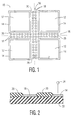
- a portion of an SOI wafer 10 is shown in simplified form in Fig. 1.
- the SOI wafer contains a plurality of integrated circuits 12, four of which are shown in the figure, although it will be recognized that the wafer will in practice contain a larger number of integrated circuits.
- Each integrated circuit may be surrounded by a potential reference lane 14, which can be connected to ground or some other fixed potential in the fmished integrated circuit.
- the wafer is diced, typically by sawing, along scribe lanes 16.
- the method of the present invention provides a gettering material in the scribe lanes 16, and then provides for dicing the SOI wafer along the scribe lanes, leaving a portion of the gettering material on diced edges of the individual integrated circuits.
- gettering is achieved by providing a plurality of silicon mesas 18, separated by regions 20 of oxidized silicon.
- a grid or pattern of sunken silicon mesas 18 separated by regions 20 of oxidized silicon are formed.
- the oxidation process causes strain fields associated with the volume expansion due to the oxidation of silicon and strain fields associated with differential thermal expansion are also created.
- strain fields are strongest along the interfaces between the SOI material 18 and the oxidized silicon regions 20, and the invention uses the principle that such strain fields can serve as highly-effective traps for mobile impurities and contaminants, thus providing effective gettering sites for such contaminants and impurities which can diffuse from the scribe lane cut areas.
- Fig. 1 shows a simplified representation of the method of the invention, for purposes of illustration, it should be understood that the method of the invention is not limited to the embodiment or configuration shown.
- the number, shape and position of the silicon mesas, the width of the scribe lanes, the spacing of the mesas, and the like can all be varied to suit particular design requirements.
- the scribe lanes 16 can be about 60-160 microns wide, or about one or two times the width of a typical saw blade.
- a representative size for the sunken silicon mesas 18 can be about 10 microns square, with a center-to-center pitch for the mesas being in the order of 20-40 microns.
- the potential reference lane 14 may have a width of about 20 microns, and, in accordance with the invention, may be provided with mesas 18 in the same manner as shown in the scribe lanes 16, although the individual mesas are not shown within the potential reference lanes for clarity and simplicity.
- FIG. 2 A simplified cross-sectional view taken along the line 2-2 in Fig. 1 is shown in Fig. 2.
- This figure shows, in simplified form, a sunken silicon mesa 18 on an insulator layer 22 and separated from other mesas by regions of oxidized silicon 20.
- a portion of the potential reference lane 14 also formed in this embodiment as a plurality of spaced sunken silicon mesas in accordance with the invention, and provided with an electrical contact, symbolically shown by the connection line designated 24.
- the regions of oxidized silicon 20 are higher than the silicon mesas 18 due to the volume expansion of silicon as a result of the oxidation process.
- the sunken silicon mesas 18 may be formed of various materials or combinations of materials.
- the mesas 18 may be formed of undoped silicon, doped silicon, or polysilicon.
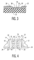
- each sunken silicon mesa 18 may be formed of at least one region of n-type silicon and at least one region of p-type silicon, as shown by regions 26 and 28 in Fig. 3, with the regions 26 and 28 forming a p-n junction 30 at their intersection.
- the configuration of Fig. 3 is more complex than that of Fig. 2, it offers the additional advantage of improved gettering, in that different contaminants preferentially segregated out to either n-type or p-type semiconductor material.
- each mesa with two regions of n-type silicon and two regions of p-type silicon in a checkerboard pattern, in which case the cross-section through a sunken silicon mesa 18 in a direction orthogonal to the direction of the cross-section of Figs. 2 and 3 (i.e., in the vertical direction in Fig. 1) would also show two regions analogous to regions 26 and 28 in Fig. 3.
- a further improvement in gettering performance may be achieved in accordance with the invention by connecting some or all of the silicon material in the scribe lanes 16 to a source of potential in order to prevent field-assisted migration of contaminant species from influencing the active regions of the integrated circuits.
- An electrical connection for providing such a source of potential to a silicon region is shown symbolically by electrical connection 24 to potential reference lane 14 in Fig. 2.
- FIG. 4 shows a portion of an SOI wafer analogous to the lower-central portion of the SOI wafer 10 shown in Fig. 1.
- portions of two integrated circuits 12 are surrounded by potential reference lanes 14, as in Fig. 1.
- the integrated circuits 12 are separated by scribe lanes 16 having a plurality of silicon mesas 18.
- the silicon mesas 18 are separated by annular, rather than continuous, regions 20 of oxidized silicon.
- the oxidized silicon regions 20 are in turn surrounded by a substantially continuous region 32 of silicon, thus providing a substantially continuous conductive path along the scribe lanes to which an electrical connection such as the electrical connection 24 in Fig. 2 may be provided so that a source of potential may be applied to the regions 32 in order to improve gettering performance.
- annular rings of oxidized silicon 34 may be formed between potential reference lanes 14 and the silicon regions 32. It will be recognized that whereas the silicon mesas 18 are of a generally square or rectangular shape, the sunken silicon regions 32 will generally be in the form of elongated silicon mesas or tracks extended in the vertical or horizontal direction when viewed from above.
- the present invention provides a gettering scheme in the manufacture of individual SOI integrated circuits from an SOI wafer containing a number of such circuits which is both simple and effective.
- doped regions within the sunken silicon mesas may be formed by implantation or diffusion, and the regions of oxidized silicon may be formed by a LOCOS technique or other suitable oxidation process.
Landscapes
- Engineering & Computer Science (AREA)
- Physics & Mathematics (AREA)
- Condensed Matter Physics & Semiconductors (AREA)
- General Physics & Mathematics (AREA)
- Manufacturing & Machinery (AREA)
- Computer Hardware Design (AREA)
- Microelectronics & Electronic Packaging (AREA)
- Power Engineering (AREA)
- Element Separation (AREA)
- Dicing (AREA)
Applications Claiming Priority (3)
| Application Number | Priority Date | Filing Date | Title |
|---|---|---|---|
| US996672 | 1997-12-23 | ||
| US08/996,672 US6093624A (en) | 1997-12-23 | 1997-12-23 | Method of providing a gettering scheme in the manufacture of silicon-on-insulator (SOI) integrated circuits |
| PCT/IB1998/001532 WO1999034432A1 (en) | 1997-12-23 | 1998-10-05 | Method of providing a gettering scheme in the manufacture of silicon-on-insulator (soi) integrated circuits |
Publications (2)
| Publication Number | Publication Date |
|---|---|
| EP0965141A1 EP0965141A1 (en) | 1999-12-22 |
| EP0965141B1 true EP0965141B1 (en) | 2006-08-09 |
Family
ID=25543175
Family Applications (1)
| Application Number | Title | Priority Date | Filing Date |
|---|---|---|---|
| EP98944161A Expired - Lifetime EP0965141B1 (en) | 1997-12-23 | 1998-10-05 | Method of providing a gettering scheme in the manufacture of silicon-on-insulator (soi) integrated circuits |
Country Status (6)
| Country | Link |
|---|---|
| US (1) | US6093624A (enExample) |
| EP (1) | EP0965141B1 (enExample) |
| JP (1) | JP4372847B2 (enExample) |
| KR (1) | KR100541539B1 (enExample) |
| DE (1) | DE69835505T2 (enExample) |
| WO (1) | WO1999034432A1 (enExample) |
Families Citing this family (23)
| Publication number | Priority date | Publication date | Assignee | Title |
|---|---|---|---|---|
| JP4573953B2 (ja) * | 2000-06-27 | 2010-11-04 | 株式会社半導体エネルギー研究所 | 半導体装置の作製方法 |
| US6498061B2 (en) * | 2000-12-06 | 2002-12-24 | International Business Machines Corporation | Negative ion implant mask formation for self-aligned, sublithographic resolution patterning for single-sided vertical device formation |
| US6383924B1 (en) * | 2000-12-13 | 2002-05-07 | Micron Technology, Inc. | Method of forming buried conductor patterns by surface transformation of empty spaces in solid state materials |
| US6444534B1 (en) | 2001-01-30 | 2002-09-03 | Advanced Micro Devices, Inc. | SOI semiconductor device opening implantation gettering method |
| US6376336B1 (en) | 2001-02-01 | 2002-04-23 | Advanced Micro Devices, Inc. | Frontside SOI gettering with phosphorus doping |
| US6670259B1 (en) | 2001-02-21 | 2003-12-30 | Advanced Micro Devices, Inc. | Inert atom implantation method for SOI gettering |
| US7142577B2 (en) * | 2001-05-16 | 2006-11-28 | Micron Technology, Inc. | Method of forming mirrors by surface transformation of empty spaces in solid state materials and structures thereon |
| US6898362B2 (en) * | 2002-01-17 | 2005-05-24 | Micron Technology Inc. | Three-dimensional photonic crystal waveguide structure and method |
| US6987037B2 (en) * | 2003-05-07 | 2006-01-17 | Micron Technology, Inc. | Strained Si/SiGe structures by ion implantation |
| US7273788B2 (en) | 2003-05-21 | 2007-09-25 | Micron Technology, Inc. | Ultra-thin semiconductors bonded on glass substrates |
| US7008854B2 (en) | 2003-05-21 | 2006-03-07 | Micron Technology, Inc. | Silicon oxycarbide substrates for bonded silicon on insulator |
| US7501329B2 (en) * | 2003-05-21 | 2009-03-10 | Micron Technology, Inc. | Wafer gettering using relaxed silicon germanium epitaxial proximity layers |
| US7662701B2 (en) * | 2003-05-21 | 2010-02-16 | Micron Technology, Inc. | Gettering of silicon on insulator using relaxed silicon germanium epitaxial proximity layers |
| US6929984B2 (en) * | 2003-07-21 | 2005-08-16 | Micron Technology Inc. | Gettering using voids formed by surface transformation |
| US7153753B2 (en) * | 2003-08-05 | 2006-12-26 | Micron Technology, Inc. | Strained Si/SiGe/SOI islands and processes of making same |
| US20050255677A1 (en) * | 2004-05-17 | 2005-11-17 | Weigold Jason W | Integrated circuit with impurity barrier |
| US20060115958A1 (en) * | 2004-11-22 | 2006-06-01 | Weigold Jason W | Method and apparatus for forming buried oxygen precipitate layers in multi-layer wafers |
| JP2006196514A (ja) * | 2005-01-11 | 2006-07-27 | Nec Electronics Corp | 半導体装置及びその製造方法 |
| TWI355046B (en) * | 2007-07-10 | 2011-12-21 | Nanya Technology Corp | Two bit memory structure and method of making the |
| US7928690B2 (en) * | 2007-11-29 | 2011-04-19 | GM Global Technology Operations LLC | Method and system for determining a state of charge of a battery |
| JP5470766B2 (ja) * | 2008-07-18 | 2014-04-16 | 株式会社Sumco | 半導体デバイスの製造方法 |
| US9231020B2 (en) | 2014-01-16 | 2016-01-05 | Tower Semiconductor Ltd. | Device and method of gettering on silicon on insulator (SOI) substrate |
| KR102399356B1 (ko) | 2017-03-10 | 2022-05-19 | 삼성전자주식회사 | 기판, 기판의 쏘잉 방법, 및 반도체 소자 |
Family Cites Families (11)
| Publication number | Priority date | Publication date | Assignee | Title |
|---|---|---|---|---|
| JPS56103447A (en) * | 1980-01-22 | 1981-08-18 | Toshiba Corp | Dicing method of semiconductor wafer |
| US5096855A (en) * | 1988-05-23 | 1992-03-17 | U.S. Philips Corporation | Method of dicing semiconductor wafers which produces shards less than 10 microns in size |
| JPH04266047A (ja) * | 1991-02-20 | 1992-09-22 | Fujitsu Ltd | 埋め込み層形成に相当するsoi型半導体装置の製造方法及び半導体装置 |
| US5244819A (en) * | 1991-10-22 | 1993-09-14 | Honeywell Inc. | Method to getter contamination in semiconductor devices |
| US5556793A (en) * | 1992-02-28 | 1996-09-17 | Motorola, Inc. | Method of making a structure for top surface gettering of metallic impurities |
| DE4317721C1 (de) * | 1993-05-27 | 1994-07-21 | Siemens Ag | Verfahren zur Vereinzelung von Chips aus einem Wafer |
| TW274628B (enExample) * | 1994-06-03 | 1996-04-21 | At & T Corp | |
| US5429981A (en) * | 1994-06-30 | 1995-07-04 | Honeywell Inc. | Method of making linear capacitors for high temperature applications |
| KR0172548B1 (ko) * | 1995-06-30 | 1999-02-01 | 김주용 | 반도체 소자 및 그 제조방법 |
| US5646053A (en) * | 1995-12-20 | 1997-07-08 | International Business Machines Corporation | Method and structure for front-side gettering of silicon-on-insulator substrates |
| US5622899A (en) * | 1996-04-22 | 1997-04-22 | Taiwan Semiconductor Manufacturing Company Ltd. | Method of fabricating semiconductor chips separated by scribe lines used for endpoint detection |
-
1997
- 1997-12-23 US US08/996,672 patent/US6093624A/en not_active Expired - Lifetime
-
1998
- 1998-10-05 DE DE69835505T patent/DE69835505T2/de not_active Expired - Lifetime
- 1998-10-05 KR KR1019997008112A patent/KR100541539B1/ko not_active Expired - Fee Related
- 1998-10-05 EP EP98944161A patent/EP0965141B1/en not_active Expired - Lifetime
- 1998-10-05 JP JP53467599A patent/JP4372847B2/ja not_active Expired - Fee Related
- 1998-10-05 WO PCT/IB1998/001532 patent/WO1999034432A1/en not_active Ceased
Also Published As
| Publication number | Publication date |
|---|---|
| EP0965141A1 (en) | 1999-12-22 |
| DE69835505T2 (de) | 2007-04-05 |
| KR20000076026A (ko) | 2000-12-26 |
| US6093624A (en) | 2000-07-25 |
| JP2001513948A (ja) | 2001-09-04 |
| WO1999034432A1 (en) | 1999-07-08 |
| DE69835505D1 (de) | 2006-09-21 |
| JP4372847B2 (ja) | 2009-11-25 |
| KR100541539B1 (ko) | 2006-01-12 |
Similar Documents
| Publication | Publication Date | Title |
|---|---|---|
| EP0965141B1 (en) | Method of providing a gettering scheme in the manufacture of silicon-on-insulator (soi) integrated circuits | |
| US5323059A (en) | Vertical current flow semiconductor device utilizing wafer bonding | |
| US4710794A (en) | Composite semiconductor device | |
| US4860081A (en) | Semiconductor integrated circuit structure with insulative partitions | |
| US6013936A (en) | Double silicon-on-insulator device and method therefor | |
| JP3292651B2 (ja) | 光起電力装置 | |
| US4835592A (en) | Semiconductor wafer with dice having briding metal structure and method of manufacturing same | |
| JPS62273736A (ja) | 半導体集積回路デバイスのための封止構造 | |
| US5541140A (en) | Semiconductor arrangement and method for its manufacture | |
| EP0323856A2 (en) | Substrate structure for composite semiconductor device | |
| EP0615287B1 (en) | Dielectric isolated bipolar transistor | |
| US4999684A (en) | Symmetrical blocking high voltage breakdown semiconducotr device | |
| US4837177A (en) | Method of making bipolar semiconductor device having a conductive recombination layer | |
| JPH1070245A (ja) | 基板から誘電的に絶縁されたデバイス及び接合絶縁されたデバイスを含む集積回路 | |
| US4046605A (en) | Method of electrically isolating individual semiconductor circuits in a wafer | |
| JP2007194622A (ja) | 面積効率の高いゲート・ダイオード構造およびこれを形成する方法 | |
| US6104078A (en) | Design for a semiconductor device having elements isolated by insulating regions | |
| US4149177A (en) | Method of fabricating conductive buried regions in integrated circuits and the resulting structures | |
| JP2009521131A (ja) | 半導体装置とその形成方法 | |
| US5789307A (en) | Method of separating electronic devices contained in a carrier | |
| JP2005183891A (ja) | 双方向ブロック型プレーナデバイスの構造と製法 | |
| JP2979554B2 (ja) | 半導体装置の製造方法 | |
| JP3942192B2 (ja) | 半導体集積回路装置およびその製造方法 | |
| JP2014508402A (ja) | Soi基板の活性層内に形成されるデバイス構造体、製造する方法、及び、集積回路の設計構造体 | |
| JP4194841B2 (ja) | 半導体装置配置 |
Legal Events
| Date | Code | Title | Description |
|---|---|---|---|
| PUAI | Public reference made under article 153(3) epc to a published international application that has entered the european phase |
Free format text: ORIGINAL CODE: 0009012 |
|
| AK | Designated contracting states |
Kind code of ref document: A1 Designated state(s): DE FR GB |
|
| 17P | Request for examination filed |
Effective date: 20000110 |
|
| GRAJ | Information related to disapproval of communication of intention to grant by the applicant or resumption of examination proceedings by the epo deleted |
Free format text: ORIGINAL CODE: EPIDOSDIGR1 |
|
| GRAP | Despatch of communication of intention to grant a patent |
Free format text: ORIGINAL CODE: EPIDOSNIGR1 |
|
| GRAP | Despatch of communication of intention to grant a patent |
Free format text: ORIGINAL CODE: EPIDOSNIGR1 |
|
| GRAS | Grant fee paid |
Free format text: ORIGINAL CODE: EPIDOSNIGR3 |
|
| GRAA | (expected) grant |
Free format text: ORIGINAL CODE: 0009210 |
|
| AK | Designated contracting states |
Kind code of ref document: B1 Designated state(s): DE FR GB |
|
| REG | Reference to a national code |
Ref country code: GB Ref legal event code: FG4D |
|
| REF | Corresponds to: |
Ref document number: 69835505 Country of ref document: DE Date of ref document: 20060921 Kind code of ref document: P |
|
| REG | Reference to a national code |
Ref country code: GB Ref legal event code: 732E |
|
| REG | Reference to a national code |
Ref country code: GB Ref legal event code: 732E |
|
| ET | Fr: translation filed | ||
| REG | Reference to a national code |
Ref country code: FR Ref legal event code: TP |
|
| PLBE | No opposition filed within time limit |
Free format text: ORIGINAL CODE: 0009261 |
|
| STAA | Information on the status of an ep patent application or granted ep patent |
Free format text: STATUS: NO OPPOSITION FILED WITHIN TIME LIMIT |
|
| 26N | No opposition filed |
Effective date: 20070510 |
|
| REG | Reference to a national code |
Ref country code: FR Ref legal event code: GC |
|
| REG | Reference to a national code |
Ref country code: FR Ref legal event code: GC |
|
| REG | Reference to a national code |
Ref country code: FR Ref legal event code: GC |
|
| REG | Reference to a national code |
Ref country code: FR Ref legal event code: AU Effective date: 20120126 |
|
| PGFP | Annual fee paid to national office [announced via postgrant information from national office to epo] |
Ref country code: GB Payment date: 20120924 Year of fee payment: 15 |
|
| REG | Reference to a national code |
Ref country code: FR Ref legal event code: AU Effective date: 20121009 |
|
| REG | Reference to a national code |
Ref country code: FR Ref legal event code: AU Effective date: 20130402 |
|
| REG | Reference to a national code |
Ref country code: GB Ref legal event code: 732E Free format text: REGISTERED BETWEEN 20130606 AND 20130612 |
|
| GBPC | Gb: european patent ceased through non-payment of renewal fee |
Effective date: 20131005 |
|
| PG25 | Lapsed in a contracting state [announced via postgrant information from national office to epo] |
Ref country code: GB Free format text: LAPSE BECAUSE OF NON-PAYMENT OF DUE FEES Effective date: 20131005 |
|
| REG | Reference to a national code |
Ref country code: FR Ref legal event code: PLFP Year of fee payment: 19 |
|
| REG | Reference to a national code |
Ref country code: FR Ref legal event code: PLFP Year of fee payment: 20 |
|
| PGFP | Annual fee paid to national office [announced via postgrant information from national office to epo] |
Ref country code: FR Payment date: 20170921 Year of fee payment: 20 |
|
| PGFP | Annual fee paid to national office [announced via postgrant information from national office to epo] |
Ref country code: DE Payment date: 20170920 Year of fee payment: 20 |
|
| REG | Reference to a national code |
Ref country code: DE Ref legal event code: R071 Ref document number: 69835505 Country of ref document: DE |