EP0964450A1 - Intergrierte Halbleiterschaltung mit einer Anschlussfläche - Google Patents
Intergrierte Halbleiterschaltung mit einer Anschlussfläche Download PDFInfo
- Publication number
- EP0964450A1 EP0964450A1 EP99106322A EP99106322A EP0964450A1 EP 0964450 A1 EP0964450 A1 EP 0964450A1 EP 99106322 A EP99106322 A EP 99106322A EP 99106322 A EP99106322 A EP 99106322A EP 0964450 A1 EP0964450 A1 EP 0964450A1
- Authority
- EP
- European Patent Office
- Prior art keywords
- doping
- semiconductor circuit
- pad
- integrated semiconductor
- polysilicon
- Prior art date
- Legal status (The legal status is an assumption and is not a legal conclusion. Google has not performed a legal analysis and makes no representation as to the accuracy of the status listed.)
- Withdrawn
Links
Images

Classifications
-
- H—ELECTRICITY
- H01—ELECTRIC ELEMENTS
- H01L—SEMICONDUCTOR DEVICES NOT COVERED BY CLASS H10
- H01L23/00—Details of semiconductor or other solid state devices
- H01L23/48—Arrangements for conducting electric current to or from the solid state body in operation, e.g. leads, terminal arrangements ; Selection of materials therefor
- H01L23/50—Arrangements for conducting electric current to or from the solid state body in operation, e.g. leads, terminal arrangements ; Selection of materials therefor for integrated circuit devices, e.g. power bus, number of leads
-
- H—ELECTRICITY
- H10—SEMICONDUCTOR DEVICES; ELECTRIC SOLID-STATE DEVICES NOT OTHERWISE PROVIDED FOR
- H10D—INORGANIC ELECTRIC SEMICONDUCTOR DEVICES
- H10D84/00—Integrated devices formed in or on semiconductor substrates that comprise only semiconducting layers, e.g. on Si wafers or on GaAs-on-Si wafers
- H10D84/201—Integrated devices formed in or on semiconductor substrates that comprise only semiconducting layers, e.g. on Si wafers or on GaAs-on-Si wafers characterised by the integration of only components covered by H10D1/00 or H10D8/00, e.g. RLC circuits
- H10D84/204—Integrated devices formed in or on semiconductor substrates that comprise only semiconducting layers, e.g. on Si wafers or on GaAs-on-Si wafers characterised by the integration of only components covered by H10D1/00 or H10D8/00, e.g. RLC circuits of combinations of diodes or capacitors or resistors
- H10D84/212—Integrated devices formed in or on semiconductor substrates that comprise only semiconducting layers, e.g. on Si wafers or on GaAs-on-Si wafers characterised by the integration of only components covered by H10D1/00 or H10D8/00, e.g. RLC circuits of combinations of diodes or capacitors or resistors of only capacitors
-
- H—ELECTRICITY
- H01—ELECTRIC ELEMENTS
- H01L—SEMICONDUCTOR DEVICES NOT COVERED BY CLASS H10
- H01L2224/00—Indexing scheme for arrangements for connecting or disconnecting semiconductor or solid-state bodies and methods related thereto as covered by H01L24/00
- H01L2224/01—Means for bonding being attached to, or being formed on, the surface to be connected, e.g. chip-to-package, die-attach, "first-level" interconnects; Manufacturing methods related thereto
- H01L2224/02—Bonding areas; Manufacturing methods related thereto
- H01L2224/04—Structure, shape, material or disposition of the bonding areas prior to the connecting process
- H01L2224/05—Structure, shape, material or disposition of the bonding areas prior to the connecting process of an individual bonding area
- H01L2224/0554—External layer
- H01L2224/05599—Material
-
- H—ELECTRICITY
- H01—ELECTRIC ELEMENTS
- H01L—SEMICONDUCTOR DEVICES NOT COVERED BY CLASS H10
- H01L2924/00—Indexing scheme for arrangements or methods for connecting or disconnecting semiconductor or solid-state bodies as covered by H01L24/00
- H01L2924/01—Chemical elements
- H01L2924/01004—Beryllium [Be]
-
- H—ELECTRICITY
- H01—ELECTRIC ELEMENTS
- H01L—SEMICONDUCTOR DEVICES NOT COVERED BY CLASS H10
- H01L2924/00—Indexing scheme for arrangements or methods for connecting or disconnecting semiconductor or solid-state bodies as covered by H01L24/00
- H01L2924/01—Chemical elements
- H01L2924/01005—Boron [B]
-
- H—ELECTRICITY
- H01—ELECTRIC ELEMENTS
- H01L—SEMICONDUCTOR DEVICES NOT COVERED BY CLASS H10
- H01L2924/00—Indexing scheme for arrangements or methods for connecting or disconnecting semiconductor or solid-state bodies as covered by H01L24/00
- H01L2924/01—Chemical elements
- H01L2924/01015—Phosphorus [P]
-
- H—ELECTRICITY
- H01—ELECTRIC ELEMENTS
- H01L—SEMICONDUCTOR DEVICES NOT COVERED BY CLASS H10
- H01L2924/00—Indexing scheme for arrangements or methods for connecting or disconnecting semiconductor or solid-state bodies as covered by H01L24/00
- H01L2924/01—Chemical elements
- H01L2924/01033—Arsenic [As]
-
- H—ELECTRICITY
- H01—ELECTRIC ELEMENTS
- H01L—SEMICONDUCTOR DEVICES NOT COVERED BY CLASS H10
- H01L2924/00—Indexing scheme for arrangements or methods for connecting or disconnecting semiconductor or solid-state bodies as covered by H01L24/00
- H01L2924/01—Chemical elements
- H01L2924/01078—Platinum [Pt]
-
- H—ELECTRICITY
- H01—ELECTRIC ELEMENTS
- H01L—SEMICONDUCTOR DEVICES NOT COVERED BY CLASS H10
- H01L2924/00—Indexing scheme for arrangements or methods for connecting or disconnecting semiconductor or solid-state bodies as covered by H01L24/00
- H01L2924/01—Chemical elements
- H01L2924/01082—Lead [Pb]
-
- H—ELECTRICITY
- H01—ELECTRIC ELEMENTS
- H01L—SEMICONDUCTOR DEVICES NOT COVERED BY CLASS H10
- H01L2924/00—Indexing scheme for arrangements or methods for connecting or disconnecting semiconductor or solid-state bodies as covered by H01L24/00
- H01L2924/10—Details of semiconductor or other solid state devices to be connected
- H01L2924/11—Device type
- H01L2924/12—Passive devices, e.g. 2 terminal devices
- H01L2924/1203—Rectifying Diode
- H01L2924/12036—PN diode
-
- H—ELECTRICITY
- H01—ELECTRIC ELEMENTS
- H01L—SEMICONDUCTOR DEVICES NOT COVERED BY CLASS H10
- H01L2924/00—Indexing scheme for arrangements or methods for connecting or disconnecting semiconductor or solid-state bodies as covered by H01L24/00
- H01L2924/10—Details of semiconductor or other solid state devices to be connected
- H01L2924/11—Device type
- H01L2924/13—Discrete devices, e.g. 3 terminal devices
- H01L2924/1304—Transistor
- H01L2924/1306—Field-effect transistor [FET]
- H01L2924/13091—Metal-Oxide-Semiconductor Field-Effect Transistor [MOSFET]
-
- H—ELECTRICITY
- H01—ELECTRIC ELEMENTS
- H01L—SEMICONDUCTOR DEVICES NOT COVERED BY CLASS H10
- H01L2924/00—Indexing scheme for arrangements or methods for connecting or disconnecting semiconductor or solid-state bodies as covered by H01L24/00
- H01L2924/10—Details of semiconductor or other solid state devices to be connected
- H01L2924/11—Device type
- H01L2924/14—Integrated circuits
-
- H—ELECTRICITY
- H01—ELECTRIC ELEMENTS
- H01L—SEMICONDUCTOR DEVICES NOT COVERED BY CLASS H10
- H01L2924/00—Indexing scheme for arrangements or methods for connecting or disconnecting semiconductor or solid-state bodies as covered by H01L24/00
- H01L2924/19—Details of hybrid assemblies other than the semiconductor or other solid state devices to be connected
- H01L2924/1901—Structure
- H01L2924/1904—Component type
- H01L2924/19041—Component type being a capacitor
-
- H—ELECTRICITY
- H01—ELECTRIC ELEMENTS
- H01L—SEMICONDUCTOR DEVICES NOT COVERED BY CLASS H10
- H01L2924/00—Indexing scheme for arrangements or methods for connecting or disconnecting semiconductor or solid-state bodies as covered by H01L24/00
- H01L2924/19—Details of hybrid assemblies other than the semiconductor or other solid state devices to be connected
- H01L2924/1901—Structure
- H01L2924/1904—Component type
- H01L2924/19043—Component type being a resistor
Definitions
- the invention relates to an integrated semiconductor circuit, which is a substrate with a doping of a first doping type includes as well as a pad for input or output of a signal to be processed or to supply a Supply potential.
- Integrated semiconductor circuits are known to have pads, so-called pads, on the pins of a housing are contacted and via which the of the Semiconductor circuit to be processed input or output signals be supplied or discharged or to which a supply potential is created.
- pads so-called pads
- the lines connected to the connection surface e.g. Bond wire, housing pin, conductor track on the circuit board, to make.
- pages 593 to 594 is one integrated circuit with a capacitance structure for decoupling the supply voltage supply described.
- the Decoupling capacitor comprises an n-well region in a p-substrate, on which a polysilicon layer separated by a thin oxide is arranged.
- One pole of the supply voltage is connected to the tub, the other to polysilicon.
- the object of the invention is an integrated Specify semiconductor circuit in which the adaptation to input / output parameters your connections with less effort is feasible.
- the structure of the neighboring doping areas is modular built up. Polysilicon tracks are advantageously above the doping regions.
- a suitable one Metallization becomes the doping areas and polysilicon traces with the pad (or pad) or the Substrate and thus the supply potential.
- a desired capacitive is then on the connection pad Load on.
- one is arranged in the connecting line Resistance trimmed to a desired value.
- the input / output time behavior of the pad becomes overall set to a desired RC constant.
- the invention Structure enables a fine gradation of the RC behavior for the connection pad in a wide setting range.
- the structure of doping areas and polysilicon areas is located in deep layers of the integrated Circuit.
- the individual wiring of the structure for Connection to the pad only affects the upper ones Layers of the circuit.
- the same basic layout can therefore for a variety of different input / output characteristics be used.
- the funding areas and polysilicon traces are in such areas of the semiconductor circuit, that of other active elements, e.g. Transistors or diodes, are not used, but preferably below the pad.
- the areas are sufficiently far from the vertical Terminal removed so that it is not damaged during bonding become.
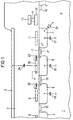
- FIG. 1 shows a weakly p - -doped semiconductor substrate 1, over which part of a connection area 3 is arranged, separated by a field oxide layer 2.
- a bonding wire is stamped on the metal pad 3 in order to make a connection with a pin which leads outside the housing.
- the pad 3 is located in the top metallization level of the semiconductor chip. Input signals to be processed by the circuit are supplied or processed output signals are output via the pad 3.
- a potential of a supply voltage can be fed in, for example a positive supply potential.
- connection pad 3 In order to achieve the best possible signal transmission, it is required, the input / output characteristics of the connection pad 3 to a desired time constant.
- This time constant depends, among other things, on the length of the Bond wire, the length and design of the pin as well as the properties of those arranged on the circuit board Lines off. Around the connections of the semiconductor circuit connect to a standardized data bus, is usually required that the time constant is within certain tolerances.
- doping regions 4, 5, 6, 7 are arranged in the semiconductor substrate 1 below the pad 3.
- the doping regions have an opposite n + doping type compared to the semiconductor substrate. They are designed as well doping regions, that is to say they have a doping that is substantially deeper than the drain and source doping regions of MOS transistors, with a dopant concentration that is about two orders of magnitude lower.
- Each doping region forms a pn junction with the substrate, of which the pn junction 24 is symbolically represented as a diode.
- Each of the doping regions 4, ..., 7 can optionally be connected to the pad 3.
- the semiconductor substrate 1 is connected to the most negative of the potentials applied to the circuit, usually to ground.
- connection pad 3 Depending on the desired capacitive load on the connection pad 3, a suitable number of doping regions is connected to the pad 3.
- the respective pn junctions between the doping region and the substrate act as capacitances 19, 20, 21.
- the connection is established via conductor tracks 13, 12 as described in connection with FIG. 2.
- a polysilicon surface 8, ..., 11 is preferably arranged above each of the doping regions 4, ..., 7.
- An oxide in the thickness of the gate oxide of a MOS transistor is formed between the polysilicon surface and the doping region.
- the oxide can also be a field oxide of greater thickness.
- some of the polysilicon areas are also connected, either to the substrate 1 or to the connection pad 3.
- the former connection is led to a substrate connection doping area 18 which surrounds the arrangement of the well doping areas and polysilicon areas.
- the part 18 of the substrate connection doping region which is visible in cross section has the same doping type compared to substrate 1, but with a significantly higher dopant concentration (p + ).
- the latter connection of the polysilicon surfaces to the pad 3 takes place via the metal conductor track 13.
- This runs in the first lower metallization level. It has a section whose resistance value is trimmed to a predetermined value in order to set the resistance component of the RC behavior.
- the resistance section is expediently formed from polysilicon.
- the metal conductor track 13 is interrupted and is bridged with the polysilicon section 12 in that the latter is connected via a contact to the interrupted parts of the metal conductor track 13, the distance between the contacts being a measure of the resistance.
- the doping regions are special in the embodiment shown in FIG 6 and 7 via the conductive connection 12, 13 connected to pad 3. Their formed against the substrate Capacities 20 and 21 are therefore effective on pad 3 connected.
- the polysilicon surface 11 is not connected.
- the Polysilicon surface 10 is connected to the substrate contact, so that one between polysilicon surface 10 and doping region 6 over the capacitance formed between the gate oxide is effective, the electrically parallel to the capacitor 20th lies.
- the folysilicon surface 9 is connected to the pad 3 via the connecting lines 12, 13.
- polysilicon area and doping area can be activated. At a large number of doping regions arranged side by side and polysilicon areas enables a very fine Capacity grading in a wide range of values.
- FIG. 2 shows a supervision of a capacity structure.
- the capacity structure is expediently below a connection pad so that no additional space is used becomes. Because the structures are covered by a thick oxide layer 2 are sufficiently far away from pad 3, the structure not damaged by stamping the bond wire.
- the capacity structure can easily be set outside of one Pads in otherwise unused active areas of the Semiconductor chips are arranged.
- the connecting lines 12, 13 are then to be managed accordingly.
- the intersection line 30 in 2 corresponds to that shown in cross section in FIG Neckline.
- the doping areas and polysilicon areas are strip-shaped, rectangular and parallel to each other.
- the connecting line 13 surrounds on three sides of the Doping areas occupied area.
- the metal conductor 13 At port 32 is contacted the metal conductor 13 to the pad upwards.
- the Metallization interrupted in the lower section 12a to 12b of the connecting line is the Metallization interrupted.
- section 33 are metal conductor tracks and metallization on top of each other.
- the resistance of the connecting line set to a predetermined value.
- the funding areas as well the overlying polysilicon areas face at their respective left margin one connection area 34 and 35 respectively, via which they can be connected.
- connection area 34 of the Doping areas can be connected to the connecting line, which continued in this section as a metal conductor track becomes.
- the connection 35 for the polysilicon surface can either connected to the trace for connection to the pad be or to the substrate. In the latter case the conductor track 35 contacts the substrate ring 18.
- the doping region 7 corresponds to FIG. 1 connected to the connecting line to the pad, which in this Section 36 is shown symbolically.
- the polysilicon area 11 is also contacted to the metal conductor track 36.
- the doping region is in the adjacent substructure 6 connected to the conductor track section 36, the polysilicon surface 10 is contacted to the substrate ring 18.
- the polysilicon surface is in turn the adjacent substructure 9 connected to the conductor track section 36, the Funding area remains unconnected.
- the connection pad 3 are possibly also shares of the other doping areas and polysilicon areas to the connecting line 36 and the latter alternatively also connected to the substrate.
- Branches 15, 16, 17 of the substrate ring 18 are arranged between the doping regions. Like the substrate ring 18, these also consist of p + -doped regions. They serve to improve the latch-up strength by sucking off charge carriers that can arise when the applied signal overshoots or undershoots on the pad.
Landscapes
- Physics & Mathematics (AREA)
- Condensed Matter Physics & Semiconductors (AREA)
- General Physics & Mathematics (AREA)
- Engineering & Computer Science (AREA)
- Computer Hardware Design (AREA)
- Microelectronics & Electronic Packaging (AREA)
- Power Engineering (AREA)
- Semiconductor Integrated Circuits (AREA)
- Design And Manufacture Of Integrated Circuits (AREA)
Applications Claiming Priority (2)
| Application Number | Priority Date | Filing Date | Title |
|---|---|---|---|
| DE19825608 | 1998-06-08 | ||
| DE19825608A DE19825608C1 (de) | 1998-06-08 | 1998-06-08 | Integrierte Halbleiterschaltung mit einer Anschlußfläche, die eine fein abgestufte RC-Charakteristik aufweist |
Publications (1)
| Publication Number | Publication Date |
|---|---|
| EP0964450A1 true EP0964450A1 (de) | 1999-12-15 |
Family
ID=7870322
Family Applications (1)
| Application Number | Title | Priority Date | Filing Date |
|---|---|---|---|
| EP99106322A Withdrawn EP0964450A1 (de) | 1998-06-08 | 1999-03-26 | Intergrierte Halbleiterschaltung mit einer Anschlussfläche |
Country Status (5)
| Country | Link |
|---|---|
| EP (1) | EP0964450A1 (enExample) |
| JP (1) | JP2000031383A (enExample) |
| KR (1) | KR100648752B1 (enExample) |
| DE (1) | DE19825608C1 (enExample) |
| TW (1) | TW415067B (enExample) |
Families Citing this family (1)
| Publication number | Priority date | Publication date | Assignee | Title |
|---|---|---|---|---|
| JP5558336B2 (ja) * | 2010-12-27 | 2014-07-23 | 株式会社東芝 | 半導体装置 |
Citations (5)
| Publication number | Priority date | Publication date | Assignee | Title |
|---|---|---|---|---|
| EP0243034A2 (en) * | 1986-04-17 | 1987-10-28 | Exar Corporation | Programmable bonding pad |
| JPH04206961A (ja) * | 1990-11-30 | 1992-07-28 | Nec Corp | 半導体装置 |
| US5218222A (en) * | 1992-09-16 | 1993-06-08 | Micron Semiconductor, Inc. | Output ESD protection circuit |
| EP0794570A1 (en) * | 1996-03-06 | 1997-09-10 | STMicroelectronics S.r.l. | Integrated device with pads |
| JPH09283525A (ja) * | 1996-04-17 | 1997-10-31 | Sanyo Electric Co Ltd | 半導体装置 |
Family Cites Families (5)
| Publication number | Priority date | Publication date | Assignee | Title |
|---|---|---|---|---|
| JPH08195442A (ja) * | 1995-01-17 | 1996-07-30 | Sony Corp | 半導体集積回路の保護回路 |
| US5637900A (en) * | 1995-04-06 | 1997-06-10 | Industrial Technology Research Institute | Latchup-free fully-protected CMOS on-chip ESD protection circuit |
| US5623156A (en) * | 1995-09-28 | 1997-04-22 | Cypress Semiconductor Corporation | Electrostatic discharge (ESD) protection circuit and structure for output drivers |
| KR100220384B1 (ko) * | 1996-10-22 | 1999-09-15 | 윤종용 | 정전기 보호 소자 |
| JPH10270640A (ja) * | 1997-03-26 | 1998-10-09 | Mitsubishi Electric Corp | 半導体集積回路装置 |
-
1998
- 1998-06-08 DE DE19825608A patent/DE19825608C1/de not_active Expired - Fee Related
-
1999
- 1999-03-16 TW TW088104032A patent/TW415067B/zh not_active IP Right Cessation
- 1999-03-26 EP EP99106322A patent/EP0964450A1/de not_active Withdrawn
- 1999-06-08 JP JP11161144A patent/JP2000031383A/ja active Pending
- 1999-06-08 KR KR1019990021092A patent/KR100648752B1/ko not_active Expired - Fee Related
Patent Citations (5)
| Publication number | Priority date | Publication date | Assignee | Title |
|---|---|---|---|---|
| EP0243034A2 (en) * | 1986-04-17 | 1987-10-28 | Exar Corporation | Programmable bonding pad |
| JPH04206961A (ja) * | 1990-11-30 | 1992-07-28 | Nec Corp | 半導体装置 |
| US5218222A (en) * | 1992-09-16 | 1993-06-08 | Micron Semiconductor, Inc. | Output ESD protection circuit |
| EP0794570A1 (en) * | 1996-03-06 | 1997-09-10 | STMicroelectronics S.r.l. | Integrated device with pads |
| JPH09283525A (ja) * | 1996-04-17 | 1997-10-31 | Sanyo Electric Co Ltd | 半導体装置 |
Non-Patent Citations (1)
| Title |
|---|
| PATENT ABSTRACTS OF JAPAN vol. 016, no. 542 (E - 1290) 12 November 1992 (1992-11-12) * |
Also Published As
| Publication number | Publication date |
|---|---|
| TW415067B (en) | 2000-12-11 |
| DE19825608C1 (de) | 1999-09-23 |
| JP2000031383A (ja) | 2000-01-28 |
| KR20000005999A (ko) | 2000-01-25 |
| KR100648752B1 (ko) | 2006-11-23 |
Similar Documents
| Publication | Publication Date | Title |
|---|---|---|
| DE68916784T2 (de) | Integrierte Schaltungspackung. | |
| DE2542518C3 (enExample) | ||
| DE60026905T2 (de) | Chipträger | |
| DE69128566T2 (de) | Zusammengesetzte integrierte Schaltungsanordnung | |
| DE10250538B4 (de) | Elektronisches Bauteil als Multichipmodul und Verfahren zu dessen Herstellung | |
| DE69031603T2 (de) | Integrierter Torschaltungs-Schaltkreis | |
| DE69129619T2 (de) | Halbleitervorrichtung mit einer vielzahl von anschlussstiften | |
| DE1614373C2 (enExample) | ||
| DE19519796C2 (de) | Halbleiterschaltung mit einem Überspannungsschutzkreis | |
| AT502128A2 (de) | Konfigurierbare integrierte schaltung mit kondensatorgruppe unter verwendung von via- maskenschichten | |
| DE68917515T2 (de) | Anordnung für integrierte Halbleiterschaltung vom Master-Slice Typ. | |
| DE68928193T2 (de) | Halbleiterchip und Verfahren zu seiner Herstellung | |
| DE10164606B4 (de) | Flip-Chip-Halbleitereinrichtung mit außerhalb von Energiezufuhranschlussflächen angeordneten Signalanschlussflächen | |
| DE3751607T2 (de) | Stromversorgungsleitungen in einer integrierten Halbleiterschaltung. | |
| DE3900536A1 (de) | Integrierte halbleitervorrichtung mit ein-/ausgangspufferzellen | |
| DE10297785T5 (de) | Elektronikbaugruppe mit einer dichteren Kontaktanordnung, die eine Zuleitungsführung zu den Kontakten erlaubt | |
| DE69733513T2 (de) | Integrierte Schaltung mit einem Kondensator | |
| DE10109174A1 (de) | Verfahren zum Strukturentwurf von integrierten Halbleiterschaltungen und Vorrichtung zur Durchführung desselben | |
| DE19743264C2 (de) | Verfahren zur Herstellung einer Emulationsschaltkreisanordnung sowie Emulationsschaltkreisanordnung mit zwei integrierten Schaltkreisen | |
| DE10247431A1 (de) | Halbleitervorrichtung | |
| DE3786693T2 (de) | Programmierbarer Kontaktfleck. | |
| DE4327290C2 (de) | Integrierte Halbleiterschaltung | |
| DE3917303C2 (enExample) | ||
| DE19735231C2 (de) | Neuronales MOSFET-Modul | |
| DE3887873T2 (de) | Phantom-esd-schutzschaltung mit e-feldverdichtung. |
Legal Events
| Date | Code | Title | Description |
|---|---|---|---|
| PUAI | Public reference made under article 153(3) epc to a published international application that has entered the european phase |
Free format text: ORIGINAL CODE: 0009012 |
|
| AK | Designated contracting states |
Kind code of ref document: A1 Designated state(s): AT BE CH CY DE DK ES FI FR GB GR IE IT LI LU MC NL PT SE |
|
| AX | Request for extension of the european patent |
Free format text: AL;LT;LV;MK;RO;SI |
|
| 17P | Request for examination filed |
Effective date: 20000131 |
|
| AKX | Designation fees paid |
Free format text: DE FR GB IE IT |
|
| RAP1 | Party data changed (applicant data changed or rights of an application transferred) |
Owner name: INFINEON TECHNOLOGIES AG |
|
| 17Q | First examination report despatched |
Effective date: 20070503 |
|
| STAA | Information on the status of an ep patent application or granted ep patent |
Free format text: STATUS: THE APPLICATION IS DEEMED TO BE WITHDRAWN |
|
| 18D | Application deemed to be withdrawn |
Effective date: 20091001 |