EP0962966A1 - Transistor bipolaire vertical à faible bruit et procédé de fabrication correspondant - Google Patents
Transistor bipolaire vertical à faible bruit et procédé de fabrication correspondant Download PDFInfo
- Publication number
- EP0962966A1 EP0962966A1 EP99401337A EP99401337A EP0962966A1 EP 0962966 A1 EP0962966 A1 EP 0962966A1 EP 99401337 A EP99401337 A EP 99401337A EP 99401337 A EP99401337 A EP 99401337A EP 0962966 A1 EP0962966 A1 EP 0962966A1
- Authority
- EP
- European Patent Office
- Prior art keywords
- layer
- silicon
- transmitter
- window
- stack
- Prior art date
- Legal status (The legal status is an assumption and is not a legal conclusion. Google has not performed a legal analysis and makes no representation as to the accuracy of the status listed.)
- Withdrawn
Links
- 238000004519 manufacturing process Methods 0.000 title claims description 5
- 229910052710 silicon Inorganic materials 0.000 claims abstract description 37
- 239000010703 silicon Substances 0.000 claims abstract description 37
- 238000000407 epitaxy Methods 0.000 claims abstract description 21
- 229910000577 Silicon-germanium Inorganic materials 0.000 claims abstract description 17
- 238000002955 isolation Methods 0.000 claims abstract description 16
- 239000004065 semiconductor Substances 0.000 claims abstract description 11
- 238000011065 in-situ storage Methods 0.000 claims abstract description 8
- 229910021421 monocrystalline silicon Inorganic materials 0.000 claims abstract description 7
- 239000000758 substrate Substances 0.000 claims abstract description 7
- VYPSYNLAJGMNEJ-UHFFFAOYSA-N Silicium dioxide Chemical compound O=[Si]=O VYPSYNLAJGMNEJ-UHFFFAOYSA-N 0.000 claims description 51
- XUIMIQQOPSSXEZ-UHFFFAOYSA-N Silicon Chemical compound [Si] XUIMIQQOPSSXEZ-UHFFFAOYSA-N 0.000 claims description 42
- 235000012239 silicon dioxide Nutrition 0.000 claims description 23
- 239000000377 silicon dioxide Substances 0.000 claims description 23
- HQVNEWCFYHHQES-UHFFFAOYSA-N silicon nitride Chemical compound N12[Si]34N5[Si]62N3[Si]51N64 HQVNEWCFYHHQES-UHFFFAOYSA-N 0.000 claims description 20
- 229910052581 Si3N4 Inorganic materials 0.000 claims description 17
- 238000000151 deposition Methods 0.000 claims description 13
- 239000002019 doping agent Substances 0.000 claims description 13
- 230000008021 deposition Effects 0.000 claims description 12
- 125000006850 spacer group Chemical group 0.000 claims description 11
- 238000005530 etching Methods 0.000 claims description 9
- 238000000034 method Methods 0.000 claims description 9
- 239000000126 substance Substances 0.000 claims description 7
- 150000004767 nitrides Chemical class 0.000 claims description 6
- 230000000284 resting effect Effects 0.000 claims description 6
- BLRPTPMANUNPDV-UHFFFAOYSA-N Silane Chemical compound [SiH4] BLRPTPMANUNPDV-UHFFFAOYSA-N 0.000 claims description 5
- 229910000077 silane Inorganic materials 0.000 claims description 5
- 125000004430 oxygen atom Chemical group O* 0.000 claims description 4
- 239000007789 gas Substances 0.000 claims description 3
- 230000001590 oxidative effect Effects 0.000 claims description 3
- 238000004320 controlled atmosphere Methods 0.000 claims description 2
- 239000008246 gaseous mixture Substances 0.000 claims description 2
- MWOZJZDNRDLJMG-UHFFFAOYSA-N [Si].O=C=O Chemical compound [Si].O=C=O MWOZJZDNRDLJMG-UHFFFAOYSA-N 0.000 claims 1
- 238000003825 pressing Methods 0.000 claims 1
- 238000002513 implantation Methods 0.000 description 8
- 229910021420 polycrystalline silicon Inorganic materials 0.000 description 8
- 229920005591 polysilicon Polymers 0.000 description 8
- 239000011347 resin Substances 0.000 description 7
- 229920005989 resin Polymers 0.000 description 7
- ZOXJGFHDIHLPTG-UHFFFAOYSA-N Boron Chemical compound [B] ZOXJGFHDIHLPTG-UHFFFAOYSA-N 0.000 description 5
- LEVVHYCKPQWKOP-UHFFFAOYSA-N [Si].[Ge] Chemical compound [Si].[Ge] LEVVHYCKPQWKOP-UHFFFAOYSA-N 0.000 description 5
- 229910052796 boron Inorganic materials 0.000 description 5
- 238000005516 engineering process Methods 0.000 description 5
- 238000000206 photolithography Methods 0.000 description 5
- 230000002829 reductive effect Effects 0.000 description 5
- UFHFLCQGNIYNRP-UHFFFAOYSA-N Hydrogen Chemical compound [H][H] UFHFLCQGNIYNRP-UHFFFAOYSA-N 0.000 description 4
- 238000005538 encapsulation Methods 0.000 description 4
- 239000001257 hydrogen Substances 0.000 description 4
- 229910052739 hydrogen Inorganic materials 0.000 description 4
- 238000001020 plasma etching Methods 0.000 description 4
- 229910021417 amorphous silicon Inorganic materials 0.000 description 3
- RBFQJDQYXXHULB-UHFFFAOYSA-N arsane Chemical compound [AsH3] RBFQJDQYXXHULB-UHFFFAOYSA-N 0.000 description 3
- 238000002347 injection Methods 0.000 description 3
- 239000007924 injection Substances 0.000 description 3
- 230000003068 static effect Effects 0.000 description 3
- KRHYYFGTRYWZRS-UHFFFAOYSA-N Fluorane Chemical compound F KRHYYFGTRYWZRS-UHFFFAOYSA-N 0.000 description 2
- OAICVXFJPJFONN-UHFFFAOYSA-N Phosphorus Chemical compound [P] OAICVXFJPJFONN-UHFFFAOYSA-N 0.000 description 2
- 229910052785 arsenic Inorganic materials 0.000 description 2
- RQNWIZPPADIBDY-UHFFFAOYSA-N arsenic atom Chemical compound [As] RQNWIZPPADIBDY-UHFFFAOYSA-N 0.000 description 2
- 125000004429 atom Chemical group 0.000 description 2
- 238000005229 chemical vapour deposition Methods 0.000 description 2
- 230000003247 decreasing effect Effects 0.000 description 2
- 238000003795 desorption Methods 0.000 description 2
- 230000010354 integration Effects 0.000 description 2
- 239000000203 mixture Substances 0.000 description 2
- 229910052698 phosphorus Inorganic materials 0.000 description 2
- 239000011574 phosphorus Substances 0.000 description 2
- 229910021332 silicide Inorganic materials 0.000 description 2
- FVBUAEGBCNSCDD-UHFFFAOYSA-N silicide(4-) Chemical compound [Si-4] FVBUAEGBCNSCDD-UHFFFAOYSA-N 0.000 description 2
- 229910008484 TiSi Inorganic materials 0.000 description 1
- RTAQQCXQSZGOHL-UHFFFAOYSA-N Titanium Chemical compound [Ti] RTAQQCXQSZGOHL-UHFFFAOYSA-N 0.000 description 1
- 239000002253 acid Substances 0.000 description 1
- 229910045601 alloy Inorganic materials 0.000 description 1
- 239000000956 alloy Substances 0.000 description 1
- QVGXLLKOCUKJST-UHFFFAOYSA-N atomic oxygen Chemical compound [O] QVGXLLKOCUKJST-UHFFFAOYSA-N 0.000 description 1
- 230000015572 biosynthetic process Effects 0.000 description 1
- 239000000969 carrier Substances 0.000 description 1
- 238000010276 construction Methods 0.000 description 1
- 230000007547 defect Effects 0.000 description 1
- 230000008034 disappearance Effects 0.000 description 1
- 230000000694 effects Effects 0.000 description 1
- 230000005669 field effect Effects 0.000 description 1
- 230000006870 function Effects 0.000 description 1
- 238000010438 heat treatment Methods 0.000 description 1
- 239000012535 impurity Substances 0.000 description 1
- 238000009413 insulation Methods 0.000 description 1
- 239000012212 insulator Substances 0.000 description 1
- 230000000670 limiting effect Effects 0.000 description 1
- 239000000463 material Substances 0.000 description 1
- 238000005259 measurement Methods 0.000 description 1
- 229910052751 metal Inorganic materials 0.000 description 1
- 239000002184 metal Substances 0.000 description 1
- 230000003647 oxidation Effects 0.000 description 1
- 238000007254 oxidation reaction Methods 0.000 description 1
- 239000001301 oxygen Substances 0.000 description 1
- 229910052760 oxygen Inorganic materials 0.000 description 1
- 238000005498 polishing Methods 0.000 description 1
- 230000009993 protective function Effects 0.000 description 1
- 239000000243 solution Substances 0.000 description 1
- 239000010936 titanium Substances 0.000 description 1
- 229910052719 titanium Inorganic materials 0.000 description 1
Images

Classifications
-
- H—ELECTRICITY
- H10—SEMICONDUCTOR DEVICES; ELECTRIC SOLID-STATE DEVICES NOT OTHERWISE PROVIDED FOR
- H10D—INORGANIC ELECTRIC SEMICONDUCTOR DEVICES
- H10D10/00—Bipolar junction transistors [BJT]
- H10D10/01—Manufacture or treatment
- H10D10/021—Manufacture or treatment of heterojunction BJTs [HBT]
-
- H—ELECTRICITY
- H10—SEMICONDUCTOR DEVICES; ELECTRIC SOLID-STATE DEVICES NOT OTHERWISE PROVIDED FOR
- H10D—INORGANIC ELECTRIC SEMICONDUCTOR DEVICES
- H10D10/00—Bipolar junction transistors [BJT]
- H10D10/80—Heterojunction BJTs
- H10D10/821—Vertical heterojunction BJTs
- H10D10/891—Vertical heterojunction BJTs comprising lattice-mismatched active layers, e.g. SiGe strained-layer transistors
-
- H—ELECTRICITY
- H10—SEMICONDUCTOR DEVICES; ELECTRIC SOLID-STATE DEVICES NOT OTHERWISE PROVIDED FOR
- H10D—INORGANIC ELECTRIC SEMICONDUCTOR DEVICES
- H10D62/00—Semiconductor bodies, or regions thereof, of devices having potential barriers
- H10D62/10—Shapes, relative sizes or dispositions of the regions of the semiconductor bodies; Shapes of the semiconductor bodies
- H10D62/13—Semiconductor regions connected to electrodes carrying current to be rectified, amplified or switched, e.g. source or drain regions
- H10D62/137—Collector regions of BJTs
- H10D62/138—Pedestal collectors
Definitions
- the invention relates to vertical bipolar transistors, especially those intended to integrate into high technology frequency and very high degree of integration (VLSI technology: "Very Large Scale Integration "in English), and in particular the characteristics and construction of the emitters of these transistors.
- the emitter results from a deposit of polysilicon which can be carried out in a conventional oven followed by doping.
- the transmitter can be doped in situ in a chemical vapor deposition reactor (CVD deposit: "Chemical Vapor Deposition").
- the dimensional characteristics of the layer of oxide at the base-emitter polysilicon interface influence the static parameters of the transistor, in particular its gain. But, he is particularly difficult to guarantee identical characteristics for oxide interfaces of all the transistors of several batches, and this especially when the surface area of the transmitters varies. Consequently, it is particularly difficult to obtain homogeneous characteristics of all transistors made regardless of the surface of their transmitter.
- the invention aims to provide a solution to these problems.
- An object of the invention is to reduce low frequency noise while maintaining acceptable static parameters, and in particular a correct current gain.
- Another object of the invention is to allow obtaining a better homogeneity of the characteristics of the transistors whatever the surface of their transmitter.
- Another object of the invention is to propose a transistor bipolar whose doping of the transmitter allows both good electron injection efficiency and good siliciding of the upper surface of the transmitter.
- the invention therefore provides a method of manufacturing a vertical bipolar transistor comprising a step of making a intrinsic collector, for example by epitaxy or implantation, on an extrinsic collector layer buried in a substrate semiconductor, a step in the realization of an isolation region side surrounding the upper part of the intrinsic manifold, and a deported extrinsic collector well, a step of making a based on SiGe (Silicon-Germanium) hetero-junction located above the intrinsic collector and lateral isolation region and comprising non-selective epitaxy of a stack of layers comprising at least minus a layer of SiGe, for example a layer of SiGe encapsulated by two layers of silicon or a layer of SiGe surmounting a layer of silicon, and a step of making a in situ doped emitter with epitaxy on a window predetermined area of said stack ("transmitter window”), window located above the intrinsic collector, so as to obtain at least above said window, an emitter region formed by monocrystalline silicon and
- the invention proposes the realization of a monocrystalline epitaxial emitter directly on the "base”, (by abuse of language because in fact the transmitter / base junction delimiting the part upper of the intrinsic base is located in the upper layer encapsulation) so that one is freed from the presence of a interface oxide layer.
- the epitaxial monocrystalline transmitter which translated by an absence of interface oxide, consequently leads to a better homogeneity of the characteristics of the transistors, which whatever the surface of the transmitters.
- the fact of using in situ doping of the transmitter, in combination with a monocrystalline transmitter allows when realization of the transmitter, to modulate the amount of dopant as and measurement of the growth of the emitter which allows, as we will see in more detail below, in an implementation mode particularly advantageous, to obtain a dopant concentration higher at the bottom of the transmitter than at the top the transmitter.
- This advantage is not possible with a transmitter polycrystalline because the dopant is distributed naturally inside the polysilicon due to the presence of grain boundaries.
- the invention makes it possible to use conventional conditions of deposition of polysilicon in an ultra clean CVD reactor.
- the silicon grows monocrystalline on the base due to the chemically clean character of its window.
- a layer of silicon, monocrystalline at less above said window which is etched so as to form a transmitter having an upper region wider than the window and based on part of the layer of silicon nitride. Forming then insulating spacers in contact with the vertical walls of the wider upper region of the transmitter.
- said first phase involves the deposition on the second layer of silicon nitride, of a third thick layer of silicon dioxide, and an etching preliminary in the third layer of silicon dioxide with stop on the second layer of silicon nitride, of a region corresponding to the location of the said zone, and consequently of the transmitter window, so as to obtain at the end of the first phase, a semiconductor block comprising three layers in a stack insulators delimiting a cavity of the same width as said window.
- this reduced distance is controlled by a single level of photolithography.
- the quantity of gas dopant so as to obtain a lower dopant concentration in the upper part of the transmitter than in the lower part directly in contact with the base. This provides both good electron injection efficiency and good siliciding of the upper part of the transmitter.
- the invention also relates to a bipolar transistor vertical comprising an intrinsic collector arranged on a layer extrinsic collector buried in a semiconductor substrate, a lateral isolation region surrounding the upper part of the intrinsic collector, a remote extrinsic collector well, a SiGe heterojunction base located above the intrinsic manifold and the lateral isolation region and formed in a stack of layers comprising at least one layer of SiGe, for example a layer of SiGe encapsulated by two layers of silicon.
- one doped transmitter surrounded by the extrinsic base, comprising at least above a predetermined window of the surface of said stack located above the intrinsic collector, an emitter region formed of monocrystalline silicon and directly in contact with the top layer of the stack, for example the silicon of the upper encapsulation layer of said stack.
- Said window of the surface of said stack comprises a concentration of oxygen atoms advantageously less than 10 15 / cm 2 .
- the transmitter has an upper region wider than the window and supported by a layer of silicon nitride itself supported by a layer of silicon dioxide resting on part of the based.
- the transmitter also includes insulating spacers in contact of the vertical walls of the wider upper region of the transmitter and relying on the layer of silicon dioxide.
- the transmitter is made of a block of the same width as the window resting integrally directly on said stack. It includes insulating spacers in contact with the vertical walls of the transmitter and supported by a layer of silicon dioxide.
- the transmitter is doped more weakly in its upper part than in its part lower directly in contact with the base.
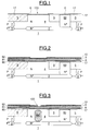
- the reference 1 designates a silicon substrate, for example of the P type, on the surface of which a buried layer 2 of extrinsic collector 2, doped N + , is produced in a conventional and known manner, by an implantation of arsenic .
- a thick epitaxy is carried out, known per se, so as to produce a layer 4 of silicon N-type monocrystalline having a thickness typically of the order 1 micron.
- a side isolation region 5 either by an oxidation process localized (or LOCOS), either of the “shallow trench” type ("Shallow Trench "). Represented in FIG. 1, for the sake of simplification, a side isolation region 5 of the shallow trench type.
- Boron implantations are then carried out so as to make beneath the lateral isolation region 5 of the boxes 7 doped P allowing isolation from transistors adjacent to the bipolar transistor described here.
- CMOS transistors complementary metal-oxide-semiconductor
- BiCMOS technology Bipolar-CMOS
- a layer 17 of amorphous silicon having a thickness of the order of 500 ⁇ .
- a window 170 called "base window”.
- both parts of the etched silicon layer 17 protrude slightly above of the intrinsic collector 4.
- the engraving window 170 can be more wider than the intrinsic collector 4.
- the second layer 81 formed of silicon-germanium is then epitaxied. It is in fact composed of a first sublayer of Si 1-x Ge x with constant x between 0.1 and 0.2, surmounted by a second sublayer also formed of an alloy of Si 1- x Ge x (with x for example decreasing to 0) and doped P with boron.
- the total thickness of the layer 81 is unimportant, typically from 20 to 100 nm.
- the second sublayer of layer 81 is then surmounted by an epitaxial layer 82 of a few tens of nanometers thick of P-doped silicon from boron.
- this epitaxy typically carried out at 700 ° C. in an ultra clean CVD deposition reactor, so a stack is obtained of monocrystalline layers on the intrinsic collector in the base window, and polycrystalline above the silicon layers amorphous 17. This stacking of layers will make it possible to form a silicon-germanium heterojunction base. It should be noted here that the heterojunction base epitaxy is an epitaxy not selective.
- the presence of the amorphous silicon layer 17 makes it possible to present a surface essentially at the start of epitaxy formed of silicon which allows a growth rate to be obtained substantially identical on the intrinsic collector and on the silicon amorphous leading to better homogeneity in base thickness.
- a first layer of silicon dioxide having a thickness of the order of 200 ⁇ is then deposited on layer 81.
- a second layer 10 of silicon nitride (Si 3 N 4 ) having a thickness of 300 ⁇ is also deposited on the first layer of silicon dioxide 9.
- the resin present on the layer of silicon nitride 10 and treatment is carried out chemical deoxidation so as to remove part of the layer of silicon dioxide 9 located in zone 100 and thus achieve the 800 transmitter window ( Figure 4).
- An example of such a chemical deoxidation treatment consists in using an acid bath based on hydrofluoric acid diluted to approximately 1% for 1 minute, which makes it possible to obtain a chemically clean surface of monocrystalline silicon, that is to say that is to say the concentration of oxygen atoms of which is less than 10 15 / cm 2 . Furthermore, such chemical deoxidation does not degrade the underlying monocrystalline silicon surface (unlike plasma etching for example) and therefore does not introduce any crystalline defects.
- a desorption treatment under high hydrogen temperature (> 550 ° C) so as to remove residual impurities adsorbed on the silicon surface during deoxidation.
- the semiconductor block is exposed with the base discovered at the level of the transmitter window 800 with a mixture gaseous silane and arsine, in a non-oxidizing atmosphere, typically under vacuum, or under hydrogen.
- the CVD deposition conditions are for example a flow rate of 10 liters of hydrogen / min, a flow rate of 0.5 liters of silane / min and a flow rate of 0.12 cm 3 of arsine / min, at 630 ° C and under a pressure of 80 Torr.
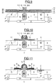
- a transmitter 11 comprising in the window 80 a lower part 110 surmounted by an upper part 111 wider than the emitter window, the distance from the edge of the emitter window and the edge of region 111 typically being about 0.2 ⁇ .
- This transmitter was therefore doped in situ and it is monocrystalline at least in the vicinity of the interface with the base in the transmitter window. It has been observed in practice that it is monocrystalline near the interface, polycrystalline above the nitride, and had a preferential orientation in the part upper epitaxial above the window.
- a block of resin is then deposited on either side of the base, as well as a resin sticker above the transmitter, then a P + implantation of the stack 8 is carried out using boron, so as to define the extrinsic base Be ( Figure 6).
- the final step consists in making the sockets of the basic S emitter and collector connections by a known technique of the "self aligned silicide” type which involves the deposition of a layer of metal (for example titanium) to form a silicide (TiSi 2 ) on the silicon zones of the extrinsic base, of the emitter and of the extrinsic collector.
- a layer of metal for example titanium
- TiSi 2 silicide
- the transistor according to the invention is therefore a heterojunction-based n-p-n vertical bipolar transistor silicon-germanium usable in a BiCMOS technology of the type VLSI. It has a monocrystalline transmitter directly in contact with the silicon of the upper encapsulation layer (82). However, due in particular to the spread of dopants and various conventional heat treatment, the emitter / base junction is located inside the layer 82.
- the transistor has a low noise reduced frequency, while maintaining good static parameters, especially the current gain. It also has resistance of transmitter reduced compared to transistors with transmitter polycrystalline.
- the distance from edge of window 800 to edge of region of the transmitter depends on the alignment of the mask photolithography used for engraving the upper region of the emitter compared to the photolithography mask used for the etching of the transmitter window itself. This makes it a little more delicate manufacturing of the transistor.
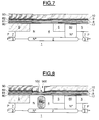
- FIGS. 7 to 11 overcomes this problem. Indeed, as illustrated on the FIG. 7, a layer of silicon nitride is deposited on a third thick layer of silicon dioxide 90 (typically having a thickness of 2000 ⁇ ). We then proceed ( Figure 8) to an engraving classic thick film plasma 90 with stop on the second layer 10 of silicon nitride, of a region 900 corresponding to the location of zone 100 of layer 10 (FIG. 3) and by Therefore at the location of the transmitter window 800. We continue the etching of the emitter window in a manner similar to that which was described in the previous embodiment. Likewise, the location of the SIC area is similar to that described above.
- the doped emitter in situ it is particularly advantageous when producing the doped emitter in situ to modulate the amount of doping gas as and when transmitter epitaxy.
- the flow rate of arsine mentioned above will for example be kept (0.12 cm 3 / min) while in the upper region of the transmitter, this flow rate will be reduced to reach for example the value of 0.6 cm 3 / min.
- a concentration of As dopant equal for example to 3 10 20 / cm 3 in the lower region of the emitter in contact with the base and a concentration of As dopant equal for example at 10 20 / cm 3 in the upper region of the transmitter.
Landscapes
- Bipolar Transistors (AREA)
Applications Claiming Priority (2)
| Application Number | Priority Date | Filing Date | Title |
|---|---|---|---|
| FR9807059 | 1998-06-05 | ||
| FR9807059A FR2779572B1 (fr) | 1998-06-05 | 1998-06-05 | Transistor bipolaire vertical a faible bruit et procede de fabrication correspondant |
Publications (1)
| Publication Number | Publication Date |
|---|---|
| EP0962966A1 true EP0962966A1 (fr) | 1999-12-08 |
Family
ID=9527036
Family Applications (1)
| Application Number | Title | Priority Date | Filing Date |
|---|---|---|---|
| EP99401337A Withdrawn EP0962966A1 (fr) | 1998-06-05 | 1999-06-03 | Transistor bipolaire vertical à faible bruit et procédé de fabrication correspondant |
Country Status (4)
| Country | Link |
|---|---|
| US (1) | US6177717B1 (enExample) |
| EP (1) | EP0962966A1 (enExample) |
| JP (1) | JP2000031155A (enExample) |
| FR (1) | FR2779572B1 (enExample) |
Cited By (1)
| Publication number | Priority date | Publication date | Assignee | Title |
|---|---|---|---|---|
| CN109887996A (zh) * | 2019-01-31 | 2019-06-14 | 上海华虹宏力半导体制造有限公司 | 自对准锗硅hbt器件的制造方法 |
Families Citing this family (28)
| Publication number | Priority date | Publication date | Assignee | Title |
|---|---|---|---|---|
| FR2801420B1 (fr) | 1999-11-23 | 2002-04-12 | St Microelectronics Sa | Transistor bipolaire vertical a faible bruit basse frequence et gain en courant eleve, et procede de fabrication correspondant |
| FR2804247B1 (fr) | 2000-01-21 | 2002-04-12 | St Microelectronics Sa | Procede de realisation d'un transistor bipolaire a emetteur et base extrinseque auto-alignes |
| FR2822292B1 (fr) * | 2001-03-14 | 2003-07-18 | St Microelectronics Sa | Procede de fabrication d'un transistor bipolaire de type double polysilicium a base a heterojonction et transistor correspondant |
| SE0103036D0 (sv) * | 2001-05-04 | 2001-09-13 | Ericsson Telefon Ab L M | Semiconductor process and integrated circuit |
| US6534802B1 (en) * | 2001-05-07 | 2003-03-18 | Newport Fab, Llc | Method for reducing base to collector capacitance and related structure |
| US6444535B1 (en) * | 2001-05-09 | 2002-09-03 | Newport Fab, Llc | Method to reduce emitter to base capacitance and related structure |
| US20020197807A1 (en) * | 2001-06-20 | 2002-12-26 | International Business Machines Corporation | Non-self-aligned SiGe heterojunction bipolar transistor |
| US6794237B2 (en) * | 2001-12-27 | 2004-09-21 | Texas Instruments Incorporated | Lateral heterojunction bipolar transistor |
| US6586297B1 (en) * | 2002-06-01 | 2003-07-01 | Newport Fab, Llc | Method for integrating a metastable base into a high-performance HBT and related structure |
| JP2004111852A (ja) * | 2002-09-20 | 2004-04-08 | Fujitsu Ltd | 半導体装置及びその製造方法 |
| CN100358110C (zh) * | 2002-12-20 | 2007-12-26 | 皇家飞利浦电子股份有限公司 | 半导体器件的制造方法 |
| DE10317098A1 (de) | 2003-04-14 | 2004-07-22 | Infineon Technologies Ag | Verfahren zur Herstellung eines Bipolartransistors |
| KR100498503B1 (ko) * | 2003-06-19 | 2005-07-01 | 삼성전자주식회사 | 바이폴라 접합 트랜지스터 및 그 제조 방법 |
| TWI250640B (en) * | 2003-06-19 | 2006-03-01 | Samsung Electronics Co Ltd | Bipolar junction transistors and methods of manufacturing the same |
| JP4711827B2 (ja) * | 2003-07-11 | 2011-06-29 | パナソニック株式会社 | ヘテロバイポーラトランジスタおよびその製造方法 |
| US6967167B2 (en) * | 2003-09-30 | 2005-11-22 | International Business Machines Corporation | Silicon dioxide removing method |
| US6979884B2 (en) * | 2003-12-04 | 2005-12-27 | International Business Machines Corporation | Bipolar transistor having self-aligned silicide and a self-aligned emitter contact border |
| FR2868203B1 (fr) * | 2004-03-29 | 2006-06-09 | St Microelectronics Sa | Procede de fabrication d'un transistor bipolaire a base extrinseque monocristalline |
| DE102004053394B4 (de) * | 2004-11-05 | 2010-08-19 | Atmel Automotive Gmbh | Halbleiteranordnung und Verfahren zur Herstellung einer Halbleiteranordnung |
| DE102004053393B4 (de) * | 2004-11-05 | 2007-01-11 | Atmel Germany Gmbh | Verfahren zur Herstellung einer vertikal integrierten Kaskodenstruktur und vertikal integrierte Kaskodenstruktur |
| US7682940B2 (en) * | 2004-12-01 | 2010-03-23 | Applied Materials, Inc. | Use of Cl2 and/or HCl during silicon epitaxial film formation |
| DE102005021450B4 (de) * | 2005-05-10 | 2009-04-23 | Atmel Germany Gmbh | Integrierter Schaltkreis und Verfahren zur Herstellung eines integrierten Schaltkreises und dessen Verwendung |
| US7342293B2 (en) * | 2005-12-05 | 2008-03-11 | International Business Machines Corporation | Bipolar junction transistors (BJTS) with second shallow trench isolation (STI) regions, and methods for forming same |
| TWI379347B (en) * | 2006-07-31 | 2012-12-11 | Applied Materials Inc | Methods of forming carbon-containing silicon epitaxial layers |
| KR101369355B1 (ko) | 2006-07-31 | 2014-03-04 | 어플라이드 머티어리얼스, 인코포레이티드 | 에피택셜 층 형성 동안에 형태를 제어하는 방법 |
| US7521772B2 (en) * | 2006-11-08 | 2009-04-21 | International Business Machines Corporation | Monocrystalline extrinsic base and emitter heterojunction bipolar transistor and related methods |
| US7723823B2 (en) * | 2008-07-24 | 2010-05-25 | Freescale Semiconductor, Inc. | Buried asymmetric junction ESD protection device |
| US11569357B2 (en) * | 2021-05-13 | 2023-01-31 | Nxp Usa, Inc. | Semiconductor device and method of making a semiconductor device |
Citations (6)
| Publication number | Priority date | Publication date | Assignee | Title |
|---|---|---|---|---|
| US5266504A (en) * | 1992-03-26 | 1993-11-30 | International Business Machines Corporation | Low temperature emitter process for high performance bipolar devices |
| US5296391A (en) * | 1982-03-24 | 1994-03-22 | Nec Corporation | Method of manufacturing a bipolar transistor having thin base region |
| US5432104A (en) * | 1993-10-07 | 1995-07-11 | Nec Corporation | Method for fabricating a vertical bipolar transistor with reduced parasitic capacitance between base and collector regions |
| DE19650493A1 (de) * | 1995-12-20 | 1997-06-26 | Korea Electronics Telecomm | Superselbstausgerichteter Bipolartransistor und Verfahren zu dessen Herstellung |
| EP0962967A1 (fr) * | 1998-06-05 | 1999-12-08 | STMicroelectronics S.A. | Procédé de dopage sélectif du collecteur intrinsèque d'un transistor bipolaire vertical à base épitaxiée |
| EP0962985A1 (fr) * | 1998-06-05 | 1999-12-08 | STMicroelectronics S.A. | Transistor bipolaire vertical comportant une base extrinsèque de rugosité réduite, et procédé de fabrication |
Family Cites Families (7)
| Publication number | Priority date | Publication date | Assignee | Title |
|---|---|---|---|---|
| JPH02150034A (ja) * | 1988-11-30 | 1990-06-08 | Fujitsu Ltd | 半導体装置およびその製造方法 |
| JP2705344B2 (ja) * | 1990-04-13 | 1998-01-28 | 日本電気株式会社 | 半導体装置及びその製造方法 |
| JP3033155B2 (ja) * | 1990-08-22 | 2000-04-17 | 日本電気株式会社 | 半導体装置の製造方法 |
| JP3172031B2 (ja) * | 1994-03-15 | 2001-06-04 | 株式会社東芝 | 半導体装置の製造方法 |
| JP2679639B2 (ja) * | 1994-09-12 | 1997-11-19 | 日本電気株式会社 | 半導体装置及びその製造方法 |
| US5834800A (en) * | 1995-04-10 | 1998-11-10 | Lucent Technologies Inc. | Heterojunction bipolar transistor having mono crystalline SiGe intrinsic base and polycrystalline SiGe and Si extrinsic base regions |
| EP0818829A1 (en) * | 1996-07-12 | 1998-01-14 | Hitachi, Ltd. | Bipolar transistor and method of fabricating it |
-
1998
- 1998-06-05 FR FR9807059A patent/FR2779572B1/fr not_active Expired - Fee Related
-
1999
- 1999-06-01 US US09/323,418 patent/US6177717B1/en not_active Expired - Lifetime
- 1999-06-03 EP EP99401337A patent/EP0962966A1/fr not_active Withdrawn
- 1999-06-03 JP JP11156049A patent/JP2000031155A/ja active Pending
Patent Citations (6)
| Publication number | Priority date | Publication date | Assignee | Title |
|---|---|---|---|---|
| US5296391A (en) * | 1982-03-24 | 1994-03-22 | Nec Corporation | Method of manufacturing a bipolar transistor having thin base region |
| US5266504A (en) * | 1992-03-26 | 1993-11-30 | International Business Machines Corporation | Low temperature emitter process for high performance bipolar devices |
| US5432104A (en) * | 1993-10-07 | 1995-07-11 | Nec Corporation | Method for fabricating a vertical bipolar transistor with reduced parasitic capacitance between base and collector regions |
| DE19650493A1 (de) * | 1995-12-20 | 1997-06-26 | Korea Electronics Telecomm | Superselbstausgerichteter Bipolartransistor und Verfahren zu dessen Herstellung |
| EP0962967A1 (fr) * | 1998-06-05 | 1999-12-08 | STMicroelectronics S.A. | Procédé de dopage sélectif du collecteur intrinsèque d'un transistor bipolaire vertical à base épitaxiée |
| EP0962985A1 (fr) * | 1998-06-05 | 1999-12-08 | STMicroelectronics S.A. | Transistor bipolaire vertical comportant une base extrinsèque de rugosité réduite, et procédé de fabrication |
Non-Patent Citations (1)
| Title |
|---|
| BURGHARTZ J N ET AL: "AN ULTRA-LOW THERMAL-BUDGET SIGE-BASE BIPOLAR TECHNOLOGY", DIGEST OF TECHNICAL PAPERS OF THE SYMPOSIUM ON VLSI TECHNOLOGY KYOTO, MAY 17 - 19, 1993, SYMPOSIUM ON VLSI TECHNOLOGY, NEW YORK, IEEE, US, PAGE(S) 59-60, 17 May 1993 (1993-05-17) * |
Cited By (2)
| Publication number | Priority date | Publication date | Assignee | Title |
|---|---|---|---|---|
| CN109887996A (zh) * | 2019-01-31 | 2019-06-14 | 上海华虹宏力半导体制造有限公司 | 自对准锗硅hbt器件的制造方法 |
| CN109887996B (zh) * | 2019-01-31 | 2022-03-08 | 上海华虹宏力半导体制造有限公司 | 自对准锗硅hbt器件的制造方法 |
Also Published As
| Publication number | Publication date |
|---|---|
| FR2779572A1 (fr) | 1999-12-10 |
| FR2779572B1 (fr) | 2003-10-17 |
| JP2000031155A (ja) | 2000-01-28 |
| US6177717B1 (en) | 2001-01-23 |
Similar Documents
| Publication | Publication Date | Title |
|---|---|---|
| EP0962966A1 (fr) | Transistor bipolaire vertical à faible bruit et procédé de fabrication correspondant | |
| EP0962967B1 (fr) | Procédé de dopage sélectif du collecteur intrinsèque d'un transistor bipolaire vertical à base épitaxiée | |
| FR2779573A1 (fr) | Transistor bipolaire vertical comportant une base extrinseque de rugosite reduite, et procede de fabrication | |
| JP3603747B2 (ja) | SiGe膜の形成方法とヘテロ接合トランジスタの製造方法、及びヘテロ接合バイポーラトランジスタ | |
| FR2804247A1 (fr) | Procede de realisation d'un transistor bipolaire a emetteur et base extrinseque auto-alignes | |
| EP1087424B1 (fr) | Procédé de fabrication d'un transistor bipolaire vertical auto-aligné | |
| JPH07183310A (ja) | 半導体装置及びその製造方法 | |
| US7183627B2 (en) | Independent control of polycrystalline silicon-germanium in an HBT and related structure | |
| EP1139407A1 (fr) | Procédé de fabrication d'un transistor bipolaire de type double-polysilicium auto-aligné à base à hétérojonction et transistor correspondant | |
| WO1999054939A1 (fr) | TRANSISTOR BIPOLAIRE VERTICAL, EN PARTICULIER A BASE A HETEROJONCTION SiGe, ET PROCEDE DE FABRICATION | |
| US7538004B2 (en) | Method of fabrication for SiGe heterojunction bipolar transistor (HBT) | |
| EP1104014A1 (fr) | Transistor vertical à faible bruit basse fréquence et gain en courant élevé, et procédé de fabrication correspondant | |
| EP1241704A1 (fr) | Procédé de fabrication d'un transistor bipolaire de type double polysilicum à base à hétérojonction et transistor correspondant | |
| EP1096557A1 (fr) | Procédé de définition de deux zones autoalignées à la surface supérieure d'un substrat | |
| JPH04162431A (ja) | 半導体装置の製造方法 | |
| EP1475830A2 (fr) | Procédé de fabrication d'un transistor bipolaire | |
| FR2803091A1 (fr) | Procede de dopage de la base extrinseque d'un transistor bipolaire | |
| JP2002525873A (ja) | バイポーラトランジスタ及びその製造方法 | |
| FR2868206A1 (fr) | Transistor bipolaire a base extrinseque monocristalline isolee du collecteur | |
| JPH1098010A (ja) | 化合物半導体低接触抵抗電極の形成方法 |
Legal Events
| Date | Code | Title | Description |
|---|---|---|---|
| PUAI | Public reference made under article 153(3) epc to a published international application that has entered the european phase |
Free format text: ORIGINAL CODE: 0009012 |
|
| AK | Designated contracting states |
Kind code of ref document: A1 Designated state(s): DE FR GB IT |
|
| AX | Request for extension of the european patent |
Free format text: AL;LT;LV;MK;RO;SI |
|
| 17P | Request for examination filed |
Effective date: 19991223 |
|
| AKX | Designation fees paid |
Free format text: DE FR GB IT |
|
| RAP1 | Party data changed (applicant data changed or rights of an application transferred) |
Owner name: FRANCE TELECOM Owner name: COMMISSARIAT A L'ENERGIE ATOMIQUE Owner name: STMICROELECTRONICS S.A. |
|
| STAA | Information on the status of an ep patent application or granted ep patent |
Free format text: STATUS: THE APPLICATION IS DEEMED TO BE WITHDRAWN |
|
| 18D | Application deemed to be withdrawn |
Effective date: 20081231 |