EP0961372B1 - Module laser à haute-fréquence et son procédé de fabrication - Google Patents
Module laser à haute-fréquence et son procédé de fabrication Download PDFInfo
- Publication number
- EP0961372B1 EP0961372B1 EP99109118A EP99109118A EP0961372B1 EP 0961372 B1 EP0961372 B1 EP 0961372B1 EP 99109118 A EP99109118 A EP 99109118A EP 99109118 A EP99109118 A EP 99109118A EP 0961372 B1 EP0961372 B1 EP 0961372B1
- Authority
- EP
- European Patent Office
- Prior art keywords
- laser
- electrical
- substrate
- laser module
- conductive path
- Prior art date
- Legal status (The legal status is an assumption and is not a legal conclusion. Google has not performed a legal analysis and makes no representation as to the accuracy of the status listed.)
- Expired - Lifetime
Links
Images


Classifications
-
- H—ELECTRICITY
- H01—ELECTRIC ELEMENTS
- H01S—DEVICES USING THE PROCESS OF LIGHT AMPLIFICATION BY STIMULATED EMISSION OF RADIATION [LASER] TO AMPLIFY OR GENERATE LIGHT; DEVICES USING STIMULATED EMISSION OF ELECTROMAGNETIC RADIATION IN WAVE RANGES OTHER THAN OPTICAL
- H01S5/00—Semiconductor lasers
- H01S5/02—Structural details or components not essential to laser action
- H01S5/022—Mountings; Housings
- H01S5/0225—Out-coupling of light
- H01S5/02253—Out-coupling of light using lenses
-
- H—ELECTRICITY
- H01—ELECTRIC ELEMENTS
- H01L—SEMICONDUCTOR DEVICES NOT COVERED BY CLASS H10
- H01L24/00—Arrangements for connecting or disconnecting semiconductor or solid-state bodies; Methods or apparatus related thereto
- H01L24/01—Means for bonding being attached to, or being formed on, the surface to be connected, e.g. chip-to-package, die-attach, "first-level" interconnects; Manufacturing methods related thereto
- H01L24/42—Wire connectors; Manufacturing methods related thereto
- H01L24/47—Structure, shape, material or disposition of the wire connectors after the connecting process
- H01L24/48—Structure, shape, material or disposition of the wire connectors after the connecting process of an individual wire connector
-
- H—ELECTRICITY
- H01—ELECTRIC ELEMENTS
- H01L—SEMICONDUCTOR DEVICES NOT COVERED BY CLASS H10
- H01L24/00—Arrangements for connecting or disconnecting semiconductor or solid-state bodies; Methods or apparatus related thereto
- H01L24/01—Means for bonding being attached to, or being formed on, the surface to be connected, e.g. chip-to-package, die-attach, "first-level" interconnects; Manufacturing methods related thereto
- H01L24/42—Wire connectors; Manufacturing methods related thereto
- H01L24/47—Structure, shape, material or disposition of the wire connectors after the connecting process
- H01L24/49—Structure, shape, material or disposition of the wire connectors after the connecting process of a plurality of wire connectors
-
- H—ELECTRICITY
- H01—ELECTRIC ELEMENTS
- H01L—SEMICONDUCTOR DEVICES NOT COVERED BY CLASS H10
- H01L2224/00—Indexing scheme for arrangements for connecting or disconnecting semiconductor or solid-state bodies and methods related thereto as covered by H01L24/00
- H01L2224/01—Means for bonding being attached to, or being formed on, the surface to be connected, e.g. chip-to-package, die-attach, "first-level" interconnects; Manufacturing methods related thereto
- H01L2224/42—Wire connectors; Manufacturing methods related thereto
- H01L2224/47—Structure, shape, material or disposition of the wire connectors after the connecting process
- H01L2224/48—Structure, shape, material or disposition of the wire connectors after the connecting process of an individual wire connector
- H01L2224/4805—Shape
- H01L2224/4809—Loop shape
- H01L2224/48091—Arched
-
- H—ELECTRICITY
- H01—ELECTRIC ELEMENTS
- H01L—SEMICONDUCTOR DEVICES NOT COVERED BY CLASS H10
- H01L2224/00—Indexing scheme for arrangements for connecting or disconnecting semiconductor or solid-state bodies and methods related thereto as covered by H01L24/00
- H01L2224/01—Means for bonding being attached to, or being formed on, the surface to be connected, e.g. chip-to-package, die-attach, "first-level" interconnects; Manufacturing methods related thereto
- H01L2224/42—Wire connectors; Manufacturing methods related thereto
- H01L2224/47—Structure, shape, material or disposition of the wire connectors after the connecting process
- H01L2224/48—Structure, shape, material or disposition of the wire connectors after the connecting process of an individual wire connector
- H01L2224/484—Connecting portions
- H01L2224/48463—Connecting portions the connecting portion on the bonding area of the semiconductor or solid-state body being a ball bond
- H01L2224/48465—Connecting portions the connecting portion on the bonding area of the semiconductor or solid-state body being a ball bond the other connecting portion not on the bonding area being a wedge bond, i.e. ball-to-wedge, regular stitch
-
- H—ELECTRICITY
- H01—ELECTRIC ELEMENTS
- H01L—SEMICONDUCTOR DEVICES NOT COVERED BY CLASS H10
- H01L2224/00—Indexing scheme for arrangements for connecting or disconnecting semiconductor or solid-state bodies and methods related thereto as covered by H01L24/00
- H01L2224/01—Means for bonding being attached to, or being formed on, the surface to be connected, e.g. chip-to-package, die-attach, "first-level" interconnects; Manufacturing methods related thereto
- H01L2224/42—Wire connectors; Manufacturing methods related thereto
- H01L2224/47—Structure, shape, material or disposition of the wire connectors after the connecting process
- H01L2224/49—Structure, shape, material or disposition of the wire connectors after the connecting process of a plurality of wire connectors
- H01L2224/491—Disposition
- H01L2224/4912—Layout
- H01L2224/49175—Parallel arrangements
-
- H—ELECTRICITY
- H01—ELECTRIC ELEMENTS
- H01L—SEMICONDUCTOR DEVICES NOT COVERED BY CLASS H10
- H01L2224/00—Indexing scheme for arrangements for connecting or disconnecting semiconductor or solid-state bodies and methods related thereto as covered by H01L24/00
- H01L2224/01—Means for bonding being attached to, or being formed on, the surface to be connected, e.g. chip-to-package, die-attach, "first-level" interconnects; Manufacturing methods related thereto
- H01L2224/42—Wire connectors; Manufacturing methods related thereto
- H01L2224/47—Structure, shape, material or disposition of the wire connectors after the connecting process
- H01L2224/49—Structure, shape, material or disposition of the wire connectors after the connecting process of a plurality of wire connectors
- H01L2224/494—Connecting portions
- H01L2224/4941—Connecting portions the connecting portions being stacked
- H01L2224/49429—Wedge and ball bonds
-
- H—ELECTRICITY
- H01—ELECTRIC ELEMENTS
- H01L—SEMICONDUCTOR DEVICES NOT COVERED BY CLASS H10
- H01L2924/00—Indexing scheme for arrangements or methods for connecting or disconnecting semiconductor or solid-state bodies as covered by H01L24/00
- H01L2924/0001—Technical content checked by a classifier
- H01L2924/00014—Technical content checked by a classifier the subject-matter covered by the group, the symbol of which is combined with the symbol of this group, being disclosed without further technical details
-
- H—ELECTRICITY
- H01—ELECTRIC ELEMENTS
- H01L—SEMICONDUCTOR DEVICES NOT COVERED BY CLASS H10
- H01L2924/00—Indexing scheme for arrangements or methods for connecting or disconnecting semiconductor or solid-state bodies as covered by H01L24/00
- H01L2924/10—Details of semiconductor or other solid state devices to be connected
- H01L2924/102—Material of the semiconductor or solid state bodies
- H01L2924/1025—Semiconducting materials
- H01L2924/10251—Elemental semiconductors, i.e. Group IV
- H01L2924/10253—Silicon [Si]
-
- H—ELECTRICITY
- H01—ELECTRIC ELEMENTS
- H01L—SEMICONDUCTOR DEVICES NOT COVERED BY CLASS H10
- H01L2924/00—Indexing scheme for arrangements or methods for connecting or disconnecting semiconductor or solid-state bodies as covered by H01L24/00
- H01L2924/19—Details of hybrid assemblies other than the semiconductor or other solid state devices to be connected
- H01L2924/191—Disposition
- H01L2924/19101—Disposition of discrete passive components
- H01L2924/19107—Disposition of discrete passive components off-chip wires
-
- H—ELECTRICITY
- H01—ELECTRIC ELEMENTS
- H01L—SEMICONDUCTOR DEVICES NOT COVERED BY CLASS H10
- H01L2924/00—Indexing scheme for arrangements or methods for connecting or disconnecting semiconductor or solid-state bodies as covered by H01L24/00
- H01L2924/30—Technical effects
- H01L2924/301—Electrical effects
- H01L2924/30107—Inductance
-
- H—ELECTRICITY
- H01—ELECTRIC ELEMENTS
- H01L—SEMICONDUCTOR DEVICES NOT COVERED BY CLASS H10
- H01L2924/00—Indexing scheme for arrangements or methods for connecting or disconnecting semiconductor or solid-state bodies as covered by H01L24/00
- H01L2924/30—Technical effects
- H01L2924/301—Electrical effects
- H01L2924/3011—Impedance
- H01L2924/30111—Impedance matching
-
- H—ELECTRICITY
- H01—ELECTRIC ELEMENTS
- H01S—DEVICES USING THE PROCESS OF LIGHT AMPLIFICATION BY STIMULATED EMISSION OF RADIATION [LASER] TO AMPLIFY OR GENERATE LIGHT; DEVICES USING STIMULATED EMISSION OF ELECTROMAGNETIC RADIATION IN WAVE RANGES OTHER THAN OPTICAL
- H01S5/00—Semiconductor lasers
- H01S5/02—Structural details or components not essential to laser action
- H01S5/022—Mountings; Housings
- H01S5/02208—Mountings; Housings characterised by the shape of the housings
- H01S5/02212—Can-type, e.g. TO-CAN housings with emission along or parallel to symmetry axis
-
- H—ELECTRICITY
- H01—ELECTRIC ELEMENTS
- H01S—DEVICES USING THE PROCESS OF LIGHT AMPLIFICATION BY STIMULATED EMISSION OF RADIATION [LASER] TO AMPLIFY OR GENERATE LIGHT; DEVICES USING STIMULATED EMISSION OF ELECTROMAGNETIC RADIATION IN WAVE RANGES OTHER THAN OPTICAL
- H01S5/00—Semiconductor lasers
- H01S5/02—Structural details or components not essential to laser action
- H01S5/022—Mountings; Housings
- H01S5/0225—Out-coupling of light
- H01S5/02255—Out-coupling of light using beam deflecting elements
-
- H—ELECTRICITY
- H01—ELECTRIC ELEMENTS
- H01S—DEVICES USING THE PROCESS OF LIGHT AMPLIFICATION BY STIMULATED EMISSION OF RADIATION [LASER] TO AMPLIFY OR GENERATE LIGHT; DEVICES USING STIMULATED EMISSION OF ELECTROMAGNETIC RADIATION IN WAVE RANGES OTHER THAN OPTICAL
- H01S5/00—Semiconductor lasers
- H01S5/02—Structural details or components not essential to laser action
- H01S5/022—Mountings; Housings
- H01S5/023—Mount members, e.g. sub-mount members
- H01S5/02325—Mechanically integrated components on mount members or optical micro-benches
-
- H—ELECTRICITY
- H01—ELECTRIC ELEMENTS
- H01S—DEVICES USING THE PROCESS OF LIGHT AMPLIFICATION BY STIMULATED EMISSION OF RADIATION [LASER] TO AMPLIFY OR GENERATE LIGHT; DEVICES USING STIMULATED EMISSION OF ELECTROMAGNETIC RADIATION IN WAVE RANGES OTHER THAN OPTICAL
- H01S5/00—Semiconductor lasers
- H01S5/04—Processes or apparatus for excitation, e.g. pumping, e.g. by electron beams
- H01S5/042—Electrical excitation ; Circuits therefor
-
- H—ELECTRICITY
- H01—ELECTRIC ELEMENTS
- H01S—DEVICES USING THE PROCESS OF LIGHT AMPLIFICATION BY STIMULATED EMISSION OF RADIATION [LASER] TO AMPLIFY OR GENERATE LIGHT; DEVICES USING STIMULATED EMISSION OF ELECTROMAGNETIC RADIATION IN WAVE RANGES OTHER THAN OPTICAL
- H01S5/00—Semiconductor lasers
- H01S5/06—Arrangements for controlling the laser output parameters, e.g. by operating on the active medium
- H01S5/062—Arrangements for controlling the laser output parameters, e.g. by operating on the active medium by varying the potential of the electrodes
- H01S5/06226—Modulation at ultra-high frequencies
-
- H—ELECTRICITY
- H01—ELECTRIC ELEMENTS
- H01S—DEVICES USING THE PROCESS OF LIGHT AMPLIFICATION BY STIMULATED EMISSION OF RADIATION [LASER] TO AMPLIFY OR GENERATE LIGHT; DEVICES USING STIMULATED EMISSION OF ELECTROMAGNETIC RADIATION IN WAVE RANGES OTHER THAN OPTICAL
- H01S5/00—Semiconductor lasers
- H01S5/06—Arrangements for controlling the laser output parameters, e.g. by operating on the active medium
- H01S5/068—Stabilisation of laser output parameters
- H01S5/0683—Stabilisation of laser output parameters by monitoring the optical output parameters
Definitions
- the invention relates to high-frequency laser modules according to the Preambles of claims 1 and 3, an optoelectronic Component, which is accommodated in a housing Has high-frequency laser module and a method for Manufacture on a variety of high frequency laser modules a semiconductor wafer according to the preamble of the claim 10th
- Such optoelectronic components come in particular in data transmission and communications technology by far Scope of use. To get as much information as possible The components are able to be transferred per unit of time usually operated in the high frequency range. The the maximum achievable data rate of the component is not determined only by the semiconductor laser used, but depends on a variety of other electrical, optical and structural measures of the entire optoelectronic component including the housing used.
- the invention is based in part on the object of creating a high-frequency laser module with an RF matching resistor R A , which can be produced together with a plurality of further high-frequency laser modules on a common substrate, with the associated semiconductor lasers being tested or aged together leave without overheating of the RF matching resistors.
- Another part of the object on which the invention is based is to provide an optoelectronic component with a housing which accommodates the high-frequency laser module according to the invention and which is designed specifically for high-frequency applications.
- the invention aims to provide a particularly efficient and inexpensive method for producing such high-frequency laser modules on a semiconductor wafer.
- the semiconductor laser can be on a secondary line common semiconductor wafer manufactured RF laser modules together with a high test or pre-aging current apply, the RF matching resistors remain de-energized and therefore unused.
- the light generated by the semiconductor laser can in itself known an electroabsorption modulator (EAM) run through and be HF-modulated by this.
- EAM electroabsorption modulator
- the intended ground contact pad of the EAM are over a on the Carrier, comprising an RF matching resistor RA RF routing connected. Since the EAM in the reverse direction is operated, i.e. essentially a small capacity represents, for the adaptation one connected in parallel to the EAM Matching resistance used.
- Through the common arrangement of semiconductor laser and EAM on the same carrier a particularly compact overall structure that is favorable for HF applications achieved, which is also easy to manufacture Way to be realized. Because the RF matching resistor within an RF routing path running on the carrier trained, he is in the immediate vicinity Proximity to the EAM, which has a favorable influence on the RF behavior of the EAM becomes.
- the invention is characterized essentially in that a provided on the carrier electrical cal contact extension bypassing the RF matching resistor R A to the RF terminal of the semiconductor laser. This in turn makes it possible to apply a test or pre-aging current to the semiconductor lasers of a plurality of RF laser modules in the pane, without current flowing through the RF matching resistor R A.
- An optical one provided in the beam path of the HF laser module Isolator can improve the RF properties of the laser module by returning reflected laser light to the laser largely prevented and in this way any annoying feedback effects significantly reduced.
- a large number of RF laser modules are produced on a common semiconductor wafer, in particular a silicon wafer.
- This has the advantage, among other things, that simple manufacturing and assembly processes are possible due to the good handling of the semiconductor wafer.
- the conductor pattern according to the invention provided on the semiconductor wafer makes it possible for a function and service life test of the RF laser modules, which is already known and is referred to as "burn-in", to continue to be carried out in the wafer assembly.
- burn-in the laser chip is subjected to a relatively high current for a predetermined period of time, which can be 48 hours or more, the stability of essential functional parameters being checked and a characterization of the laser chip being determined.
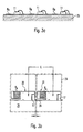
- the known laser module shown in FIG Light transmitter on a laser chip 1, which is preferably on a carrier 2 made of silicon is arranged.
- the carrier 2, which is also referred to as silicon submount, also carries two deflection prisms 3, 4 on either side of the laser chip 1 are arranged and have mirror surfaces that under an angle of 45 ° to the active surface of the laser chip 1 are oriented.
- On one deflection prism 3 a coupling lens 5 applied and arranged so that the im Laser chip 1 generated and deflected by the deflection prism 3 Laser radiation the coupling lens 5 essentially in the direction passes through its optical axis.
- the monitor chip 6 also without deflecting prism 4 directly on the support (Silicon submount) 2 attached.
- a monitor chip 6 is on the second deflection prism 4 arranged and attached that part of this from the laser chip 1 generated optical radiation is received.
- the Monitor chip 6 can be used to measure or regulate the laser power be used.
- Fig. 1b shows the laser module shown in Fig. 1a in perspective View.
- the coupling lens 5 is omitted in this figure.
- the one above Contact 7 of the laser chip 1 is via a bonding wire 8 with a contact pad attached to the edge of the carrier 2 9 connected, while the one not visible in Fig. 1b below Contact of the laser chip 1 making electrical contact stands on a conductor strip 10, which to the opposite Edge of the carrier 2 is guided and there one Has contact surface.
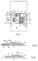
- 2a and 2b is an embodiment of an inventive HF laser module shown for high data rates.
- a semiconductor carrier 12 which preferably consists of silicon
- a laser chip 11 is arranged above a semiconductor carrier 12, which preferably consists of silicon.
- the carrier 12 stands on a housing base plate 13 which is at ground potential and is connected in series via two Bond lines 14 and 15 with the overhead (Mostly p-) contact 16 of the laser chip 11 in connection stands.
- Fig. 2b makes it clear that both the first 14 and the second 15 bond line each consisting of two (or more) individual ones Bond wires 14a, 14b and 15a, 15b be constructed can, the on a carrier 12 arranged on the ground contact pad 17 are bonded together.
- the RF data signal is fed into the area of the carrier 12 via a suitable high-frequency line.
- a microstrip line 18 is used as the data feed line, which essentially consists of a metal strip 19 which conducts the data signal, which runs above a ground conductor 20 and is guided in an insulated manner from the latter.
- the ground conductor 20 forms the underside of the microstrip line 18 and is electrically conductively connected to a ground surface on the housing base plate 13, to which the bonding wires 14a, 14b are also attached.
- the metal strip 19 is connected via two or, in a manner not shown, more HF bonding wires 21a, 21b, to one end of an HF guiding path 22 provided on the carrier 12, which at the other end is electrically connected to a contact of the laser chip 11 underneath is.
- an adaptation resistor R A is integrated into the HF routing section 22, which serves to achieve the best possible adaptation of the low-resistance laser chip 11 to the characteristic impedance of the microstrip line 18, and in the present example has a value of 22 ⁇ .
- a coaxial line or a coplanar line with RF conductor and ground strips arranged side by side can also be used as the RF feed line.
- the matching resistor R A can preferably be selected depending on the type of RF feed line used and its dimensions.
- a bias current is supplied to the laser chip 11 via the feed line 23 (Bias current) supplied.
- the HF connection at the bottom of the laser chip 11 is also connected to a branch line 24 running on the carrier 12, which enables the adaptation resistance R A to be bypassed and is of essential importance for the manufacturing process of the high-frequency laser module to be explained below.
- a silicon wafer 25 as shown in FIG. 3b, using a known technique, first a conductor pattern applied, which consists of periodically repeating conductor track structures is constructed. Two neighboring structures are shown in Fig. 3a. Give the dotted lines 26 the contours of the later carriers 12 (silicon submounts) again. It is essential that with neighboring Structures an electrical connection between the ground contact pad 17 of the one structure and the branch line 24 of the other structure.
- the laser chips 11 by soldering or others usual procedures on the designated areas L the individual conductor track structures mounted.
- the assembly process is highly automated and can therefore be opened very rational way.
- deflection prisms around the in a manner not shown Laser chips 11 grouped around and on the silicon wafer 25 attached, for example, by another soldering process can be accomplished.
- the arrangement of the deflection prisms can be selected according to the representations in FIGS. 1 and 2 become.
- the laser chips 11 mounted on the silicon wafer 25 are subjected to a common functional test or pre-aging ("burn-in").
- This test must be carried out under high current conditions in order to ensure that the individual laser chips 11 are protected for the service life within a reasonable time.
- the "burn-in" current according to the structure of the conductor pattern according to the invention is led past the matching resistors R A via the branch lines 24, so that they remain without current and no heating, let alone overheating of these resistors, can occur. This fact enables a functional test of the individual laser chips 11 with an RF matching resistor R A in the pane assembly.
- the pane can be used in the usual way separated along the dividing lines 26 into the individual submounts become.
- the submounts can then be processed individually and with, for example, a lens coupling optics 1 and 2 are provided.
- a lens coupling optics 1 and 2 are provided.
- optical components e.g. an optical isolator
- FIG. 4 shows a laser chip applied to a carrier 112 111, the semiconductor laser 113 and an integrated EAM 114 contains.
- An RF data signal is transmitted via a Microstrip line 118 and bond wires 121a, 121b into one RF connector pad 115 arranged on the carrier 112 is guided.
- the RF connection pad is connected to further bond wires 123a, 123b 115 with an RF input of the EAM 114 in electrical connection.
- the laser chip 111 lies on a ground contact pad 117, that a common ground contact for the semiconductor laser 113 and the EAM 114. Furthermore, 112 is on the carrier a bond pad 116 is provided which is connected via bond lines 124a, 124b with an overhead input terminal of the semiconductor laser 113 is connected.
- the semiconductor laser 113 is a the bond pad 116 electrically contacting lead 119 supplied with a direct current, i.e. operated in continuous wave mode.
- the RF connection pad 115 is connected to the ground contact pad 117 via an RF matching resistor R A. This is formed in an HF guiding path 122 running on the carrier 112 between the HF connection pad 115 and the ground contact pad 117 and typically has a value of approximately 50 ohms.
- the RF matching resistor R A is connected in parallel to the EAM 114 operated in the reverse direction. Due to its formation on the carrier 112 in the immediate vicinity of the EAM 114, the high-frequency properties of the module are advantageously influenced.
- ground contact pad 117 is by means of a contact extension 125 led to an edge of the carrier 112.
- the contact foothold 125 forms the carrier 112 before the separation (Submounts) an electrical connection to an approach 116a bond pad 116 of an adjacent conductor track structure and thus enables "burn-in" in the pane assembly.
- FIG. 5a shows a section through the carrier 112 with a laser chip 111 along the line I-I.
- the corresponding view in a section along the line II is shown in Fig. 5b.
- FIGS. 2a to 5b show a first example of an optoelectronic component which is operated with an RF laser module 29 according to the invention as shown in FIGS. 2a to 5b (ie either with or without an integrated EAM) and in which there are also others Measures have been taken to achieve the highest possible data rate.
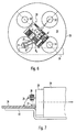
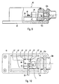
- 6 shows a top view of the internal structure of a coaxial housing 28 with a laser module 29.
- the RF signal (data signal) is fed into the interior of the housing via an insulated, for example glassed-in pin 31 and there electrically via short bonding wires or tapes 32 with the RF matching resistor R A or when using one in FIGS. 4 and 5a, 5b Laser chips 111 shown with integrated EAM 114 connected to the RF connection pad 115.
- the laser module 29 is supplied with bias current via a further feed-through pin 33. Pins 34 and 35 represent further bushings and serve to make electrical contact with monitor chip 6 '.
- the laser module 29 can be positioned in the coaxial housing 28 such that the optical axis of a coupling lens 5 'coincides with the housing center axis. Any eccentric optical axis can also be set.
- On the back of the base plate 30 of the housing 28 extends a circuit board 36, the position of which in its section covered by the housing 28 is indicated by a broken line.
- FIG. 7 shows the optoelectronic component from FIG. 6 in Side view.
- the board 36 and the coaxial housing 28 are attached to a metal ash 44, which at the same time as Ground line serves.
- the HF supply takes place via the the bottom plate 30 protruding end 37 of the pin 31.
- Da the board 36 up to the rear wall 30 of the housing 28 and also the end 37 of the HF pin 31 immediately rests on the board 36 and there with an HF conductor track is soldered or welded (see Fig. 8), can no bond wires and it becomes an overall extremely short-range electrical HF connection created.
- the housing 28 can also in a manner not shown Have ground pin that with a ground side of the board 36th is soldered. In this case, the metal ash 44 can be omitted.
- the ferrite coil 38 consists of one with at least two turns wrapped ferrite bead over a case back protruding end 39 of the bias current pin 33 is pushed.
- the bias current pin 33 can also be as short as possible connected to an RF choke on the board become. Even better RF properties are achieved if possible, the RF choke inside the TO housing 28 is arranged close to the laser chip. In this way you can Modules achieved with a bandwidth of at least 5 GHz become.
- usual optical fiber connection can be uncooled coaxial components for data rates of at least 3 Realize Gbit / s. For larger transmission distances is at high data rates (> 1Gbit / s) an optical isolator between Provide laser diode and fiber.
- Fig. 8 shows the structure shown in Fig. 7 in plan view with the corresponding connecting conductor tracks 40, 41 for the RF signal or the bias current and the other conductor tracks 42, 43 for contacting the monitor chip 6 '.
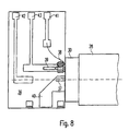
- Fig. 9 shows a second embodiment of an optoelectronic Component according to the invention.
- a cooling element 47 for example, a Peltier element.
- the HF reader module 48 is shown in Figs. 2a to 5b (i.e. with or without integrated EAM) and differs from the laser module 29 shown in FIG. 7 essentially only in that it is in the beam path behind the coupling lens 5 ' another 90 ° deflection prism is equipped and thus Laser light directed parallel to the plane of the carrier (submounts) emits.
- optical isolator 49 To avoid in the beam direction behind the HF laser module 48 of the effects of reflected light on the laser an optical isolator 49 is arranged.
- the optical isolator 49 has a good heat-conducting connection on the Cooling element 47 attached, causing an influence of the ambient temperature negligible on the optical isolator 49 can be kept low.
- a fiber coupling is provided on the outlet side of the housing, which essentially consists of a housing-side flange piece 52a and a flange piece 52b fixing the fiber 51 with integrated lens 50.
- Fig. 10 shows the component shown in Fig. 9 in plan view.
- a longitudinal side wall 53 In the area of a longitudinal side wall 53 there are a number simple electrical feedthroughs 57 for the supply and Measuring lines of the elements accommodated in the housing (For example, Peltier element, monitor chip, etc.) is provided.
- a HF bushing 56 Is located on the opposite side wall 54 an HF bushing 56, which is in the form of a through the wall Microstrip conductor 55 or in not shown Way of a coaxial line in the form of a glazed pin is executed.
- connection between the RF feedthrough 56 and the RF laser module 48 is replaced by a microstrip or Coplanar line manufactured, the respective ground lines by welding, soldering or using conductive adhesive and the signal conductor tracks are connected by means of bond wires or ribbons become.
- Both exemplary embodiments have in common that the described, the RF laser module 29; 48, the housing 28; 46 with electrical feedthroughs and optical equipment Measures a simple, inexpensive and provided an optical component suitable for high data rates becomes.
Landscapes
- Engineering & Computer Science (AREA)
- Computer Hardware Design (AREA)
- Microelectronics & Electronic Packaging (AREA)
- Power Engineering (AREA)
- Physics & Mathematics (AREA)
- Condensed Matter Physics & Semiconductors (AREA)
- General Physics & Mathematics (AREA)
- Electromagnetism (AREA)
- Optics & Photonics (AREA)
- Semiconductor Lasers (AREA)
- Optical Couplings Of Light Guides (AREA)
Claims (12)
- Module laser à haute-fréquence qui comporte un support (12), un laser (11) à semi-conducteur monté sur le support (12) et une section (22) électrique conductrice HF prévue sur le support (12) à la première extrémité de laquelle peut être appliqué un signal extérieur d'attaque HF et qui est relié à sa deuxième extrémité électriquement à une borne HF du laser (11) à semi-conducteur, la section (22) conductrice HF comprenant une résistance RA d'adaptation HF montée en série avec le laser (11) à semi-conducteur,
caractérisé en ce que
une section (24) électrique conductrice secondaire prévue sur le support (12) mène en contournant la résistance RA d'adaptation HF à la borne HF du laser (11) à semi-conducteur. - Module laser à haute-fréquence suivant la revendication 1, caractérisé en ce que la résistance RA d'adaptation HF est comprise entre 10 et 50 Ω, notamment entre 20 et 25 Ω.
- Module laser à haute-fréquence, qui comporte un support (112) une puce (111) disposée sur le support (112) et ayant un laser (113) à semi-conducteur et un modulateur (114) d'électroabsorption, une plage (115) de connexion HF prévue sur le support (112) et, en outre, une plage (117) de contact électrique de masse prévue sur le support (112) et en contact électrique avec le contact électrique de masse du modulateur (114) d'électroabsorption, et il est prévu sur le support (112) une section (122) conductrice HF reliant électriquement la plage (115) de connexion HF à la plage (117) de contact de masse et comprenant une résistance RA d'adaptation HF montée en parallèle avec le modulateur (114) d'électroabsorption,
caractérisé en ce qu'une dérivation (125) électrique de contact prévue sur le support (112) va en contournant la résistance RA d'adaptation HF à la borne HF du laser (113) à semi-conducteur. - Module laser à haute-fréquence suivant l'une des revendications précédentes, caractérisé en ce que le module laser (29, 48) comprend une optique (5') de couplage à lentille pour émettre de manière définie la lumière laser produite par le laser (11) à semi-conducteur.
- Composant opto-électronique qui comprend un module laser (29, 48) HF suivant l'une des revendications précédentes ainsi qu'un boítier (28, 46) recevant le module (29, 48) HF et ayant une traversée électrique pour le signal d'attaque HF et une fenêtre de sortie de la lumière disposée de manière appropriée.
- Composant opto-électronique suivant la revendication 5, caractérisé en ce que la traversée électrique HF a lieu au moyen d'une broche (31) qui passe à travers la paroi (30) du boítier, qui est isolée électriquement et dont l'extrémité (37) se trouvant à l'extérieur du boítier (28) est reliée électriquement, en étant notamment soudée, directement à une piste (40) conductrice HF disposée sur une platine (36).
- Composant opto-électronique suivant la revendication 5, caractérisé en ce que tant la traversée (56) électrique HF que la liaison électrique HF du côté intérieur du boítier et allant au module laser (48) est réalisée sous la forme d'une ligne coaxiale ou d'une ligne (18, 55) à ruban microscopique ou d'une ligne coplanaire.
- Composant opto-électronique suivant l'une des revendications 5 à 7, caractérisé en ce qu'il est prévu à l'intérieur ou à l'extérieur du boítier (28, 46) une inductance (38) par laquelle il est envoyé un courant de polarisation au laser (11) à semi-conducteur.
- Composant opto-électronique suivant l'une des revendications 5 à 8, caractérisé par un isolateur (49) optique monté dans le trajet du rayonnement du module laser (29, 48) HF.
- Procédé de fabrication d'une pluralité de modules laser HF sur une seule tranche semi-conductrice, caractériséa) en ce que l'on dépose sur la tranche (25) semi-conductrice un modèle de piste conductrice qui est constitué d'une structure de piste conductrice se répétant périodiquement,chaque structure individuelle de piste conductrice comprenant au moins une section (22) conductrice HF ayant une résistance RA d'adaptation HF, une section (24) conductrice secondaire contournant la résistance RA d'adaptation HF ainsi qu'une zone (17) de contact de masse isolée électriquement par rapport à la section (22) conductrice HF et par rapport à la section (24) conductrice secondaire, etdans une structure voisine de piste conductrice, la section (24) conductrice secondaire de l'une des structures est reliée électriquement à la zone (17) de contact de masse de l'autre structure ;b) en ce que, sur chaque structure, on dépose un laser (11) à semi-conducteur et on le relie électriquement à la section (22) conductrice HF et à la zone (17) de contact de masse ;c) en ce que, par l'application d'un courant de charge passant par les sections (24) conductrices secondaires, les lasers (11) à semi-conducteurs et les zones (17) de contact de masse, on effectue un essai fonctionnel commun et/ou un pré-vieillissement de plusieurs lasers (11) à semi-conducteur sur la tranche (25) semi-conductrice, etd) en ce que l'on sépare la tranche (25) semi-conductrice en modules laser (29, 48) HF individuels conformément au modèle de piste conductrice.
- Procédé suivant la revendication 10, caractérisé en ce que, avant le stade d), on dépose pour chaque laser (11) à semi-conducteur une optique (5') de couplage à lentille sur la tranche semi-conductrice.
- Procédé suivant la revendication 11, caractérisé en ce que, avant le stade d), on effectue un ajustage de l'optique (5') de couplage à lentille.
Applications Claiming Priority (2)
| Application Number | Priority Date | Filing Date | Title |
|---|---|---|---|
| DE19823479 | 1998-05-26 | ||
| DE19823479 | 1998-05-26 |
Publications (2)
| Publication Number | Publication Date |
|---|---|
| EP0961372A1 EP0961372A1 (fr) | 1999-12-01 |
| EP0961372B1 true EP0961372B1 (fr) | 2002-07-10 |
Family
ID=7868958
Family Applications (1)
| Application Number | Title | Priority Date | Filing Date |
|---|---|---|---|
| EP99109118A Expired - Lifetime EP0961372B1 (fr) | 1998-05-26 | 1999-05-07 | Module laser à haute-fréquence et son procédé de fabrication |
Country Status (4)
| Country | Link |
|---|---|
| US (1) | US6567439B1 (fr) |
| EP (1) | EP0961372B1 (fr) |
| JP (1) | JP2000012948A (fr) |
| DE (1) | DE59901985D1 (fr) |
Families Citing this family (21)
| Publication number | Priority date | Publication date | Assignee | Title |
|---|---|---|---|---|
| US6731585B2 (en) | 2000-03-03 | 2004-05-04 | Matsushita Electric Industrial Co., Ltd. | Optical pick-up head with semiconductor laser |
| US6870866B2 (en) * | 2001-06-05 | 2005-03-22 | Axcel Photonics, Inc. | Powerpack laser diode assemblies |
| US7049759B2 (en) * | 2001-12-06 | 2006-05-23 | Linear Technology Corporation | Circuitry and methods for improving the performance of a light emitting element |
| US7343535B2 (en) * | 2002-02-06 | 2008-03-11 | Avago Technologies General Ip Dte Ltd | Embedded testing capability for integrated serializer/deserializers |
| US7254149B2 (en) * | 2002-03-19 | 2007-08-07 | Finisar Corporation | Submount, pedestal, and bond wire assembly for a transistor outline package with reduced bond wire inductance |
| EP1389812A1 (fr) * | 2002-08-13 | 2004-02-18 | Agilent Technologies Inc | Configuration de montage pour les éléments électro-optique à haute frequence |
| US6881613B2 (en) * | 2002-10-08 | 2005-04-19 | Agere Systems Inc | Electronic component package |
| US7361936B2 (en) * | 2003-08-15 | 2008-04-22 | Finisar Corporation | Optical transmission and/or receiving device |
| US7520679B2 (en) * | 2003-09-19 | 2009-04-21 | Avago Technologies Fiber Ip (Singapore) Pte. Ltd. | Optical device package with turning mirror and alignment post |
| US6953990B2 (en) * | 2003-09-19 | 2005-10-11 | Agilent Technologies, Inc. | Wafer-level packaging of optoelectronic devices |
| US6982437B2 (en) * | 2003-09-19 | 2006-01-03 | Agilent Technologies, Inc. | Surface emitting laser package having integrated optical element and alignment post |
| US20050063648A1 (en) * | 2003-09-19 | 2005-03-24 | Wilson Robert Edward | Alignment post for optical subassemblies made with cylindrical rods, tubes, spheres, or similar features |
| US20050063431A1 (en) * | 2003-09-19 | 2005-03-24 | Gallup Kendra J. | Integrated optics and electronics |
| US20050213995A1 (en) * | 2004-03-26 | 2005-09-29 | Myunghee Lee | Low power and low jitter optical receiver for fiber optic communication link |
| US7295590B2 (en) * | 2004-11-15 | 2007-11-13 | Intel Corporation | Method for measuring VCSEL reverse bias leakage in an optical module |
| US9881875B2 (en) * | 2013-07-31 | 2018-01-30 | Universal Scientific Industrial (Shanghai) Co., Ltd. | Electronic module and method of making the same |
| US9379819B1 (en) * | 2014-01-03 | 2016-06-28 | Google Inc. | Systems and methods for reducing temperature in an optical signal source co-packaged with a driver |
| DE102017201285B4 (de) * | 2016-12-09 | 2021-01-28 | Fraunhofer-Gesellschaft zur Förderung der angewandten Forschung e. V. | Laseranordnung und Verfahren zum Herstellen einer Laseranordnung |
| CN111418120B (zh) * | 2017-12-04 | 2022-10-21 | 三菱电机株式会社 | 电场吸收型调制器、光半导体装置及光模块 |
| JP7350646B2 (ja) * | 2019-12-17 | 2023-09-26 | CIG Photonics Japan株式会社 | 光モジュール |
| CN114792928A (zh) * | 2021-01-25 | 2022-07-26 | 华为技术有限公司 | 激光器载体及其制作方法 |
Family Cites Families (12)
| Publication number | Priority date | Publication date | Assignee | Title |
|---|---|---|---|---|
| US4761788A (en) * | 1985-10-28 | 1988-08-02 | American Telephone And Telegraph Company | Stripline mount for semiconductor lasers |
| JPH0714102B2 (ja) * | 1988-01-28 | 1995-02-15 | 三菱電機株式会社 | 光結合装置 |
| JPH0719932B2 (ja) * | 1989-04-12 | 1995-03-06 | 三菱電機株式会社 | レーザダイオードモジュール |
| GB9100815D0 (en) * | 1991-01-15 | 1991-02-27 | British Telecomm | Coplanar waveguide ribbon |
| JPH04373155A (ja) * | 1991-06-24 | 1992-12-25 | Nippon Telegr & Teleph Corp <Ntt> | 半導体用ヒートシンク |
| JPH05110201A (ja) * | 1991-10-18 | 1993-04-30 | Nec Corp | 半導体レーザ装置 |
| JP2906868B2 (ja) * | 1992-10-14 | 1999-06-21 | 三菱電機株式会社 | レーザダイオードモジュール |
| EP0664585B1 (fr) | 1993-12-22 | 1998-03-04 | Siemens Aktiengesellschaft | Module de transmission et de réception pour système de communication bidirectionnel |
| EP0660467B1 (fr) | 1993-12-22 | 1997-03-19 | Siemens Aktiengesellschaft | Elément optoélectronique et sa méthode de fabrication |
| JP3553222B2 (ja) * | 1995-09-20 | 2004-08-11 | 三菱電機株式会社 | 光変調器モジュール |
| JPH09252164A (ja) * | 1996-03-15 | 1997-09-22 | Mitsubishi Electric Corp | レーザダイオードモジュール |
| JPH1051069A (ja) * | 1996-07-29 | 1998-02-20 | Mitsubishi Electric Corp | 光半導体装置 |
-
1999
- 1999-05-07 EP EP99109118A patent/EP0961372B1/fr not_active Expired - Lifetime
- 1999-05-07 DE DE59901985T patent/DE59901985D1/de not_active Expired - Fee Related
- 1999-05-26 JP JP11146912A patent/JP2000012948A/ja active Pending
- 1999-05-26 US US09/320,046 patent/US6567439B1/en not_active Expired - Lifetime
Also Published As
| Publication number | Publication date |
|---|---|
| US6567439B1 (en) | 2003-05-20 |
| DE59901985D1 (de) | 2002-08-14 |
| EP0961372A1 (fr) | 1999-12-01 |
| JP2000012948A (ja) | 2000-01-14 |
Similar Documents
| Publication | Publication Date | Title |
|---|---|---|
| EP0961372B1 (fr) | Module laser à haute-fréquence et son procédé de fabrication | |
| DE69434104T2 (de) | Optoelektronische Hybridintegrationsplattform und optisches Sub-Modul | |
| EP1174745B1 (fr) | Module optoélectronique montable en surface | |
| DE3822312C2 (fr) | ||
| DE19614506B4 (de) | Aufbau und Verfahren zur Auswertung von Signalzuständen in einem Sondenmeßnetzwerk | |
| DE3902579C2 (de) | Optoelektronisches Bauteil | |
| DE10152533A1 (de) | Hochfrequenz-Schaltungsplatineneinheit, Hochfrequenz-Modul, bei dem die Einheit verwendet ist, elektronische Vorrichtung, bei der das Modul verwendet ist, und Verfahren zur Herstellung der Hochfrequenz-Schaltungsplatineneinheit | |
| DE10143173A1 (de) | Wafersonde | |
| DE10050077A1 (de) | Anschlußstruktur sowie diese Anschlußstruktur enthaltende Anschlußanordnung | |
| DE10020713A1 (de) | Anschlußstruktur | |
| DE112006003458T5 (de) | Modularer Transistor-Outline-Can mit internen Bauteilen | |
| EP0111263B1 (fr) | Appareil de transmission ou réception contenant une diode dans une monture | |
| DE60313777T2 (de) | Optisches halbleiterbauelement | |
| DE102005056263B4 (de) | Elektronische Anordnung mit äußeren Impedanzabgleichskomponentenverbindungen mit nichtkompensierten Anschlussleitungen und ihr Herstellungsverfahren | |
| DE112021007591T5 (de) | Halbleiterlaser-Lichtquellenvorrichtung | |
| EP1101136B1 (fr) | Unite d'emission et de reception optoelectronique | |
| EP1168022A2 (fr) | Module opto-électronique avec substat à connexions traversantes | |
| WO1998052255A1 (fr) | Module de laser a semiconducteur haute frequence | |
| DE10128578A1 (de) | Optische Vorrichtung und ihr Herstellungsverfahren | |
| DE102021104885A1 (de) | Sockel und Gehäuse mit integriertem Kühler für elektronische Bauelemente | |
| DE10354986A1 (de) | Hochfrequenzantenne | |
| DE19824247A1 (de) | Laserdiode und insbesondere eine verbesserte Struktur einer Laserdiode mit Heteroübergang, die für Radarsysteme geeignet ist | |
| DE10132324A1 (de) | Optisches Modul | |
| DE112021006940T5 (de) | Halbleitervorrichtung | |
| DE10064577A1 (de) | Anordnung zum Betrieb eines optischen Sende-und Empfangsmodul bei hohen Datenraten bis zu 10 Gbit/s |
Legal Events
| Date | Code | Title | Description |
|---|---|---|---|
| PUAI | Public reference made under article 153(3) epc to a published international application that has entered the european phase |
Free format text: ORIGINAL CODE: 0009012 |
|
| AK | Designated contracting states |
Kind code of ref document: A1 Designated state(s): DE FR GB IT NL |
|
| AX | Request for extension of the european patent |
Free format text: AL;LT;LV;MK;RO;SI |
|
| 17P | Request for examination filed |
Effective date: 20000105 |
|
| 17Q | First examination report despatched |
Effective date: 20000602 |
|
| AKX | Designation fees paid |
Free format text: DE FR GB IT NL |
|
| RAP1 | Party data changed (applicant data changed or rights of an application transferred) |
Owner name: INFINEON TECHNOLOGIES AG |
|
| RIC1 | Information provided on ipc code assigned before grant |
Free format text: 7H 01S 5/042 A, 7H 01S 5/022 B, 7H 01L 33/00 B |
|
| GRAG | Despatch of communication of intention to grant |
Free format text: ORIGINAL CODE: EPIDOS AGRA |
|
| GRAG | Despatch of communication of intention to grant |
Free format text: ORIGINAL CODE: EPIDOS AGRA |
|
| GRAH | Despatch of communication of intention to grant a patent |
Free format text: ORIGINAL CODE: EPIDOS IGRA |
|
| GRAH | Despatch of communication of intention to grant a patent |
Free format text: ORIGINAL CODE: EPIDOS IGRA |
|
| GRAA | (expected) grant |
Free format text: ORIGINAL CODE: 0009210 |
|
| AK | Designated contracting states |
Kind code of ref document: B1 Designated state(s): DE FR GB IT NL |
|
| PG25 | Lapsed in a contracting state [announced via postgrant information from national office to epo] |
Ref country code: NL Free format text: LAPSE BECAUSE OF FAILURE TO SUBMIT A TRANSLATION OF THE DESCRIPTION OR TO PAY THE FEE WITHIN THE PRESCRIBED TIME-LIMIT Effective date: 20020710 Ref country code: IT Free format text: LAPSE BECAUSE OF FAILURE TO SUBMIT A TRANSLATION OF THE DESCRIPTION OR TO PAY THE FEE WITHIN THE PRESCRIBED TIME-LIMIT;WARNING: LAPSES OF ITALIAN PATENTS WITH EFFECTIVE DATE BEFORE 2007 MAY HAVE OCCURRED AT ANY TIME BEFORE 2007. THE CORRECT EFFECTIVE DATE MAY BE DIFFERENT FROM THE ONE RECORDED. Effective date: 20020710 |
|
| REG | Reference to a national code |
Ref country code: GB Ref legal event code: FG4D Free format text: NOT ENGLISH |
|
| REF | Corresponds to: |
Ref document number: 59901985 Country of ref document: DE Date of ref document: 20020814 |
|
| GBT | Gb: translation of ep patent filed (gb section 77(6)(a)/1977) |
Effective date: 20020912 |
|
| NLV1 | Nl: lapsed or annulled due to failure to fulfill the requirements of art. 29p and 29m of the patents act | ||
| ET | Fr: translation filed | ||
| PLBE | No opposition filed within time limit |
Free format text: ORIGINAL CODE: 0009261 |
|
| STAA | Information on the status of an ep patent application or granted ep patent |
Free format text: STATUS: NO OPPOSITION FILED WITHIN TIME LIMIT |
|
| 26N | No opposition filed |
Effective date: 20030411 |
|
| REG | Reference to a national code |
Ref country code: GB Ref legal event code: 732E |
|
| REG | Reference to a national code |
Ref country code: FR Ref legal event code: TP |
|
| PGFP | Annual fee paid to national office [announced via postgrant information from national office to epo] |
Ref country code: DE Payment date: 20080630 Year of fee payment: 10 |
|
| PGFP | Annual fee paid to national office [announced via postgrant information from national office to epo] |
Ref country code: GB Payment date: 20080529 Year of fee payment: 10 |
|
| GBPC | Gb: european patent ceased through non-payment of renewal fee |
Effective date: 20090507 |
|
| REG | Reference to a national code |
Ref country code: FR Ref legal event code: ST Effective date: 20100129 |
|
| PG25 | Lapsed in a contracting state [announced via postgrant information from national office to epo] |
Ref country code: FR Free format text: LAPSE BECAUSE OF NON-PAYMENT OF DUE FEES Effective date: 20090602 |
|
| PGFP | Annual fee paid to national office [announced via postgrant information from national office to epo] |
Ref country code: FR Payment date: 20080519 Year of fee payment: 10 |
|
| PG25 | Lapsed in a contracting state [announced via postgrant information from national office to epo] |
Ref country code: GB Free format text: LAPSE BECAUSE OF NON-PAYMENT OF DUE FEES Effective date: 20090507 |
|
| PG25 | Lapsed in a contracting state [announced via postgrant information from national office to epo] |
Ref country code: DE Free format text: LAPSE BECAUSE OF NON-PAYMENT OF DUE FEES Effective date: 20091201 |