EP0954022A1 - Verfahren zur Bereitstellung einer flachen Grabenisolation von Transistoren - Google Patents
Verfahren zur Bereitstellung einer flachen Grabenisolation von Transistoren Download PDFInfo
- Publication number
- EP0954022A1 EP0954022A1 EP99300264A EP99300264A EP0954022A1 EP 0954022 A1 EP0954022 A1 EP 0954022A1 EP 99300264 A EP99300264 A EP 99300264A EP 99300264 A EP99300264 A EP 99300264A EP 0954022 A1 EP0954022 A1 EP 0954022A1
- Authority
- EP
- European Patent Office
- Prior art keywords
- dielectric
- trenches
- nitride
- layer
- etch
- Prior art date
- Legal status (The legal status is an assumption and is not a legal conclusion. Google has not performed a legal analysis and makes no representation as to the accuracy of the status listed.)
- Granted
Links
Images


Classifications
-
- H—ELECTRICITY
- H10—SEMICONDUCTOR DEVICES; ELECTRIC SOLID-STATE DEVICES NOT OTHERWISE PROVIDED FOR
- H10D—INORGANIC ELECTRIC SEMICONDUCTOR DEVICES
- H10D84/00—Integrated devices formed in or on semiconductor substrates that comprise only semiconducting layers, e.g. on Si wafers or on GaAs-on-Si wafers
- H10D84/01—Manufacture or treatment
-
- H—ELECTRICITY
- H10—SEMICONDUCTOR DEVICES; ELECTRIC SOLID-STATE DEVICES NOT OTHERWISE PROVIDED FOR
- H10P—GENERIC PROCESSES OR APPARATUS FOR THE MANUFACTURE OR TREATMENT OF DEVICES COVERED BY CLASS H10
- H10P70/00—Cleaning of wafers, substrates or parts of devices
- H10P70/20—Cleaning during device manufacture
- H10P70/23—Cleaning during device manufacture during, before or after processing of insulating materials
- H10P70/234—Cleaning during device manufacture during, before or after processing of insulating materials the processing being the formation of vias or contact holes
-
- H—ELECTRICITY
- H10—SEMICONDUCTOR DEVICES; ELECTRIC SOLID-STATE DEVICES NOT OTHERWISE PROVIDED FOR
- H10P—GENERIC PROCESSES OR APPARATUS FOR THE MANUFACTURE OR TREATMENT OF DEVICES COVERED BY CLASS H10
- H10P14/00—Formation of materials, e.g. in the shape of layers or pillars
- H10P14/60—Formation of materials, e.g. in the shape of layers or pillars of insulating materials
- H10P14/63—Formation of materials, e.g. in the shape of layers or pillars of insulating materials characterised by the formation processes
- H10P14/6326—Deposition processes
- H10P14/6328—Deposition from the gas or vapour phase
- H10P14/6334—Deposition from the gas or vapour phase using decomposition or reaction of gaseous or vapour phase compounds, i.e. chemical vapour deposition
- H10P14/6336—Deposition from the gas or vapour phase using decomposition or reaction of gaseous or vapour phase compounds, i.e. chemical vapour deposition in the presence of a plasma [PECVD]
-
- H—ELECTRICITY
- H10—SEMICONDUCTOR DEVICES; ELECTRIC SOLID-STATE DEVICES NOT OTHERWISE PROVIDED FOR
- H10P—GENERIC PROCESSES OR APPARATUS FOR THE MANUFACTURE OR TREATMENT OF DEVICES COVERED BY CLASS H10
- H10P14/00—Formation of materials, e.g. in the shape of layers or pillars
- H10P14/60—Formation of materials, e.g. in the shape of layers or pillars of insulating materials
- H10P14/65—Formation of materials, e.g. in the shape of layers or pillars of insulating materials characterised by treatments performed before or after the formation of the materials
- H10P14/6502—Formation of materials, e.g. in the shape of layers or pillars of insulating materials characterised by treatments performed before or after the formation of the materials of treatments performed before formation of the materials
- H10P14/6506—Formation of intermediate materials
-
- H—ELECTRICITY
- H10—SEMICONDUCTOR DEVICES; ELECTRIC SOLID-STATE DEVICES NOT OTHERWISE PROVIDED FOR
- H10P—GENERIC PROCESSES OR APPARATUS FOR THE MANUFACTURE OR TREATMENT OF DEVICES COVERED BY CLASS H10
- H10P14/00—Formation of materials, e.g. in the shape of layers or pillars
- H10P14/60—Formation of materials, e.g. in the shape of layers or pillars of insulating materials
- H10P14/66—Formation of materials, e.g. in the shape of layers or pillars of insulating materials characterised by the type of materials
- H10P14/668—Formation of materials, e.g. in the shape of layers or pillars of insulating materials characterised by the type of materials the materials being characterised by the deposition precursor materials
- H10P14/6681—Formation of materials, e.g. in the shape of layers or pillars of insulating materials characterised by the type of materials the materials being characterised by the deposition precursor materials the precursor containing a compound comprising Si
- H10P14/6682—Formation of materials, e.g. in the shape of layers or pillars of insulating materials characterised by the type of materials the materials being characterised by the deposition precursor materials the precursor containing a compound comprising Si the compound being a silane, e.g. disilane, methylsilane or chlorosilane
-
- H—ELECTRICITY
- H10—SEMICONDUCTOR DEVICES; ELECTRIC SOLID-STATE DEVICES NOT OTHERWISE PROVIDED FOR
- H10P—GENERIC PROCESSES OR APPARATUS FOR THE MANUFACTURE OR TREATMENT OF DEVICES COVERED BY CLASS H10
- H10P14/00—Formation of materials, e.g. in the shape of layers or pillars
- H10P14/60—Formation of materials, e.g. in the shape of layers or pillars of insulating materials
- H10P14/69—Inorganic materials
- H10P14/692—Inorganic materials composed of oxides, glassy oxides or oxide-based glasses
- H10P14/6921—Inorganic materials composed of oxides, glassy oxides or oxide-based glasses containing silicon
- H10P14/69215—Inorganic materials composed of oxides, glassy oxides or oxide-based glasses containing silicon the material being a silicon oxide, e.g. SiO2
-
- H—ELECTRICITY
- H10—SEMICONDUCTOR DEVICES; ELECTRIC SOLID-STATE DEVICES NOT OTHERWISE PROVIDED FOR
- H10P—GENERIC PROCESSES OR APPARATUS FOR THE MANUFACTURE OR TREATMENT OF DEVICES COVERED BY CLASS H10
- H10P50/00—Etching of wafers, substrates or parts of devices
- H10P50/20—Dry etching; Plasma etching; Reactive-ion etching
- H10P50/28—Dry etching; Plasma etching; Reactive-ion etching of insulating materials
- H10P50/282—Dry etching; Plasma etching; Reactive-ion etching of insulating materials of inorganic materials
- H10P50/283—Dry etching; Plasma etching; Reactive-ion etching of insulating materials of inorganic materials by chemical means
-
- H—ELECTRICITY
- H10—SEMICONDUCTOR DEVICES; ELECTRIC SOLID-STATE DEVICES NOT OTHERWISE PROVIDED FOR
- H10P—GENERIC PROCESSES OR APPARATUS FOR THE MANUFACTURE OR TREATMENT OF DEVICES COVERED BY CLASS H10
- H10P95/00—Generic processes or apparatus for manufacture or treatments not covered by the other groups of this subclass
- H10P95/06—Planarisation of inorganic insulating materials
-
- H—ELECTRICITY
- H10—SEMICONDUCTOR DEVICES; ELECTRIC SOLID-STATE DEVICES NOT OTHERWISE PROVIDED FOR
- H10W—GENERIC PACKAGES, INTERCONNECTIONS, CONNECTORS OR OTHER CONSTRUCTIONAL DETAILS OF DEVICES COVERED BY CLASS H10
- H10W10/00—Isolation regions in semiconductor bodies between components of integrated devices
- H10W10/01—Manufacture or treatment
- H10W10/011—Manufacture or treatment of isolation regions comprising dielectric materials
- H10W10/014—Manufacture or treatment of isolation regions comprising dielectric materials using trench refilling with dielectric materials, e.g. shallow trench isolations
- H10W10/0145—Manufacture or treatment of isolation regions comprising dielectric materials using trench refilling with dielectric materials, e.g. shallow trench isolations of trenches having shapes other than rectangular or V-shape
-
- H—ELECTRICITY
- H10—SEMICONDUCTOR DEVICES; ELECTRIC SOLID-STATE DEVICES NOT OTHERWISE PROVIDED FOR
- H10W—GENERIC PACKAGES, INTERCONNECTIONS, CONNECTORS OR OTHER CONSTRUCTIONAL DETAILS OF DEVICES COVERED BY CLASS H10
- H10W10/00—Isolation regions in semiconductor bodies between components of integrated devices
- H10W10/10—Isolation regions comprising dielectric materials
- H10W10/17—Isolation regions comprising dielectric materials formed using trench refilling with dielectric materials, e.g. shallow trench isolations
Definitions
- the present invention relates to integrated circuit structures and fabrication methods, and especially to producing a planar surface after shallow trench isolation without chemical-mechanical polishing.
- Shallow Trench Isolation proceeds by etching a trench in the silicon wafer and backfilling the trench with a suitable insulator material. Since the backfill process deposits the insulator on the active areas as well as in the trench, the excess insulator material must be removed in a manner that results in a flat surface that is level with the active area surface.
- CMP chemical mechanical polishing
- the CMP process can be eliminated after shallow trench formation by a careful sequence of deposition and etch, both of which are more uniform processes than CMP.
- the trench is patterned and etched according to known methods, using a nitride mask.
- the trench is then filled using a process which simultaneously deposits and etches, such as high density plasma (HDP), producing planar surfaces over the trench and active areas and a sloped surface between the two planes.
- HDP high density plasma
- a cap nitride is then deposited over the entire surface and, together with the original nitride mask, will seal the trench from contact with the surface.
- the cap nitride is patterned, using any of various methods, including, but not limited to, photolithography, polymer spin-on and etchback, and oxide spin-on and etchback, to expose the cap nitride over the active areas only.
- the cap nitride is etched, selective to the oxide, to leave the cap only over the trenches. This exposes the oxide over the active area, which may be removed with an etch which is selective to the nitride.
- Once the oxide is removed, both the cap nitride and the original mask nitride are removed, leaving planar active area surfaces and only a small thickness of trench oxide above the surface. Processing then proceeds with known methods.
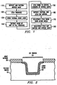
- FIG. 1 A flowchart of the disclosed method is shown in Figure 1, which will now be discussed in conjunction with Figures 2-9, which show cross-sections of the wafer at various points in the flow.
- a layer of nitride 20 is deposited and patterned (step 110) according to a known process, so that the nitride substantially covers the active areas, but exposes the trench areas.
- the trenches 25 are then etched (step 120) and a thin oxide liner 30 is typically grown (step 130), to form a structure as shown in Figure 2.
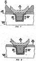
- the trench is then filled (step 140) with an oxide 40, such as silicon dioxide, which is deposited by a high density plasma (HDP) process as follows: O2 flow 150-300 sccm SiH4 flow 100-200 sccm He flow 300-500 sccm Plasma excitation power 3500-4500 watt Bias power 1500-2500 watt Wafer not clamped by electrostatic chuck
- step 150 is then performed by turning off the SiH4 flow and introducing 200-400 sccm of Ar gas for a few seconds. This should guarantee that the edges of the moat oxide will be exposed, as seen in Figure 4, since the etch of the sloped sidewalls will be faster than at the horizontal surfaces.
- a conformal nitride cap layer 50 is then deposited on the wafer, contacting the mask nitride along its top corner edges, as shown in Figure 5.
- the cap nitride 50 is then patterned and etched (step 160), using any of various methods, including, but not limited to, photolithography, polymer spin-on and etchback, or oxide spin-on and etchback, combined with an anisotropic etch, to remove the nitride over the active areas.
- This etch is chosen to be highly selective to the underlying oxide, and in this preferred embodiment is H3PO4.
- the exposed oxide is etched (step 170) to completely remove it over the active areas, as seen in Figure 8.
- This etch is chosen to be highly selective to the under-lying nitride, and in this embodiment is dilute HF.
- the oxide is removed, the remaining nitride can be removed, giving the structure seen in Figure 9.
- nitride mask e.g. silicon oxynitride.
- hydrogen-silsequioxane can be spun on instead of photoresist.
- the conditions of the spin coating and thermal processing of the HSQ are carefully controlled to position the HSQ oxide-like material only in the lowest areas of the nitride covered surface, thus making the photoresist patterning step unnecessary.
- the short etch (step 150) after oxide deposition can be a wet etch with, for example, dilute HF.
Landscapes
- Element Separation (AREA)
- Drying Of Semiconductors (AREA)
Applications Claiming Priority (2)
| Application Number | Priority Date | Filing Date | Title |
|---|---|---|---|
| US7104298P | 1998-01-13 | 1998-01-13 | |
| US71042P | 1998-01-13 |
Publications (2)
| Publication Number | Publication Date |
|---|---|
| EP0954022A1 true EP0954022A1 (de) | 1999-11-03 |
| EP0954022B1 EP0954022B1 (de) | 2010-05-12 |
Family
ID=22098896
Family Applications (1)
| Application Number | Title | Priority Date | Filing Date |
|---|---|---|---|
| EP99300264A Expired - Lifetime EP0954022B1 (de) | 1998-01-13 | 1999-01-13 | Verfahren zur Bereitstellung einer flachen Grabenisolation von Transistoren |
Country Status (6)
| Country | Link |
|---|---|
| US (1) | US6228741B1 (de) |
| EP (1) | EP0954022B1 (de) |
| JP (1) | JPH11284064A (de) |
| KR (1) | KR19990067929A (de) |
| DE (1) | DE69942356D1 (de) |
| TW (1) | TW426934B (de) |
Cited By (3)
| Publication number | Priority date | Publication date | Assignee | Title |
|---|---|---|---|---|
| WO2001033626A1 (en) * | 1999-11-02 | 2001-05-10 | Koninklijke Philips Electronics N.V. | Use of an insulating spacer to prevent threshold voltage roll-off in narrow devices |
| GB2352874B (en) * | 1999-07-01 | 2002-10-09 | Lucent Technologies Inc | An integrated circuit and a process for manufacturing the integrated circuit |
| EP1806780A3 (de) * | 2005-12-29 | 2011-06-01 | Agere Systems, Inc. | Flachen Grabenisolationsstrukturen und Verfahren zur Herstellung derselben |
Families Citing this family (9)
| Publication number | Priority date | Publication date | Assignee | Title |
|---|---|---|---|---|
| KR100419753B1 (ko) * | 1999-12-30 | 2004-02-21 | 주식회사 하이닉스반도체 | 반도체소자의 소자분리막 형성방법 |
| KR100355875B1 (ko) * | 1999-12-31 | 2002-10-12 | 아남반도체 주식회사 | 반도체 소자 분리 방법 |
| US6503813B1 (en) * | 2000-06-16 | 2003-01-07 | International Business Machines Corporation | Method and structure for forming a trench in a semiconductor substrate |
| US6531265B2 (en) * | 2000-12-14 | 2003-03-11 | International Business Machines Corporation | Method to planarize semiconductor surface |
| NZ544187A (en) | 2005-12-15 | 2008-07-31 | Ind Res Ltd | Deazapurine analogs of 1'-aza-l-nucleosides |
| US8853224B2 (en) | 2006-09-07 | 2014-10-07 | Industrial Research Limited | Acyclic amine inhibitors of nucleoside phosphorylases and hydrolases |
| HRP20150487T1 (hr) | 2010-10-15 | 2015-08-28 | Biocryst Pharmaceuticals, Inc. | Kompozicije za primjenu u lijeäśenju virusnih infekcija |
| US8859388B2 (en) | 2012-07-13 | 2014-10-14 | International Business Machines Corporation | Sealed shallow trench isolation region |
| CA3016588A1 (en) | 2016-03-06 | 2017-09-14 | Biocryst Pharmaceuticals, Inc. | Methods and compositions for treatment of zika virus infection |
Citations (5)
| Publication number | Priority date | Publication date | Assignee | Title |
|---|---|---|---|---|
| JPS6053045A (ja) * | 1983-09-02 | 1985-03-26 | Hitachi Ltd | 絶縁分離方法 |
| JPS6064445A (ja) * | 1983-09-20 | 1985-04-13 | Fujitsu Ltd | 素子分離用絶縁体層を有する半導体装置の製造方法 |
| EP0424905A2 (de) | 1989-10-25 | 1991-05-02 | Sony Corporation | Verfahren zur Herstellung einer Halbleiteranordnung |
| EP0813240A1 (de) * | 1996-06-10 | 1997-12-17 | Texas Instruments Incorporated | Verbesserungen an oder in Bezug auf Halbleiteranordnungen |
| US5721173A (en) * | 1997-02-25 | 1998-02-24 | Kabushiki Kaisha Toshiba | Method of forming a shallow trench isolation structure |
Family Cites Families (4)
| Publication number | Priority date | Publication date | Assignee | Title |
|---|---|---|---|---|
| US5786263A (en) * | 1995-04-04 | 1998-07-28 | Motorola, Inc. | Method for forming a trench isolation structure in an integrated circuit |
| US5976947A (en) * | 1997-08-18 | 1999-11-02 | Micron Technology, Inc. | Method for forming dielectric within a recess |
| US6074927A (en) * | 1998-06-01 | 2000-06-13 | Advanced Micro Devices, Inc. | Shallow trench isolation formation with trench wall spacer |
| US5976951A (en) * | 1998-06-30 | 1999-11-02 | United Microelectronics Corp. | Method for preventing oxide recess formation in a shallow trench isolation |
-
1999
- 1999-01-11 US US09/228,583 patent/US6228741B1/en not_active Expired - Lifetime
- 1999-01-13 JP JP11006782A patent/JPH11284064A/ja active Pending
- 1999-01-13 EP EP99300264A patent/EP0954022B1/de not_active Expired - Lifetime
- 1999-01-13 KR KR1019990001110A patent/KR19990067929A/ko not_active Withdrawn
- 1999-01-13 DE DE69942356T patent/DE69942356D1/de not_active Expired - Lifetime
- 1999-03-12 TW TW088100431A patent/TW426934B/zh not_active IP Right Cessation
Patent Citations (5)
| Publication number | Priority date | Publication date | Assignee | Title |
|---|---|---|---|---|
| JPS6053045A (ja) * | 1983-09-02 | 1985-03-26 | Hitachi Ltd | 絶縁分離方法 |
| JPS6064445A (ja) * | 1983-09-20 | 1985-04-13 | Fujitsu Ltd | 素子分離用絶縁体層を有する半導体装置の製造方法 |
| EP0424905A2 (de) | 1989-10-25 | 1991-05-02 | Sony Corporation | Verfahren zur Herstellung einer Halbleiteranordnung |
| EP0813240A1 (de) * | 1996-06-10 | 1997-12-17 | Texas Instruments Incorporated | Verbesserungen an oder in Bezug auf Halbleiteranordnungen |
| US5721173A (en) * | 1997-02-25 | 1998-02-24 | Kabushiki Kaisha Toshiba | Method of forming a shallow trench isolation structure |
Non-Patent Citations (3)
| Title |
|---|
| ANONYMOUS: "Selective Planarization Process and Structures", IBM TECHNICAL DISCLOSURE BULLETIN, vol. 27, no. 4B, New York, US, pages 2560 - 2563, XP002110920 * |
| PATENT ABSTRACTS OF JAPAN vol. 009, no. 181 (E - 331) 26 July 1985 (1985-07-26) * |
| PATENT ABSTRACTS OF JAPAN vol. 009, no. 197 (E - 335) 14 August 1985 (1985-08-14) * |
Cited By (5)
| Publication number | Priority date | Publication date | Assignee | Title |
|---|---|---|---|---|
| GB2352874B (en) * | 1999-07-01 | 2002-10-09 | Lucent Technologies Inc | An integrated circuit and a process for manufacturing the integrated circuit |
| WO2001033626A1 (en) * | 1999-11-02 | 2001-05-10 | Koninklijke Philips Electronics N.V. | Use of an insulating spacer to prevent threshold voltage roll-off in narrow devices |
| KR100707535B1 (ko) * | 1999-11-02 | 2007-04-12 | 코닌클리즈케 필립스 일렉트로닉스 엔.브이. | 절연 스페이서 및 얕은 트렌치 분리 영역 형성 방법과절연 리세싱으로부터 얕은 트렌치 영역을 보호하는 방법 |
| EP1806780A3 (de) * | 2005-12-29 | 2011-06-01 | Agere Systems, Inc. | Flachen Grabenisolationsstrukturen und Verfahren zur Herstellung derselben |
| US8022481B2 (en) | 2005-12-29 | 2011-09-20 | Agere Systems Inc. | Robust shallow trench isolation structures and a method for forming shallow trench isolation structures |
Also Published As
| Publication number | Publication date |
|---|---|
| US6228741B1 (en) | 2001-05-08 |
| DE69942356D1 (de) | 2010-06-24 |
| EP0954022B1 (de) | 2010-05-12 |
| KR19990067929A (ko) | 1999-08-25 |
| TW426934B (en) | 2001-03-21 |
| JPH11284064A (ja) | 1999-10-15 |
Similar Documents
| Publication | Publication Date | Title |
|---|---|---|
| KR100279016B1 (ko) | 반도체 제조시 비-컨포멀 디바이스 층을 평탄화하는 방법 | |
| US6372605B1 (en) | Additional etching to decrease polishing time for shallow-trench isolation in semiconductor processing | |
| KR100224700B1 (ko) | 반도체장치의 소자분리방법 | |
| US5262346A (en) | Nitride polish stop for forming SOI wafers | |
| KR100604816B1 (ko) | 집적 회로 소자 리세스 트랜지스터의 제조 방법 및 이에의해 제조된 집적회로 소자 리세스 트랜지스터 | |
| US6159822A (en) | Self-planarized shallow trench isolation | |
| US6228741B1 (en) | Method for trench isolation of semiconductor devices | |
| US20020004284A1 (en) | Method for forming a shallow trench isolation structure including a dummy pattern in the wider trench | |
| KR100307651B1 (ko) | 반도체장치의제조방법 | |
| US6171929B1 (en) | Shallow trench isolator via non-critical chemical mechanical polishing | |
| JPH05315441A (ja) | ポリッシュ工程を備えた半導体装置の製造方法 | |
| US6258697B1 (en) | Method of etching contacts with reduced oxide stress | |
| US5830773A (en) | Method for forming semiconductor field region dielectrics having globally planarized upper surfaces | |
| KR19980063317A (ko) | 반도체장치의 소자분리방법 | |
| US20010029083A1 (en) | Method for forming shallow trench isolation structure | |
| US6087262A (en) | Method for manufacturing shallow trench isolation structure | |
| US6403492B1 (en) | Method of manufacturing semiconductor devices with trench isolation | |
| US6060348A (en) | Method to fabricate isolation by combining locos and shallow trench isolation for ULSI technology | |
| US6559028B1 (en) | Method of topography management in semiconductor formation | |
| US7981802B2 (en) | Method for manufacturing shallow trench isolation layer of semiconductor device | |
| US6489193B1 (en) | Process for device isolation | |
| KR20000015466A (ko) | 트렌치 격리의 제조 방법 | |
| US7371665B2 (en) | Method for fabricating shallow trench isolation layer of semiconductor device | |
| JPH1167891A (ja) | 素子分離体の形成方法 | |
| US20020076653A1 (en) | Novel method to planarize semiconductor surface |
Legal Events
| Date | Code | Title | Description |
|---|---|---|---|
| PUAI | Public reference made under article 153(3) epc to a published international application that has entered the european phase |
Free format text: ORIGINAL CODE: 0009012 |
|
| AK | Designated contracting states |
Kind code of ref document: A1 Designated state(s): DE FI GB IT NL |
|
| AX | Request for extension of the european patent |
Free format text: AL;LT;LV;MK;RO;SI |
|
| 17P | Request for examination filed |
Effective date: 20000503 |
|
| AKX | Designation fees paid |
Free format text: DE FI GB IT NL |
|
| 17Q | First examination report despatched |
Effective date: 20070511 |
|
| RIN1 | Information on inventor provided before grant (corrected) |
Inventor name: WALSH, SHAWN T. Inventor name: CAMPBELL, JAMES E. Inventor name: FREDIMANN, JAMES B. Inventor name: PARRILL, DR. THOMAS M. Inventor name: JAN, DR. DER'E Inventor name: ROBBINS, JOSHUA J. Inventor name: AHLBURN, BYRON T. Inventor name: CRANCK, SUE ELLEN |
|
| GRAP | Despatch of communication of intention to grant a patent |
Free format text: ORIGINAL CODE: EPIDOSNIGR1 |
|
| GRAS | Grant fee paid |
Free format text: ORIGINAL CODE: EPIDOSNIGR3 |
|
| GRAA | (expected) grant |
Free format text: ORIGINAL CODE: 0009210 |
|
| AK | Designated contracting states |
Kind code of ref document: B1 Designated state(s): DE FI GB IT NL |
|
| REG | Reference to a national code |
Ref country code: GB Ref legal event code: FG4D |
|
| REF | Corresponds to: |
Ref document number: 69942356 Country of ref document: DE Date of ref document: 20100624 Kind code of ref document: P |
|
| REG | Reference to a national code |
Ref country code: NL Ref legal event code: T3 |
|
| PG25 | Lapsed in a contracting state [announced via postgrant information from national office to epo] |
Ref country code: FI Free format text: LAPSE BECAUSE OF FAILURE TO SUBMIT A TRANSLATION OF THE DESCRIPTION OR TO PAY THE FEE WITHIN THE PRESCRIBED TIME-LIMIT Effective date: 20100512 |
|
| PLBE | No opposition filed within time limit |
Free format text: ORIGINAL CODE: 0009261 |
|
| STAA | Information on the status of an ep patent application or granted ep patent |
Free format text: STATUS: NO OPPOSITION FILED WITHIN TIME LIMIT |
|
| PG25 | Lapsed in a contracting state [announced via postgrant information from national office to epo] |
Ref country code: IT Free format text: LAPSE BECAUSE OF FAILURE TO SUBMIT A TRANSLATION OF THE DESCRIPTION OR TO PAY THE FEE WITHIN THE PRESCRIBED TIME-LIMIT Effective date: 20100512 |
|
| 26N | No opposition filed |
Effective date: 20110215 |
|
| REG | Reference to a national code |
Ref country code: DE Ref legal event code: R097 Ref document number: 69942356 Country of ref document: DE Effective date: 20110214 |
|
| PGFP | Annual fee paid to national office [announced via postgrant information from national office to epo] |
Ref country code: GB Payment date: 20131227 Year of fee payment: 16 |
|
| PGFP | Annual fee paid to national office [announced via postgrant information from national office to epo] |
Ref country code: DE Payment date: 20140131 Year of fee payment: 16 Ref country code: NL Payment date: 20140108 Year of fee payment: 16 |
|
| REG | Reference to a national code |
Ref country code: DE Ref legal event code: R119 Ref document number: 69942356 Country of ref document: DE |
|
| REG | Reference to a national code |
Ref country code: NL Ref legal event code: V1 Effective date: 20150801 |
|
| GBPC | Gb: european patent ceased through non-payment of renewal fee |
Effective date: 20150113 |
|
| PG25 | Lapsed in a contracting state [announced via postgrant information from national office to epo] |
Ref country code: NL Free format text: LAPSE BECAUSE OF NON-PAYMENT OF DUE FEES Effective date: 20150801 |
|
| PG25 | Lapsed in a contracting state [announced via postgrant information from national office to epo] |
Ref country code: GB Free format text: LAPSE BECAUSE OF NON-PAYMENT OF DUE FEES Effective date: 20150113 Ref country code: DE Free format text: LAPSE BECAUSE OF NON-PAYMENT OF DUE FEES Effective date: 20150801 |