EP0954006A2 - Verfahren zur Herstellung einer Elektronen emittierenden Vorrichtung,einer Elektronenquelle und eines Bilderzeugungsgeräts - Google Patents
Verfahren zur Herstellung einer Elektronen emittierenden Vorrichtung,einer Elektronenquelle und eines Bilderzeugungsgeräts Download PDFInfo
- Publication number
- EP0954006A2 EP0954006A2 EP99303355A EP99303355A EP0954006A2 EP 0954006 A2 EP0954006 A2 EP 0954006A2 EP 99303355 A EP99303355 A EP 99303355A EP 99303355 A EP99303355 A EP 99303355A EP 0954006 A2 EP0954006 A2 EP 0954006A2
- Authority
- EP
- European Patent Office
- Prior art keywords
- electron
- image
- substrate
- electric field
- forming
- Prior art date
- Legal status (The legal status is an assumption and is not a legal conclusion. Google has not performed a legal analysis and makes no representation as to the accuracy of the status listed.)
- Granted
Links
Images


Classifications
-
- H—ELECTRICITY
- H01—ELECTRIC ELEMENTS
- H01J—ELECTRIC DISCHARGE TUBES OR DISCHARGE LAMPS
- H01J1/00—Details of electrodes, of magnetic control means, of screens, or of the mounting or spacing thereof, common to two or more basic types of discharge tubes or lamps
- H01J1/02—Main electrodes
- H01J1/30—Cold cathodes, e.g. field-emissive cathode
-
- H—ELECTRICITY
- H01—ELECTRIC ELEMENTS
- H01J—ELECTRIC DISCHARGE TUBES OR DISCHARGE LAMPS
- H01J9/00—Apparatus or processes specially adapted for the manufacture, installation, removal, maintenance of electric discharge tubes, discharge lamps, or parts thereof; Recovery of material from discharge tubes or lamps
- H01J9/02—Manufacture of electrodes or electrode systems
- H01J9/022—Manufacture of electrodes or electrode systems of cold cathodes
- H01J9/027—Manufacture of electrodes or electrode systems of cold cathodes of thin film cathodes
Definitions
- the present invention relates to a method for producing an electron-emitting device, a method for producing an electron source, and a method for producing an image-forming apparatus.
- Examples of the surface conduction electron-emitting devices include those disclosed in M. I. Elinson, Radio Eng. Electron Phys., 10, 1290 (1965), and so on.
- the surface conduction electron-emitting devices utilize such a phenomenon that electron emission occurs when electric current is allowed to flow in parallel to the surface in a thin film of a small area formed on a substrate.
- Examples of the electron-emitting devices reported heretofore include those using a thin film of SnO 2 by Elinson et al. cited above, those using a thin film of Au [G. Dittmer: “Thin Solid Films,” 9, 317 (1972)], those using a thin film of In 2 O 3 /SnO 2 [M. Hartwell and C. G. Fonstad: "IEEE Trans. ED Conf.,” 519, (1975)], those using a thin film of carbon [Hisashi Araki et al.: Shinku (Vacuum), Vol. 26, No. 1, p22 (1983)], and so on.
- a typical example of these electron-emitting devices is the device structure of M. Hartwell cited above, which is schematically shown in Fig. 19.
- an electrically conductive, thin film 4 is formed on a substrate 1.
- the electrically conductive, thin film 4 is, for example, a thin film of a metallic oxide formed by sputtering in an H-shaped pattern and an electron-emitting region 5 is formed therein by an energization operation called energization forming.
- the gap L between the device electrodes is set to 0.5 to 1 mm and the width W' to 0.1 mm.
- the surface conduction electron-emitting devices described above have an advantage of capability of forming an array of many devices across a large area readily, because of their simple structure and easy production.
- a variety of applications have been studied heretofore in order to take advantage of this feature. For example, they are applied to charged beam sources, image-forming apparatus (display devices), and so on.
- An example of the application to formation of an array of many surface conduction emitting devices is, as described below, an electron source comprised of a lot of rows, each row being formed by arraying the electron-emitting devices in parallel and connecting the both ends of the individual devices by wires (which will also be referred to as common wires).
- the flat panel type image-forming devices (display devices) using the liquid crystal are becoming widespread while replacing the CRTs, but they had problems including one that they needed to have a back light, because they were not self-emission type devices.
- An example of the self-emission type image-forming devices (display devices) is an image-forming apparatus, which is an image-forming device (display device) constructed in the form of a combination of an electron source having an array of many surface conduction emitting devices with a fluorescent member for emitting visible light upon reception of electrons emitted from the electron source (for example, USP No. 5,066,883).
- USP No. 3,896,016 discloses the problem of Na ions in the application of soda lime glass to the substrate of the liquid crystal display devices.
- the electrodes are placed on the both front and back surfaces of soda lime glass and an electric field is applied at the same time as heating. This operation decreases Na ions in one surface of soda lime glass, so as to suppress influence thereof to the liquid crystal.
- Japanese Laid-open Patent Application No. 9-17333 discloses a problem in the surface conduction electron-emitting device where on a glass substrate containing an alkali such as Na or the like, the device electrodes are formed with a paste containing sulfur and an organometal.
- the Japanese application discloses that the aforementioned paste is printed and baked on the substrate of alkali-containing glass such as soda lime glass or the like whereby a compound containing Na and sulfur is deposited on the surface of the device electrodes.
- this compound makes instable electrical connection between the conductive film and the device electrodes.
- Disclosed as a means for solving it is a process having steps of forming the device electrodes, thereafter cleaning them together with the substrate, and then forming the electroconductive film thereon.
- alkali-containing glass particularly, soda lime glass
- Fig. 22A and Fig. 22B are schematic diagrams to show a conventional surface conduction electron-emitting device.
- Fig. 22A is a schematic plan view of the device and
- Fig. 22B is a schematic, sectional view of Fig. 22A.
- the electroconductive film 4 on which an electron-emitting region 5 is placed is formed in contact with the surface of the substrate 1.
- Figs. 23A to 23D are schematic diagrams to show a method of producing the surface conduction electron-emitting device described above.
- the surface conduction electron-emitting device is made, for example, as follows.
- electrodes 2, 3 are formed on the substrate 1 (Fig. 23A).
- the electroconductive film is formed so as to make connection between the electrodes 2, 3 (Fig. 23B).
- the electroconductive film is formed after formation of the electrodes 2, 3 in this example, but there are also cases where the electrodes are formed after formation of the electroconductive film to the contrary.
- an energization forming step is carried out to energize the electroconductive film 4.
- the energization method is, for example, a method for energizing the electroconductive film 4 by applying such a voltage that a potential of one electrode out of the pair of electrodes described above becomes higher than a potential of the other electrode. This energization forms a small gap 11 in the conductive film (Fig. 23C).
- an energization activation step to energize the electroconductive film is carried out in such a state that the region near the aforementioned gap part is in contact with an atmosphere in which an organic substance is present.
- This step is to form a carbon film 10 on the substrate in the gap 11 and on the electroconductive film 4 near the gap (Fig. 23D).
- the activation step results in forming a second gap 12 of the carbon film narrower than the gap 11, in the gap 11 formed by the aforementioned forming.
- the voltage applied in this activation step is preferably set to a voltage higher than the voltage applied in the above forming step in order to obtain the carbon film with higher quality.
- the electron-emitting region 5 is formed through the above steps.
- the energization operation is necessary for formation of the electron-emitting region 5 in the surface conduction electron-emitting device.
- a conceivable reason is that part of the energy supplied with application of the voltage between the aforementioned pair of electrodes 2, 3 is dissipated in the substrate 1 because of the effects including superposition of conduction (direct current) in the substrate due to the movement of Na ions, energy loss due to dielectric polarization (dielectric loss), generation of internal electromotive force, and so on.
- an electron source obtained would be one with nonuniform electron emission characteristics.
- An object of the present invention is, therefore, to provide a novel method for suppressing the influence of the Na ions during the energization operation.
- the present invention is characterized by a method for producing an electron-emitting device, the method comprising:
- the Na ions can be made to move from the first principal surface side, on which the electroconductive film is formed, to the back surface side of the substrate.
- the energization operation for the electroconductive film such as the energization forming operation, the energization activation operation, or the like, carried out after the electric field application step can be carried out on a stable basis and this permits us to obtain the electron-emitting device, the electron source, and the image-forming apparatus with excellent repeatability and uniformity.
- the strength of the electric field applied in the electric field application step is preferably not more than 20 kV/cm.
- the electric field application step is preferably carried out in a state in which the substrate is heated.
- the electric field application step is carried out upon heating the substrate, the movement of Na ions is promoted, so that the time necessary for the movement of the Na ions can be decreased.
- the above heating method can be any method; for example, heating can be achieved by placing a heating means such as a heater in close contact with the second principal surface. Another means for heating is to place the substrate in a heating means such as a furnace for heating the entire substrate.
- the aforementioned electric field application step is preferably a step of applying such a voltage that a potential applied to a plurality of wires for driving the electron-emitting devices is different from a potential applied to electrodes placed on the second principal surface.
- an image-forming apparatus comprising an electron source having an array of electron-emitting devices, and an image-forming member
- the vessel is also heated during evacuation of the inside of the vessel to a depressurized state after the sealing step, it is preferable to apply the aforementioned electric field during this heating as well.
- Fig. 1A and Fig. 1B are diagrams to show the features of the present invention best, which are schematic diagrams to show an example of the electron-emitting device according to the present invention.
- Fig. 1A device electrodes 2, 3 and electroconductive film 4 are provided on the substrate 1.
- a back electrode 6 on the back surface of the substrate, as illustrated in Fig. 1B.
- Figs. 1A and 1B are the schematic diagrams to show the structure of the electron-emitting device to which the present invention can be applied, wherein Fig. 1A is a plan view of the device and Fig. 1B is a sectional view of the device.
- Fig. 1A there are provided the electrodes 2, 3, electroconductive film 4, and electron-emitting region 5 on the substrate 1 and the back electrode 6 on the back surface of the substrate 1.
- the electrodes 2 and 3 are provided for forming suitably an electrical energizing of the electroconductive film 4.
- the electrodes 2 and 3 are not necessarily required.
- the substrate 1 is a glass substrate containing sodium.
- a cheaper soda lime glass may be used for the substrate.
- the sodium is contained in several kinds of the glass material.
- boro-silicated glass substrate containing sodium may also be used for the present invention.
- a substrate produced by laminating SiO 2 on those glass by sputtering may be used. Wherein, by laminating SiO 2 , a precipitation of Na compound from the substrate can be produced.
- a material for the device electrodes 2, 3 opposed to each other can be an ordinary conductive material. It can be properly selected, for example, from metals such as Ni, Cr, Au, Mo, W, Pt, Ti, Al, Cu, Pd, and the like, alloys thereof, printed conductors composed of a metal or a metal oxide such as Pd, Ag, Au, RuO 2 , Pd-Ag, or the like and glass or the like, transparent conductive materials such as In 2 O 3 -SnO 2 or the like, semiconductor/conductor materials such as polysilicon or the like, and so on.
- metals such as Ni, Cr, Au, Mo, W, Pt, Ti, Al, Cu, Pd, and the like, alloys thereof, printed conductors composed of a metal or a metal oxide such as Pd, Ag, Au, RuO 2 , Pd-Ag, or the like and glass or the like, transparent conductive materials such as In 2 O 3 -SnO 2 or the like, semiconductor/conductor materials such as
- the gap L between the device electrodes, the length W of the device electrodes, the shape of the conductive film 4, etc. are designed, taking an application form or the like into consideration.
- the device electrode gap L can be determined preferably in the range of several thousand angstroms to several hundred micrometers and more preferably in the range of several micrometers to several ten micrometers, taking the voltage placed between the device electrodes or the like into consideration.
- the device electrode width W can be determined in the range of several micrometers to several hundred micrometers, taking the resistance of the electrodes and the electron emission characteristics into consideration.
- the device can also be constructed in such structure that the conductive film 4 and the opposed device electrodes 2, 3 are stacked in the stated order on the substrate 1.
- the thickness of the conductive film 4 is properly determined, taking the step coverage over the device electrodes 2, 3, the resistance between the device electrodes 2, 3, the forming conditions described hereinafter, and so on into consideration. Normally, the thickness of the conductive film 4 is determined preferably in the range of several angstroms to several thousand angstroms and more preferably in the range of 10 angstroms to 500 angstroms. The surface resistance Rs of the conductive film 4 is preferably in the range of 10 2 to 10 7 ⁇ / ⁇ .
- the material for making the electroconductive film 4 is properly selected from metals such as Pd, Pt, Ru, Ag, Au, Ti, In, Cu, Cr, Fe, Zn, Sn, Ta, W, Pb, and so on, oxides such as PdO, SnO 2 , In 2 O 3 , PbO, Sb 2 O 3 , and so on, borides such as HfB 2 , ZrB 2 , LaB 6 , CeB 6 , YB 4 , GdB 4 , and so on, carbides such as TiC, ZrC, HfC, TaC, SiC, WC, and so on, nitrides such as TiN, ZrN, HfN, and so on, semiconductors such as Si, Ge, and so on, carbon, and so on.
- metals such as Pd, Pt, Ru, Ag, Au, Ti, In, Cu, Cr, Fe, Zn, Sn, Ta, W, Pb, and so on
- oxides such as Pd
- the electron-emitting region 5 is comprised of a gap formed in part of the electroconductive film 4 by the energization forming and, preferably, a carbon film placed on the substrate in the aforementioned gap and on the electroconductive film near the gap by energization activation described hereinafter.
- the gap is one dependent on the thickness, quality, material and techniques of the energization forming or the like described hereinafter of the electroconductive film 4, and so on.
- the carbon film can be one containing carbon and a carbon compound.
- an organometallic solution is applied onto the substrate 1 provided with the device electrodes 2, 3 to form a thin film of an organic metal.
- the organometallic solution can be a solution of an organometallic compound containing the principal element of the metal in the material of the conductive film 4 described above.
- the organometallic film is heated and baked and then is patterned by lift-off, etching, or the like, thereby forming the conductive film 4 (Fig. 3B).
- the methods for forming the conductive film 4 do not always have to be limited thereto; for example, the conductive film 4 can also be formed by either one selected from the vacuum evaporation process, the sputtering process, the chemical vapor deposition process, the dispersion coating method, the dipping method, the spinner method, the ink jet method, and so on.
- the ink jet method is preferably used, because it can obviate the need for the patterning step described above.
- a positive voltage with respect to the back electrode 6 is applied to the device electrodes 2, 3 in order to reduce Na ions in the surface (Fig. 3C).
- An application method of the voltage can be a method for connecting the back surface of the substrate to the ground and applying the positive voltage to the front surface of the substrate or a method for connecting the surface of the substrate to the ground and applying a negative voltage to the back surface of the substrate. If the substrate is heated at this time the Na ions can be moved efficiently in a short time.
- the voltage applied is preferably determined in the range of the strength of the electric field not more than 20 kV/cm. When an electric field strength exceeds 20 kV/cm, a dielectric breakdown would likely be caused in the glass substrate.
- the waveforms of the voltage are preferably pulse waveforms.
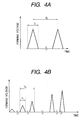
- For applying such pulses there are a method illustrated in Fig. 4A for continuously applying pulses with a pulse peak height of a constant voltage and a method illustrated in Fig. 4B for applying pulses with increasing pulse peak heights.
- the activation step is a step by which the device current If and emission current I e are changed remarkably.
- the organic substances applicable include saturated hydrocarbons represented by C n H 2n+2 such as methane, ethane, propane, and the like, unsaturated hydrocarbons represented by the composition formula of C n H 2n or the like such as ethylene, propylene, and the like, benzene, benzonitrile, toluene, methanol, ethanol, formaldehyde, acetaldehyde, acetone, methyl ethyl ketone, methylamine, ethylamine, phenol, formic acid, acetic acid, propionic acid, and so on.
- This operation causes carbon or a carbon compound to be deposited on the substrate within the gap formed in the above forming step and on the conductive film near the gap from the organic substance existing in the ambience.
- This step forms the electron-emitting region 5 (Fig. 3D).
- the judgment of the end of the activation step is properly made while measuring the device current If and the emission current I e .
- the pulse width, the pulse interval, the pulse peak heights, etc. are properly determined as occasion may demand.
- the carbon and carbon compound mean, for example, graphite (including so-called HOPG, PG, and GC; HOPG indicating nearly perfect graphite crystal structure, PG indicating slightly disordered crystal structure having the crystal grains of about 200 angstroms, and GC indicating much more disordered crystal structure having the crystal grains of about 20 angstroms) or non-crystalline carbon (indicating amorphous carbon and a mixture of amorphous carbon with fine crystals of the aforementioned graphite).
- the thickness of the carbon film is preferably in the range of not more than 500 angstroms and more preferably in the range of not more than 300 angstroms.
- the electron-emitting device obtained through these steps is preferably subjected to a stabilization step.
- This step is a step of exhausting the organic substance from the vacuum vessel.
- a vacuum evacuation apparatus for evacuating the vacuum vessel is preferably one not using oil in order to prevent oil generated from the apparatus from affecting the characteristics of the device.
- the vacuum evacuation apparatus can be selected from an absorption pump, an ion pump, and so on.
- the ambience during driving of the electron-emitting device after completion of the stabilization step is preferably that at the time of completion of the above stabilization operation, but it is not limited to this. As long as the organic substance is removed well, sufficiently stable characteristics can be maintained even with a little degradation of the degree of vacuum itself.
- measurement can be carried out under such conditions that the voltage of the anode electrode 54 is set in the range of 1 kV to 10 kV and the distance H between the anode electrode 54 and the electron-emitting device is in the range of 2 mm to 8 mm.
- Equipment necessary for measurement under a vacuum atmosphere such as a vacuum gage or the like not illustrated, is provided in the vacuum vessel 55 and is adapted to perform the measurement and evaluation under a desired vacuum atmosphere.
- the exhaust pump 56 is composed of an ordinary high vacuum system consisting of a turbo pump, a rotary pump, etc. and, further, an ultra-high vacuum system consisting of an ion pump etc.
- the whole of the vacuum process apparatus in which the electron source substrate is placed, illustrated herein, can be heated up to 200 °C by a heater not illustrated. Therefore, the steps of the aforementioned energization forming and after can also be performed using this vacuum process apparatus.
- Fig. 6 is a schematic diagram to show the relationship of the emission current I e and device current I f , measured using the vacuum process apparatus illustrated in Fig. 5, versus the device voltage V f .
- Fig. 6 is illustrated in arbitrary units, because the emission current I e is extremely smaller than the device current I f .
- the abscissa and ordinate both are linear scales.
- this device increases the emission current I e suddenly with application of the device voltage not less than a certain voltage (which will be called a threshold voltage; V th in Fig. 6) and the emission current I e is rarely detected with the device voltage not more than the threshold voltage V th .
- the device is a nonlinear device having the definite threshold voltage V th against the emission current I e .
- the emission current I e has monotonically increasing dependence on the device voltage V f , the emission current I e can be controlled by the device voltage V f .
- emission charge captured by the anode electrode 54 is dependent on the time of application of the device voltage V f . Namely, the charge amount captured by the anode electrode 54 can be controlled by the time of application of the device voltage V f .
- the electron-emitting device according to the present invention is an electron-emitting device the electron emission characteristics of which can be controlled readily according to an input signal.
- the electron-emitting device according to the present invention can be applied to equipment in various fields, including an electron source comprised of a plurality of such electron-emitting devices, an image-forming apparatus, and so on.
- Fig. 6 shows the example in which the device current I f monotonically increases against the device voltage V f (hereinafter referred to as "MI characteristics"), which is indicated by the solid line. It is noted that there are cases in which the device current I f demonstrates the voltage-controlled negative resistance characteristics (hereinafter referred to as "VCNR characteristics”) against the device voltage V f (though not illustrated). These characteristics can be controlled by controlling the aforementioned steps.
- MI characteristics the device current I f monotonically increases against the device voltage V f
- VCNR characteristics voltage-controlled negative resistance characteristics
- An example is a ladder-like configuration in which a lot of electron-emitting devices arranged in parallel are connected each at the both ends to wires, many rows of electron-emitting devices are arranged (in a row direction), and electrons from the electron-emitting devices are controlled by control electrodes (which are also referred to as grid electrodes) disposed above the aforementioned electron-emitting devices and along a direction perpendicular to the wires (i.e., in a column direction).
- control electrodes which are also referred to as grid electrodes
- Another example is a configuration in which plural electron-emitting devices are arrayed in a matrix pattern along the X-direction and along the Y-direction, first electrodes of plural electron-emitting devices arranged in each row are connected to a common X-directional wire, and second electrodes of plural electron-emitting devices arranged in each column are connected to a common Y-directional wire.
- This configuration is a so-called simple matrix configuration. First, the simple matrix configuration will be detailed below.
- the electron-emitting device has the three characteristics described previously. Namely, electrons emitted from the electron-emitting device can be controlled by the peak height and width of the pulsed voltage applied between the opposed device electrodes in the range not less than the threshold voltage. On the other hand, electrons are rarely emitted in the range not more than the threshold voltage. According to this characteristic, in the case of the configuration comprised of many electron-emitting devices, electron emission amounts can also be controlled for selected electron-emitting devices, according to the input signal, by properly applying the pulsed voltage to the individual devices.
- Fig. 7 an electron source substrate obtained by arraying a plurality of electron-emitting devices according to the present invention.
- Fig. 7 there are X-directional wires 73, Y-directional wires 72, electron-emitting devices 74, and connecting wires 75 formed on an electron source substrate 71.
- the m X-directional wires 73 are comprised of D x1 , D x2 ,..., D xm and can be constructed of a conductive metal or the like made by vacuum evaporation, printing, sputtering, or the like. The material, thickness, and width of the wires are designed properly as occasion may demand.
- the Y-directional wires 72 are n wires of D y1 , D y2 ,..., D yn and are made in a similar fashion to the X-directional wires 73.
- An interlayer insulating layer not illustrated is provided between these m X-directional wires 73 and n Y-directional wires 72, thereby electrically separating them from each other (where m, n are both positive integers).
- the interlayer insulating layer not illustrated is made of SiO 2 or the like by vacuum evaporation, printing, sputtering, or the like.
- the thickness, material, and production method of the insulating layer are properly set so that the interlayer insulating layer is formed on the entire surface or in a desired pattern on part of the substrate 71 on which the X-directional wires 73 are formed and, particularly, so that the insulating layer can withstand potential differences at intersecting portions between the X-directional wires 73 and the Y-directional wires 72.
- the X-directional wires 73 and Y-directional wires 72 are drawn out as external terminals.
- the material for the wires 72 and the wires 73, the material for the connecting wires 75, and the material for the pairs of device electrodes may share some or all of constituent elements or may be different from each other. These materials are properly selected, for example, from the aforementioned materials for the device electrodes. If the material for the device electrodes is the same as the material for the wires, the wires connected to the device electrodes can be regarded as device electrodes.
- an unrepresented scanning signal applying means for applying a scanning signal for selecting a row of surface conduction emitting devices 74 aligned in the X-direction.
- an unrepresented modulation signal generating means for modulating each column of surface conduction emitting devices 74 aligned in the Y-direction, according to the input signal.
- a driving voltage applied to each electron-emitting device is supplied as a difference voltage between the scanning signal and the modulation signal applied to the device described previously.
- FIG. 20A to 20C An example of a method for producing the electron source in the simple matrix configuration described above will be explained referring to Figs. 20A to 20C and Figs. 21A to 21C.
- Figs. 20A to 20C and Figs. 21A to 21C show an example for fabricating nine devices for simplicity of explanation.
- the wires 73 can also be formed by other forming methods of wires 73, of course, including the sputtering method etc. as described above.
- a paste containing the material for the wires 73 is printed on the substrate 1 through a screen having apertures in the pattern of the column-directional wires and the paste thus printed is heated and baked to form the wires 73.
- the interlayer insulating layer 75 is formed, at least, at the intersecting portions between the column-directional wires 73 and the row-directional wires (Fig. 20C).
- a preferred method for forming the interlayer insulating layer 75 is the screen printing method that can form the layer easily and simply over a large area.
- a preferred pattern of the interlayer insulating layer is such a comb-teeth shape as to cover the intersecting portions between the column-directional wires and the row-directional wires and permit the row-directional wires to be connected to the device electrodes 3, as illustrated in Fig. 20C.
- the interlayer insulating layer 75 can also be formed by other forming methods, of course, including the sputtering method etc. as described above.
- the interlayer insulating layer is formed by the screen printing method, a paste containing an insulating material is printed on the substrate 1 through a screen having apertures in the pattern of the interlayer insulating layer and the paste thus printed is heated and baked to form the interlayer insulating layer 75.
- the row-directional wires 72 (Y-directional wires or upper wires) are formed so as to be in contact with the other-side electrodes 3 out of the device electrodes (Fig. 21A).
- a preferred method for forming the wires 72 is the screen printing method that can form the wires easily and simply over a large area.
- Fig. 8 is a schematic diagram to show an example of a display panel of the image-forming apparatus
- Figs. 9A and 9B are schematic diagrams of fluorescent films used in the image-forming apparatus of Fig. 8.
- Fig. 10 is a block diagram to show an example of driving circuitry for carrying out the display according to TV signals of the NTSC system.
- Fig. 9A and Fig. 9B are schematic diagrams to show fluorescent films.
- the fluorescent film 84 can be made of only a fluorescent material in the monochrome case.
- the fluorescent film can be made of a black member 91, called black stripes or a black matrix or the like, and fluorescent materials 92.
- the black stripes can be made of a material containing graphite as a matrix, or can also be made of any electroconductive material with little transmission and reflection of light.
- the image-forming apparatus illustrated in Fig. 8 is produced, for example, as follows.
- the electron source substrate also serves as a rear plate.
- the support frame 82 is mounted on the portion where the frit was placed on the electron source substrate, and the face plate is further mounted so that the frit glass preliminarily deposited on the face plate is overlaid on the support frame 82.
- the envelope 88 While being heated, if necessary, similar to the aforementioned stabilization step, the envelope 88 is evacuated through an unrepresented exhaust pipe by an exhaust device not using oil, such as the ion pump, the absorption pump, or the like, down to the atmosphere containing little organic substance in the degree of vacuum of about 10 -7 Torr, and the sealing is then effected.
- a getter operation can also be performed in order to maintain the degree of vacuum after the sealing of the envelope 88. This is an operation for heating a getter placed at a predetermined position (not illustrated) inside the envelope 88 by heating using resistance heating, high-frequency heating, or the like immediately before execution of the sealing of the envelope 88 or after the sealing thereof to form an evaporated film.
- the getter is normally one containing the principal component of Ba or the like, which maintains, for example, the degree of vacuum of 1 ⁇ 10 -5 to 1 ⁇ 10 -7 Torr by adsorption of the evaporated film.
- the steps of the forming operation and after of the electron-emitting devices can be set as occasion may demand.
- the display panel 101 is connected to the external circuits via the terminals D ox1 to D oxm , the terminals D oy1 to D oyn , and high-voltage terminal Hv.
- Applied to the terminals D ox1 to D oxm are scanning signals for successively driving the electron source disposed in the display panel, i.e., the group of electron-emitting devices arranged in the matrix wiring pattern of m rows ⁇ n columns, row by row (every n devices).
- dc voltage for example, of 10 kV from the dc voltage supply V a , which is an accelerating voltage for imparting sufficient energy for excitation of the fluorescent material to the electron beams emitted from the electron-emitting devices.
- the scanning circuit 102 will be described.
- This circuit includes m switching devices (schematically indicated by S 1 to S m in the drawing) inside.
- Each switching device selects either the output voltage of the dc voltage supply V x or 0 V (the ground level) to be electrically connected to the terminal D x1 to D xm of the display panel 101.
- Each switching device S 1 to S m operates based on a control signal T scan outputted from the control circuit 103 and can be constructed, for example, of a combination of switching devices such as FETs.
- the dc voltage supply V x is set to output such a constant voltage that the driving voltage applied to the devices not scanned is not more than the electron emission threshold voltage, based on the characteristic (electron emission threshold voltage) of the electron-emitting device.
- the control circuit 103 has the function to match operations of the respective sections with each other so as to carry out the appropriate display based on the image signals supplied from the outside.
- the control circuit 103 generates control signals of T scan , T sft , and T mry to the respective sections, based on a synchronous signal T sync sent from the synchronous signal separating circuit 106.
- the shift register 104 is provided for effecting serial/parallel conversion every line of image with the DATA signal serially inputted in time series and operates based on the control signal T sft sent from the control circuit 103. (In other words, the control signal T sft can also be mentioned as a shift clock of the shift register 104.) Data of one line of image after the serial/parallel conversion (corresponding to driving data for N electron-emitting devices) is outputted as N parallel signals of I d1 to I dn from the shift register 104.
- the electron-emitting devices have the following basic characteristics as to the emission current I e .
- the devices have the definite threshold voltage V th for emission of electron, so that emission of electron occurs only when the voltage not less than V th is applied.
- the emission current also varies according to change of the voltage applied to each device. From this feature, where the pulsed voltage is applied to the device, emission of electron does not take place, for example, with application of a voltage not more than the electron emission threshold voltage, but an electron beam is outputted with application of a voltage not less than the electron emission threshold voltage.
- the intensity of the output electron beam can be controlled by changing the peak height V m of pulse.
- the total amount of charge of the output electron beam can be controlled by changing the width P w of pulse.
- a voltage modulation method, a pulse duration modulation method, and so on can be employed as a method for modulating the electron-emitting devices according to the input signal.
- the modulation signal generator 107 can be a circuit of the voltage modulation method capable of generating voltage pulses of a constant length and properly modulating peak heights of the pulses according to the input data.
- the modulation signal generator 107 can be a circuit of the pulse duration modulation method capable of generating voltage pulses with a constant peak height and properly modulating the widths of the voltage pulses according to the input data.
- the output signal DATA of the synchronous signal separating circuit 106 needs to be digitized and it is implemented by an A/D converter disposed at an output portion of the synchronous signal separating circuit 106.
- the circuit used in the modulation signal generator 107 differs slightly, depending upon whether the output signals of the line memory 105 are digital signals or analog signals. Namely, in the case of the voltage modulation method using digital signals, the modulation signal generator 107 is, for example, a D/A converter and an amplifier or the like is added thereto if necessary.
- the modulation signal generator 107 is a circuit, for example, obtained by combining a high-speed oscillator and a counter for counting the number of waves output from the oscillator with a comparator for comparing an output value from the counter with an output value from the memory.
- An amplifier can also be added for voltage-amplifying the modulation signal modified in pulse duration, output from the comparator, up to the driving voltage of the electron-emitting device, if necessary.
- electron emission occurs when the signal voltage and scanning voltage are applied to each electron-emitting device via the external terminals D ox1 to D oxm , D oy1 to D oyn outside the vessel.
- the high voltage is applied via the high-voltage terminal Hv to the metal back 85 or to a transparent electrode (not illustrated), thereby accelerating the electron beams.
- the fluorescent film 84 is bombarded with the electrons thus accelerated to bring about luminescence, thereby forming an image.
- the structure of the image-forming apparatus described herein is just an example of the image-forming apparatus according to the present invention and a variety of modifications can be made based on the technical concept of the present invention.
- the input signals were of the NTSC system, but the input signals are not limited to this system.
- they can be signals of the PAL system, the SECAM system, or the like, or signals of systems of TV signals comprised of more scanning lines than the foregoing systems (for example, high-definition TV systems including the MUSE system, and the ATV system).
- the voltage not less than the electron emission threshold is applied to a device row expected to emit electron beams, whereas the voltage not more than the electron emission threshold is applied to a device row expected not to emit electron beams.
- the common wires D x2 to D x9 between the device rows can also be formed as single wires; for example, D x2 and D x3 can be made as a single wire.
- the grid electrodes 122 are provided between the substrate 110 and the face plate 86.
- the grid electrodes 122 are given for the purpose of modulating the electron beams emitted from the surface conduction emitting devices and are provided with circular pores 121 each per device in order to let the electron beams pass the stripe-shape electrodes perpendicular to the device rows of the ladder-shape configuration.
- the shape and arrangement of the grid electrodes are not limited to those illustrated in Fig. 12.
- the pores can be a lot of pass holes in a mesh pattern and the grid electrodes can be located around or near the surface conduction emitting devices.
- the outside terminals D x1 , D x2 ,..., D xm and grid terminals G 1 , G 2 ,..., G n are electrically connected to the control circuit not illustrated.
- modulation signals for one line of image are applied simultaneously to the grid electrode array in synchronism with successive driving (scanning) of the device rows row by row. This permits the image to be displayed line by line with controlling irradiation of each electron beam onto the fluorescent material.
- the image-forming apparatus of the present invention can be used as an image-forming apparatus (a display device) for television broadcasting or an image-forming apparatus (a display device) for a video conference system, a computer, or the like and in addition, it can also be used as an image-forming apparatus or the like as an optical printer constructed using a photosensitive drum or the like.
- Figs. 1A and 1B there are the device electrodes 2, 3, the electron-emitting region 5, and the electroconductive film 4 provided on the substrate 1 and the back electrode 6 on the back surface of the substrate 1.
- a pattern expected to become the device electrodes 2, 3 and the gap between the device electrodes was formed with a photoresist and then Ti and Ni were successively deposited in the thickness of 50 angstroms and in the thickness of 1000 angstroms, respectively, in the stated order by vacuum evaporation. Then the photoresist pattern was dissolved with an organic solvent, and the Ni/Ti deposited films were lifted off, thereby forming the device electrodes 2, 3 having the device electrode gap L1 of 10 ⁇ m and the device electrode width W of 300 ⁇ m. Further, Pt was deposited in the thickness of 1000 angstroms on the back surface, thereby forming the back electrode 6 (Fig. 3A).
- a Cr film having the thickness of 1000 angstroms was deposited by vacuum evaporation and patterned, and then organic Pd was spin-coated thereon with a spinner. The heating and baking operation was carried out at 300 °C for ten minutes.
- the conductive film 4 containing the principal element of Pd thus formed had the thickness of 100 angstroms and the sheet resistance of 2 ⁇ 10 4 ⁇ / ⁇ .
- the Cr film and the conductive film 4 after baked were etched with an acid etchant to form a desired pattern.
- the device electrodes 2, 3 and the conductive film 4 were formed on the substrate 1 through the above steps (Fig. 3B).
- a positive voltage with respect to the back electrode 6 was applied to the device electrodes 2, 3 as illustrated in Fig. 3C.
- the thickness of the substrate was 2.8 mm, the voltage applied was 1 kV, and the time of application was 2 hours.
- the current density of the current flowing at this time was 7.1 ⁇ 10 -10 A/cm 2 and the charge moved in one hour was 4.8 ⁇ 10 -6 C.
- Most of carriers for electric conduction in the soda lime glass were Na ions, so that this step c caused the Na ions to move from the front surface of the substrate toward the back surface of the substrate. Therefore, the concentration of Na ions near the front surface decreased remarkably.
- the substrate was set in the measurement/evaluation device of Fig. 5 and the inside thereof was evacuated by a vacuum pump. After arrival at the vacuum degree of 2 ⁇ 10 -6 Torr, the voltage was placed between the device electrodes 2, 3 from the power supply 51 for applying the device voltage Vf to the device, thereby effecting the energization operation (forming operation).
- the voltage waveforms in the forming operation are illustrated in Fig. 24.
- T1 and T2 represent the pulse width and the pulse interval of the voltage waveforms.
- the forming operation was carried out under such conditions that T1 was 1 msec, T2 was 10 msec, and the peak heights of rectangular waves (the peak voltages during the forming) were increased by steps of 0.1 V.
- resistance-measuring pulses were placed in the voltage of 0.1 V during the intervals T2 to measure the resistance. It was assumed that the end of the forming operation was at the time when the measurement with the resistance-measuring pulse became about 1 M ⁇ or more. At that timing the application of the voltage to the device was stopped.
- the forming voltage V of the device was 5.1 V.
- the measurement was carried out under such conditions that the distance between the anode electrode and the electron-emitting device was 4 mm, the potential of the anode electrode was 1 kV, and the degree of vacuum in the vacuum device during the measurement of electron emission characteristics was 1 ⁇ 10 -6 Torr.
- the voltage was applied as a device voltage between the electrodes 2 and 3 of the present device and the device current If and emission current Ie flowing at that time were measured.
- the result obtained was the current-voltage characteristics as illustrated in Fig. 6. Since the amount of Na ions in the front surface of the substrate was decreased and became smaller than before, the steps of the forming and after became stable and the yield was improved thereby. Further, variations were decreased in the characteristics among devices. Particularly, where a plurality of electron-emitting devices were formed on a single substrate, the uniformity of electron emission characteristics was improved greatly.
- the second example will be described as an example in which the substrate is heated during the application of voltage.
- Figs. 2A and 2B there are the device electrodes 2, 3, the conductive film 4, and the electron-emitting region 5 provided on the substrate 1. Further, the back electrode 6 is provided on the back surface of the substrate 1. The substrate 1 is heated with a heater 7 for heating of substrate.
- the steps up to step b before the application of the electric field to the substrate were similar to those in Example 1. The steps of the application of the electric field and after will be described in order below.
- Fig. 18 shows the relation between electric conductivity and temperature of soda lime glass.
- the time at 60 °C can be decreased by the magnitude of about one order.
- the voltage of 1 kV was applied for ten minutes to the front surface of the substrate.
- the heating enabled more reduction of time than in Example 1. Since the electric conductivity varies with the heating of substrate as described above, the voltage and application time can be adjusted by changing the temperature for heating the substrate.
- resistance-measuring pulses were placed in the voltage of 0.1 V during the intervals T2 to measure the resistance. It was assumed that the end of the forming operation was at the time when the measurement with the resistance-measuring pulse became about 1 M ⁇ or more. At that timing the application of the voltage to the device was stopped.
- the forming voltage V of the device was 5.0 V.
- the device after the forming operation was subjected to the energization activation operation.
- the application of the voltage pulses was carried out under such conditions that the peak heights of the rectangular waves in the waveforms of Fig. 25 were 14 V, the pulse width was 100 ⁇ s, and the repetition frequency was 10 Hz, thereby forming the electron-emitting region 5.
- the measurement of the electron emission characteristics of the device produced according to the above steps was carried out using the measurement/evaluation device of Fig. 5.
- the measurement was carried out under such conditions that the distance between the anode electrode and the electron-emitting device was 4 mm, the potential of the anode electrode was 1 kV, and the degree of vacuum in the vacuum device during the measurement of electron emission characteristics was 1 ⁇ 10 -6 Torr.
- the forming operation was carried out by applying the rectangular pulses between the electrodes of the device during the formation of the electron-emitting region and the activation was carried out by applying the rectangular pulses; however, without having to be limited to the above waveforms, the waveforms applied between the electrodes of the device can also be any desired waveforms selected from rectangular waves, triangular waves, trapezoid waves, sinusoidal waves, and so on.
- the peak heights, the pulse width, the pulse interval, etc. do not always have to be limited to the aforementioned values, either, and desired values can be selected therefor in the scope of the present invention as long as the electron-emitting region is formed in good order.
- FIG. 13 A plan view of part of the electron source is illustrated in Fig. 13.
- FIG. 14 A cross-sectional view along line 14-14 in the same figure is illustrated in Fig. 14.
- the same reference symbols denote the same elements in Fig. 13, Fig. 14, Fig. 15, and Fig. 16.
- the X-directional wires (which will also be referred to as lower wires) 73 corresponding to Dxn of Fig. 7
- the Y-directional wires (which will also be referred to as upper wires) 72 corresponding to Dyn of Fig. 7, the conductive films 4, the electron-emitting regions 5, the device electrodes 2, 3, the interlayer insulating layer 131, contact holes 132 for electrical connection between the device electrodes 2 and the lower wires 73, etc. provided on the substrate 1.
- a soda lime glass plate after cleaned, to obtain a substrate 1 and Cr and Au were successively deposited in the thickness of 50 ⁇ and in the thickness of 6000 ⁇ , respectively, on the substrate 1 by vacuum evaporation. Thereafter, a photoresist was spin-coated by a spinner and baked. Thereafter, the photomask image was exposed and developed to form a resist pattern of the lower wires 73. Then the Au/Cr deposited films were wet-etched to form the lower wires 73 in the desired pattern (a" of Fig. 15).
- the interlayer insulating layer 131 of a silicon oxide film 1.0 ⁇ m thick was deposited by RF sputtering (b" of Fig. 15).
- a photoresist pattern for forming the contact holes 132 was formed on the silicon oxide film deposited in step b" and, using this as a mask, the interlayer insulating layer 131 was etched to form the contact holes 132.
- the etching was RIE (Reactive Ion Etching) using CF 4 and H 2 gases (c" of Fig. 15).
- a pattern expected to become the device electrodes 2, 3 and the gaps G between the device electrodes was formed with a photoresist and Ti and Ni were successively deposited thereon in the thickness of 50 ⁇ and in the thickness of 1000 ⁇ , respectively, by vacuum evaporation.
- the photoresist pattern was dissolved with an organic solvent and the Ni/Ti deposited films were lifted off, thereby forming the device electrodes 2, 3.
- the device electrode gap G was 10 ⁇ m and the device electrode width was 300 ⁇ m.
- Pt was deposited on the back surface of the substrate by sputtering to form the back electrode (not illustrated) (d" of Fig. 15).
- a Cr film having the thickness of 1000 angstroms was deposited by vacuum evaporation and patterned, and then organic Pd was spin-coated thereon with the spinner. The heating and baking operation was carried out at 300 °C for ten minutes.
- the conductive film 4 containing the principal element of Pd thus formed had the thickness of 100 angstroms and the sheet resistance of 5 ⁇ 10 4 ⁇ / ⁇ (f" of Fig. 16).
- the Cr film and the conductive film 4 after baked were etched with an acid etchant to form the desired pattern (g" of Fig. 16).
- the lower wires 73, the interlayer insulating layer 131, the upper wires 72, the device electrodes 2, 3, and the conductive films 4 were formed on the insulating substrate 1 by the above steps.
- the electron source substrate 71 in Fig. 8 indicates the same one as the above electron source substrate before the forming.
- the fluorescent film 84 which would be made of only the fluorescent material in the monochrome case, was formed in the stripe pattern of the fluorescent materials in the present example; specifically, the fluorescent film 84 was made by first forming the black stripes and applying the three primary color fluorescent materials to the gap portions.
- the fluorescent materials were applied by the slurry method to the glass substrate 83 with a material containing graphite as a matrix, which is commonly used as a material for the black stripes.
- the metal back 85 was provided on the inside surface side of the fluorescent film 84.
- the metal back was made by, after fabrication of the fluorescent film, carrying out a smoothing operation (normally called filming) of the inside surface of the fluorescent film and thereafter depositing Al by vacuum evaporation.
- the face plate 86 is sometimes provided with a transparent electrode (not illustrated) on the outside surface side of the fluorescent film in order to further enhance the electrical conduction property of the fluorescent film 84, but sufficient electrical conduction was achieved by only the metal back in the present example. Therefore, the transparent electrode was not provided.
- the atmosphere inside the glass vessel (envelope) completed as described above was evacuated through the exhaust pipe (not illustrated) by the vacuum pump down to a sufficient vacuum degree.
- the glass vessel was heated to 60 °C and thereafter the voltage was placed between the device electrodes 2, 3 and the back electrode 6 through the outside terminals Dx1 to Dxm and Dy1 to Dyn.
- the voltage was applied for ten minutes while keeping the back electrode 6 at 0 V and the device electrodes 2, 3 at 1 kV.
- This step can decrease the Na ions near the front surface of the substrate on which the conductive films are formed and the steps after this step, i.e., the steps including the forming, activation, driving, etc., can be performed on a stable basis.
- the voltage was placed between the device electrodes 2 and 3 through the outside terminals Dx1 to Dxm and Dy1 to Dyn, thereby effecting the energization forming operation.
- the voltage waveforms of the forming operation were the same as in Fig. 24.
- the activation operation was conducted with the same rectangular waves at the peak height of 14 V as in the forming, while measuring the device current If and emission current Ie.
- the application of the voltage was carried out in the similar fashion to that in the forming; the voltage was placed between the device electrodes 2, 3 through the outside terminals Dx1 to Dxm and Dy1 and Dyn, whereby the carbon film was deposited around each gap formed by the forming.
- a voltage which was determined in consideration with the wiring resistance, was applied from the outside in order to apply the same voltage between the device electrodes in every device.
- a better method is to carry out the activation of plural devices by successively scanning the application of the voltage with time, so as to uniform the characteristics of the respective devices.
- the scanning signal and modulation signal were applied each from the unrepresented signal generating means through the outside terminals Dx1 to Dxm, Dy1 to Dyn to each electron-emitting device, whereby each electron-emitting device emitted electrons.
- the high voltage of several kV or more was applied to the metal back 85 through the high-voltage terminal Hv to accelerate electron beams.
- the electron beams hit the fluorescent film 84 to bring about excitation and luminescence, thereby displaying an image.
- the present example is an example of the image-forming apparatus in which a lot of surface conduction electron-emitting devices are arrayed in the simple matrix configuration.
- the voltage application step of Example 3 is carried out at the same time as the sealing step.
- the atmosphere inside the glass vessel completed as described above was evacuated to a sufficient vacuum degree through the exhaust pipe (not illustrated) by the vacuum pump. After that, the voltage was applied between the device electrodes 2 and 3 through the outside terminals Dx1 to Dxm and Dy1 to Dyn, thereby effecting the forming operation.
- the voltage waveforms in the forming operation were the same as in Fig. 24.
- the activation operation was conducted with the same rectangular waves at the peak height of 14 V as in the forming, while measuring the device current If and emission current Ie.
- the application of the voltage was carried out in the similar fashion to that in the forming; the voltage was placed between the device electrodes 2, 3 through the outside terminals Dx1 to Dxm and Dy1 and Dyn, whereby the carbon film was deposited around each gap formed by the forming.
- a voltage which was determined in consideration with the wiring resistance, was applied from the outside in order to apply the same voltage between the device electrodes in every device.
- a better method is to carry out the activation of plural devices by successively scanning the application of the voltage with time, so as to uniform the characteristics of the respective devices.
- the forming and activation operation were carried out to form the electron-emitting regions 5, thereby producing the electron-emitting devices 74. Since the Na ions in the front surface of the substrate became less than in Example 3, the steps after the forming became stable and the yield was improved thereby. In addition, the variations became smaller in the characteristics among the devices and thus the uniformity was improved drastically. Further, since the sealing step and the voltage application step were carried out simultaneously, the steps were able to be decreased. In addition, since the high temperature during the sealing was able to be utilized, the voltage applied was decreased and there remained no electric field in the substrate after the application of voltage.
- the inside of the envelope was evacuated down to the vacuum degree of about 10 -6 Torr and the exhaust pipe not illustrated was heated with a gas burner to be fused, thereby effecting the sealing of the envelope.
- the scanning signal and modulation signal were applied each from the unrepresented signal generating means through the outside terminals Dx1 to Dxm, Dy1 to Dyn to each electron-emitting device, whereby each electron-emitting device emitted electrons.
- the high voltage of several kV or more was applied to the metal back 85 through the high-voltage terminal Hv to accelerate electron beams.
- the electron beams hit the fluorescent film 84 to bring about excitation and luminescence, thereby displaying an image.
- the electron source substrate with the electron-emitting devices arrayed in a matrix was formed by a printing method.
- Figs. 20A to 20C The production steps of the electron source formed in the present example will be described below referring to Figs. 20A to 20C, Figs. 21A to 21C, and Figs. 23A to 23D.
- Figs. 20A to 20C and 21A to 21C shows only nine devices for simplicity of explanation, the array of devices in the present example was a matrix of 500 devices in the row direction (X-direction) and 1500 devices in the column direction (Y-direction).
- a back electrode layer of Cr was placed on one principal surface of a soda lime glass plate having two opposed principal surfaces, thereby forming a second principal surface.
- a layer of SiO 2 was then formed in the thickness of 0.5 ⁇ m on the other principal surface by sputtering, thereby forming a first principal surface.
- the paired device electrodes 2, 3 were formed in the array of 500 ⁇ 1500 sets on the first principal surface (Fig. 20A and Fig. 23A).
- the device electrodes were formed by the offset printing method. Specifically, an organic Pt paste containing Pt was filled into an intaglio having recess portions in the pattern of the device electrodes 2, 3 and this paste was transferred onto the substrate 1. Then the ink transferred was heated and baked to form the device electrodes 2, 3 made of Pt.
- the interlayer insulating layer 75 was formed at the intersecting portions between the column-directional wires 73 and the row-directional wires (Fig. 20C).
- the interlayer insulating layer 75 was formed by the screen printing method.
- the shape of the interlayer insulating layer was such a comb teeth shape as to cover the intersecting portions between the column-directional wires and the row-directional wires and have depressed portions for permitting connection between the row-directional wires and the device electrodes 3.
- a glass paste which was a mixture of glass binder and resin in the matrix of lead oxide, was printed onto the substrate 1 through a screen having apertures in the pattern of the interlayer insulating layer and then the paste thus printed was heated and baked to form the interlayer insulating layer 75.
- the row-directional wires 72 (Y-directional wires or upper wires) were formed so as to be in contact with the one-side electrodes 3 of the device electrodes (Fig. 21A).
- the wires 72 were formed by the screen printing method. Specifically, an Ag paste was printed onto the substrate 1 through a screen having apertures in the pattern of the row-directional wires and then the paste thus printed was heated and baked to form the wires 72 made of Ag.
- the conductive films 4 were formed so as to achieve connection between the device electrodes 2, 3 (Fig. 21B and Fig. 23B).
- the conductive films 4 were formed by the bubble jet method, which was one of the ink jet methods. Specifically, droplets of an aqueous solution of a Pd organometallic compound: 0.15 %, isopropyl alcohol: 15 %, ethylene glycol: 1 %, and polyvinyl alcohol: 0.05 % were dispensed to between the device electrodes of each device by the ink jet method.
- the solution was baked at 350 °C in the atmosphere to form the conductive films 4 of PdO.
- the electron source substrate before the forming was formed through the above steps.
- the electron source substrate 1 before the forming, prepared through the above steps was subjected to the electric field application step for two hours at room temperature. Specifically, all the row-directional (Y-directional) wires and the column-directional (X-directional) wires were set to 1 [kV]. At the same time, the back electrode was set to 0 [V].
- the electron source substrate 1 from the first principal surface side of which the Na ions were reduced was formed as described above.
- the forming operation was carried out in the similar fashion to that in Example 4 through the X-directional wires 73 and the Y-directional wires 72, thereby forming the gaps 11 in part of the conductive films 4 (Fig. 23C).
- the maximum voltage applied in the forming step was 5.1 V.
- the energization activation operation was carried out with the waveforms illustrated in Fig. 25 to form carbon films on the gaps formed in the forming and on the conductive films near the gaps, thereby forming the electron-emitting regions 5 (Fig. 21C and Fig. 23D).
- an organic gas (benzonitrile) was introduced up to 10 -4 Torr into the chamber, whereby the organic gas was kept in contact with the aforementioned gaps.
- the constant voltage pulses of 15 V were then applied to the conductive films through the X-directional wires 73 and the Y-directional wires 72.
- the inside of the chamber was evacuated down to 10 -10 Torr with heating the chamber and the electron source substrate 1.
- the electric field application step as carried out in step 6 was carried out during the heating period (from the start of temperature increase to the cooled state at room temperature).
- This electric field application step is a step for suppressing diffusion of the Na ions into the conductive films or into the SiO 2 layer due to the heating.
- the electron emission characteristics of each electron-emitting device do not vary during the above evacuation step and the devices can be driven with the electron emission characteristics similar to those in the state just after the completion of the activation.
- the electron emission characteristics were measured for each device of the electron source substrate formed as described above and it was confirmed that the electron source obtained was an excellent one with high uniformity and with little variation among the devices even after long-term driving.
- the electric field application step was conducted during the heating step in the process for forming the image-forming apparatus.
- the electron source substrate was formed in the same manner up to step 7 of Example 5.
- the support frame 82 which was prepared by preliminarily placing the frit glass on each of the joint part with the electron source substrate 1 and the joint part with the face plate 86, was mounted on the electron source substrate 1 produced before step 8. At the same time, the spacer not illustrated was also placed on some upper wires 72.
- the face plate 86 on which the fluorescent film 84 and metal back 85 were placed, was mounted on the above support frame 82, so as to combine the face plate, the support frame, and the rear plate.
- the electron source substrate 1 described in the above process corresponds to the rear plate 81 of Fig. 8.
- the members combined in above step 8 were heated to effect sealing.
- the electric field application step was carried out at the same time as this heating.
- the voltage of 100 V was applied to each of the X-directional wire and Y-directional wire and 0 V was placed on the back electrode.
- the envelope 88 illustrated in Fig. 8 was formed by the above sealing step.
- the inside of the envelope 88 was evacuated through the exhaust pipe not illustrated and the exhaust pipe was heated and sealed at the time of arrival at a sufficient vacuum degree, thereby obtaining an airtight vessel.
- This evacuation step was carried out while heating the envelope 88. This step was conducted with applying the electric field during the heating period (from the start of temperature increase to the cooled state at the room temperature) as well, similar to that in step 9.
- step 9 and step 10 were steps for suppressing diffusion of the Na ions into the conductive films or into the SiO 2 layer due to the heating during the production steps of the image-forming apparatus.
- the electron emission characteristics of each electron-emitting device do not vary during the production steps of the image-forming apparatus and the devices can be driven in the state before the sealing, thereby obtaining a uniform image.
- Fig. 17 is a diagram to show an example of the image-forming apparatus (display device) adapted to display image information provided from various image information sources, for example, including the television broadcasting and the like, on a display panel using the surface conduction electron-emitting devices described above as an electron beam source.
- numeral 1700 represents a display panel, 1701 a driving circuit of the display panel, 1702 a display controller, 1703 a multiplexer, 1704 a decoder, 1705 an I/O interface circuit, 1706 a CPU, 1707 an image-generating circuit, 1708, 1709, and 1710 image memory interface circuits, 1711 an image input interface circuit, 1712 and 1713 TV signal receiving circuits, and 1714 an input unit.
- the present image-forming apparatus (display device) is arranged to reproduce sound together with the display of image when receiving a signal including both an image signal and a sound signal, for example, like a television signal; however, description is omitted herein for circuits, loudspeakers, etc. concerning reception, separation, regeneration, processing, storage, etc. of the sound information not directly related to the features of the present invention.)
- the TV signal receiving circuit 1713 is a circuit for receiving the TV signal transmitted through a wireless communication system, for example, such as radio waves, space optical communication, or the like.
- a wireless communication system for example, such as radio waves, space optical communication, or the like.
- system of the TV signal received can be selected, for example, from various systems such as the NTSC system, the PAL system, the SECAM system, and so on.
- TV signals comprised of more scanning lines than those by such systems are preferred signal sources for taking advantage of the features of the display panel suitable for large-area display and the large number of pixels.
- the TV signal received by the above TV signal receiving circuit 1713 is outputted to the decoder 1704.
- the TV signal receiving circuit 1712 is a circuit for receiving the TV signal transmitted through a wire communication system, for example, such as a coaxial cable, an optical fiber, or the like. Similarly to the TV signal receiving circuit 1713, there are no specific restrictions on the system of the TV signal received and the TV signal received by this circuit is also outputted to the decoder 1704.
- the image input interface circuit 1711 is a circuit for capturing an image signal supplied from an image input device, for example, such as a TV camera, an image reading scanner, or the like, and the image signal thus captured is outputted to the decoder 1704.
- the image memory interface circuit 1710 is a circuit for capturing an image signal stored in a video tape recorder (hereinafter referred to as VTR) and the image signal thus captured is outputted to the decoder 1704.
- VTR video tape recorder
- the image memory interface circuit 1709 is a circuit for capturing an image signal stored in a video disk and the image signal thus captured is outputted to the decoder 1704.
- the image memory interface circuit 1708 is a circuit for capturing an image signal from a device storing still image data, such as a so-called still image disk, and the still image date thus captured is inputted into the decoder 1704.
- the I/O interface circuit 1705 is a circuit for connecting the present image-forming apparatus (display device) to an external output device such as a computer, a computer network, or a printer. This circuit permits input/output of image data or character and graphic information, of course, and also permits input/output of control signals and numerical data between the CPU 1706 in the present image-forming apparatus (display device) and the outside in certain cases.
- the image-generating circuit 1707 is a circuit for forming image data for display, based on the image data or the character and graphic information inputted from the outside through the I/O interface circuit 1705 or based on the image data or the character and graphic information output from the CPU 1706.
- This circuit incorporates circuits necessary for formation of image, for example, including a writable memory for storing the image data or the character and graphic information, a read-only memory for storing image patterns corresponding to character codes, a processor for carrying out image processing, and so on.
- the image data for display formed by this circuit is output to the decoder 1704 and in some cases it can also be output through the I/O interface circuit 1705 to an external computer network or printer.
- the CPU 1706 mainly performs control of operation of this image-forming apparatus (display device) and operations concerning formation, selection, and editing of display image. For example, it outputs a control signal to the multiplexer 1703, it properly selects an image signal to be displayed on the display panel, or it properly combines image signals to be displayed. On that occasion the CPU generates a control signal to the display panel controller 1702 according to the image signal to be displayed, to properly control the operation of the image-forming apparatus (display device) as to the screen display frequency, the scanning method (for example, either interlace or non-interlace), the number of scanning lines in one screen, and so on.
- the multiplexer 1703 it properly selects an image signal to be displayed on the display panel, or it properly combines image signals to be displayed.
- the CPU generates a control signal to the display panel controller 1702 according to the image signal to be displayed, to properly control the operation of the image-forming apparatus (display device) as to the screen display frequency, the scanning method (for example, either interlace or non-
- the CPU also directly outputs the image data or the character and graphic information to the image-generating circuit 1707 or makes access to an external computer or memory through the I/O interface circuit 1705 to take in the image data or the character and graphic information.
- the CPU 1706 may also be adapted to be engaged in operations for the other purposes than above, as a matter of course.
- the CPU may be associated directly with the function to form or process information, like a personal computer, a word processor, or the like; or, as described previously, the CPU may be connected to an external computer network through the I/O interface circuit 1705 to perform an operation, for example, such as numerical computation or the like, in cooperation with an external device.
- the input unit 1714 is a device through which a user inputs a command, a program, or data to the CPU 1706, which can be selected from a variety of input devices, for example, such as a keyboard, a mouse, a joy stick, a bar-code reader, a voice recognition unit, and so on.
- the decoder 1704 is a circuit for inverting the various image signals input from the circuits 1707 to 1713 to three-primary-color signals, or to luminance signals, and I signals and Q signals.
- the decoder 1704 is desirably provided with an image memory inside, as indicated by a dotted line in the same figure. This is for handling the TV signal necessitating the image memory on the occasion of inversion, for example, in the case of the MUSE system and the like.
- Provision of the image memory facilitates the display of still image, or presents an advantage of facilitating the image processing and editing, including thinning, interpolation, enlargement, reduction, and synthesis of image, in cooperation with the image-generating circuit 1707 and CPU 1706.
- the multiplexer 1703 operates to properly select the display image, based on a control signal supplied from the CPU 1706. Namely, the multiplexer 1703 selects a desired image signal out of the inverted image signals supplied from the decoder 1704 and outputs the selected image signal to the driving circuit 1701. In that case, it is also possible to select image signals in a switched manner within one screen display time, thereby displaying different images in plural areas in one screen, like a so-called multi-screen television.
- the display panel controller 1702 is a circuit for controlling the operation of the driving circuit 1701, based on a control signal supplied from the CPU 1706.
- the controller outputs a signal for controlling the operational sequence of the power supply (not illustrated) for driving the display panel, to the driving circuit 1701, for example.
- the controller outputs signals for controlling the screen display frequency and the scanning method (for example, either interlace or non-interlace) to the driving circuit 1701, for example.
- the controller outputs control signals associated with adjustment of image quality, such as luminance, contrast, color tone, and sharpness of the display image, to the driving circuit 1701.
- image quality such as luminance, contrast, color tone, and sharpness of the display image
- the driving circuit 1701 is a circuit for generating a drive signal applied to the display panel 1700 and operates based on an image signal supplied from the multiplexer 1703 and a control signal supplied from the display panel controller 1702.
- Fig. 17 permits this image-forming apparatus (display device) to display the image information supplied from various image information sources on the display panel 1700.
- the various image signals including the television broadcasting etc., are inverted in the decoder 1704 and thereafter an image signal is properly selected therefrom in the multiplexer 1703.
- the selected image signal is input into the driving circuit 1701.
- the display controller 1702 generates a control signal for controlling the operation of the driving circuit 1701 according to the image signal to be displayed.
- the driving circuit 1701 applies a drive signal to the display panel 1700, based on the image signal and the control signal. This causes an image to be displayed on the display panel 1700.
- the present image-forming apparatus can display selected information out of the data stored in the image memory incorporated in the decoder 1704 and the data formed by the image-generating circuit 1707 and can also perform the following operations for the image information to be displayed; for example, image processing including enlargement, reduction, rotation, movement, edge enhancement, thinning, interpolation, color conversion, aspect ratio conversion of image, and so on, and image editing including synthesis, erasing, connection, exchange, paste, and so on.
- the apparatus may also be provided with a dedicated circuit for carrying out processing and editing of sound information, similar to the above image processing and image editing, though it was not mentioned in the description of the present example.
- this single image-forming apparatus can function as a display device for television broadcasting, as terminal equipment for video conference, as an image editing device for handling a still image and a dynamic image, as terminal equipment of a computer, as terminal equipment for office use such as a word processor and the like, and as a game device and thus has a very wide application range for industries or for consumer use.
- Fig. 17 is just an example of the configuration where the image-forming apparatus (display device) incorporates the display panel using the surface conduction electron-emitting devices as an electron beam source and it is needless to mention that the image-forming apparatus of the present invention is not limited to only this example. For example, no trouble will arise even if the circuits associated with the functions that are not necessary for the purpose of use are omitted out of the components of Fig. 17. On the other hand, an additional component may be added depending upon the purpose of use.
- the present image-forming apparatus (display device) is applied as a video telephone
- the apparatus is preferably provided with additional components such as a video camera, a sound microphone, an illuminating device, a transmitter-receiver circuit including a modem, and so on.
- the depth of the image-forming apparatus can be decreased.
- the display panel using the surface conduction electron-emitting devices as an electron beam source can be formed readily in a large screen, has high luminance, and is excellent in viewing angle characteristics; therefore, the present image-forming apparatus (display device) can display an image of strong appeal with full presence and with high visibility.
- the present invention made it possible to decrease the Na ions from the front surface of the substrate by the production process of the electron-emitting device comprised of the pair of opposed device electrodes and the thin film having the electron-emitting region, formed on the substrate, the production process comprising at least the step of forming the pair of device electrodes, the step of forming the thin film (having the electron-emitting region), the step of applying the voltage to the substrate, and the forming step and activation step.
- the production steps thereafter become stable and the yield is increased.
- the frit for fixing the support frame can be prevented from reacting with the Na ions in the rear plate.
- the image-forming apparatus is a device for forming the image, based on the input signal, and the image-forming apparatus is characterized by comprising at least the image-forming member and the electron source; therefore, the electron emission characteristics are improved under stable control.
- the image-forming apparatus with the fluorescent member as an image-forming member realized a device for forming the uniform image at low current, for example, a flat color television.
Landscapes
- Engineering & Computer Science (AREA)
- Manufacturing & Machinery (AREA)
- Cold Cathode And The Manufacture (AREA)
- Cathode-Ray Tubes And Fluorescent Screens For Display (AREA)
Applications Claiming Priority (4)
| Application Number | Priority Date | Filing Date | Title |
|---|---|---|---|
| JP12252198 | 1998-05-01 | ||
| JP12252198 | 1998-05-01 | ||
| JP11659499A JP3075535B2 (ja) | 1998-05-01 | 1999-04-23 | 電子放出素子、電子源及び画像形成装置の製造方法 |
| JP11659499 | 1999-04-23 |
Publications (3)
| Publication Number | Publication Date |
|---|---|
| EP0954006A2 true EP0954006A2 (de) | 1999-11-03 |
| EP0954006A3 EP0954006A3 (de) | 2000-03-15 |
| EP0954006B1 EP0954006B1 (de) | 2003-12-03 |
Family
ID=26454898
Family Applications (1)
| Application Number | Title | Priority Date | Filing Date |
|---|---|---|---|
| EP99303355A Expired - Lifetime EP0954006B1 (de) | 1998-05-01 | 1999-04-29 | Verfahren zur Herstellung einer Elektronen emittierenden Vorrichtung,einer Elektronenquelle und eines Bilderzeugungsgeräts |
Country Status (5)
| Country | Link |
|---|---|
| US (1) | US6306001B1 (de) |
| EP (1) | EP0954006B1 (de) |
| JP (1) | JP3075535B2 (de) |
| KR (1) | KR100321455B1 (de) |
| DE (1) | DE69913240T2 (de) |
Cited By (1)
| Publication number | Priority date | Publication date | Assignee | Title |
|---|---|---|---|---|
| EP1148532A1 (de) * | 1999-01-19 | 2001-10-24 | Canon Kabushiki Kaisha | Herstellungsverfahren einer elektronenstrahlvorrichtung, mit selben verfahren hergestellter bilderzeugungsvorrichtung, verfahren und gerät zur herstellung einer elektronenquelle, und gerät zur herstellung einer bilderzeugungsvorrichtung |
Families Citing this family (14)
| Publication number | Priority date | Publication date | Assignee | Title |
|---|---|---|---|---|
| JP3610325B2 (ja) * | 2000-09-01 | 2005-01-12 | キヤノン株式会社 | 電子放出素子、電子源及び画像形成装置の製造方法 |
| JP3793014B2 (ja) | 2000-10-03 | 2006-07-05 | キヤノン株式会社 | 電子源の製造装置、電子源の製造方法及び画像形成装置の製造方法 |
| JP3913555B2 (ja) * | 2002-01-17 | 2007-05-09 | ファブソリューション株式会社 | 膜厚測定方法および膜厚測定装置 |
| JP3953821B2 (ja) * | 2002-01-17 | 2007-08-08 | ファブソリューション株式会社 | 膜厚測定方法および膜厚測定装置 |
| US7187114B2 (en) * | 2002-11-29 | 2007-03-06 | Ngk Insulators, Ltd. | Electron emitter comprising emitter section made of dielectric material |
| US7129642B2 (en) * | 2002-11-29 | 2006-10-31 | Ngk Insulators, Ltd. | Electron emitting method of electron emitter |
| JP3867065B2 (ja) * | 2002-11-29 | 2007-01-10 | 日本碍子株式会社 | 電子放出素子及び発光素子 |
| US6975074B2 (en) * | 2002-11-29 | 2005-12-13 | Ngk Insulators, Ltd. | Electron emitter comprising emitter section made of dielectric material |
| JP2004228065A (ja) * | 2002-11-29 | 2004-08-12 | Ngk Insulators Ltd | 電子パルス放出装置 |
| JP3740485B2 (ja) | 2004-02-24 | 2006-02-01 | キヤノン株式会社 | 電子放出素子、電子源、画像表示装置の製造方法及び駆動方法 |
| JP4115410B2 (ja) * | 2004-03-12 | 2008-07-09 | キヤノン株式会社 | 電子放出素子、電子源ならびに画像表示装置の製造方法および電子放出素子の駆動方法 |
| JP4817641B2 (ja) * | 2004-10-26 | 2011-11-16 | キヤノン株式会社 | 画像形成装置 |
| JP2009076240A (ja) * | 2007-09-19 | 2009-04-09 | Canon Inc | 電子放出装置及びこれを用いた画像表示装置 |
| FR3112393B1 (fr) * | 2020-07-10 | 2022-07-08 | Centre Nat Rech Scient | Dispositif de détermination de la résistance électrique d’un système et procédé associé |
Citations (2)
| Publication number | Priority date | Publication date | Assignee | Title |
|---|---|---|---|---|
| FR2696443A1 (fr) * | 1992-10-02 | 1994-04-08 | Saint Gobain Vitrage Int | Substrat en verre, obtenu par désalcalinisation, utilisé dans le domaine électronique. |
| EP0716439A1 (de) * | 1994-12-05 | 1996-06-12 | Canon Kabushiki Kaisha | Elektronen emittierende Vorrichtung, Elektronenquelle und Bilderzeugungsgerät |
Family Cites Families (9)
| Publication number | Priority date | Publication date | Assignee | Title |
|---|---|---|---|---|
| US3896016A (en) | 1974-07-05 | 1975-07-22 | Rca Corp | Fabrication of liquid crystal devices |
| US5066883A (en) | 1987-07-15 | 1991-11-19 | Canon Kabushiki Kaisha | Electron-emitting device with electron-emitting region insulated from electrodes |
| JP3062990B2 (ja) * | 1994-07-12 | 2000-07-12 | キヤノン株式会社 | 電子放出素子及びそれを用いた電子源並びに画像形成装置の製造方法と、電子放出素子の活性化装置 |
| JP3072825B2 (ja) | 1994-07-20 | 2000-08-07 | キヤノン株式会社 | 電子放出素子、電子源、及び、画像形成装置の製造方法 |
| JP2961500B2 (ja) | 1994-08-29 | 1999-10-12 | キヤノン株式会社 | 表面伝導型電子放出素子、電子源及び画像形成装置の製造方法 |
| CN1110833C (zh) | 1995-04-04 | 2003-06-04 | 佳能株式会社 | 形成发射电子器件的含金属组合物及应用 |
| JP3229163B2 (ja) | 1995-04-04 | 2001-11-12 | キヤノン株式会社 | 有機金属錯体、導電性膜形成用材料、並びにそれを用いた電子放出素子、電子源、表示パネルおよび画像形成装置の製造方法 |
| JP3215322B2 (ja) | 1996-04-03 | 2001-10-02 | キヤノン株式会社 | 電子放出素子製造用の金属含有水溶液、それを用いた電子放出素子、電子源、表示素子および画像形成装置の製造方法 |
| JP3260592B2 (ja) | 1995-06-27 | 2002-02-25 | キヤノン株式会社 | 画像形成装置の製造方法及びこの方法により製造された画像形成装置 |
-
1999
- 1999-04-23 JP JP11659499A patent/JP3075535B2/ja not_active Expired - Fee Related
- 1999-04-28 US US09/301,159 patent/US6306001B1/en not_active Expired - Lifetime
- 1999-04-29 EP EP99303355A patent/EP0954006B1/de not_active Expired - Lifetime
- 1999-04-29 DE DE69913240T patent/DE69913240T2/de not_active Expired - Lifetime
- 1999-04-30 KR KR1019990015571A patent/KR100321455B1/ko not_active IP Right Cessation
Patent Citations (2)
| Publication number | Priority date | Publication date | Assignee | Title |
|---|---|---|---|---|
| FR2696443A1 (fr) * | 1992-10-02 | 1994-04-08 | Saint Gobain Vitrage Int | Substrat en verre, obtenu par désalcalinisation, utilisé dans le domaine électronique. |
| EP0716439A1 (de) * | 1994-12-05 | 1996-06-12 | Canon Kabushiki Kaisha | Elektronen emittierende Vorrichtung, Elektronenquelle und Bilderzeugungsgerät |
Cited By (2)
| Publication number | Priority date | Publication date | Assignee | Title |
|---|---|---|---|---|
| EP1148532A1 (de) * | 1999-01-19 | 2001-10-24 | Canon Kabushiki Kaisha | Herstellungsverfahren einer elektronenstrahlvorrichtung, mit selben verfahren hergestellter bilderzeugungsvorrichtung, verfahren und gerät zur herstellung einer elektronenquelle, und gerät zur herstellung einer bilderzeugungsvorrichtung |
| EP1148532A4 (de) * | 1999-01-19 | 2008-07-09 | Canon Kk | Herstellungsverfahren einer elektronenstrahlvorrichtung, mit selben verfahren hergestellter bilderzeugungsvorrichtung, verfahren und gerät zur herstellung einer elektronenquelle, und gerät zur herstellung einer bilderzeugungsvorrichtung |
Also Published As
| Publication number | Publication date |
|---|---|
| DE69913240T2 (de) | 2004-10-14 |
| DE69913240D1 (de) | 2004-01-15 |
| EP0954006B1 (de) | 2003-12-03 |
| EP0954006A3 (de) | 2000-03-15 |
| KR19990087997A (ko) | 1999-12-27 |
| JP2000030605A (ja) | 2000-01-28 |
| KR100321455B1 (ko) | 2002-03-18 |
| JP3075535B2 (ja) | 2000-08-14 |
| US6306001B1 (en) | 2001-10-23 |
Similar Documents
| Publication | Publication Date | Title |
|---|---|---|
| JP2967334B2 (ja) | 電子放出素子の製造方法、並びにそれを用いた電子源及び画像形成装置の製造方法 | |
| KR100278183B1 (ko) | 전자 방출 소자, 전자원 및 화상 생성 장치 | |
| US6815001B1 (en) | Electronic device, method for producing electron source and image forming device, and apparatus for producing electronic device | |
| EP0954006B1 (de) | Verfahren zur Herstellung einer Elektronen emittierenden Vorrichtung,einer Elektronenquelle und eines Bilderzeugungsgeräts | |
| KR20000058133A (ko) | 전자 방출 소자, 전자원 및 화상 형성 장치, 및 그 제조방법 | |
| EP1335399B1 (de) | Verfahren zur Herstellung einer elektronenemittierenden Vorrichtung, einer Elektronenquelle und eines Bilderzeugungsgeräts | |
| JP3305143B2 (ja) | 表面伝導型電子放出素子、電子源及び画像形成装置の製造方法 | |
| JP2859823B2 (ja) | 電子放出素子、電子源、画像形成装置、及びこれらの製造方法 | |
| JP2961500B2 (ja) | 表面伝導型電子放出素子、電子源及び画像形成装置の製造方法 | |
| JP3586092B2 (ja) | 電子放出素子、電子源、及び画像形成装置の製造方法 | |
| JP3320245B2 (ja) | 電子放出素子、それを用いた電子源、画像形成装置及びこれらの製造方法 | |
| JPH1012135A (ja) | 電子放出素子、電子源、表示パネルおよび画像形成装置の製造方法 | |
| JP2946178B2 (ja) | 表面伝導型電子放出素子、電子源及び画像形成装置の製造方法 | |
| JP2850104B2 (ja) | 電子放出素子、それを用いた電子源、画像形成装置及びこれらの製造方法 | |
| JPH0896699A (ja) | 電子放出素子及び電子源及び画像形成装置 | |
| JP3122879B2 (ja) | 電子放出素子、電子源及び画像形成装置の製造方法 | |
| JP3087003B2 (ja) | 電子源及び画像形成装置の製造方法 | |
| JP3091965B2 (ja) | 電子源及び画像形成装置の製造方法 | |
| JPH08329829A (ja) | 表面伝導型電子放出素子、それを用いた電子源、画像形成装置及びこれらの製造方法 | |
| JP2000243252A (ja) | 電子源、画像形成装置、及びこれらの製造方法 | |
| JPH0831306A (ja) | 電子放出素子、電子源、及びそれを用いた画像形成装置と、それらの製造方法 | |
| JP2000208038A (ja) | 電子源及び画像形成装置の製造方法 | |
| JPH08185793A (ja) | 表面伝導型電子放出素子、電子源、画像形成装置、及びこれらの製造方法 | |
| JPH103853A (ja) | 電子放出素子、それを用いた電子源、画像形成装置及びこれらの製造方法 | |
| JP2000243254A (ja) | 電子放出素子、電子源、画像形成装置及びそれらの製造方法 |
Legal Events
| Date | Code | Title | Description |
|---|---|---|---|
| PUAI | Public reference made under article 153(3) epc to a published international application that has entered the european phase |
Free format text: ORIGINAL CODE: 0009012 |
|
| AK | Designated contracting states |
Kind code of ref document: A2 Designated state(s): DE FR GB IT NL |
|
| AX | Request for extension of the european patent |
Free format text: AL;LT;LV;MK;RO;SI |
|
| PUAL | Search report despatched |
Free format text: ORIGINAL CODE: 0009013 |
|
| AK | Designated contracting states |
Kind code of ref document: A3 Designated state(s): AT BE CH CY DE DK ES FI FR GB GR IE IT LI LU MC NL PT SE |
|
| AX | Request for extension of the european patent |
Free format text: AL;LT;LV;MK;RO;SI |
|
| RIC1 | Information provided on ipc code assigned before grant |
Free format text: 7H 01J 9/02 A, 7H 01J 1/30 B |
|
| 17P | Request for examination filed |
Effective date: 20000727 |
|
| AKX | Designation fees paid |
Free format text: DE FR GB IT NL |
|
| 17Q | First examination report despatched |
Effective date: 20020812 |
|
| GRAH | Despatch of communication of intention to grant a patent |
Free format text: ORIGINAL CODE: EPIDOS IGRA |
|
| GRAS | Grant fee paid |
Free format text: ORIGINAL CODE: EPIDOSNIGR3 |
|
| GRAA | (expected) grant |
Free format text: ORIGINAL CODE: 0009210 |
|
| AK | Designated contracting states |
Kind code of ref document: B1 Designated state(s): DE FR GB IT NL |
|
| PG25 | Lapsed in a contracting state [announced via postgrant information from national office to epo] |
Ref country code: IT Free format text: LAPSE BECAUSE OF FAILURE TO SUBMIT A TRANSLATION OF THE DESCRIPTION OR TO PAY THE FEE WITHIN THE PRESCRIBED TIME-LIMIT;WARNING: LAPSES OF ITALIAN PATENTS WITH EFFECTIVE DATE BEFORE 2007 MAY HAVE OCCURRED AT ANY TIME BEFORE 2007. THE CORRECT EFFECTIVE DATE MAY BE DIFFERENT FROM THE ONE RECORDED. Effective date: 20031203 |
|
| REG | Reference to a national code |
Ref country code: GB Ref legal event code: FG4D |
|
| REF | Corresponds to: |
Ref document number: 69913240 Country of ref document: DE Date of ref document: 20040115 Kind code of ref document: P |
|
| ET | Fr: translation filed | ||
| PLBE | No opposition filed within time limit |
Free format text: ORIGINAL CODE: 0009261 |
|
| STAA | Information on the status of an ep patent application or granted ep patent |
Free format text: STATUS: NO OPPOSITION FILED WITHIN TIME LIMIT |
|
| 26N | No opposition filed |
Effective date: 20040906 |
|
| PGFP | Annual fee paid to national office [announced via postgrant information from national office to epo] |
Ref country code: NL Payment date: 20090427 Year of fee payment: 11 Ref country code: FR Payment date: 20090424 Year of fee payment: 11 |
|
| REG | Reference to a national code |
Ref country code: NL Ref legal event code: V1 Effective date: 20101101 |
|
| REG | Reference to a national code |
Ref country code: FR Ref legal event code: ST Effective date: 20101230 |
|
| PG25 | Lapsed in a contracting state [announced via postgrant information from national office to epo] |
Ref country code: NL Free format text: LAPSE BECAUSE OF NON-PAYMENT OF DUE FEES Effective date: 20101101 Ref country code: FR Free format text: LAPSE BECAUSE OF NON-PAYMENT OF DUE FEES Effective date: 20100430 |
|
| PGFP | Annual fee paid to national office [announced via postgrant information from national office to epo] |
Ref country code: DE Payment date: 20130430 Year of fee payment: 15 Ref country code: GB Payment date: 20130418 Year of fee payment: 15 |
|
| REG | Reference to a national code |
Ref country code: DE Ref legal event code: R119 Ref document number: 69913240 Country of ref document: DE |
|
| GBPC | Gb: european patent ceased through non-payment of renewal fee |
Effective date: 20140429 |
|
| REG | Reference to a national code |
Ref country code: DE Ref legal event code: R119 Ref document number: 69913240 Country of ref document: DE Effective date: 20141101 |
|
| PG25 | Lapsed in a contracting state [announced via postgrant information from national office to epo] |
Ref country code: DE Free format text: LAPSE BECAUSE OF NON-PAYMENT OF DUE FEES Effective date: 20141101 Ref country code: GB Free format text: LAPSE BECAUSE OF NON-PAYMENT OF DUE FEES Effective date: 20140429 |