EP0951963A2 - Procédé de lissage de plaquette semiconductrice, dispositif de lissage de plaquette semiconductrice, et plaquette semiconductrice - Google Patents
Procédé de lissage de plaquette semiconductrice, dispositif de lissage de plaquette semiconductrice, et plaquette semiconductrice Download PDFInfo
- Publication number
- EP0951963A2 EP0951963A2 EP99102810A EP99102810A EP0951963A2 EP 0951963 A2 EP0951963 A2 EP 0951963A2 EP 99102810 A EP99102810 A EP 99102810A EP 99102810 A EP99102810 A EP 99102810A EP 0951963 A2 EP0951963 A2 EP 0951963A2
- Authority
- EP
- European Patent Office
- Prior art keywords
- wafer
- outer peripheral
- peripheral portion
- plasma
- activated species
- Prior art date
- Legal status (The legal status is an assumption and is not a legal conclusion. Google has not performed a legal analysis and makes no representation as to the accuracy of the status listed.)
- Withdrawn
Links
Images


Classifications
-
- B—PERFORMING OPERATIONS; TRANSPORTING
- B24—GRINDING; POLISHING
- B24B—MACHINES, DEVICES, OR PROCESSES FOR GRINDING OR POLISHING; DRESSING OR CONDITIONING OF ABRADING SURFACES; FEEDING OF GRINDING, POLISHING, OR LAPPING AGENTS
- B24B37/00—Lapping machines or devices; Accessories
- B24B37/04—Lapping machines or devices; Accessories designed for working plane surfaces
-
- H—ELECTRICITY
- H10—SEMICONDUCTOR DEVICES; ELECTRIC SOLID-STATE DEVICES NOT OTHERWISE PROVIDED FOR
- H10P—GENERIC PROCESSES OR APPARATUS FOR THE MANUFACTURE OR TREATMENT OF DEVICES COVERED BY CLASS H10
- H10P50/00—Etching of wafers, substrates or parts of devices
Definitions
- the present invention relates to a wafer flattening process for flattening the surface of a wafer polished to a mirror surface in a previous process to a further high precision by a plasma etching apparatus, a wafer flattening system, and a wafer.
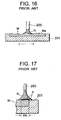
- FIG. 15 is a process diagram showing an example of a wafer flattening process of the related art.
- reference numeral 100 is a chemical mechanical polishing (CMP) apparatus
- reference numeral 200 is a plasma etching apparatus.
- CMP chemical mechanical polishing
- a wafer W held and pressed by a carrier 101 is made to rotate in an opposite direction to a rotating platen 102 to chemically mechanically polish the surface Wa of the wafer W to a mirror surface by a polishing pad 102a of the platen 102.
- the wafer W is conveyed to the plasma etching apparatus 200 where the surface Wa is turned upward and the wafer W held by a holder 201.
- ion or radical or other activated species gas G produced in a plasma generator 202 is sprayed from a nozzle 203 to the surface Wa of the wafer W to locally etch a portion of the surface Wa thicker than the reference thickness value (hereinafter referred to as a "relatively thick portion").
- the holder 201 is made to move to position where the nozzle 203 directly above a relatively thick portion of the wafer W and locally etch the relatively thick portion by the activated species gas G from the nozzle 203 to further flatten the surface Wa.
- the activated species gas G sprayed from the nozzle 203 is a fluid and etches a substance by a chemical reaction with that substance. Accordingly, if the conditions of the region of spraying of the activated species gas G differ, the amount of etching of the substance also changes.
- the present invention was made to solve the above problems and has as its object to provide a wafer flattening process designed to flatten the entire surface of the wafer to a higher precision by projecting the fall in the etching rate at the outer peripheral portion of the wafer and forming the outer peripheral portion of the wafer thinner in advance before plasma etching the entire surface of the wafer, a wafer flattening system, and a wafer flattened by the same.
- a wafer flattening process comprising: an outer peripheral portion processing step for processing the outer peripheral portion of the wafer so that a maximum thickness at a predetermined width of the outer peripheral portion of the wafer surface becomes not more than a minimum thickness at a portion inside from the outer peripheral portion; and a plasma etching step for locally etching a relatively thick portion by spraying plasma activated species gas from a nozzle of a predetermined diameter of opening toward the corresponding relatively thick portion of the wafer surface after the outer peripheral portion processing step.
- the outer peripheral portion processed in the outer peripheral portion processing step may be any width, but as an optimum example, the width of the outer peripheral portion is substantially the same as the diameter of the opening of the nozzle.
- the outer peripheral portion processing step need only process the outer peripheral portion of the wafer to a predetermined thickness. This may be achieved by various processing methods such as polishing and plasma etching.
- the outer peripheral portion processing step is a polishing step which brings the surface of the wafer held by the carrier into contact with a polishing pad of a rotating platen and makes the pressing force on the outer peripheral portion of the wafer higher than the pressing force on the inside portion so as to polish the outer peripheral portion to a mirror surface.
- the outer peripheral portion processing step is chemical mechanical polishing.
- the outer peripheral portion processing step comprises etching only the outer peripheral portion by spraying an activated species gas from above an etching protection plate toward the entire surface of the wafer.
- the outer peripheral portion processing step etches the outer peripheral portion by arranging a hollow ring member of a shape corresponding to the outer peripheral portion of the wafer facing the outer peripheral portion, supplying the activated species gas into the hollow ring member, and spraying it from a plurality of holes formed at predetermined intervals in the hollow ring member.
- the outer peripheral portion is etched by the activated species gas from a nozzle moving relative to the outer peripheral portion.
- the wafer flattening process of the above aspect of the invention may stand as an invention of a system by using specific apparatuses for executing the different steps.
- a wafer flattening system comprising: an outer peripheral portion processing apparatus for processing the outer peripheral portion of a wafer by polishing or plasma etching so that a maximum thickness at a predetermined width of the outer peripheral portion of the wafer surface becomes not more than a minimum thickness at a portion inside from the outer peripheral portion; and a plasma etching apparatus having a holder carrying a wafer processed at the outer peripheral portion processing apparatus, a plasma generator generating a plasma, a nozzle having an opening of a diameter substantially the same as the width of the outer peripheral portion and spraying activated species gas generated at the plasma generator toward the wafer surface, and a moving mechanism for moving the nozzle relative to a predetermined position on the wafer surface.
- the outer peripheral portion processing apparatus is a chemical mechanical polishing apparatus comprising: a platen having a surface as a whole with a polishing pad formed recessed deepest at the center portion of rotation; a carrier for bringing the surface of the held wafer into contact with the polishing pad of the platen, and a rotary drive mechanism for making the platen; and the carrier rotate in mutually opposite directions.
- the outer peripheral portion processing apparatus is a plasma etching apparatus comprising: a holder for carrying the wafer; a protection plate carrying mechanism for placing an etching protection plate on the wafer surface except for the outer peripheral portion of the wafer carried on the holder; a plasma generator for generating plasma; and a nozzle for spraying an activated species gas generated in the plasma generator from above the etching protection plate to the entire surface of the wafer.
- the outer peripheral portion processing apparatus is a plasma etching apparatus comprising: a holder for carrying the wafer; a hollow ring member shaped corresponding to the outer peripheral portion of the wafer, having a plurality of holes formed at predetermined intervals, and arranged facing the outer peripheral portion; and a plasma generator for generating plasma, and supplying the generated activated species gas to the inside of the hollow ring member.
- a wafer with an outer peripheral portion processed so that the maximum thickness at a relatively thick portion remaining at a predetermined width of the outer peripheral portion of the surface becomes not more than a minimum thickness at a portion inside from the outer peripheral portion.
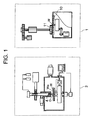
- FIG. 1 is a view of the configuration of a wafer flattening system according to a first embodiment of the present invention.
- the wafer flattening system is provided with a CMP apparatus 1 serving as the outer peripheral portion processing apparatus and a plasma etching apparatus 2.
- the CMP apparatus 1 is an apparatus for polishing the outer peripheral portion of the surface of the wafer W to a predetermined thickness.
- FIG. 2 is a partially cutaway front view of the CMP apparatus.
- the CMP apparatus is an apparatus of substantially the same structure as a general CMP apparatus and is provided with a platen 10 having a polishing pad 10a attached to its surface, a carrier 11, and a rotary drive mechanism 12 for making the platen 10 and the carrier 11 rotate in mutually opposite directions by a main motor 12a and a motor 12b.
- the platen 10 is driven to rotate by the main motor 12a of the rotary drive mechanism 12. That is, the rotation of the main motor 12a is transmitted to a pulley 12c, the rotation of the pulley 12d is converted in speed by a transmission 12e and transmitted to an output shaft 12f, and the platen 10 is rotated at a predetermined speed.
- the platen 10 has distinctive characteristics in its surface shape.
- FIG. 3 is a sectional view of the platen 10.
- the surface of the platen 10 is formed to be deepest at the center of rotation and to become shallower the further toward the outer edge and forms a recessed sectional shape as a whole.
- the carrier 11 is a device for pressing the wafer W by a predetermined pressure to the polishing pad 10a of the platen 10 and has a recessed portion 11a for holding the wafer W at its bottom surface.
- the carrier 11 is attached to the lower end portion of a piston rod 13a of a cylinder 13 and rises or descends by driving the cylinder. Further, a gear 12g attached to the shaft of the motor 12b of the rotary drive mechanism 12 is engaged with a gear 13b of an upper end of the piston rod 13a passing through the cylinder 13.
- the plasma etching apparatus 2 is a general apparatus for locally etching and flattening the wafer W processed by the CMP apparatus 1.
- FIG. 4 is a schematic sectional view of the structure of the plasma etching apparatus.
- the plasma etching apparatus 2 is provided with a plasma generator 3, a nozzle 4, an X-Y drive mechanism 5 as a moving mechanism, and a holder 6.
- the plasma generator 3 is a portion for generating an activated species gas G by plasma discharge and is comprised of a quartz discharge tube 31 affixed to an upper part of a chamber 20, a waveguide 32 attached to the outside of the quartz discharge tube 31, a microwave generator 33 for generating a predetermined microwave to the waveguide 32, and containers 34 and 35 connected through a supply tube 34a to the quartz discharge tube 31.
- the nozzle 4 is formed at a lower end portion of the quartz discharge tube 31 positioned in the chamber 20.
- the activated species gas G generated by the plasma generator 3 is sprayed from the opening 40 to the wafer W side.
- the X-Y drive mechanism 5 is a mechanism for moving the holder 6 in the X-Y directions (left-right and front-back directions in figure) and is controlled by a controller 50.
- the X-Y drive mechanism 5 has connected to it a Z-drive mechanism 51 for making the X-Y drive mechanism 5 as a whole ascend and descend in the Z-direction (up-down direction in the figure).
- the holder 6 moves up and down integrally with the X-Y drive mechanism 5 under the control of the controller 50.
- the holder 6 is a member for holding the wafer W and as explained above is supported by the X-Y drive mechanism 5.
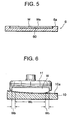
- FIG. 5 is a sectional view of the holder 6.
- the holder 6 is formed by aluminum etc. and has formed at its upper side a holding hole 60 for holding the wafer W.
- the depth of the holding hole 60 is set equal to the thickness of the wafer W.
- the surface Wa of the held wafer W and the upper surface 6a of the holder 6 become substantially the same plane.
- reference numerals 21 and 22 are vacuum pumps.
- the air inside the chamber 20 exhausts the products of the reaction between the activated species gas G and the wafer W to the outside of the chamber 20.
- the outer peripheral portion processing step is executed at the CMP apparatus 1 shown in FIG. 1 and FIG. 2.
- the main motor 12a of the rotary drive mechanism 12 shown in FIG. 2 is driven to make the platen 10 rotate, the motor 12b is driven to make the carrier 11 rotate in the opposite direction from the platen 10 while pressing the carrier 11 holding the wafer W in the recessed portion 11a on the polishing pad 10a by the cylinder 13, and a predetermined slurry is supplied between the wafer W and the polishing pad 10a. This being so, the outer peripheral portion of the wafer W is polished more than the other portions.
- FIG. 6 is a sectional view showing the state of polishing of the outer peripheral portion of the wafer more specifically.
- the polishing rate of the outer peripheral portion Wb of the rotating wafer W becomes higher than that of the inside portion Wc and the outer peripheral portion Wb of the wafer W is polished to become thinner than the inside portion Wc.
- the pressing force on the carrier 11 is adjusted so that the width of the outer peripheral portion Wb becomes substantially equal to the diameter of the opening 40 of the nozzle 4 at the plasma etching apparatus 2.
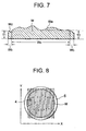
- the wafer W is polished until the outer peripheral portion Wb of the wafer W becomes a predetermined thickness. Specifically, as shown in FIG. 7, it is polished so that the thickness T1 of the relatively thick portion Wd having the greatest thickness in the relatively thick portions existing at the outer peripheral portion Wb becomes not more than the thickness T2 of the portion of the inside portion Wc having the smallest thickness.
- the thickness T1 of the relatively thick portion Wd having the greatest thickness in the relatively thick portions existing at the outer peripheral portion Wb becomes not more than the thickness T2 of the portion of the inside portion Wc having the smallest thickness.
- TTV of the wafer W as a whole is made about 1.53 ⁇ m.
- the outer peripheral portion processing step is executed by the CMP apparatus 1 in this way to polish the outer peripheral portion Wb of the wafer W to a predetermined thickness, then the plasma etching step is executed by the plasma etching apparatus 2.
- the holder 6 is made to move in a zig-zag in the X-Y direction by the X-Y drive mechanism 5. Then, as shown in FIG. 8, the nozzle 4 scans the overall surface Wa of the wafer W relatively in a zig-zag pattern.
- the relative speed is made slower to match the thickness value of the relatively thick portion under the control of the controller 50 and the relatively thick portion is locally etched flat.
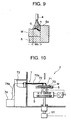
- This etching operation is performed over the wafer W as a whole, but as shown in FIG. 9, when the nozzle 4 arrives directly above the outer peripheral portion Wb, the reaction product A generated by the chemical reaction between the activated species gas G and the upper surface 6a of the holder 6 deposits covering the surface of the outer peripheral portion Wb and inhibits the etching of the outer peripheral portion Wb.
- the relatively thick portion present at the inside portion Wc of the wafer W is etched to substantially the same thickness as the portion having the minimum thickness of the inside portion Wc, the thickness of the inside portion Wc and the thickness of the outer peripheral portion Wb as a whole becomes substantially equal and the TTV of the wafer W is improved.
- the present inventors were actually able to obtain a high quality wafer W of a TTV of 0.39 ⁇ m by polishing the outer peripheral portion Wb of a wafer W of 200 mm by the CMP apparatus 1 and then etching the wafer W given a TTV of 1.53 ⁇ m by the plasma etching apparatus 2 as explained above.
- FIG. 10 is a schematic sectional view of the essential portions of a plasma etching apparatus constituting a wafer flattening system according to a second embodiment of the present invention.
- This embodiment differs from the first embodiment explained above in the point of configuring the outer peripheral portion processing apparatus using the plasma etching apparatus 2 and not using the CMP apparatus 1.
- the plasma etching apparatus 2 is provided with the protection plate carrying mechanism 7.
- the protection plate carrying apparatus 7 is a mechanism for placing the etching protection plate 70 on the inside portion Wc of the wafer W held in the holder 6 and is provided with an arm 72 having a suction pad 71 at the lower side of its front end, a pad mover 73, and an air pump 74.
- the etching protection plate 70 is a dish member having a diameter set to substantially the same as the diameter of the inside portion Wc of the wafer W.
- the arm 72 has a hollow portion 72a communicated with the inside portion of the suction pad 71.
- the pad mover 73 is structured to extend its arm 72 out to the holder 6 side or retract the arm 72 to the pad mover 73 side.
- the air pump 74 is a device for sucking out the air in the suction pad 71 or sending air into the suction pad 71.
- a tube 74a is connected to the hollow portion 72a of the arm 72.
- FIGS. 11A to 11C are process diagrams of the outer peripheral portion processing step.
- the Z-drive mechanism 51 makes the holder 6 holding the wafer W descend together with the X-Y drive mechanism 5, while the pad mover 73 of the protection plate carrying mechanism 7 makes the arm 72 holding the etching protection plate 70 by suction extend out to directly above the wafer W as shown by the two-dot dash line.
- the Z-drive mechanism 51 makes the holder 6 ascend together with the X-Y drive mechanism 5, stops the rise of the holder 6 at the point where the etching protection plate 70 contacts the inside portion Wc of the wafer W, and releases the suction force of the suction pad 71 on the etching protection plate 70 by the air pump 74.
- the etching protection plate 70 is placed on the inside portion Wc and only the outer peripheral portion Wb is exposed.
- the arm 72 is pulled in to the pad mover 73 side and the holder 6 is made to descent together with the X-Y drive mechanism 5.
- the etching protection plate 70 since the inside portion Wc of the wafer W is covered by the etching protection plate 70, only the outer peripheral portion Wb is etched by the activated species gas G.
- the activated species gas G is sprayed on the wafer W until the outer peripheral portion Wb becomes the above predetermined thickness, then the holder 6 is made to ascend and the arm 72 is extended to pick up the etching protection plate 70 by suction by the suction pad 71.
- the outer peripheral portion processing step is completed by pulling in the arm 72 holding the etching protection plate 70 by suction to the pad mover 73 side.
- the surface Wa of the wafer W is etched in the same way as the above first embodiment in that state.
- FIG. 12 is a schematic sectional view of the structure of a plasma etching apparatus constituting the wafer flattening system according to a third embodiment of the present invention.
- This embodiment is similar to the above second embodiment in the point that the outer peripheral portion processing apparatus is configured using the plasma etching apparatus 2, but differs from the second embodiment in the point that the structure of the outer peripheral portion processing apparatus is simplified.
- reference numeral 8 is a hollow ring member 8 and is connected to the lower end of a conduct 81 branched from the quartz discharge tube 31.
- FIG. 13 is a plan view showing the hollow ring member 8 from the bottom.
- the hollow ring member 8 forms a disk as a whole and has an outer diameter and thickness set to be substantially equal in outer shape to the outer diameter of the wafer W and the width of the outer peripheral portion Wb.
- a plurality of holes 80 are made at predetermined intervals in the bottom surface of the hollow ring member 8.
- This hollow ring member 8 as shown in FIG. 12, is arranged to face the outer peripheral portion Wb of the wafer W and is supported by the conduit 81.
- the conduit 81 communicates with the inside of the hollow ring member 8 through a lower opening.
- a valve 82 is interposed at its horizontal portion.
- valve 36 similar to the valve 82 is interposed in the quartz discharge tube 31. By operating these valves 36 and 82, it becomes possible to spray the activated species gas G from either of the nozzle 4 or holes 80 of the hollow ring member 8.
- the holder used in this embodiment is a disk-shaped holder 6'.
- the wafer W is placed on and affixed to the holder 6'.
- valve 82 is opened in the state with the valve 36 closed and the activated species gas G generated in the plasma generator 3 (see FIG. 4) is supplied into the conduit 81.
- the activated species gas G in the conduit 81 reaches the inside of the hollow ring member 8 and is sprayed from the plurality of holes 80 at the bottom surface toward the outer peripheral portion Wb of the wafer W.
- the outer peripheral portion Wb can be etched to the above predetermined thickness.
- the valve 82 When executing the plasma etching step, the valve 82 is closed, then the valve 36 is opened and the activated species gas G is sprayed from the nozzle 4. Further, in the same way as the first embodiment explained above, the surface Wa of the wafer W is etched by the activated species gas G of the nozzle 4 while moving the holder 6 by the X-Y drive mechanism 5.
- the structure of the outer peripheral portion processing apparatus itself is simple, so it is possible to further slash the cost of the facilities.
- the nozzle 4 was fixed in place and the wafer W was made to move by the X-Y drive mechanism 5 to move the nozzle to a predetermined location of the surface Wa of the wafer W, but it is also possible to fix the wafer W in place and make the nozzle 4 to move.
- the explanation was given of a plasma generator 3 generating an activated species gas G using microwaves, but the plasma generator 3 need only be able to produce activated species gas G and is not limited to this.
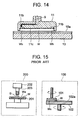
- the surface of the platen 10 of the CMP apparatus 1 was formed recessed to execute the outer peripheral portion processing step, but it is also possible to use the carrier 11 shown in FIG. 14 and execute the outer peripheral portion processing step by a flat surface platen 10.
- a ring-shaped pressure chamber 11b opening to the recessed portion 11a side is cut into a location at the bottom surface of the carrier 11 corresponding to the outer peripheral portion Wb of the wafer W and a film 11c is adhered over the entire lower surface of the carrier 11.
- air of a predetermined pressure may be supplied into the pressure chamber 11b through the air hose 9 of a not shown air pump to make the pressing force on the outer peripheral portion Wb larger than the pressing force on the inside portion Wc and as a result polish the outer peripheral portion Wb to the above predetermined thickness.
- the explanation was made of configurations for etching the outer peripheral portion Wb of the wafer W using an etching protection plate 70 or hollow ring member 8, but it is also possible to make the holder 6 rotate by the X-Y drive mechanism 5 of the plasma etching apparatus 2 to make the nozzle 4 spraying the activated species gas G move relatively along the outer peripheral portion Wb of the wafer W and thereby etching only the outer peripheral portion Wb.
Landscapes
- Engineering & Computer Science (AREA)
- Mechanical Engineering (AREA)
- Mechanical Treatment Of Semiconductor (AREA)
- Drying Of Semiconductors (AREA)
- ing And Chemical Polishing (AREA)
Applications Claiming Priority (2)
| Application Number | Priority Date | Filing Date | Title |
|---|---|---|---|
| JP12668198 | 1998-04-21 | ||
| JP10126681A JPH11302878A (ja) | 1998-04-21 | 1998-04-21 | ウエハ平坦化方法,ウエハ平坦化システム及びウエハ |
Publications (2)
| Publication Number | Publication Date |
|---|---|
| EP0951963A2 true EP0951963A2 (fr) | 1999-10-27 |
| EP0951963A3 EP0951963A3 (fr) | 2003-08-06 |
Family
ID=14941231
Family Applications (1)
| Application Number | Title | Priority Date | Filing Date |
|---|---|---|---|
| EP99102810A Withdrawn EP0951963A3 (fr) | 1998-04-21 | 1999-02-25 | Procédé de lissage de plaquette semiconductrice, dispositif de lissage de plaquette semiconductrice, et plaquette semiconductrice |
Country Status (3)
| Country | Link |
|---|---|
| US (1) | US6254718B1 (fr) |
| EP (1) | EP0951963A3 (fr) |
| JP (1) | JPH11302878A (fr) |
Cited By (4)
| Publication number | Priority date | Publication date | Assignee | Title |
|---|---|---|---|---|
| WO2002001617A1 (fr) * | 2000-06-29 | 2002-01-03 | Shin-Etsu Handotai Co.,Ltd. | Procede de traitement d'une plaquette de semi-conducteur et appareil de gravure au plasma |
| EP1004401A3 (fr) * | 1998-11-26 | 2002-01-23 | Speedfam Co.,Ltd. | Dispositif de polissage pour semiconducteurs |
| WO2002011198A3 (fr) * | 2000-07-28 | 2002-04-11 | Advanced Micro Devices Inc | Procede et dispositif permettant de commander l'uniformite d'une plaquette dans un outil de polissage mecanique et chimique a l'aide de signatures de tetes de support |
| WO2008149735A1 (fr) * | 2007-06-05 | 2008-12-11 | Asahi Glass Co., Ltd. | Procédé de traitement d'une surface de substrat de verre |
Families Citing this family (12)
| Publication number | Priority date | Publication date | Assignee | Title |
|---|---|---|---|---|
| JP3871433B2 (ja) * | 1998-03-10 | 2007-01-24 | スピードファム株式会社 | ウエハ平坦化方法及び記録媒体 |
| US6451217B1 (en) * | 1998-06-09 | 2002-09-17 | Speedfam-Ipec Co., Ltd. | Wafer etching method |
| JP2006011434A (ja) * | 2002-03-29 | 2006-01-12 | Hoya Corp | マスクブランク用基板、マスクブランクおよび転写用マスクの製造方法 |
| US20040157461A1 (en) * | 2003-02-10 | 2004-08-12 | Seh America, Inc. | Method for fabricating a wafer including dry etching the edge of the wafer |
| WO2012042292A1 (fr) | 2010-09-30 | 2012-04-05 | Freescale Semiconductor, Inc. | Procédés de traitement de tranche de semi-conducteur, tranche de semi-conducteur et dispositif à semi-conducteur |
| US9174323B2 (en) * | 2012-11-07 | 2015-11-03 | Intermolecular, Inc. | Combinatorial tool for mechanically-assisted surface polishing and cleaning |
| JP6129551B2 (ja) * | 2012-12-27 | 2017-05-17 | 株式会社ディスコ | 板状物の加工方法 |
| JP2019201149A (ja) * | 2018-05-17 | 2019-11-21 | 東京エレクトロン株式会社 | 基板処理装置及び基板処理方法 |
| CN109623581A (zh) * | 2019-01-04 | 2019-04-16 | 芜湖启迪半导体有限公司 | 一种硬质材料的表面抛光方法 |
| JP7412142B2 (ja) * | 2019-11-13 | 2024-01-12 | 株式会社ディスコ | ウェーハの加工方法 |
| CN112095107A (zh) * | 2020-10-19 | 2020-12-18 | 东莞市万业实业有限公司 | 等离子电浆抛光挂具自动翻转装置及其翻转方法 |
| JP2024039841A (ja) * | 2022-09-12 | 2024-03-25 | キオクシア株式会社 | プラズマ処理装置、プラズマ処理方法、および半導体装置の製造方法 |
Family Cites Families (13)
| Publication number | Priority date | Publication date | Assignee | Title |
|---|---|---|---|---|
| US5254830A (en) * | 1991-05-07 | 1993-10-19 | Hughes Aircraft Company | System for removing material from semiconductor wafers using a contained plasma |
| US5291415A (en) * | 1991-12-13 | 1994-03-01 | Hughes Aircraft Company | Method to determine tool paths for thinning and correcting errors in thickness profiles of films |
| IL104268A0 (en) * | 1992-01-31 | 1993-05-13 | Hughes Aircraft Co | Reactive gas for plasma assisted chemical etching and methods for stable plasma etching of substrates over edges |
| GB2272225B (en) * | 1992-10-06 | 1996-07-17 | Balzers Hochvakuum | A method for masking a workpiece and a vacuum treatment facility |
| TW273067B (fr) * | 1993-10-04 | 1996-03-21 | Tokyo Electron Co Ltd | |
| JPH07297195A (ja) * | 1994-04-27 | 1995-11-10 | Speedfam Co Ltd | 半導体装置の平坦化方法及び平坦化装置 |
| JPH07328916A (ja) * | 1994-06-06 | 1995-12-19 | Japan Aviation Electron Ind Ltd | ラップ・ポリッシュ盤 |
| US5968849A (en) * | 1995-06-26 | 1999-10-19 | Motorola, Inc. | Method for pre-shaping a semiconductor substrate for polishing and structure |
| JPH0927482A (ja) | 1995-07-11 | 1997-01-28 | Speedfam Co Ltd | プラズマエッチング装置 |
| US5718618A (en) * | 1996-02-09 | 1998-02-17 | Wisconsin Alumni Research Foundation | Lapping and polishing method and apparatus for planarizing photoresist and metal microstructure layers |
| JPH09234667A (ja) * | 1996-02-29 | 1997-09-09 | Komatsu Electron Metals Co Ltd | 半導体ウェハの研磨方法 |
| JP3620554B2 (ja) * | 1996-03-25 | 2005-02-16 | 信越半導体株式会社 | 半導体ウェーハ製造方法 |
| JPH10235552A (ja) * | 1997-02-24 | 1998-09-08 | Ebara Corp | ポリッシング装置 |
-
1998
- 1998-04-21 JP JP10126681A patent/JPH11302878A/ja active Pending
-
1999
- 1999-02-25 EP EP99102810A patent/EP0951963A3/fr not_active Withdrawn
- 1999-03-01 US US09/260,336 patent/US6254718B1/en not_active Expired - Fee Related
Cited By (5)
| Publication number | Priority date | Publication date | Assignee | Title |
|---|---|---|---|---|
| EP1004401A3 (fr) * | 1998-11-26 | 2002-01-23 | Speedfam Co.,Ltd. | Dispositif de polissage pour semiconducteurs |
| WO2002001617A1 (fr) * | 2000-06-29 | 2002-01-03 | Shin-Etsu Handotai Co.,Ltd. | Procede de traitement d'une plaquette de semi-conducteur et appareil de gravure au plasma |
| WO2002011198A3 (fr) * | 2000-07-28 | 2002-04-11 | Advanced Micro Devices Inc | Procede et dispositif permettant de commander l'uniformite d'une plaquette dans un outil de polissage mecanique et chimique a l'aide de signatures de tetes de support |
| US6592429B1 (en) | 2000-07-28 | 2003-07-15 | Advanced Micro Devices, Inc. | Method and apparatus for controlling wafer uniformity in a chemical mechanical polishing tool using carrier head signatures |
| WO2008149735A1 (fr) * | 2007-06-05 | 2008-12-11 | Asahi Glass Co., Ltd. | Procédé de traitement d'une surface de substrat de verre |
Also Published As
| Publication number | Publication date |
|---|---|
| JPH11302878A (ja) | 1999-11-02 |
| EP0951963A3 (fr) | 2003-08-06 |
| US6254718B1 (en) | 2001-07-03 |
Similar Documents
| Publication | Publication Date | Title |
|---|---|---|
| US6254718B1 (en) | Combined CMP and plasma etching wafer flattening system | |
| US6354923B1 (en) | Apparatus for planarizing microelectronic substrates and conditioning planarizing media | |
| US6494774B1 (en) | Carrier head with pressure transfer mechanism | |
| JP4427191B2 (ja) | 化学機械研磨用可撓メンブレン付キャリアヘッド | |
| US6120354A (en) | Method of chemical mechanical polishing | |
| US20040192173A1 (en) | Carrier head with flexible membrane to provide controllable pressure and loading area | |
| US20040108062A1 (en) | Method and apparatus for supporting a microelectronic substrate relative to a planarization pad | |
| US7121934B2 (en) | Carrier head for chemical mechanical polishing apparatus | |
| JPH0621029A (ja) | 半導体ウェハの化学的−機械的研磨装置およびそれを用いた方法 | |
| JP2000036488A (ja) | ウエハ平坦化方法及びそのシステム | |
| JP2004501779A (ja) | エッジ圧力制御付きキャリアヘッド | |
| CN101499412A (zh) | 基板处理装置及基板处理方法 | |
| JPH10217112A (ja) | Cmp装置 | |
| KR100636455B1 (ko) | 화학 기계적 연마를 위한 제어가능한 압력 및 부하 영역을갖는 캐리어 헤드 | |
| JP2000190211A (ja) | 化学的機械的研磨装置および方法 | |
| US20020037684A1 (en) | Dry chemical-mechanical polishing method | |
| JPH11285966A (ja) | キャリア及びcmp装置 | |
| CN100364720C (zh) | 在化学机械抛光过程中抛光晶片的方法和携载头 | |
| JPH09171980A (ja) | 半導体装置の製造方法 | |
| JP3814558B2 (ja) | 局所ドライエッチング方法及び半導体ウェハ表面の位置−厚さデータの処理方法 | |
| JP2000033555A (ja) | 研磨装置 | |
| JP2002231700A (ja) | ナノトポグラフィ除去方法 | |
| KR101001312B1 (ko) | 초음파 세정 장치 | |
| JP2003163193A (ja) | ウェーハ研磨方法および研磨ヘッド | |
| JP2000082688A (ja) | 半導体ウェーハのノッチ部のアール面取り方法およびその装置 |
Legal Events
| Date | Code | Title | Description |
|---|---|---|---|
| PUAI | Public reference made under article 153(3) epc to a published international application that has entered the european phase |
Free format text: ORIGINAL CODE: 0009012 |
|
| AK | Designated contracting states |
Kind code of ref document: A2 Designated state(s): AT BE CH CY DE DK ES FI FR GB GR IE IT LI LU MC NL PT SE |
|
| AX | Request for extension of the european patent |
Free format text: AL;LT;LV;MK;RO;SI |
|
| PUAL | Search report despatched |
Free format text: ORIGINAL CODE: 0009013 |
|
| 17P | Request for examination filed |
Effective date: 20030514 |
|
| AK | Designated contracting states |
Designated state(s): AT BE CH CY DE DK ES FI FR GB GR IE IT LI LU MC NL PT SE |
|
| AX | Request for extension of the european patent |
Extension state: AL LT LV MK RO SI |
|
| STAA | Information on the status of an ep patent application or granted ep patent |
Free format text: STATUS: THE APPLICATION HAS BEEN WITHDRAWN |
|
| 18W | Application withdrawn |
Effective date: 20040129 |