EP0944191A1 - Method for optical fiber communication, and device and system for use in carrying out the method - Google Patents
Method for optical fiber communication, and device and system for use in carrying out the method Download PDFInfo
- Publication number
- EP0944191A1 EP0944191A1 EP99102790A EP99102790A EP0944191A1 EP 0944191 A1 EP0944191 A1 EP 0944191A1 EP 99102790 A EP99102790 A EP 99102790A EP 99102790 A EP99102790 A EP 99102790A EP 0944191 A1 EP0944191 A1 EP 0944191A1
- Authority
- EP
- European Patent Office
- Prior art keywords
- optical
- signal
- transmission line
- bit error
- optical fiber
- Prior art date
- Legal status (The legal status is an assumption and is not a legal conclusion. Google has not performed a legal analysis and makes no representation as to the accuracy of the status listed.)
- Ceased
Links
Images


Classifications
-
- H—ELECTRICITY
- H04—ELECTRIC COMMUNICATION TECHNIQUE
- H04B—TRANSMISSION
- H04B10/00—Transmission systems employing electromagnetic waves other than radio-waves, e.g. infrared, visible or ultraviolet light, or employing corpuscular radiation, e.g. quantum communication
- H04B10/25—Arrangements specific to fibre transmission
- H04B10/2507—Arrangements specific to fibre transmission for the reduction or elimination of distortion or dispersion
- H04B10/2513—Arrangements specific to fibre transmission for the reduction or elimination of distortion or dispersion due to chromatic dispersion
- H04B10/2525—Arrangements specific to fibre transmission for the reduction or elimination of distortion or dispersion due to chromatic dispersion using dispersion-compensating fibres
-
- G—PHYSICS
- G02—OPTICS
- G02F—OPTICAL DEVICES OR ARRANGEMENTS FOR THE CONTROL OF LIGHT BY MODIFICATION OF THE OPTICAL PROPERTIES OF THE MEDIA OF THE ELEMENTS INVOLVED THEREIN; NON-LINEAR OPTICS; FREQUENCY-CHANGING OF LIGHT; OPTICAL LOGIC ELEMENTS; OPTICAL ANALOGUE/DIGITAL CONVERTERS
- G02F1/00—Devices or arrangements for the control of the intensity, colour, phase, polarisation or direction of light arriving from an independent light source, e.g. switching, gating or modulating; Non-linear optics
- G02F1/01—Devices or arrangements for the control of the intensity, colour, phase, polarisation or direction of light arriving from an independent light source, e.g. switching, gating or modulating; Non-linear optics for the control of the intensity, phase, polarisation or colour
- G02F1/0121—Operation of devices; Circuit arrangements, not otherwise provided for in this subclass
- G02F1/0123—Circuits for the control or stabilisation of the bias voltage, e.g. automatic bias control [ABC] feedback loops
-
- H—ELECTRICITY
- H04—ELECTRIC COMMUNICATION TECHNIQUE
- H04B—TRANSMISSION
- H04B10/00—Transmission systems employing electromagnetic waves other than radio-waves, e.g. infrared, visible or ultraviolet light, or employing corpuscular radiation, e.g. quantum communication
- H04B10/07—Arrangements for monitoring or testing transmission systems; Arrangements for fault measurement of transmission systems
- H04B10/075—Arrangements for monitoring or testing transmission systems; Arrangements for fault measurement of transmission systems using an in-service signal
- H04B10/077—Arrangements for monitoring or testing transmission systems; Arrangements for fault measurement of transmission systems using an in-service signal using a supervisory or additional signal
- H04B10/0775—Performance monitoring and measurement of transmission parameters
-
- H—ELECTRICITY
- H04—ELECTRIC COMMUNICATION TECHNIQUE
- H04B—TRANSMISSION
- H04B10/00—Transmission systems employing electromagnetic waves other than radio-waves, e.g. infrared, visible or ultraviolet light, or employing corpuscular radiation, e.g. quantum communication
- H04B10/07—Arrangements for monitoring or testing transmission systems; Arrangements for fault measurement of transmission systems
- H04B10/075—Arrangements for monitoring or testing transmission systems; Arrangements for fault measurement of transmission systems using an in-service signal
- H04B10/079—Arrangements for monitoring or testing transmission systems; Arrangements for fault measurement of transmission systems using an in-service signal using measurements of the data signal
- H04B10/0795—Performance monitoring; Measurement of transmission parameters
- H04B10/07953—Monitoring or measuring OSNR, BER or Q
-
- H—ELECTRICITY
- H04—ELECTRIC COMMUNICATION TECHNIQUE
- H04B—TRANSMISSION
- H04B10/00—Transmission systems employing electromagnetic waves other than radio-waves, e.g. infrared, visible or ultraviolet light, or employing corpuscular radiation, e.g. quantum communication
- H04B10/07—Arrangements for monitoring or testing transmission systems; Arrangements for fault measurement of transmission systems
- H04B10/075—Arrangements for monitoring or testing transmission systems; Arrangements for fault measurement of transmission systems using an in-service signal
- H04B10/079—Arrangements for monitoring or testing transmission systems; Arrangements for fault measurement of transmission systems using an in-service signal using measurements of the data signal
- H04B10/0799—Monitoring line transmitter or line receiver equipment
-
- G—PHYSICS
- G02—OPTICS
- G02F—OPTICAL DEVICES OR ARRANGEMENTS FOR THE CONTROL OF LIGHT BY MODIFICATION OF THE OPTICAL PROPERTIES OF THE MEDIA OF THE ELEMENTS INVOLVED THEREIN; NON-LINEAR OPTICS; FREQUENCY-CHANGING OF LIGHT; OPTICAL LOGIC ELEMENTS; OPTICAL ANALOGUE/DIGITAL CONVERTERS
- G02F2203/00—Function characteristic
- G02F2203/25—Frequency chirping of an optical modulator; Arrangements or methods for the pre-set or tuning thereof
-
- H—ELECTRICITY
- H04—ELECTRIC COMMUNICATION TECHNIQUE
- H04B—TRANSMISSION
- H04B2210/00—Indexing scheme relating to optical transmission systems
- H04B2210/07—Monitoring an optical transmission system using a supervisory signal
- H04B2210/077—Monitoring an optical transmission system using a supervisory signal using a separate fibre
-
- H—ELECTRICITY
- H04—ELECTRIC COMMUNICATION TECHNIQUE
- H04B—TRANSMISSION
- H04B2210/00—Indexing scheme relating to optical transmission systems
- H04B2210/25—Distortion or dispersion compensation
- H04B2210/252—Distortion or dispersion compensation after the transmission line, i.e. post-compensation
-
- H—ELECTRICITY
- H04—ELECTRIC COMMUNICATION TECHNIQUE
- H04B—TRANSMISSION
- H04B2210/00—Indexing scheme relating to optical transmission systems
- H04B2210/25—Distortion or dispersion compensation
- H04B2210/254—Distortion or dispersion compensation before the transmission line, i.e. pre-compensation
Definitions
- the present invention relates generally to compensation for chromatic dispersion and nonlinearity in an optical fiber, and more particularly to a method for optical fiber communication which can compensate for chromatic dispersion and nonlinearity in an optical fiber, and a device and system for use in carrying out the method.
- optical fiber communication systems each using such an optical fiber as a transmission line have been put to practical use.
- the optical fiber itself has a very wide band.
- a transmission capacity by the optical fiber is actually limited by a system design.
- the most important limitation is due to waveform distortion by chromatic dispersion occurring in the optical fiber.
- the optical fiber attenuates an optical signal at a rate of about 0.2 dB/km, for example. Loss of the optical signal due to this attenuation has been compensated for by adopting an optical amplifier such as an erbium doped fiber amplifier (EDFA) which is a typical example.
- the EDFA has a gain band in a 1.55 ⁇ m band where a silica optical fiber gives a lowest loss.
- the chromatic dispersion that is often referred to simply as dispersion is a phenomenon such that the group velocity of an optical signal in an optical fiber changes as a function of the wavelength (or frequency) of the optical signal.
- an optical signal having a longer wavelength propagates faster than an optical signal having a shorter wavelength in a wavelength region shorter than 1.3 ⁇ m, and the resultant dispersion is usually referred to as normal dispersion.
- the dispersion (whose unit is ps/nm/km) takes on a negative value.
- an optical signal having a shorter wavelength propagates faster than an optical signal having a longer wavelength in a wavelength region longer than 1.3 ⁇ m, and the resultant dispersion is usually referred to as anomalous dispersion.
- the dispersion takes on a positive value.
- the optical Kerr effect is a phenomenon such that the refractive index of an optical fiber changes with the power of intensity of an optical signal.
- a change in the refractive index modulates the phase of an optical signal propagating in an optical fiber, resulting in the occurrence of frequency chirping which changes a signal spectrum.
- This phenomenon is known as self-phase modulation (SPM).
- SPM self-phase modulation
- the chromatic dispersion and the optical Kerr effect impart waveform distortion to an optical signal with an increase in transmission distance. Accordingly, to allow long-haul transmission by an optical fiber, the chromatic dispersion and the nonlinearity must be controlled, compensated, or suppressed.
- Other objects of the present invention will become apparent from the following description.
- a method for optical fiber communication An optical signal having a chirping determined by a chirp parameter is first output to an optical fiber transmission line.
- the optical signal transmitted by the optical fiber transmission line is next converted into an electrical signal.
- a bit error of the electrical signal is next detected.
- the chirp parameter mentioned above is controlled so that the bit error detected above is reduced.
- the chirp parameter is controlled so that the bit error detected is reduced. Accordingly, a chirping occurring in the optical fiber transmission line can be suppressed by the chirping of the optical signal to be output to the optical fiber transmission line, thereby compensating for chromatic dispersion and nonlinearity.
- the sign of the chirp parameter of the optical signal to be output to the optical fiber transmission line can be switched by switching an operating point of the Mach-Zehnder optical modulator.
- the chirp parameter can be continuously changed according to a bias voltage to be applied to the electroabsorption optical modulator. Accordingly, the chirp parameter can be adjusted to an optimum value so that the bit error detected is minimized.
- the optical signal is generated by optical modulation based on a modulating signal obtained by adding a redundancy code to a transmission data code.
- the bit error of the electrical signal can be corrected according to the redundancy code.
- the bit error of the electrical signal can be detected by counting the number of corrections of the bit error.
- a system comprising first and second terminal devices and an optical fiber transmission line connecting the first and second terminal devices.
- the first terminal device comprises an optical transmitter and a control unit.
- the optical transmitter outputs an optical signal having a chirping determined by a chirp parameter to the optical fiber transmission line.
- the control unit controls the chirp parameter according to a control signal.
- the second terminal device comprises an optical receiver and a monitor unit.
- the optical receiver converts the optical signal transmitted by the optical fiber transmission line into an electrical signal.
- the monitor unit detects a bit error of the electrical signal. Supervisory information on the bit error detected is transmitted back to the first terminal device.
- a terminal device comprising an optical transmitter for outputting an optical signal having a chirping determined by a chirp parameter to an optical fiber transmission line; means for receiving supervisory information on a bit error detected in relation to the optical signal transmitted by the optical fiber transmission line; and means for controlling the chirp parameter according to the supervisory information so that the bit error detected is reduced.
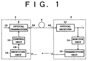
- FIG. 1 is a block diagram showing a preferred embodiment of the system according to the present invention.
- This system includes a first terminal device 2, a second terminal device 4, and an optical fiber transmission line 6 connecting the first and second terminal devices 2 and 4.
- the first terminal device 2 includes an optical transmitter 8 for outputting an optical signal having a chirping determined by a chirp parameter to the optical fiber transmission line 6 from its first end 6A, and a control unit 10 for controlling the chirp parameter in the optical transmitter 8 according to a control signal CS.
- the second terminal device 4 includes an optical receiver 12 for converting the optical signal transmitted by the optical fiber transmission line 6 into an electrical signal, and a monitor unit 14 for detecting a bit error of the electrical signal output from the optical receiver 12.
- the second terminal device 4 further includes a transmitting unit 16 for transmitting supervisory information on the bit error detected to the first terminal device 2.
- the first terminal device 2 further includes a receiving unit 18 for receiving the supervisory information transmitted from the second terminal device 4.
- the receiving unit 18 generates the control signal CS to be supplied to the control unit 10 so that the bit error detected in the monitor unit 14 is reduced, for example.
- the transmission of the supervisory information from the transmitting unit 16 to the receiving unit 18 may be performed by using the optical fiber transmission line 6, by using another optical fiber transmission line not shown, or by means of an electrical circuit or a wireless circuit.
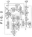
- FIG. 2 is a block diagram showing a preferred embodiment of the first terminal device 2 shown in FIG. 1.
- the optical transmitter 8 includes a light source 20 such as a laser diode for outputting continuous wave (CW) light, an FEC (Forward Error Correction) encoder 22 for generating a modulating signal MS by adding a redundancy code to a transmission data code of an input signal IS, and a Mach-Zehnder optical modulator (MZ modulator) 24 for modulating the CW light output from the light source 20 according to the modulating signal MS to generate an optical signal.
- the optical signal thus generated is output through an optical coupler 26 to the optical fiber transmission line 6.
- FIG. 3 is a block diagram showing a preferred embodiment of the second terminal device 4 shown in FIG. 1.
- the optical receiver 12 includes a photodetector (PD) 28 such as a photodiode for converting the optical signal transmitted by the optical fiber transmission line 6 into an electrical signal, a demodulating circuit 30 for performing demodulation according to the electrical signal output from the photodetector 28, and an FEC decoder 32 for correcting a bit error of the electrical signal output from the demodulating circuit 30 according to the redundancy code added by the FEC encoder 22 (see FIG. 2). Accordingly, the monitor unit 14 can detect the bit error by counting the number of corrections of the bit error in the FEC decoder 32.
- PD photodetector
- FEC decoder 32 for correcting a bit error of the electrical signal output from the demodulating circuit 30 according to the redundancy code added by the FEC encoder 22 (see FIG. 2).
- the monitor unit 14 can detect the bit error by counting the number of corrections of the bit
- the input signal IS input into the FEC encoder 22 and the electrical signal output from the FEC decoder 32 are comply with synchronous digital hierarchy (SDH).
- SDH defines an interface for effectively multiplexing various high-speed services or existing low-speed services, and it was standardized at CCITT (presently, ITU-T) on November, 1988.
- the multiplexing is characterized in that a fundamental rate of 155.52 Mb/s (which is called STM-1 level) is adopted and an integral multiple of this rate, i.e., N ⁇ 155.52 Mb/s, is used as a transmission rate, provided that the frequencies in the network are synchronized.
- N 1, 4, and 16, i.e., 155.52 Mb/s (STM-1), 622.08 Mb/s (STM-4), and 2.48832 Gb/s (STM-16) are defined.
- the FEC decoder 32 (see FIG. 3) outputs transmission data whose bit error has been corrected and also outputs data reflecting the number of corrections of the bit error. Accordingly, the monitor unit 14 counts the number of corrections of the bit error in the FEC decoder 32, thereby easily detecting the degree of the bit error. The number of corrections detected in the monitor unit 14 is transmitted as supervisory information from the transmitting unit 16 to the first terminal device 2.
- optical transmitter 8 The configuration and operation of the optical transmitter 8 and the control unit 10 will now be described in detail with reference to FIG. 2.
- the MZ modulator 24 includes an input port 24A optically connected to the light source 20, an output port 24B optically connected to the optical coupler 26, a pair of optical paths 36 and 38 optically coupled through a Y branch 34 to the input port 24A, and another Y branch 40 for optically coupling the optical paths 36 and 38 to the output port 24B.
- the Y branches 34 and 40 and the optical paths 36 and 38 may be obtained by performing thermal diffusion of Ti or the like with a given pattern on a dielectric substrate formed of LiNbO 3 or the like to thereby form an optical waveguide structure.
- a ground electrode 42 and a signal electrode 44 are provided on the optical paths 36 and 38, respectively, to apply an electric field to the optical paths 36 and 38.
- the signal electrode 44 is provided as a traveling-wave type, for example.
- the CW light supplied from the light source 20 to the input port 24A is first branched at the Y branch 34 into first and second branch beams having the same power.
- the first and second branch beams propagate in the optical paths 36 and 38, respectively, and then joined together at the Y branch 40.
- the electric field generated between the ground electrode 42 and the signal electrode 44 changes the refractive indices of the optical paths 36 and 38 in opposite directions, thereby producing a phase difference between the first and second branch beams.
- the first and second branch beams different in phase interfere with each other at the Y branch 40, so that an optical signal intensity-modulated according to the modulating signal MS is output from the output port 24B.
- the optical transmitter 8 further includes a superimposing circuit 46, a bias circuit 48, a low-pass filter 50, a phase detector 52, an oscillator 54, and a photodetector 56.
- the control circuit 10 in this preferred embodiment includes a chirp parameter setting circuit 58 and two sign inverting circuits 60 and 62.
- a low-frequency signal having a frequency f 0 output from the oscillator 54 is used to stabilize the operating point.
- the low-frequency signal is supplied through the sign inverting circuit 62 to the superimposing circuit 46.
- the modulating signal MS from the FEC encoder 22 is supplied through the sign inverting circuit 60 to the superimposing circuit 46.
- the low-frequency signal is superimposed on the modulating signal MS in the superimposing circuit 46, and a resultant superimposed signal is supplied to the signal electrode 44.
- the superimposing circuit 46 may be configured of a variable-gain amplifier and a capacitor for AC-connecting this amplifier to the signal electrode 44.
- the sign inverting circuits 60 and 62 are controlled by the chirp parameter setting circuit 58. This control will be hereinafter described in detail.
- a bias voltage controlled so as to stabilize the operating point is supplied from the bias circuit 48 to the signal electrode 44.
- a part of the optical signal output from the output port 24B of the MZ modulator 24 is converted into an electrical signal by the photodetector 56.
- This electrical signal may include a low-frequency component having a frequency f 0 .
- the phase detector 52 is provided as a synchronous detector circuit. The phase detector 52 compares the phase of the low-frequency signal from the oscillator 54 and the phase of the low-frequency component from the photodetector 56. The result of this phase comparison appears in a DC component of the output signal from the phase detector 52. Accordingly, the DC component is extracted by the low-pass filter 50 and then fed back to the bias circuit 48. In this feedback loop, the bias circuit 48 controls the bias voltage so that the low-frequency component from the photodetector 56 is minimized.
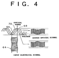
- Reference numeral 64 denotes a waveform of an electrical signal input to the MZ modulator 24.
- An optimum operating point of the MZ modulator 24 is determined by an operating characteristic curve in which the high and low levels of the input electrical signal 64 give maximum and minimum output signal powers, respectively.
- the operating characteristic curve is given by a sine curve showing the relation between optical power and applied voltage.
- a shift of the operating characteristic curve along the voltage axis is referred to as an operating point drift.
- the operating characteristic curve 66 When the operating characteristic curve 66 is shifted to a curve 68 or 70 because of temperature fluctuations or the like, a low-frequency component appears in the output optical signal, and the phase of the low-frequency component reflects a direction of shifting of the curve 66. That is, the phases of the envelopes of the output optical signals given by the operating characteristic curves 68 and 70 are different by 180° from each other. Accordingly, the operating point of the MZ modulator 24 can be stabilized by performing synchronous detection by use of the phase detector 52 as shown in FIG. 2.
- the MZ modulator 24 optical switching by interference is performed, and it is therefore possible to perform prechirping by utilizing wavelength fluctuations (chirping) occurring substantially due to interference.
- the prechirping is a method for suppressing a degradation in transmission waveform due to chromatic dispersion and nonlinear effects in an optical fiber transmission line by preliminarily giving wavelength (frequency) fluctuations within one pulse of an optical signal to be transmitted.
- FIG. 5A there is shown an operating characteristic curve of the MZ modulator 24.
- a positive pulse as shown in the left graph of FIG. 5B is given as the applied voltage by using a region 72 in the vicinity of one stable point Vb1
- the optical power (P) increases with an increase in the applied voltage (V) in the region 72.
- an optical pulse is output with the same polarity as that of the voltage pulse, as shown in the left graph of FIG. 5C.
- the wavelengths at the rising portion of the optical pulse are shorter than the average value, and the wavelengths at the falling portion of the optical pulse are longer than the average value as shown in the left graph of FIG. 5D. That is, the wavelength shifts from shorter wavelengths (blue side) toward longer wavelengths (red side) with respect to time (t) in one optical pulse. This phenomenon is referred to as red shift.
- the optical power (P) decreases with an increase in the applied voltage (V) in the region 74. Accordingly, an optical pulse is output with a polarity opposite to that of the voltage pulse, as shown in the right graph of FIG. 5C.
- the wavelength shifts toward longer wavelengths at the rising portion of the optical pulse and shifts toward shorter wavelengths at the falling portion of the optical pulse as shown in the right graph of FIG. 5D. That is, the wavelength shifts from longer wavelengths (red side) toward shorter wavelengths (blue side) with respect to time (t) in one optical pulse. This phenomenon is referred to as blue shift.
- the wavelength of an optical signal When the wavelength of an optical signal is shorter than the zero-dispersion wavelength of an optical fiber used as a transmission line, that is, falls in a region of normal dispersion, longer-wavelength light travels faster than shorter-wavelength light in the optical fiber. Accordingly, by preliminarily giving a prechirping of 0 ⁇ ⁇ (red shift), pulse compression occurs to obtain a large eye opening. Conversely, when the wavelength of an optical signal falls in a region of anomalous dispersion, shorter-wavelength light travels faster than longer-wavelength light. Accordingly, by preliminarily giving a prechirping of ⁇ ⁇ 0 (blue shift), a large eye opening can be obtained. Further, by adjusting the value of the chirp parameter ⁇ according to the conditions of a transmission line, the transmission conditions of the system as a whole can be optimized.
- the chirp parameter setting circuit 58 operates to switch the stable points Vb1 and Vb2, thereby switching the sign of the chirp parameter ⁇ .
- the sign inverting circuit 62 is provided to invert the polarity of the low-frequency signal to be supplied from the oscillator 54 to the superimposing circuit 46.
- the polarity of the low-frequency signal is switched by the sign inverting circuit 62, the phase of the low-frequency signal to be supplied to the superimposing circuit 46 is inverted.
- the direction of control in the feedback loop including the photodetector 56 is reversed.
- the stable point before switching is Vb1 shown in FIG. 5A
- the stable point after switching becomes Vb2.
- the sign of the chirp parameter ⁇ is inverted.
- the sign inverting circuit 60 for the modulating signal MS is adopted to maintain the relation between the high and low levels of the modulating signal MS output from the FEC encoder 22 identical with the relation between the high and low levels of the optical signal output from the MZ modulator 24.
- the sign inverting circuit 62 is provided between the oscillator 54 and the superimposing circuit 46 in the preferred embodiment shown in FIG. 2, the sign inverting circuit 62 may be provided between the oscillator 54 and the phase detector 52 or between the photodetector 56 and the phase detector 52.
- the count of corrections of bit error (which will be hereinafter referred to as "error count") in the FEC decoder 32 as detected in the monitor unit 14 shown in FIG. 3 is supplied to the transmitting unit 16.
- the transmitting unit 16 includes a supervising circuit 76 related with supervisory information containing the error count from the monitor unit 14 and an optical transmitter 78 for generating an optical signal based on the supervisory information to transmit the supervisory information to the first terminal device 2 (see FIGS. 1 and 2).
- the optical signal output from the optical transmitter 78 is supplied to an optical fiber transmission line 80 from its first end 80A.
- the optical fiber transmission line 80 is a channel different from that of the optical fiber transmission line 6.
- the optical signal output from the transmitting unit 16 and transmitted by the optical fiber transmission line 80 is supplied to the receiving unit 18 from a second end 80B of the optical fiber transmission line 80.
- the receiving unit 18 includes a photodetector 82 for converting the optical signal from the optical fiber transmission line 80 into an electrical signal and a demodulating circuit 84 for regenerating the error count according to the electrical signal output from the photodetector 82.
- the error count is supplied through a buffer 86 to a CPU 88.
- a memory unit 90 is connected to the CPU 88.
- the memory unit 90 includes a ROM (read-only memory) preliminarily storing a program and data for executing the program, and a RAM (random access memory) for temporarily storing a result of computation by the CPU 88.
- the result of computation by the CPU 88 is supplied as the control signal CS through a register 92 to the chirp parameter setting circuit 58 of the control unit 10.
- step 102 the chirp parameter ⁇ is set to a positive value, so as to output an optical signal having a red-shift chirping from the optical transmitter 8.
- step 104 an error count EC1 at this time is detected, and its detected value is stored into the memory unit 90.
- step 106 the chirp parameter ⁇ is set to a negative value, so as to output an optical signal having a blue-shift chirping from the optical transmitter 8.
- step 108 an error count EC2 at this time is detected, and its detected value is stored into the memory unit 90.
- step 110 the error counts EC1 and EC2 stored in the memory unit 90 are compared with each other. If the error count EC2 is smaller than the error count EC1, this flow is ended. That is, the condition of outputting an optical signal having a blue-shift chirping from the optical transmitter 8 is fixed. Conversely, if the error count EC2 is greater than or equal to the error count EC1 in the decision of step 110, the program proceeds to step 112. In step 112, the chirp parameter ⁇ is set to a positive value again, and this flow is then ended, so that the condition of outputting an optical signal having a red-shift chirping from the optical transmitter 8 is fixed.
- the operation shown in FIG. 6 may be performed at initial starting of the system or at restarting of the system when changing the transmission route, changing the optical transmitter, or trouble-shooting.
- the operator may manually switch the sign of the chirp parameter according to the error count detected.
- optical fiber transmission line 80 (see FIGS. 2 and 3) is used specially to transmit the supervisory information on the error count detected in the monitor unit 14 from the second terminal device 4 to the first terminal device 2 in this preferred embodiment
- a main signal for general use may be transmitted by the optical fiber transmission line 80.
- the supervisory information on the error count may be included in OH (overhead) information of the main signal.
- bit error correction is performed by using the FEC encoder 22 and the FEC decoder 32, so that a bit error rate (BER) can be improved.
- BER bit error rate
- the BER can be improved in such a manner that BERs of 10 -3 , 10 -4 , and 10 -5 for an original signal are decreased to BERs of 10 -5 , 10 -13 , and 10 -21 after correction, respectively.
- FIG. 7 is a graph showing dispersion characteristics of optical fibers usable as the optical fiber transmission line 6.
- the vertical axis represents dispersion (ps/nm/km) and the horizontal axis represents wavelength ( ⁇ m).
- the zero-dispersion wavelength of the SMF is about 1.3 ⁇ m.
- the dispersion falls in a region of anomalous dispersion for an optical signal having a wavelength longer than the zero-dispersion wavelength, and has a positive value.
- the dispersion falls in a region of normal dispersion for an optical signal having a wavelength shorter than the zero-dispersion wavelength, and has a negative value.
- the wavelength of an optical signal is set to fall in a 1.55 ⁇ m band (e.g., 1.50 to 1.60 ⁇ m) giving a minimum loss in the SMF. Accordingly, the dispersion for the optical signal falls always in a region of anomalous dispersion.
- the zero-dispersion wavelength of the DSF is about 1.55 ⁇ m. Also in this case, the dispersion falls in a region of anomalous dispersion for an optical signal having a wavelength longer than the zero-dispersion wavelength, and has a positive value. Conversely, the dispersion falls in a region of normal dispersion for an optical signal having a wavelength shorter than the zero-dispersion wavelength, and has a negative value. Because the wavelength giving a minimum loss in the DSF is also equal to about 1.55 ⁇ m, the wavelength of an optical signal is set to fall in the 1.55 ⁇ m band.
- the dispersion in the DSF falls in a region of anomalous dispersion or in a region of normal dispersion is determined according to the correlation between the oscillation wavelength of the laser diode used as the light source 20 (see FIG. 2) and the actual zero-dispersion wavelength of the DSF.
- an optical amplifier 122 is additionally provided as a preamplifier in the second terminal device 4 in order to enhance a receiver sensitivity.
- the optical amplifier 122 is optically connected between the second end 6B of the optical fiber transmission line 6 and the optical receiver 12.
- An erbium doped fiber amplifier (EDFA) may be used as the optical amplifier 122.
- FIG. 8B there is shown a transmittable distance in the case that the optical signal to be output from the optical transmitter 8 has a red-shift chirping (0 ⁇ ⁇ ).
- the vertical axis represents the eye opening of an equivalent waveform in the optical receiver 12, and the horizontal axis represents the transmission distance.
- Reference symbol SNL denotes an SN limit to the transmission distance
- WDL denotes a waveform degradation limit to the eye opening.
- reference symbol ND means that the dispersion in the optical fiber transmission line 6 is in a region of normal dispersion
- AD means that the dispersion in the optical fiber transmission line 6 is in a region of anomalous dispersion.
- the waveform or pulse width of the optical signal is first compressed and thereafter broadened in the region of normal dispersion, so that the distance at which the eye opening degradation becomes lower than the WDL is sufficiently longer than the SNL. Accordingly, the transmittable distance L1 in this case is given by the SNL.
- the transmittable distance L2 is given by the distance at which the eye opening degradation becomes lower than the WDL.
- the transmittable distance L2 is shorter than L1 in this case.
- a transmittable distance in the case that the optical signal to be output from the optical transmitter 8 has a blue-shift chirping ( ⁇ ⁇ 0).
- the transmittable distance L3 in the region of anomalous dispersion is given by the SNL
- the transmittable distance L4 in the region of normal dispersion is given by the distance at which the eye opening degradation becomes lower than the WDL.
- the chirp parameter setting circuit 58 can set the chirp parameter according to the control signal CS so that the error count in the second terminal device 4 is reduced. Accordingly, the transmittable distance can be set to a longer distance as shown by L1 or L3 in each of the regions of normal dispersion and anomalous dispersion.
- the system shown in FIG. 9A is characterized in that the first terminal device 2 further includes an optical amplifier 124 used as a postamplifier.
- An EDFA may be used as the optical amplifier 124.
- the optical amplifier 124 is optically connected between the optical transmitter 8 and the first end 6A of the optical fiber transmission line 6.
- FIGS. 9B and 9C correspond to FIGS. 8B and 8C, respectively.
- the transmittable distance L5 in the region of normal dispersion is given by the SNL
- the transmittable distance L6 in the region of anomalous dispersion is given by the distance at which the eye opening degradation becomes lower than the WDL.
- the transmittable distance L7 in the region of anomalous dispersion is given by the SNL
- the transmittable distance L8 in the region of normal dispersion is given by the distance at which the eye opening degradation becomes lower than the WDL.
- the transmittable distance can be set always to a longer distance as shown by L5 or L7 by switching the chirp parameter as in the system shown in FIG. 8A.
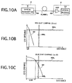
- the system shown in FIG. 10A is characterized in that an SMF is used as the optical fiber transmission line 6.
- an SMF is used as the optical fiber transmission line 6
- the zero-dispersion wavelength of the SMF is about 1.3 ⁇ m and the wavelength of the optical signal to be output from the optical transmitter 8 falls in a 1.55 ⁇ m band as mentioned previously, so that only a region of anomalous dispersion is given.
- the transmittable distance L9 becomes very short as shown in FIG. 10B.
- the transmittable distance L10 is longer than L9 by an amount produced in the case that the waveform or pulse width of the optical signal is compressed in the optical fiber line 6.
- the transmittable distance can be increased as shown by L10 by setting the chirp parameter ⁇ to a negative value so as to obtain a blue-shift chirping.
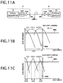
- the system shown in FIG. 11A is characterized in that an SMF is used as the optical fiber transmission line 6.
- dispersion compensating fibers (DCF) 126 and 128 are adopted to compensate for chromatic dispersion in the optical fiber transmission line 6, in view of the fact that the dispersion of an SMF in a 1.55 ⁇ m band is relatively large.
- the DCF 126 is optically connected between the optical transmitter 8 and the optical amplifier 124, and the DCF 128 is optically connected between the optical amplifier 122 and the optical receiver 12.
- An optical fiber having a dispersion (ps/nm/km) sufficiently larger than the dispersion of an SMF may be used as each of the DCFs 126 and 128, so as to suppress losses.
- the dispersion in each DCF falls in a region of normal dispersion, thereby performing dispersion compensation.
- the characteristic curve becomes three different characteristic curves as shown by (i), (ii), and (iii) in FIGS. 11B and 11C according to the dispersion induced by these DCFs.
- the optical signal to be output from the optical transmitter 8 has a red-shift chirping (0 ⁇ ⁇ ) as shown in FIG. 11B
- the three characteristic curves intersect each other on the upper side of the WDL. Accordingly, the transmittable distance L11 is given by the SNL.
- the optical signal to be output from the optical transmitter 8 has a blue-shift chirping ( ⁇ ⁇ 0) as shown in FIG. 11C
- the three characteristic curves intersect each other on the lower side of the WDL. Accordingly, the transmittable distance is given by three limited ranges as shown by L12.
- the transmittable distance can be increased or the range of the transmittable distance can be widened by setting the chirp parameter ⁇ to a positive value.
- FIG. 12 is a block diagram showing another preferred embodiment of the first terminal device 2 shown in FIG. 1.
- the optical transmitter 8 includes a modulator integrated laser diode (MI-LD) 212.
- the MI-LD 212 outputs an optical signal obtained by modulation according to a modulating signal MS from an FEC encoder 22.
- the optical signal is then supplied through an optical coupler 26 to the optical fiber transmission line 6 from its first end 6A.
- MI-LD modulator integrated laser diode
- control unit 10 controls or optimizes the operating conditions of the MI-LD 212, thereby adjusting the chirp parameter ⁇ of the optical signal to be output from the MI-LD 212 to an optimum value.
- the MI-LD 212 may be provided as a semiconductor chip having a directly coupled waveguide structure including a multiquantum well (MQW) layer of GaInAs, for example.
- the MI-LD 212 has an integrated structure consisting of a distributed feedback (DFB) laser diode (LD) 216 having a light emitting layer (active layer) 214 as a light source for generating CW light and of an electroabsorption optical modulator (EA modulator) 220 having an absorbing layer 218.
- DFB distributed feedback
- LD laser diode
- active layer active layer
- EA modulator electroabsorption optical modulator
- the active layer 214 and the absorbing layer 218 are monolithically directly coupled together.
- Reference numeral 222 denotes a common electrode for the LD 216 and the EA modulator 220.
- the LD 216 has an electrode 224 for receiving a bias current
- the EA modulator 220 has an electrode 226 for an applied voltage.
- the MI-LD 212 has the active layer 214 and the absorbing layer 218 monolithically directly coupled, the CW light generated from the active layer 214 is efficiently introduced into the absorbing layer 218. Accordingly, high output can be obtained from the optical transmitter 8. Further, because the MI-LD 212 is provided as a small semiconductor chip, the optical transmitter 8 can be reduced in size.
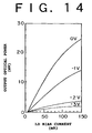
- FIG. 14 is a graph showing an example of the static characteristic of the MI-LD 212.
- the vertical axis represents output optical power (mW) from the EA modulator 212
- the horizontal axis represents bias current (mA) for the LD 216.
- the static characteristic shown is a relation between the output optical power and the bias current under the conditions where the electrode 222 is grounded and the potential at the electrode 226 is set to 0 V, -1 V, -2 V, and -3 V.
- an optical pulse having an extinction ratio of about 12 dB can be obtained as the optical signal by driving the EA modulator 212 with a pulse shape having a high level of 0 V and a low level of -3 V, for example.
- FIG. 15 is a graph showing a relation between attenuation (dB) and applied voltage (V) in the MI-LD 212. It is to be noted that the vertical axis in FIG. 15 corresponds to a common logarithm of output optical power from the MI-LD 212, because the attenuation is expressed in dB.
- the EA modulator 220 is driven by a reverse bias, and a negative voltage is therefore applied to the electrode 226.
- FIG. 15 shows an attenuation-applied voltage characteristic under the condition that the bias current for the LD 216 is 100 mA, and it is apparent from this characteristic that the attenuation increases with an increase in absolute value of the applied voltage to the EA modulator 220.
- FIG. 16 is a diagram showing an operating characteristic of the MI-LD 212.
- Reference numeral 228 denotes a characteristic curve showing a relation between output optical power (mW) and applied voltage (V) for the MI-LD 212. It is to be noted that the output optical power along the vertical axis in FIG. 16 is not expressed in dB and that the shape of the characteristic curve 228 is therefore different from the shape of the curve shown in FIG. 15.
- the characteristic curve 228 has a tendency that the optical output power decreases with an increase in absolute value of the applied voltage.
- the condition that the duty D is 100% means that the cross point between a rising line and a falling line in a digital signal coincides with the midpoint between the high level (H) and the low level (L) of the digital signal. Further, the condition that the duty D is smaller than 100% means that the cross point is shifted from the midpoint toward the low level, whereas the condition that the duty D is greater than 100% means that the cross point is shifted from the midpoint toward the high level.
- the duty D of the modulating signal MS is preferably set greater than 100% in advance as shown by reference numeral 236.
- FIG. 17 is a graph showing measured values of the chirp parameter ⁇ of the optical signal to be output from the MI-LD 212 with respect to various values of the applied voltage (V). It is understood from FIG. 17 that the chirp parameter ⁇ can be changed from a positive value to a negative value by changing the applied voltage.
- the chirp parameter ⁇ of the optical signal can be changed continuously.
- the control unit 10 includes an I/O port 238 for inputting and outputting signals which port includes an A/D converter and a D/A converter, a CPU 240 for computing target values of a bias voltage V B etc. according to a predetermined program, a ROM 242 preliminarily storing the program and data for a data table, a RAM 244 for temporarily storing a result of computation by the CPU 240, and a data bus 246 mutually connecting the I/O port 238, the CPU 240, the ROM 242, and the RAM 244.
- the receiving unit 18 includes a photodetector 82, a demodulating circuit 84, and a buffer 86.
- the supervisory information on the error count detected in the monitor unit 14 is transmitted from the transmitting unit 16 of the second terminal device 4 to the receiving unit 18 of the first terminal device 2, and then taken into the I/O port 238 directly from the buffer 86 of the receiving unit 18.
- control signal CS in this preferred embodiment is a signal to be transferred within the control unit 10.
- the MI-LD 212 is associated with a temperature controller 248. Data on the temperature of the MI-LD 212 is taken from the temperature controller 248 through the I/O port 238 into the CPU 240. A target value of the temperature of the MI-LD 212 is supplied from the CPU 240 through the I/O port 238 to the temperature controller 248.
- a bias current circuit 250 is provided to supply to the LD 216 a bias current I LD determining the amplitude of CW light generated in the LD 216.
- a target value of the bias current I LD is supplied from the CPU 240 through the I/O port 238 to the bias current circuit 250.
- a bias voltage circuit 252 for the EA modulator 220 generates a bias voltage V B , which is taken through the I/O port 238 into the CPU 240.
- the reason for inputting the bias voltage V B into the CPU 240 is to control the amplitude or the like of a modulating signal V MOD (obtained according to the modulating signal MS) to be superimposed on the bias voltage V B , according to the bias voltage V B .
- a target value of the bias voltage V B is supplied from the CPU 240 through the I/O port 238 to the bias voltage circuit 252. This target value is set so that the EA modulator 220 has an optimum value of the chirp parameter ⁇ .
- a drive circuit 253 is provided to superimpose the modulating signal V MOD on the bias voltage V B .
- the drive circuit 253 is associated with an amplitude varying circuit 254.
- a target value of the amplitude of the modulating signal V MOD is supplied from the CPU 240 through the I/O port 238 to the amplitude varying circuit 254.
- the amplitude varying circuit 254 controls the amplitude of the modulating signal V MOD to be output from the drive circuit 253 comes into coincidence with the target value.
- a duty varying circuit 256 is provided to control the duty of the modulating signal V MOD to be output from the drive circuit 253.
- a target value of the duty is supplied from the CPU 240 through the I/O port 238 to the duty varying circuit 256.
- a part of the optical signal output from the MI-LD 212 is extracted as monitor light by an optical coupler 26.
- the monitor light is then supplied to a photodetector 260.
- the photodetector 260 outputs an electrical signal having a level corresponding to the power of the optical signal to be output from the optical transmitter 8. This electrical signal is taken through the I/O port 238 into the CPU 240.
- FIG. 18A corresponds to the case that a bias voltage V B- having a relatively large absolute value is set to obtain a negative chirp parameter ⁇ .
- the bias voltage V B- corresponds to the cross point in the waveform of the optical signal.
- the characteristic curve shown in each of FIGS. 18A and 18B corresponds to the characteristic curve 228 shown in FIG. 16.
- the amplitude of the modulating signal V MOD is preferably increased with an increase in the absolute value of the bias voltage.
- the extinction ratio of the optical signal is 1:3 for the amplitude V1 of the modulating signal V MOD .
- the duty of the modulating signal V MOD is set to D1 (> 100%) so that the cross point in the waveform of the optical signal coincides with the midpoint between the high level and the low level.
- Optimum values of the amplitude and duty of the modulating signal V MOD are determined in one-to-one corresponding relationship with the bias voltage for a given characteristic curve. Accordingly, optimum values of the amplitude and duty of the modulating signal V MOD corresponding to various values of the bias voltage are preliminarily stored as a table in the ROM 242 shown in FIG. 12, and the CPU 240 computes target values of the amplitude and duty of the modulating signal V MOD according to the stored table.
- the amplitude of the modulating signal V MOD is changed to V2 ( ⁇ V1), so as to maintain the extinction ratio constant. Further, the duty of the modulating signal V MOD is changed to D2 (> D1) so that the cross point in the waveform of the optical signal coincides with the midpoint between the high level and the low level.
- the output power of the optical signal decreases with an increase in the absolute value of the bias voltage in the case that the power of the CW light is constant.
- a target value of the bias current to be supplied from the bias current circuit 250 to the LD 216 is set so that the power of the CW light increases with an increase in the absolute value of the bias voltage.
- feedforward control may be adopted.
- Optimum values of the bias current for the LD 216 corresponding to various values of the bias voltage are determined for a given characteristic curve. Accordingly, the optimum values of the bias current are preliminarily stored in the ROM 242, and a target value of the bias current for the LD 216 is calculated by the CPU 240 according to a value of the bias voltage taken from the bias voltage circuit 252.
- feedback control for the bias current for the LD 216 may be performed because the photodetector 260 for receiving a part of the optical signal output from the MI-LD 212 is provided in the preferred embodiment shown in FIG. 12. That is, the CPU 240 sequentially calculates a target value of the bias current so that the output signal level of the photodetector 260 becomes constant, and the bias current circuit 250 supplies the calculated target value of the bias current to the LD 216.
- the absolute value of the bias voltage to be supplied to the EA modulator 220 is increased for the merit of obtaining a blue-shift chirping, for example, there arises a demerit that the extinction ratio of the output optical signal is degraded and the optical output power is reduced. Accordingly, it is preferable to determine the driving conditions for the EA modulator 220 according to losses and chromatic dispersion in the optical fiber transmission line 6 in consideration of the above-mentioned merit versus demerit trade-off.
- the driving parameters to be controlled include the temperature of the EA modulator 220 itself or the temperature of the MI-LD 212 in addition to the bias voltage for the EA modulator 220, the duty and amplitude of the modulating signal for the EA modulator 220, and the bias current for the LD 216 as mentioned above.
- the optical transmitter 8 includes the MI-LD 212, so that the efficiency of coupling between the light source and the modulator can be improved, and a high-output and compact optical transmitter can be provided. Further, temperature control for the light source and the modulator can be performed by the single temperature controller 248.
- the chirp parameter ⁇ of the optical signal to be output from the optical transmitter 8 can be adjusted to an optimum value so that the bit error to be detected in the second terminal device 4 is minimized, in accordance with the specific operation of the control unit 10, thus suppressing the influence of a waveform degradation due to chromatic dispersion and nonlinearity.
- the program for the operation of the control unit 10 may be modified in such a manner that the bias voltage circuit 252 selectively generates a first bias voltage for providing a positive first chirp parameter and a second bias voltage for providing a negative second chirp parameter.
- the bias voltage circuit 252 selectively generates a first bias voltage for providing a positive first chirp parameter and a second bias voltage for providing a negative second chirp parameter.
- values of -0.4 V and -1.7 V are given as the first and second bias voltages, respectively, so as to switch the chirp parameter between +1 and -1 respectively shown by points A and B.
- computation in the CPU 240 can be simplified as compared with the case that the CPU 240 calculates a target value of the bias voltage corresponding to an optimum value of the chirp parameter.
- At least one optical repeater including an optical amplifier may be arranged along the optical fiber transmission line 6.
- the terminal device can control a chirp parameter according to supervisory information on a bit error detected in relation to an optical signal transmitted by an optical fiber transmission line, so that versatility to a change in transmission route or the like can be increased.
Landscapes
- Physics & Mathematics (AREA)
- Nonlinear Science (AREA)
- Electromagnetism (AREA)
- Engineering & Computer Science (AREA)
- Computer Networks & Wireless Communication (AREA)
- Signal Processing (AREA)
- General Physics & Mathematics (AREA)
- Optics & Photonics (AREA)
- Optical Communication System (AREA)
Applications Claiming Priority (2)
| Application Number | Priority Date | Filing Date | Title |
|---|---|---|---|
| JP6838598 | 1998-03-18 | ||
| JP10068385A JPH11266200A (ja) | 1998-03-18 | 1998-03-18 | 光ファイバ通信のための方法並びに該方法の実施に使用される装置及びシステム |
Publications (1)
| Publication Number | Publication Date |
|---|---|
| EP0944191A1 true EP0944191A1 (en) | 1999-09-22 |
Family
ID=13372217
Family Applications (1)
| Application Number | Title | Priority Date | Filing Date |
|---|---|---|---|
| EP99102790A Ceased EP0944191A1 (en) | 1998-03-18 | 1999-02-24 | Method for optical fiber communication, and device and system for use in carrying out the method |
Country Status (4)
| Country | Link |
|---|---|
| US (1) | US7006769B1 (ja) |
| EP (1) | EP0944191A1 (ja) |
| JP (1) | JPH11266200A (ja) |
| CN (1) | CN1222123C (ja) |
Cited By (8)
| Publication number | Priority date | Publication date | Assignee | Title |
|---|---|---|---|---|
| WO2001067165A2 (en) * | 2000-03-09 | 2001-09-13 | Optium, Inc. | Apparatuses and methods for generating optical signals |
| EP1209828A2 (en) * | 2000-11-28 | 2002-05-29 | Nec Corporation | Optical transmission system and optical transmission method |
| EP1223694A2 (en) * | 2001-01-10 | 2002-07-17 | Fujitsu Limited | Dispersion compensating method, dispersion compensating apparatus and optical transmission system |
| WO2002078219A1 (en) * | 2001-03-23 | 2002-10-03 | Axe, Inc. | Intelligent performance monitoring in optical networks using fec statistics |
| EP1271809A2 (en) * | 2001-06-29 | 2003-01-02 | KDDI Submarine Cable Systems Inc. | Optical reception apparatus and optical transmission system |
| US7302188B2 (en) | 2002-01-30 | 2007-11-27 | Mitsubishi Denki Kabushiki Kaisha | Disperse equalizer and disperse equalizing method |
| US7742702B2 (en) | 2005-10-18 | 2010-06-22 | Fujitsu Limited | Chirp switching circuit and optical transmission system |
| WO2016170746A1 (en) * | 2015-04-20 | 2016-10-27 | Sony Corporation | Communication device, communication system, and communication method |
Families Citing this family (25)
| Publication number | Priority date | Publication date | Assignee | Title |
|---|---|---|---|---|
| JP4495326B2 (ja) * | 2000-09-29 | 2010-07-07 | 住友大阪セメント株式会社 | 光変調素子のチャープ制御方法 |
| JP4741118B2 (ja) * | 2001-08-20 | 2011-08-03 | 株式会社日立製作所 | 光伝送システム、波長多重器、および、波長多重伝送システムの分散補償方法 |
| JP4569064B2 (ja) * | 2001-09-27 | 2010-10-27 | 住友電気工業株式会社 | 光送信機及び波長分割多重伝送システム |
| US7308210B2 (en) * | 2002-04-05 | 2007-12-11 | Kabushiki Kaisha Toshiba | Optical modulating device, optical transmitting apparatus using the same, method of controlling optical modulating device, and control program recording medium |
| US7403718B2 (en) * | 2002-04-24 | 2008-07-22 | Lucent Technologies Inc. | Modulation phase shift to compensate for optical passband shift |
| JP3990228B2 (ja) | 2002-08-15 | 2007-10-10 | 富士通株式会社 | 光送信装置 |
| CN100407601C (zh) * | 2003-03-16 | 2008-07-30 | 华为技术有限公司 | 一种模拟光信号误码的装置和方法 |
| CN100428659C (zh) * | 2003-08-30 | 2008-10-22 | 华为技术有限公司 | 单板老化环节的测试方法 |
| JP4366225B2 (ja) * | 2004-03-26 | 2009-11-18 | 富士通株式会社 | 分散補償方法及びその装置 |
| JP2006054660A (ja) * | 2004-08-11 | 2006-02-23 | Nippon Telegr & Teleph Corp <Ntt> | 光送信装置および光伝送システム |
| JP2007068077A (ja) * | 2005-09-02 | 2007-03-15 | Nippon Telegr & Teleph Corp <Ntt> | 高速光伝送システム及び高速光伝送方法 |
| JP5211528B2 (ja) * | 2007-03-29 | 2013-06-12 | 富士通株式会社 | 光変調装置および光変調方式切替方法 |
| JP2010011098A (ja) * | 2008-06-27 | 2010-01-14 | Fujitsu Ltd | 光伝送装置 |
| JP5907175B2 (ja) * | 2011-12-07 | 2016-04-26 | 日本電気株式会社 | 光通信装置、光送信器および光送信方法 |
| CN102866647B (zh) * | 2012-09-21 | 2014-12-17 | 深圳市英威腾电气股份有限公司 | 信号控制方法与信号传输方法、相关设备及系统 |
| JP5761235B2 (ja) * | 2013-03-06 | 2015-08-12 | 横河電機株式会社 | 光ファイバ温度分布測定装置 |
| CN105052056B (zh) * | 2013-03-15 | 2018-05-22 | 日本电气株式会社 | 光发射/接收设备、光通信系统、以及光发射/接收方法 |
| US9369210B2 (en) * | 2014-05-21 | 2016-06-14 | Fujitsu Limited | Optical modulator calibration |
| JP2016059024A (ja) * | 2014-09-11 | 2016-04-21 | 富士通株式会社 | 光通信装置および光通信システム |
| JP6554897B2 (ja) * | 2015-04-22 | 2019-08-07 | ソニー株式会社 | 通信装置および通信システム |
| CN107534488B (zh) * | 2015-04-27 | 2021-03-12 | 三菱电机株式会社 | 虚拟光生成装置、光传输装置及虚拟光生成方法 |
| CN110892650B (zh) * | 2017-07-14 | 2022-12-09 | 日本电气株式会社 | 可插拔光学模块、光学通信系统以及可插拔光学模块的控制方法 |
| KR102041275B1 (ko) * | 2018-03-02 | 2019-11-06 | 한국광기술원 | 광통신 시스템 |
| EP3832910A1 (en) * | 2019-12-06 | 2021-06-09 | ID Quantique S.A. | Quantum bit error rate minimization method |
| CN113014323B (zh) | 2019-12-20 | 2024-02-09 | 光联通讯技术有限公司美国分部 | 光传送装置及光通信系统 |
Citations (5)
| Publication number | Priority date | Publication date | Assignee | Title |
|---|---|---|---|---|
| US5524076A (en) * | 1994-01-28 | 1996-06-04 | Northern Telecom Limited | Chirp control of a Mach-Zehnder optical modulator using non-equal power splitting |
| WO1996023372A1 (en) * | 1995-01-27 | 1996-08-01 | Pirelli Cavi S.P.A. | Dispersion compensation in optical fibre transmission |
| GB2308675A (en) * | 1995-12-26 | 1997-07-02 | Fujitsu Ltd | Driving an optical modulator |
| EP0812075A2 (en) * | 1996-06-07 | 1997-12-10 | Nortel Networks Corporation | Optical fibre transmission systems including dispersion measurement and compensation |
| GB2316821A (en) * | 1996-09-03 | 1998-03-04 | Fujitsu Ltd | Optical modulator using time division multiplexing and chirping |
Family Cites Families (16)
| Publication number | Priority date | Publication date | Assignee | Title |
|---|---|---|---|---|
| JPS61212125A (ja) | 1985-03-15 | 1986-09-20 | Nec Corp | 光パルス送信方法および装置 |
| JPH02288640A (ja) * | 1989-04-28 | 1990-11-28 | Nec Corp | 光受信回路 |
| JPH03171036A (ja) | 1989-11-30 | 1991-07-24 | Nec Corp | 光ファイバ通信方法およびシステム |
| JP2848942B2 (ja) * | 1990-10-02 | 1999-01-20 | 富士通株式会社 | 光送信装置 |
| JP3036876B2 (ja) * | 1991-03-20 | 2000-04-24 | 日本電気株式会社 | 光送信装置 |
| JPH05110516A (ja) | 1991-10-21 | 1993-04-30 | Nec Corp | 光中継伝送方式および光中継回路 |
| JPH07154378A (ja) * | 1993-12-01 | 1995-06-16 | Kokusai Denshin Denwa Co Ltd <Kdd> | 光伝送特性測定装置 |
| JP3846918B2 (ja) * | 1994-08-02 | 2006-11-15 | 富士通株式会社 | 光伝送システム、光多重伝送システム及びその周辺技術 |
| JPH0886988A (ja) * | 1994-09-17 | 1996-04-02 | Toshiba Corp | 光半導体素子 |
| US5784184A (en) * | 1995-05-11 | 1998-07-21 | Ciena Corporation | WDM Optical communication systems with remodulators and remodulating channel selectors |
| JPH09152564A (ja) * | 1995-11-30 | 1997-06-10 | Oki Electric Ind Co Ltd | 光送信装置 |
| JP3522044B2 (ja) | 1996-04-19 | 2004-04-26 | 富士通株式会社 | 光伝送システム |
| US6252692B1 (en) * | 1996-06-07 | 2001-06-26 | Nortel Networks Limited | Optical fibre transmission systems |
| JPH1096879A (ja) * | 1996-09-20 | 1998-04-14 | Nec Corp | 半導体光変調器とこれを用いた光通信装置 |
| JPH10163971A (ja) * | 1996-11-25 | 1998-06-19 | Fujitsu Ltd | 光信号の波長を制御するための方法、装置及びシステム |
| US6115403A (en) * | 1997-07-22 | 2000-09-05 | Ciena Corporation | Directly modulated semiconductor laser having reduced chirp |
-
1998
- 1998-03-18 JP JP10068385A patent/JPH11266200A/ja active Pending
-
1999
- 1999-02-24 US US09/256,079 patent/US7006769B1/en not_active Expired - Fee Related
- 1999-02-24 EP EP99102790A patent/EP0944191A1/en not_active Ceased
- 1999-03-18 CN CNB991041240A patent/CN1222123C/zh not_active Expired - Fee Related
Patent Citations (5)
| Publication number | Priority date | Publication date | Assignee | Title |
|---|---|---|---|---|
| US5524076A (en) * | 1994-01-28 | 1996-06-04 | Northern Telecom Limited | Chirp control of a Mach-Zehnder optical modulator using non-equal power splitting |
| WO1996023372A1 (en) * | 1995-01-27 | 1996-08-01 | Pirelli Cavi S.P.A. | Dispersion compensation in optical fibre transmission |
| GB2308675A (en) * | 1995-12-26 | 1997-07-02 | Fujitsu Ltd | Driving an optical modulator |
| EP0812075A2 (en) * | 1996-06-07 | 1997-12-10 | Nortel Networks Corporation | Optical fibre transmission systems including dispersion measurement and compensation |
| GB2316821A (en) * | 1996-09-03 | 1998-03-04 | Fujitsu Ltd | Optical modulator using time division multiplexing and chirping |
Cited By (15)
| Publication number | Priority date | Publication date | Assignee | Title |
|---|---|---|---|---|
| WO2001067165A3 (en) * | 2000-03-09 | 2002-03-14 | Optium Inc | Apparatuses and methods for generating optical signals |
| WO2001067165A2 (en) * | 2000-03-09 | 2001-09-13 | Optium, Inc. | Apparatuses and methods for generating optical signals |
| EP1209828A3 (en) * | 2000-11-28 | 2003-08-20 | Nec Corporation | Optical transmission system and optical transmission method |
| EP1209828A2 (en) * | 2000-11-28 | 2002-05-29 | Nec Corporation | Optical transmission system and optical transmission method |
| EP1223694A2 (en) * | 2001-01-10 | 2002-07-17 | Fujitsu Limited | Dispersion compensating method, dispersion compensating apparatus and optical transmission system |
| EP1223694A3 (en) * | 2001-01-10 | 2004-06-16 | Fujitsu Limited | Dispersion compensating method, dispersion compensating apparatus and optical transmission system |
| US6871024B2 (en) | 2001-01-10 | 2005-03-22 | Fujitsu Limited | Dispersion compensating method, dispersion compensating apparatus and optical transmission system |
| EP1928108A1 (en) * | 2001-01-10 | 2008-06-04 | Fujitsu Limited | Dispersion compensating method, dispersion compensating apparatus and optical transmission system |
| WO2002078219A1 (en) * | 2001-03-23 | 2002-10-03 | Axe, Inc. | Intelligent performance monitoring in optical networks using fec statistics |
| EP1271809A2 (en) * | 2001-06-29 | 2003-01-02 | KDDI Submarine Cable Systems Inc. | Optical reception apparatus and optical transmission system |
| EP1271809A3 (en) * | 2001-06-29 | 2004-12-08 | KDDI Submarine Cable Systems Inc. | Optical reception apparatus and optical transmission system |
| US7302188B2 (en) | 2002-01-30 | 2007-11-27 | Mitsubishi Denki Kabushiki Kaisha | Disperse equalizer and disperse equalizing method |
| US7742702B2 (en) | 2005-10-18 | 2010-06-22 | Fujitsu Limited | Chirp switching circuit and optical transmission system |
| WO2016170746A1 (en) * | 2015-04-20 | 2016-10-27 | Sony Corporation | Communication device, communication system, and communication method |
| US10389436B2 (en) | 2015-04-20 | 2019-08-20 | Sony Corporation | Communication device, communication system, and communication method |
Also Published As
| Publication number | Publication date |
|---|---|
| JPH11266200A (ja) | 1999-09-28 |
| CN1230827A (zh) | 1999-10-06 |
| US7006769B1 (en) | 2006-02-28 |
| CN1222123C (zh) | 2005-10-05 |
Similar Documents
| Publication | Publication Date | Title |
|---|---|---|
| US7006769B1 (en) | Method for optical fiber communication, and device and system for use in carrying out the method | |
| EP1079552B1 (en) | Method, optical device, and system for optical fiber transmission | |
| JP3583846B2 (ja) | 光変調器の駆動方法及び装置並びに光通信システム | |
| US6583910B1 (en) | Optical transmitter and optical communication system using the same | |
| US6738584B1 (en) | Method for optical fiber communication, and terminal device and system for use in carrying out the method | |
| US6608854B1 (en) | Method, device, and system for waveform shaping of signal light | |
| US7321736B2 (en) | Optical receiving station, optical communication system, and dispersion controlling method | |
| US7639955B2 (en) | Method and apparatus for transmitting a signal using a chirp managed laser (CML) and an optical spectrum reshaper (OSR) before an optical receiver | |
| US6191854B1 (en) | Optical telecommunications system | |
| US6091535A (en) | Optical transmitter and optical transmission system with switchable chirp polarity | |
| US5973812A (en) | Optical transmitter and optical communication system | |
| JPH08316909A (ja) | 光伝送システム、光送信モジュール、及び光変調器の駆動方法 | |
| JP2002023208A (ja) | 信号光を波形整形するための方法及び装置 | |
| US7103285B1 (en) | Optical transmission system for reducing nonlinear optical phenomena using modulation depth control system | |
| JP2839105B2 (ja) | 長距離用高速光通信方式 | |
| EP1271810B1 (en) | Method and device for shaping the waveform of an optical signal | |
| CA2310305C (en) | Distortion compensation in optically amplified lightwave communication systems | |
| JPH09275375A (ja) | 光通信装置 | |
| MXPA02002476A (es) | Senales con chirrido positivo en sistemas opticos de comunicacion. | |
| JP2000036794A (ja) | 光伝送装置 | |
| KR100198948B1 (ko) | 신호대 잡음비가 개선된 광전송장치 | |
| JP2004185021A (ja) | 信号光の波形整形のための方法、装置及びシステム | |
| Bryant et al. | Field Demonstration of FSK Transmission at 2.488 Gbit/s Over a 132km Submarine Cable Using an Erbium Power Amplifier | |
| JPH09139715A (ja) | 光送信機 | |
| Bryant et al. | A 2.488 Gbit/s FSK field demonstration over a 132 km submarine cable employing an erbium power amplifier |
Legal Events
| Date | Code | Title | Description |
|---|---|---|---|
| PUAI | Public reference made under article 153(3) epc to a published international application that has entered the european phase |
Free format text: ORIGINAL CODE: 0009012 |
|
| AK | Designated contracting states |
Kind code of ref document: A1 Designated state(s): DE FR GB |
|
| AX | Request for extension of the european patent |
Free format text: AL;LT;LV;MK;RO;SI |
|
| 17P | Request for examination filed |
Effective date: 20000105 |
|
| AKX | Designation fees paid |
Free format text: DE FR GB |
|
| 17Q | First examination report despatched |
Effective date: 20031128 |
|
| APBN | Date of receipt of notice of appeal recorded |
Free format text: ORIGINAL CODE: EPIDOSNNOA2E |
|
| APBR | Date of receipt of statement of grounds of appeal recorded |
Free format text: ORIGINAL CODE: EPIDOSNNOA3E |
|
| APAF | Appeal reference modified |
Free format text: ORIGINAL CODE: EPIDOSCREFNE |
|
| APBT | Appeal procedure closed |
Free format text: ORIGINAL CODE: EPIDOSNNOA9E |
|
| STAA | Information on the status of an ep patent application or granted ep patent |
Free format text: STATUS: THE APPLICATION HAS BEEN REFUSED |
|
| 18R | Application refused |
Effective date: 20071120 |