EP0944094B1 - Power switching circuit - Google Patents
Power switching circuit Download PDFInfo
- Publication number
- EP0944094B1 EP0944094B1 EP99110956A EP99110956A EP0944094B1 EP 0944094 B1 EP0944094 B1 EP 0944094B1 EP 99110956 A EP99110956 A EP 99110956A EP 99110956 A EP99110956 A EP 99110956A EP 0944094 B1 EP0944094 B1 EP 0944094B1
- Authority
- EP
- European Patent Office
- Prior art keywords
- voltage
- transistor
- power line
- source
- gate
- Prior art date
- Legal status (The legal status is an assumption and is not a legal conclusion. Google has not performed a legal analysis and makes no representation as to the accuracy of the status listed.)
- Expired - Lifetime
Links
Images


Classifications
-
- G—PHYSICS
- G11—INFORMATION STORAGE
- G11C—STATIC STORES
- G11C16/00—Erasable programmable read-only memories
- G11C16/02—Erasable programmable read-only memories electrically programmable
- G11C16/06—Auxiliary circuits, e.g. for writing into memory
-
- G—PHYSICS
- G11—INFORMATION STORAGE
- G11C—STATIC STORES
- G11C29/00—Checking stores for correct operation ; Subsequent repair; Testing stores during standby or offline operation
- G11C29/70—Masking faults in memories by using spares or by reconfiguring
- G11C29/78—Masking faults in memories by using spares or by reconfiguring using programmable devices
- G11C29/80—Masking faults in memories by using spares or by reconfiguring using programmable devices with improved layout
- G11C29/816—Masking faults in memories by using spares or by reconfiguring using programmable devices with improved layout for an application-specific layout
- G11C29/82—Masking faults in memories by using spares or by reconfiguring using programmable devices with improved layout for an application-specific layout for EEPROMs
-
- G—PHYSICS
- G05—CONTROLLING; REGULATING
- G05F—SYSTEMS FOR REGULATING ELECTRIC OR MAGNETIC VARIABLES
- G05F3/00—Non-retroactive systems for regulating electric variables by using an uncontrolled element, or an uncontrolled combination of elements, such element or such combination having self-regulating properties
- G05F3/02—Regulating voltage or current
- G05F3/08—Regulating voltage or current wherein the variable is DC
- G05F3/10—Regulating voltage or current wherein the variable is DC using uncontrolled devices with non-linear characteristics
- G05F3/16—Regulating voltage or current wherein the variable is DC using uncontrolled devices with non-linear characteristics being semiconductor devices
- G05F3/20—Regulating voltage or current wherein the variable is DC using uncontrolled devices with non-linear characteristics being semiconductor devices using diode- transistor combinations
- G05F3/205—Substrate bias-voltage generators
-
- G—PHYSICS
- G11—INFORMATION STORAGE
- G11C—STATIC STORES
- G11C16/00—Erasable programmable read-only memories
- G11C16/02—Erasable programmable read-only memories electrically programmable
- G11C16/04—Erasable programmable read-only memories electrically programmable using variable threshold transistors, e.g. FAMOS
- G11C16/0408—Erasable programmable read-only memories electrically programmable using variable threshold transistors, e.g. FAMOS comprising cells containing floating gate transistors
- G11C16/0416—Erasable programmable read-only memories electrically programmable using variable threshold transistors, e.g. FAMOS comprising cells containing floating gate transistors comprising cells containing a single floating gate transistor and no select transistor, e.g. UV EPROM
-
- G—PHYSICS
- G11—INFORMATION STORAGE
- G11C—STATIC STORES
- G11C16/00—Erasable programmable read-only memories
- G11C16/02—Erasable programmable read-only memories electrically programmable
- G11C16/06—Auxiliary circuits, e.g. for writing into memory
- G11C16/08—Address circuits; Decoders; Word-line control circuits
-
- G—PHYSICS
- G11—INFORMATION STORAGE
- G11C—STATIC STORES
- G11C16/00—Erasable programmable read-only memories
- G11C16/02—Erasable programmable read-only memories electrically programmable
- G11C16/06—Auxiliary circuits, e.g. for writing into memory
- G11C16/10—Programming or data input circuits
- G11C16/14—Circuits for erasing electrically, e.g. erase voltage switching circuits
- G11C16/16—Circuits for erasing electrically, e.g. erase voltage switching circuits for erasing blocks, e.g. arrays, words, groups
-
- G—PHYSICS
- G11—INFORMATION STORAGE
- G11C—STATIC STORES
- G11C16/00—Erasable programmable read-only memories
- G11C16/02—Erasable programmable read-only memories electrically programmable
- G11C16/06—Auxiliary circuits, e.g. for writing into memory
- G11C16/30—Power supply circuits
-
- G—PHYSICS
- G11—INFORMATION STORAGE
- G11C—STATIC STORES
- G11C5/00—Details of stores covered by group G11C11/00
- G11C5/14—Power supply arrangements, e.g. power down, chip selection or deselection, layout of wirings or power grids, or multiple supply levels
- G11C5/145—Applications of charge pumps; Boosted voltage circuits; Clamp circuits therefor
-
- H—ELECTRICITY
- H03—ELECTRONIC CIRCUITRY
- H03K—PULSE TECHNIQUE
- H03K19/00—Logic circuits, i.e. having at least two inputs acting on one output; Inverting circuits
- H03K19/0175—Coupling arrangements; Interface arrangements
- H03K19/0185—Coupling arrangements; Interface arrangements using field effect transistors only
- H03K19/018507—Interface arrangements
- H03K19/018521—Interface arrangements of complementary type, e.g. CMOS
-
- H—ELECTRICITY
- H03—ELECTRONIC CIRCUITRY
- H03K—PULSE TECHNIQUE
- H03K19/00—Logic circuits, i.e. having at least two inputs acting on one output; Inverting circuits
- H03K19/20—Logic circuits, i.e. having at least two inputs acting on one output; Inverting circuits characterised by logic function, e.g. AND, OR, NOR, NOT circuits
- H03K19/21—EXCLUSIVE-OR circuits, i.e. giving output if input signal exists at only one input; COINCIDENCE circuits, i.e. giving output only if all input signals are identical
- H03K19/215—EXCLUSIVE-OR circuits, i.e. giving output if input signal exists at only one input; COINCIDENCE circuits, i.e. giving output only if all input signals are identical using field-effect transistors
-
- H—ELECTRICITY
- H03—ELECTRONIC CIRCUITRY
- H03K—PULSE TECHNIQUE
- H03K3/00—Circuits for generating electric pulses; Monostable, bistable or multistable circuits
- H03K3/02—Generators characterised by the type of circuit or by the means used for producing pulses
- H03K3/353—Generators characterised by the type of circuit or by the means used for producing pulses by the use, as active elements, of field-effect transistors with internal or external positive feedback
- H03K3/356—Bistable circuits
- H03K3/356104—Bistable circuits using complementary field-effect transistors
- H03K3/356113—Bistable circuits using complementary field-effect transistors using additional transistors in the input circuit
- H03K3/356147—Bistable circuits using complementary field-effect transistors using additional transistors in the input circuit using pass gates
-
- H—ELECTRICITY
- H03—ELECTRONIC CIRCUITRY
- H03K—PULSE TECHNIQUE
- H03K3/00—Circuits for generating electric pulses; Monostable, bistable or multistable circuits
- H03K3/02—Generators characterised by the type of circuit or by the means used for producing pulses
- H03K3/353—Generators characterised by the type of circuit or by the means used for producing pulses by the use, as active elements, of field-effect transistors with internal or external positive feedback
- H03K3/356—Bistable circuits
- H03K3/356104—Bistable circuits using complementary field-effect transistors
- H03K3/356165—Bistable circuits using complementary field-effect transistors using additional transistors in the feedback circuit
Definitions
- the present invention relates to a so-called flash memory or a nonvolatile semiconductor memory from which existent information can be electrically erased concurrently or block by block.
- this invention is concerned with improvements in erasing a flash memory and improvements in the associated circuitry.
- the semiconductor memories are nonvolatile memories which are made rewritable by electrically erasing specified data previously written therein.
- CMOS complementary metal-oxide-semiconductor
- EEPROM erasable programmable read only memory
- the EPROM has the advantage of a small cell size.
- data erasing is a nuisance because ultraviolet light must be used to erase data.
- data erasing is easy to do because data can be erased electrically.
- the cell size in the EEPROM is larger than that in the EPROM, which makes it difficult to increase the capacity of an EEPROM.
- flash memory flash memory
- the nonvolatile semiconductor memory has an overall configuration, for example, as that shown in Fig. 1.
- N cell blocks 11 1 to 11 N (for example, eight blocks) each having multiple transistor cells are arranged in a row.
- the cell blocks 11 1 to 11 N are provided with bit line select circuits 12 1 to 12 N and sense amplifiers/sense buffers 13 1 to 13 N respectively.
- a row address signal is supplied from a row address buffer to each of the cell blocks 11 1 to 11 N via a row decoder 15.
- a column address signal is supplied from a column address buffer 16 to each of the bit line select circuits 12 1 to 12 N via a column address decoder 17.
- a voltage V S sent from a source power supply circuit 18 is applied to each of source electrodes of the transistor cells of the cell blocks 11 1 to 11 N .
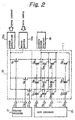
- Fig. 2 shows the cell block 11, one of the cells blocks in the aforesaid nonvolatile semiconductor memory, and its peripheral circuitry.
- the bit line select circuit 12 comprises n-channel MOS field-effect transistors Q1 to Qn. Column address signals Y1 to Yn are fed from the column decoder 17 to the gates of the transistors Q1 to Qn.
- the cell block 11 comprises a total of n by n field-effect transistors Q11 to Qnn having floating gates and control gates.
- the drains of the n transistors Qli to Qni arranged in tandem are connected to the drains of the transistors Qi in the bit line select circuit 12 via bit lines. Voltage from the source power circuit 18 is applied to each of the sources of the transistors Qll to Qnn.
- a cell amplifier 13a and a write buffer 13b are connected to each of the sources of the transistors Q1 to Qn.
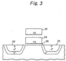
- Fig. 3 shows an example of a structure of a memory cell.
- a gate has a two-layered structure consisting of a control gate (CG) 25 and a floating gate (FG) 24.
- the control gate 25 is connected to a word line WLi and a drain (D) 23 is connected to a bit line BLi.
- Reference numeral 26 denotes a tunneling oxide film.
- the flash memory is broadly divided into two types of what are referred to as NOR and NAND. These types differ from each other in a method of writing, reading, or erasing information into or from a memory cell. Taking the NOR type flash memory as an example, writing, reading, or erasing information into or from a memory cell will be described below.
- the word line WLi is set to Vpp (approx. 12 V)
- the bit line BLi is set to approx. 6 V
- the source S is set to 0 V.
- High voltage is then applied to the control gate CG and drain D. Current then flows into the memory cell. Part of the electrons flowing through the memory cell are accelerated due to the high electric field in the vicinity of the drain D, gain energy, and then goes beyond the energy barrier of an insulating film of the floating gate. The electrons are finally injected into the floating gate FG.
- the floating gate FG is not electrically coupled with other circuits, so it therefore can retain charges on a semi-permanent basis.
- the word line WLi is set to Vcc (about 5 V)
- the bit line BLi is set to about 1 V
- the source S is set to 0 V.
- the memory cell is then selected by specifying the word line WLi and bit line BLi.
- the threshold value of the cell transistor varies depending on the charges retained in the floating gate FG. Current flowing through the selected memory cell varies depending on the information stored therein. The information therefore can be read out by detecting and amplifying the current.
- the voltage levels of the control gate CG, drain D, source S, and substrate PS in the aforesaid operative states are set to the values listed in Table 1. Voltages in modes in a prior art CG D S PS Reading Vcc to 1 V 0 V 0 V Writing Vpp to 6 V 0 V 0 V Erasing 0 V Float Vpp 0 V
- the word line WLi is set to about 0 V and the bit line BLi is opened.
- the drain D is opened, about 0 volt is applied to the control gate CG, and a high voltage of about 12 volts is applied to the source S.
- Vss line in the source For divided erasing, it is required that the Vss line in the source must partly have a different voltage. This leads to disconnection or an increased number of drive circuits. Eventually, chip size increases.
- a solution to the above problem is to apply a negative voltage to the word line WLi.
- a negative voltage (about - 10 V) is applied to the control gate CG and Vcc (about 5 V) is applied to the source S.
- the drain D is opened. Erasing is then executed.
- Partial erasing is enabled by selectively applying negative voltage to the control gates CG.
- the aforesaid erasing method is a source erasing method in which charges in the floating gate FG are routed to the source.
- a channel erasing method is also available, wherein charges in the floating gate are routed to a channel; that is, a substrate. Even in this method, negative voltage is applied to the control gate.
- the channel erasing method is sometimes employed for the aforesaid NAND-type flash memory.
- Figs. 8 to 11 show the states of a memory cell with voltage applied according to various erasing methods.
- the memory cell is an n-channel transistor.
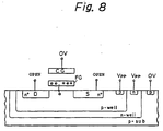
- Fig. 8 shows a state in which positive voltage is applied according to a channel erasing method.
- the drain D and source S are opened, and the control gate CG is set to 0 V.
- the high voltage Vpp is applied to the P well equivalent to a channel.
- a triple-well structure shown in Fig. 8 is adopted because positive bias is applied to the channel.
- Fig. 9 shows a state in which a positive voltage is applied according to the source erasing method.
- the drain D is opened, and then the control gate CG is set to 0 V.
- the high voltage Vpp is applied to the source S.
- the substrate is opened or set to 0 V.
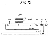
- Fig. 10 shows a state in which a negative voltage is applied according to the channel erasing method.
- the drain D and source S are opened, and the control gate CG is set to a negative voltage V BB .
- a positive voltage Vcc is applied to the p well equivalent to a channel.
- V BB - Vcc is applied between the control gate CG and channel.
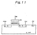
- Fig. 11 shows a state in which negative voltage is applied according to the source erasing method.
- the drain D is opened, and then the control gate CG is set to the negative voltage V BB .
- the source S is set to the positive voltage Vcc.
- a flash memory includes an internal power switching circuit for switching supply voltages depending on a mode.
- a previously-proposed internal power switching circuit has a simple circuitry but is likely to cause a latch-up phenomenon. The switching speed is decreased in order to avoid the latch-up phenomenon. This contradicts efforts to speeding up processing.
- an internal power switching circuit for use in a flash memory or the like, comprising a first MOS transistor of a first polarity one of whose drain and source electrodes is connected to a first power line and the other of whose drain and source electrodes is connected to a second power line;
- the fourth MOS transistor assists in boosting the voltage of the second power line. This helps minimize the channel current in the second MOS transistor. A latch-up phenomenon can therefore be avoided.
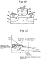
- Fig. 12 shows a structure of a memory cell shown in Fig. 3 in more detail.
- a transistor serving as the memory cell has, as shown in Fig. 12, such a structure that n-type diffusive regions 32 and 33 are formed in a p-type substrate 31 with a certain space between them.
- a floating gate (FG) 34 and a control gate (CG) 35 are formed above the p-type substrate 31, and coated with an oxide film 36.
- the n-type diffusive regions 32 and 33 are coupled with a source electrode 37 and a drain electrode 39 respectively.
- the control gate 35 is coupled with a gate electrode 38.
- An insulating film for isolating between the floating gate (FG) and control gate (CG) in the stacked gate type memory cell transistor may be an oxide film or oxide nitride film.
- an ONO film that is, a three-layered structure of an oxide film over a nitride film over an oxide film is preferred in an effort to prevent a time-sequential leakage of charges from the floating gate (FG).
- an insulating film for a gate in a single gate-type transistor which is used in any region of peripheral circuits may be produced.
- the gate insulating film for the single gate-type transistor formed in a region of peripheral circuits may be the ONO film or oxide nitride film.
- the gate insulating films for transistors except memory cell transistors are not necessarily oxide films.
- Writing in a memory cell is achieved by injecting electrons into the floating gate (FG) 34, whereby "0" will be written.
- Erasing is achieved by removing electrons from the floating gate (FG) 34, whereby "1" will be written.
- the threshold for the cell, I, in Fig. 13 decreases to be lower than a threshold level for identifying data "1" for the period of an erasing time T.
- a flash memory in which cells are NORed, to write data "0" in each of the transistor cells in all cell blocks before concurrent erasing is performed.
- Writing data "0" is performed on all transistor cells, wherein the data values written in the transistor cells are not checked. Specifically, a source voltage Vs for the source electrode 37 in the transistor cell shown in Fig. 12 is set to 0 V, a gate voltage Vg for the gate electrode 38 is set to a high voltage, and a drain voltage V D for the drain electrode 39 is set to a high voltage. High-energy electrons developed by applying high voltage between the source and drain then reach the floating gate 84 through the oxide film 36. Data "0" is thus written in the transistor cell.
- the electrode voltages of a memory cell transistor differ from the read mode to the write (or erase) mode. Therefore, the internal supply voltage must be changed for each mode.
- Fig. 14 shows the components of a typical previously-proposed internal power switching circuit.
- Reference numeral 650 denotes a power line (hereinafter, external power line) on which an external power supply Vcc of, for example, + 5 V is placed.
- 651 denotes a power line (hereinafter, external power line) on which an external power supply Vpp of, for example, +12 V is placed; and
- 652 denotes a power line (hereinafter, internal power line) for an internal power supply V PI that is connected to a control electrode of a memory cell transistor via a row decoder which is not shown.
- the MOS transistor 653 is of the n-channel depletion type, and the MOS transistors 654 and 655 are of the p-channel enhancement type.
- the well (n type) of the transistor 654 is connected to the external power line 651, and the well (n type) of the transistor 655 is connected to the internal power line 652.
- Fig. 15 is an example of an actual timing chart for the Figure 14 circuit.
- the signal G1 is high (Vcc of + 5 V) and the signal G2 is high (Vpp of + 12 V).
- V PI equals to Vcc (+ 5 V).
- the signal G1 is driven low. This turns off the transistor 653 and turns on the transistor 655. Thereafter, the level of the signal G2 is decreased gradually to be low.
- the voltage at the node n60 becomes V PI (+ 5 V) because the transistor 655 is turned on.
- the external power line 651 and node n60 are connected to each other via the transistor 654.
- the node n60 is connected to the internal power line 652 via the transistor 655 which has already been turned on. Current therefore flows from the external power line 651 to the internal power line 652.
- V PI is switched to Vpp (+ 12 V).
- FIG. 16 shows the structure of that portion of the internal power switching circuit in Fig. 14, corresponding to the transistors 654 and 655.
- Fig. 17 shows an equivalent circuit.
- the same components in Figs. 16 and 17 bear the same reference numerals. Referring-to Fig. 17, a mechanism of occurrence of a latch-up will be described.
- - denotes an electron
- + denotes a hole.
- the signal G1 When the signal G1 is 0 V, the signal G2 changes from Vpp to 0 V. Currents i Q2 and i Q3 flow.
- the node n60 floats by about 0.7 V or more from the n-type well 662 whose voltage is V PI , the p + n junction is biased in the forward direction. Holes are injected from the p + -type region into the n-type well 662 along a route 1. The holes are minority carriers within the n-type well. When diffused, the holes reach the well boundary and flow into the p-type substrate 660. Within the p-type substrate 660, the holes behave as majority carriers and flow into a p + -type contact 669.
- a resistor 676 placed between the p + -type contact 669 and a source n + 668 of an n-channel transistor 680 located on the other periphery causes the substrate voltage to partly rise.
- the substrate voltage arising near the source n + 668 rises by about 0.7 V
- the n + p junction is biased in the forward direction.
- electrons are injected from the source n + 668 to the p-type substrate 660 as indicated with 2.
- the electrons reach the well boundary and flow into a contact n + 667 of the n-type well 662.
- the voltage drop resulting from the current and resistance of the resistor 678 causes the voltage of the n-type well near a source p + 665 of a p-channel transistor 655 to decrease.
- the p + n junction is then biased in the forward direction. Holes are injected again from the source p + 665 into the n-type well 662. This increases substrate current. Positive feedback is thus repeated.
- n + -type source 668 Due to the rise in substrate voltage, electrons injected from the n + -type source 668 to the p-type substrate 660 are diffused to move within the p-type substrate, and then flow into the n-type well 661 whose voltage is V PP . Within the n-type well 661, electrons flow as majority carriers into an n + -type source 663. The voltage of the n-type well 661 partly decreases because of a voltage drop caused by a resistor 679 located between the contact of the n + -type source 663 and the p + -type source 664 of a p-channel transistor 654.
- the p + n junction is biased in the forward direction.
- holes are injected from the p + -type source 664 to the n-type well 660 as indicated by 5.
- the holes reach the well boundary while diffusing, and then flow into the contact of the p-type substrate 660 with the p + -type source 669.
- the current and resistance of the resistor 676 boost the substrate voltage.
- Electrons are injected from the n + -type source to the p-type substrate again as indicated with 4. Positive feedback is thus repeated.
- the level of the signal G2 is decreased gradually in order to avoid an abrupt increase in channel current i ch2 . Substrate current is thus minimized to prevent occurrence of a latch-up phenomenon.
- a latency time must be present between the read and write modes in order to avoid a latch-up phenomenon.
- the latency time includes the time constant for decreasing the level of the signal G 1 and the time for absorbing a manufacturing error of each transistor. Mode change cannot be speeded up, which has obstructed realization of a high-speed external memory that is freely rewritable.
- An internal power switching circuit embodying the present invention can resolve the aforesaid problems and can prove effective for a flash memory or any other semiconductor memory in which the voltage levels of an internal power supply are switched.
- Fig. 18 is an explanatory diagram showing a principle of an internal power switching circuit embodying the present invention.
- the internal power switching circuit comprises:a first n-channel MOS transistor 704, one of whose drain and source electrodes is connected to a first power line 701, and the other one of whose drain and source electrodes is connected to a second power line 702; a second p-channel MOS transistor 705,one of whose drain and source electrodes as well as whose well are connected to a third power line 703 of a voltage Vpp that is higher than the voltage Vcc of the first power line 701, and the other of whose drain and source electrodes is connected to a node n70; and a third p-channel MOS transistor 706, one of whose drain and source electrodes is connected to the node n 70 and the other of whose drain and source electrodes as well as whose well are connected to the second power line 702.
- the internal power switching circuit further includes a fourth n-channel MOS transistor 707 one of whose drain
- the voltage V PI of the second power line 702 is lifted via the n-channel transistor 707 and exceeds the voltage Vcc of the first power line 702 (the lift-up voltage depends on the gate voltage of the n-channel transistor 707).
- the lifted V PI is transmitted to the node n70 via the p-channel transistor 706 that is on.
- the voltage at the node n70 is boosted to exceed at least Vcc.
- the drain-source voltage (equivalent to a potential difference between the n70 and Vpp) can therefore be decreased to minimize the channel current of the p-channel transistor 705.
- the gate-source voltage (equivalent to a potential difference between G1 and n1) of the p-channel transistor 706 can be increased to expand the channel current-carrying capacity of the p-channel transistor 706.
- the channel current in the p-channel transistor 706 is balanced with the channel current in the p-channel-transistor 705. Consequently, substrate current is minimized to prevent occurrence of a latch-up phenomenon reliably.
- Such an internal power switching circuit even when the gate level of the p-channel transistor 705 is driven low abruptly, a latch-up phenomenon does not occur.
- the latency time at the time of mode transition can be minimized to be equal to the time required to lift up the level of the node n70.
- Such a circuit can thus provide an internal power switching art helpful in realizing a high-speed external memory that can be freely rewritable.
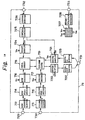
- Figs. 19 to 27 show this embodiment in which the present invention is implemented in a flash memory.
- reference numeral 711 denotes a flash memory (hereinafter, EEPROM).
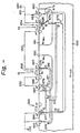
- the EEPROM 711 comprises a row address buffer 712, a column address buffer 713, a row pre-decoder 714, a column pre-decoder 715, a row decoder 716, a column decoder 717, a memory cell array 718, a column gate 719, a sense amplifier 720, a write amplifier 721, a data-out buffer 722, a data-in uffer 723, an erase amplifier 723, a control circuit 725, a control buffer 726, an internal power switching circuit 727, and a high-voltage detector 728.
- 729 denotes a row address signal terminal for handling multiple bits
- 730 denotes a column address signal terminal for handling multiple bits
- 731 denotes a data-in/out terminal
- 732 denotes a control signal terminal for handling various control signals
- 733 denotes a high-voltage power (Vpp) terminal for writing.
- the internal power switching circuit 727 selects either of external supply voltages Vcc and Vpp according to the output of the high-voltage detector 728, and outputs the selected voltage as an internal supply voltage V PI .
- the internal supply voltage V PI is supplied to each of the row decoder 716, column decoder 717, write amplifier 721, and erase amplifier 724.
- Fig. 20 shows components of the row decoder 716.
- nMOS n-channel MOS
- nMOS transistors 760 to 762 which receive signals from the row pre-decoder 714 to the gates thereof, and an nMOS transistor 763 serving as a load element are connected between the internal supply voltage (V PI ) terminal and ground (0 V) terminal.
- CMOS inverter gate 716a made up of a p-channel MOS (hereinafter; pMOS) transistor 764 and an nMOS transistor 765 represents the internal supply voltage V PI .
- the output (V PI or 0 V) of the CMOS inverter gate 716a is connected to a word line in a memory cell array 718, and supplied to control gates of memory transistors, which are arranged in a row in the memory cell array 718, via the word line.
- Fig. 21 shows components of the column decoder 717.
- multiple nMOS transistors 766 and 767 which receive signals from the column pre-decoder 715 to the gates thereof, as well as a nMOS transistor 768 serving as a load element are connected between the internal supply voltage (V PI ) terminal and ground (0 V) terminal.
- V PI internal supply voltage
- nMOS transistors 766 and 767 are all on; that is, the signals from the column pre-decoder 715 are all high
- the output of a CMOS inverter gate 717a made up of a pMOS transistor 769 and an nMOS transistor 770 represents the internal supply voltage V PI .
- the output of the CMOS inverter gate 717a (V PI or 0 V) is supplied to the gate of a transistor for selecting a bit line in the column gate 719.
- Fig. 22 shows components of the write amplifier 721.
- the write amplifier 721 two nMOS transistors 771 and 772, which are turned on when a signal sent from the control circuit 725 to represent a write mode and write data fetched from the data-in buffer 723 are both high, and an nMOS transistor 773 serving as a load element are connected between the internal supply voltage (V PI ) terminal and ground (0 V) terminal.
- the write amplifier 721 further includes a CMOS inverter gate 721a made up of a pMOS transistor 774 and an nMOS transistor 775, and an nMOS transistor for output.
- the internal supply voltage V PI is supplied to a bit line specified by the column gate 719 via the output transistor 776.
- Fig. 23 shows components of the erase amplifier 724.
- an nMOS transistor 777 which is turned on in response to a high-level signal that is sent from the control circuit 725 and represents an erase mode
- an nMOS transistor 778 serving as a load element are connected between an internal supply voltage (V PI ) terminal and a ground (0 V) terminal.
- a CMOS inverter gate 724a made up of a pMOS transistor 779 and an nMOS transistor 780, a CMOS inverter gate 724b made up of a pMOS transistor 781 and nMOS transistor 782, and a CMOS inverter gate 724c made up of a pMOS transistor 783 and an nMOS transistor 784 are connected between the internal supply voltage (V PI ) terminal and ground (0 V) terminal.
- V PI internal supply voltage
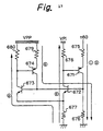
- Figs. 24 and 25 show components of the internal power switching circuit 727 and high-voltage detector 728 respectively.
- B1 and B2 in Fig. 24, as well as B3 and B4 in Fig. 25 denote four blocks constituting the internal power switching circuit 727.
- the block B1 has the same circuitry as that in Fig. 18. The same reference numerals as those in Fig. 18 are used.
- Reference numeral 701 denotes a power line (first power line) for an external power supply Vcc; 702 denotes a power line (second power line) for an internal power supply V PI ; 703 denotes a power line for an external power supply Vpp (where, Vpp > Vcc); 704 denotes a first n-channel MOS transistor one of whose drain and source electrodes is connected to the first power line 701, and the other of whose drain and source electrodes is connected to the second power line 702; 703 denotes a second p-channel MOS transistor one of whose drain and source electrodes and whose well are connected to a third power line 703, and the other of whose drain and source electrodes is connected to a node n70; 706 denotes a third p-channel MOS transistor one of whose drain and source electrodes is connected to the node n70 and the other of whose drain and source electrodes and whose well are connected to the second power line 702; and 707 denotes
- the blocks B2 to B4 generate signals G1, G2, and G3 for controlling the on or off operations of the MOS transistors 704 to 707.
- the block B3 generates the signal G1 whose logical amplitude ranges from 0 V to Vcc and the signal G4 whose logical amplitude ranges from 0 V to Vpp in response to an output of the high-voltage detector 728.
- the block B4 generates a delay signal G2 for the signal G4.
- the high-voltage detector 728 When the voltage Vpp exceeds the voltage Vcc at least by the sum of a threshold voltage Vth of a pMOS transistor 785 and a threshold voltage Vth of a pMOS transistor 786 (Vpp > Vcc), the high-voltage detector 728 provides a high-level signal equivalent to Vpp - 2Vth as an output of a CMOS inverter gate 728a made up of the pMOS transistor 786 and nMOS transistor 787, and outputs the high-level signal via two-stage inverter gates 728b and 728c with the phase unchanged.
- the block B3 When the output of the high-voltage detector 728 is high; that is, Vpp is larger than Vcc, the block B3 provides a low-level signal for two output node a and b of a state hold circuit 748 made up of a NOR gate 734, a NAND gate 735, inverter gates 736 and 737, and capacitors 821 and 822.
- the block B3 then fetches a signal from the node a via two-stage inverter gates 738 and 739 with the phase unchanged, and outputs the signal as a signal G 1 .
- the block B3 also fetches another signal from the other node b via four-stage inverter gates 740 to 743 with the phase unchanged, and outputs the signal as a signal G 4 .
- 790 to 793 denote nMOS transistors.
- 794 to 797 denote pMOS transistors.
- the supply voltage of the inverter gate 739 is Vcc or ground (0 V).
- the logical amplitude of the signal G1 ranges from 0 V to Vcc.
- the supply voltage of the inverter gate 741, 742, or 743 is Vpp or ground.
- the logical amplitude of the signal G4 ranges from 0 V to Vpp.
- the logical amplitude of a signal G2 fetched from the block B4 which is not shown also ranges from 0 V to Vpp.
- Vpp is larger than Vcc
- the signals G1, G2, and G4 are all 0 V.
- Vpp is not larger than Vcc, the signal G1 is equivalent to Vcc and the signals G2 and G4 are equivalent to Vpp.
- the block B2 constitutes a known bootstrap circuit, and generates a signal G3 whose logical amplitude is an extended one of the logical amplitude of the signal G4 ranging from 0 V to Vpp (180° out of phase).
- 800 to 810 denote nMOS transistors; 811 to 814 denote pMOS transistors; 830 and 831 denote capacitors; 744 denotes an inverter gate made up of transistors 805 and 811; 745 denotes an inverter gate made up of transistors 810 and 814; 746 denotes an inverter gate made up of transistors 808 and 813; and 747 denotes an inverter gate made up of transistors 807 and 812.
- Figs. 26A to 26G show wave forms indicating a process of generating a signal G3 in the block B2.
- the voltage at the output node n71 of the inverter gate 744 rises to Vpp.
- the voltage at the output node n72 of the inverter gate 745 drops to 0 V.
- Vpp - Vth Vth denotes a threshold voltage of the transistor 804.
- a capacitor 831 is charged with the voltage.
- charges are released from a capacitor 830 with the voltage fluctuation (VPP to 0 V) at the node n72.
- the voltage at the node n73 starts decreasing along the time constant curve defined by the capacitance of the capacitor 830 and the channel resistance of the transistor 809.
- the voltage at the node n73 becomes lower than the threshold value of the inverter gate 746, the voltage at the node n74 decreases to 0 V and the transistor 806 is turned off.
- Vpp - 2Vth denotes a threshold voltage of the transistors 804 and 800.
- Vth denotes a threshold voltage of the transistors 804 and 800.
- the voltage at the node n75 becomes Vpp and the voltage at the node n76 rises to a voltage provided by adding a voltage across the capacitor 831 to the voltage at the node n75.
- the signal G3 whose logical amplitude is an extended one of the logical amplitude of the signal G4 ranging from 0 V to Vpp (herein, 0 V to Vpp + Vth) is generated.
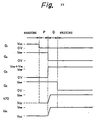
- Fig. 27 shows wave forms representing an operation of the block B1; that is, a process of switching the level of an internal supply voltage V PI at the time of transition from the read mode to write mode.
- the signal G1 is Vcc
- the signal G2 is Vpp
- the signal G3 is 0 V. Only the transistor 704 is on. During the read-mode period, V PI is therefore equal to Vcc.
- the signal G1 is set to 0 V
- the transistor 704 is turned off
- the transistor 706 is turned on
- V PI thus remains equal to Vcc.
- the signal G4 is set to 0 V
- the signal G3 is raised to Vpp + Vth
- the transistor 707 is turned on. This causes current to flow from the third power line 703 to the second power line 702.
- the voltage at the transistor 707 rises to V PI + Vpp for the Q period.
- the voltage at the node n70 during the Q period is V PI ; that is, Vpp.
- V PI The potential difference between the source and drain of the transistor 705 is 0 V. Even when the signal G2 is set to 0 V, a large current will not flow through the transistor 705 immediately.
- the potential difference between the p-channel diffused layer and n-type well in the source (node n70) of the transistor 706 becomes 0 V. Substrate current that causes a latch-up phenomenon does not flow, either.
- the cell current flows uninterruptedly from the third power supply 703 through the transistor 705, node n70, transistor 706, second power supply, etc., to the memory cell array 718.
- the high-voltage level of the signal G3 is set to Vpp + Vth so that the V PI value will become a maximum voltage Vpp during the Q period.
- the high-voltage level of the signal G3 is not limited to Vpp + Vth.
- the high-voltage level of the signal G3 may be Vcc+ Vth, Vcc + Vth to Vpp + Vth, or Vpp + Vth or more, as long as the V PI value will be higher than Vcc during the Q period.
- Flash memories are expected to substitute for magnetic storages.
- the properties of flash memories that is, small size and light weight will prove very helpful.
- the flash memory For actual use in portable equipment in place of magnetic storage, the flash memory must further be innovated to achieve downsizing, an increase in operational speed, reduction in power consumption, and decrease in voltage requirements.
- Embodiments of the present invention can provide innovative flash memory and solve some of the problems obstructing the widespread use of the flash memory.
Landscapes
- Engineering & Computer Science (AREA)
- Microelectronics & Electronic Packaging (AREA)
- Physics & Mathematics (AREA)
- Computer Hardware Design (AREA)
- Mathematical Physics (AREA)
- Computing Systems (AREA)
- General Engineering & Computer Science (AREA)
- Nonlinear Science (AREA)
- Power Engineering (AREA)
- Electromagnetism (AREA)
- General Physics & Mathematics (AREA)
- Radar, Positioning & Navigation (AREA)
- Automation & Control Theory (AREA)
- Read Only Memory (AREA)
- Logic Circuits (AREA)
- Semiconductor Memories (AREA)
- Non-Volatile Memory (AREA)
- Dc-Dc Converters (AREA)
Abstract
Description
- The present invention relates to a so-called flash memory or a nonvolatile semiconductor memory from which existent information can be electrically erased concurrently or block by block. In particular, this invention is concerned with improvements in erasing a flash memory and improvements in the associated circuitry.
- In recent years, a variety of semiconductor memories such as an electrically erasable programmable read only memory (EEPROM), which can be rewritten by electrically erasing data stored therein, have been developed in the field of nonvolatile memories.
- The semiconductor memories are nonvolatile memories which are made rewritable by electrically erasing specified data previously written therein.
- As for this kind of nonvolatile memory, in consideration of the use as a substitute for a magnetic storage or the like, efforts have been made to increase the capacity and decrease the cost. For use in a portable information processing terminal or the like, however, it is required to lower the voltage requirements.
- Known semiconductor memories, which are nonvolatile memories that are made rewritable by erasing specified data previously written therein, include an erasable programmable read only memory (EPROM) and the EEPROM.
- The EPROM has the advantage of a small cell size. However, data erasing is a nuisance because ultraviolet light must be used to erase data. As for the EEPROM, data erasing is easy to do because data can be erased electrically. However, the cell size in the EEPROM is larger than that in the EPROM, which makes it difficult to increase the capacity of an EEPROM.
- As a semiconductor memory having the advantages of the foregoing memories, for example, what is referred to as a flash memory has been developed.
- The term "flash memory" will be adopted in the succeeding description.
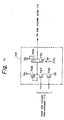
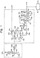
- The nonvolatile semiconductor memory has an overall configuration, for example, as that shown in Fig. 1. In Fig. 1,
N cell blocks 111 to 11N (for example, eight blocks) each having multiple transistor cells are arranged in a row. Thecell blocks 111 to 11N are provided with bit line selectcircuits 121 to 12N and sense amplifiers/sense buffers 131 to 13N respectively. - A row address signal is supplied from a row address buffer to each of the
cell blocks 111 to 11N via arow decoder 15. A column address signal is supplied from acolumn address buffer 16 to each of the bit line selectcircuits 121 to 12N via acolumn address decoder 17. A voltage VS sent from a sourcepower supply circuit 18 is applied to each of source electrodes of the transistor cells of thecell blocks 111 to 11N. - Fig. 2 shows the
cell block 11, one of the cells blocks in the aforesaid nonvolatile semiconductor memory, and its peripheral circuitry. In Fig. 2, components identical to those in Fig. 1 bear the same reference numerals, of which a description will be omitted. In Fig. 2, the bit lineselect circuit 12 comprises n-channel MOS field-effect transistors Q1 to Qn. Column address signals Y1 to Yn are fed from thecolumn decoder 17 to the gates of the transistors Q1 to Qn. - The
cell block 11 comprises a total of n by n field-effect transistors Q11 to Qnn having floating gates and control gates. The gates of n transistors Qil to Qin (where, i = 1, 2, etc., and n) arranged in tandem are provided with row address signals Xi sent from therow decoder 15 via word lines. - The drains of the n transistors Qli to Qni arranged in tandem are connected to the drains of the transistors Qi in the bit line
select circuit 12 via bit lines. Voltage from thesource power circuit 18 is applied to each of the sources of the transistors Qll to Qnn. Acell amplifier 13a and awrite buffer 13b are connected to each of the sources of the transistors Q1 to Qn. - In the foregoing semiconductor memory, when row addresses Xi and column addresses Yi are selected for writing, data read from the write buffer 13 are written in the transistors Qij of the
cell blocks 111 to 11N. Writing is performed simultaneously on one bit per each of thecell blocks 111 to 11N or a total of N bits designated with the row addresses and column addresses. Data erasing is performed concurrently on all transistors in thecell blocks 111 to 11N. - In a flash memory, information is retained depending on the presence or absence of a charge in a memory cell. Fig. 3 shows an example of a structure of a memory cell. As shown in Fig. 3, a gate has a two-layered structure consisting of a control gate (CG) 25 and a floating gate (FG) 24. The
control gate 25 is connected to a word line WLi and a drain (D) 23 is connected to a bit line BLi.Reference numeral 26 denotes a tunneling oxide film. - The flash memory is broadly divided into two types of what are referred to as NOR and NAND. These types differ from each other in a method of writing, reading, or erasing information into or from a memory cell. Taking the NOR type flash memory as an example, writing, reading, or erasing information into or from a memory cell will be described below.
- When information is to be written in a memory cell having the aforesaid structure, as shown in Fig. 4, the word line WLi is set to Vpp (approx. 12 V), the bit line BLi is set to approx. 6 V, and the source S is set to 0 V. High voltage is then applied to the control gate CG and drain D. Current then flows into the memory cell. Part of the electrons flowing through the memory cell are accelerated due to the high electric field in the vicinity of the drain D, gain energy, and then goes beyond the energy barrier of an insulating film of the floating gate. The electrons are finally injected into the floating gate FG. The floating gate FG is not electrically coupled with other circuits, so it therefore can retain charges on a semi-permanent basis.
- When information is to be read from a memory cell, as shown in Fig. 5, the word line WLi is set to Vcc (about 5 V), the bit line BLi is set to about 1 V, and the source S is set to 0 V. The memory cell is then selected by specifying the word line WLi and bit line BLi. The threshold value of the cell transistor varies depending on the charges retained in the floating gate FG. Current flowing through the selected memory cell varies depending on the information stored therein. The information therefore can be read out by detecting and amplifying the current.
- The voltage levels of the control gate CG, drain D, source S, and substrate PS in the aforesaid operative states are set to the values listed in Table 1.
Voltages in modes in a prior art CG D S PS Reading Vcc to 1 V 0 V 0 V Writing Vpp to 6 V 0 V 0 V Erasing 0 V Float Vpp 0 V - When information is to be erased from a memory cell, as shown in Fig. 6, the word line WLi is set to about 0 V and the bit line BLi is opened. In this state, the drain D is opened, about 0 volt is applied to the control gate CG, and a high voltage of about 12 volts is applied to the source S.
- Since a high voltage is applied to the source S, deep diffusion is required in order to increase the resistivity of the diffused layer in the source. This hinders reduction in cell area.
- For divided erasing, it is required that the Vss line in the source must partly have a different voltage. This leads to disconnection or an increased number of drive circuits. Eventually, chip size increases.
- A solution to the above problem is to apply a negative voltage to the word line WLi. To be more specific, as shown in Fig. 7, a negative voltage (about - 10 V) is applied to the control gate CG and Vcc (about 5 V) is applied to the source S. The drain D is opened. Erasing is then executed.
- In this case, since a low voltage is applied to the source S, the resistivity of the source need not be intensified. This contributes to reduction in cell size. Partial erasing is enabled by selectively applying negative voltage to the control gates CG.
- The aforesaid erasing method is a source erasing method in which charges in the floating gate FG are routed to the source. A channel erasing method is also available, wherein charges in the floating gate are routed to a channel; that is, a substrate. Even in this method, negative voltage is applied to the control gate. The channel erasing method is sometimes employed for the aforesaid NAND-type flash memory.
- Figs. 8 to 11 show the states of a memory cell with voltage applied according to various erasing methods. In Figs. 8 to 11, the memory cell is an n-channel transistor.
- Fig. 8 shows a state in which positive voltage is applied according to a channel erasing method. The drain D and source S are opened, and the control gate CG is set to 0 V. The high voltage Vpp is applied to the P well equivalent to a channel. In channel erasing, a triple-well structure shown in Fig. 8 is adopted because positive bias is applied to the channel.
- Fig. 9 shows a state in which a positive voltage is applied according to the source erasing method. The drain D is opened, and then the control gate CG is set to 0 V. The high voltage Vpp is applied to the source S. The substrate is opened or set to 0 V.
- Fig. 10 shows a state in which a negative voltage is applied according to the channel erasing method. The drain D and source S are opened, and the control gate CG is set to a negative voltage VBB. A positive voltage Vcc is applied to the p well equivalent to a channel. VBB - Vcc is applied between the control gate CG and channel.
- Fig. 11 shows a state in which negative voltage is applied according to the source erasing method. The drain D is opened, and then the control gate CG is set to the negative voltage VBB. The source S is set to the positive voltage Vcc.
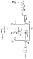
- A flash memory includes an internal power switching circuit for switching supply voltages depending on a mode. A previously-proposed internal power switching circuit has a simple circuitry but is likely to cause a latch-up phenomenon. The switching speed is decreased in order to avoid the latch-up phenomenon. This contradicts efforts to speeding up processing.
- Accordingly, it is desirable to realize an internal power switching circuit that can operate at a high speed with simple circuitry.
- According to an embodiment of an aspect of the present invention there is provided an internal power switching circuit for use in a flash memory or the like, comprising a first MOS transistor of a first polarity one of whose drain and source electrodes is connected to a first power line and the other of whose drain and source electrodes is connected to a second power line;
- a second MOS transistor of a second polarity one of whose drain and source electrodes and whose well are connected to a third power line having a higher voltage than the first power line, and the other one of whose drain and source electrodes is connected to a node; and
- a third MOS transistor of the second polarity one of whose drain and source electrodes is connected to the node and the other of whose drain and source electrodes is connected to the second power line. The internal power switching circuit further includes a fourth MOS transistor of the first polarity one of whose drain and source electrodes is connected to the third power line and the other of whose drain and source electrodes is connected to the second power line.
-
- In such an internal power switching circuit, when a low voltage is switched to a high voltage, the fourth MOS transistor assists in boosting the voltage of the second power line. This helps minimize the channel current in the second MOS transistor. A latch-up phenomenon can therefore be avoided.
- Reference will now be made, by way of example, to the accompanying drawings, in which:
- Fig. 1 shows an overall configuration of a flash memory in which the present invention is implemented;
- Fig. 2 is a circuit diagram showing a major section of Fig. 1;
- Fig. 3 shows a structure of a memory cell;
- Figs. 4 to 7 are explanatory diagrams for methods of reading, writing, and erasing a flash memory; Fig. 4 shows the conditions for writing; Fig. 5 shows the conditions for reading; Fig. 6 shows the conditions for erasing; Fig. 7 shows the conditions for erasing based on negative-voltage application;
- Fig. 8 is an explanatory diagram for channel erasing based on high-voltage application;
- Fig. 9 is an explanatory diagram for source erasing based on high-voltage application;
- Fig. 10 is an explanatory diagram for channel erasing based on negative-voltage application;
- Fig. 11 is an explanatory diagram for source erasing based on negative-voltage application;
- Fig. 12 shows a structure of a transistor cell;
- Fig. 13 is an explanatory diagram for excessive erasing;
- Fig. 14 shows an example of a previously-proposed internal power switching circuit;
- Fig. 15 shows waveforms showing the operations of Fig. 14;
- Fig. 16 is an explanatory diagram for occurrence of a latch-up;
- Fig. 17 is an equivalent circuit of Fig. 16;
- Fig. 18 is a configurational diagram showing the principle of an embodiment of the present invention;
- Fig. 19 is an overall block diagram showing a flash memory embodying the invention;
- Fig.20 shows components of a row decoder in the Fig. 19 embodiment;
- Fig. 21 shows components of a column decoder in the Fig. 19 embodiment;
- Fig. 22 shows components of a write amplifier in the Fig. 19 embodiment;
- Fig.23 shows components of an erase amplifier in the Fig. 19 embodiment;
- Fig. 24 shows components of blocks B1 and B2 of an internal power switching circuit in the Fig. 19 embodiment;
- Fig. 25 shows components of blocks B3 and B4 of the high-voltage detector and internal power switching circuit in the Fig. 19 embodiment;
- Figs. 26A to 26G show waves indicating the process of producing a signal G3 in the block B2 of the internal power switching circuit in the Fig. 19 embodiment; and
- Fig. 27 shows waveforms representing the operations of the block B1 of the internal power switching circuit in the Fig. 19 embodiment. Prior to an embodiment, pre-erase writing will be described.
-
- Fig. 12 shows a structure of a memory cell shown in Fig. 3 in more detail. A transistor serving as the memory cell has, as shown in Fig. 12, such a structure that n-type
diffusive regions type substrate 31 with a certain space between them. A floating gate (FG) 34 and a control gate (CG) 35 are formed above the p-type substrate 31, and coated with anoxide film 36. The n-typediffusive regions source electrode 37 and adrain electrode 39 respectively. Thecontrol gate 35 is coupled with agate electrode 38. - An insulating film for isolating between the floating gate (FG) and control gate (CG) in the stacked gate type memory cell transistor may be an oxide film or oxide nitride film. However, an ONO film; that is, a three-layered structure of an oxide film over a nitride film over an oxide film is preferred in an effort to prevent a time-sequential leakage of charges from the floating gate (FG). Using the same process for producing the insulating film between gate electrodes, an insulating film for a gate in a single gate-type transistor which is used in any region of peripheral circuits may be produced.
- In this case, the gate insulating film for the single gate-type transistor formed in a region of peripheral circuits may be the ONO film or oxide nitride film. The gate insulating films for transistors except memory cell transistors are not necessarily oxide films.
- Writing in a memory cell is achieved by injecting electrons into the floating gate (FG) 34, whereby "0" will be written. Erasing is achieved by removing electrons from the floating gate (FG) 34, whereby "1" will be written.
- When a source erasing method based on high-voltage application is performed to erase the transistor cell (to write "1"), as described previously, high voltage is applied to the
source electrode 37, zero volt is applied to thegate electrode 38, and thedrain electrode 39 is opened. The electrons retained in the floatinggate 34 are thus removed. - When "0" has been written in the transistor cell; that is, when electrons have been retained in the floating
gate 34, the threshold for the cell, I, in Fig. 13 decreases to be lower than a threshold level for identifying data "1" for the period of an erasing time T. - In contrast, when "1" has been written in the transistor cell; that is, when no electrons have been retained in the floating
gate 34, since the threshold level is low, as the threshold of the cell decreases as indicated with II in Fig. 13 due to the erasing, the threshold level becomes 0 for a shorter period of time than the erasing time T. During the above erasing, too many electrons are removed from transistor cells in which "1s" have been written. The transistor cells consequently enter a Normally On state. - In order to prevent the foregoing excessive erasing, it is necessary for a flash memory, in which cells are NORed, to write data "0" in each of the transistor cells in all cell blocks before concurrent erasing is performed. Writing data "0" is performed on all transistor cells, wherein the data values written in the transistor cells are not checked. Specifically, a source voltage Vs for the
source electrode 37 in the transistor cell shown in Fig. 12 is set to 0 V, a gate voltage Vg for thegate electrode 38 is set to a high voltage, and a drain voltage VD for thedrain electrode 39 is set to a high voltage. High-energy electrons developed by applying high voltage between the source and drain then reach the floating gate 84 through theoxide film 36. Data "0" is thus written in the transistor cell. - As apparent from the previous description, in a flash memory, the electrode voltages of a memory cell transistor differ from the read mode to the write (or erase) mode. Therefore, the internal supply voltage must be changed for each mode.
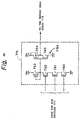
- Fig. 14 shows the components of a typical previously-proposed internal power switching circuit.
-
Reference numeral 650 denotes a power line (hereinafter, external power line) on which an external power supply Vcc of, for example, + 5 V is placed. 651 denotes a power line (hereinafter, external power line) on which an external power supply Vpp of, for example, +12 V is placed; and 652 denotes a power line (hereinafter, internal power line) for an internal power supply VPI that is connected to a control electrode of a memory cell transistor via a row decoder which is not shown. - A
MOS transistor 653, which is turned on when a signal G1 is high, is connected between theexternal power line 650 andinternal power line 652. AMOS transistor 654, which is turned on when a signal G2 is low, and aMOS transistor 655, which is complementary to thetransistor 653, that is, which turned on when thetransistor 653 is off, are connected in series with each other via a node n60. TheMOS transistor 653 is of the n-channel depletion type, and theMOS transistors transistor 654 is connected to theexternal power line 651, and the well (n type) of thetransistor 655 is connected to theinternal power line 652. - According to the foregoing circuitry, when the signals G1 and G2 are driven high, the
transistor 653 is turned on and thetransistors external power line 650 is reflected in theinternal power line 652. On the contrary, when the signals G1 and G2 are driven low, thetransistor 653 is turned off and thetransistors internal power line 652. When the levels of the signals G1 and G2 are controlled for each of read and write modes, an internal supply voltage VPI representing a voltage (Vcc or Vpp) suitable for each mode can be generated. - Fig. 15 is an example of an actual timing chart for the Figure 14 circuit. In read mode, the signal G1 is high (Vcc of + 5 V) and the signal G2 is high (Vpp of + 12 V). As a result, VPI equals to Vcc (+ 5 V).
- For transition to the write mode, first, the signal G1 is driven low. This turns off the
transistor 653 and turns on thetransistor 655. Thereafter, the level of the signal G2 is decreased gradually to be low. The voltage at the node n60 becomes VPI (+ 5 V) because thetransistor 655 is turned on. After time elapses, when the level of the signal G2 decreases to such an extent that thetransistor 654 is turned on, theexternal power line 651 and node n60 are connected to each other via thetransistor 654. The node n60 is connected to theinternal power line 652 via thetransistor 655 which has already been turned on. Current therefore flows from theexternal power line 651 to theinternal power line 652. Eventually, VPI is switched to Vpp (+ 12 V). - In transition to the write mode, the level of the signal G2 is decreased gradually. The reason will be described below.
- That is to say, when the level of the signal G2 (gate level of the transistor 654) is driven low (0 v) quickly, an enormous channel current ich2 proportional to a difference between the Vpp (+ 12 V) and gate level (0 V) flows through the
transistor 654. At this time, only a limited channel current ich3 proportional to a relatively small difference between the voltage at the node n60 (+ 5 V) and gate level (0 V) flows through thetransistor 655. A residual current (ich2 - ich3) flows from the p-channel diffused layer in the source region (node n60) of thetransistor 655 into the n-type well. A large substrate current then develops. - As a result, a parasitic pnpn thyristor is turned on, and a MOS device is held at low impedance. Thus a fatal phenomenon; that is, a latch-up phenomenon is likely to occur.
- A mechanism for causing a latch-up will be described briefly. Fig. 16 shows the structure of that portion of the internal power switching circuit in Fig. 14, corresponding to the
transistors - When the signal G1 is 0 V, the signal G2 changes from Vpp to 0 V. Currents iQ2 and iQ3 flow. When the node n60 floats by about 0.7 V or more from the n-type well 662 whose voltage is VPI, the p+n junction is biased in the forward direction. Holes are injected from the p+-type region into the n-type well 662 along a
route 1. The holes are minority carriers within the n-type well. When diffused, the holes reach the well boundary and flow into the p-type substrate 660. Within the p-type substrate 660, the holes behave as majority carriers and flow into a p+-type contact 669. - At this time, a
resistor 676 placed between the p+-type contact 669 and asource n + 668 of an n-channel transistor 680 located on the other periphery causes the substrate voltage to partly rise. When the substrate voltage arising near thesource n + 668 rises by about 0.7 V, the n+p junction is biased in the forward direction. As a result, electrons are injected from thesource n + 668 to the p-type substrate 660 as indicated with 2. When diffused, the electrons reach the well boundary and flow into acontact n + 667 of the n-type well 662. The voltage drop resulting from the current and resistance of theresistor 678 causes the voltage of the n-type well near asource p + 665 of a p-channel transistor 655 to decrease. The p+n junction is then biased in the forward direction. Holes are injected again from thesource p + 665 into the n-type well 662. This increases substrate current. Positive feedback is thus repeated. - Due to the rise in substrate voltage, electrons injected from the n+-
type source 668 to the p-type substrate 660 are diffused to move within the p-type substrate, and then flow into the n-type well 661 whose voltage is VPP. Within the n-type well 661, electrons flow as majority carriers into an n+-type source 663. The voltage of the n-type well 661 partly decreases because of a voltage drop caused by aresistor 679 located between the contact of the n+-type source 663 and the p+-type source 664 of a p-channel transistor 654. When the voltage of the n-type well 661 in the vicinity of the p+-type source 664 drops by about 0.7 V, the p+n junction is biased in the forward direction. As a result, holes are injected from the p+-type source 664 to the n-type well 660 as indicated by 5. The holes reach the well boundary while diffusing, and then flow into the contact of the p-type substrate 660 with the p+-type source 669. The current and resistance of theresistor 676 boost the substrate voltage. - Consequently, the n+p junction is biased in the forward direction. Electrons are injected from the n+-type source to the p-type substrate again as indicated with 4. Positive feedback is thus repeated.
- As a result, overcurrent steadily flows from the external power supply line Vpp to VSS. This causes a latch-up.
- In some previously-proposed circuits, the level of the signal G2 is decreased gradually in order to avoid an abrupt increase in channel current ich2. Substrate current is thus minimized to prevent occurrence of a latch-up phenomenon.
- However, in this kind of previously-proposed internal power switching circuit for a semiconductor memory, a latency time must be present between the read and write modes in order to avoid a latch-up phenomenon. The latency time includes the time constant for decreasing the level of the signal G1 and the time for absorbing a manufacturing error of each transistor. Mode change cannot be speeded up, which has obstructed realization of a high-speed external memory that is freely rewritable.
- An internal power switching circuit embodying the present invention can resolve the aforesaid problems and can prove effective for a flash memory or any other semiconductor memory in which the voltage levels of an internal power supply are switched.
- Fig. 18 is an explanatory diagram showing a principle of an internal power switching circuit embodying the present invention. As shown in Fig. 18,the internal power switching circuit comprises:a first n-
channel MOS transistor 704, one of whose drain and source electrodes is connected to afirst power line 701, and the other one of whose drain and source electrodes is connected to asecond power line 702; a second p-channel MOS transistor 705,one of whose drain and source electrodes as well as whose well are connected to athird power line 703 of a voltage Vpp that is higher than the voltage Vcc of thefirst power line 701, and the other of whose drain and source electrodes is connected to a node n70; and a third p-channel MOS transistor 706, one of whose drain and source electrodes is connected to the node n 70 and the other of whose drain and source electrodes as well as whose well are connected to thesecond power line 702. The internal power switching circuit further includes a fourth n-channel MOS transistor 707 one of whose drain and source electrodes is connected to thethird power line 703 and the other of whose drain and source electrodes is connected to thesecond power line 702. - In the foregoing circuit, if the n-
channel transistor 707 is turned on during transition from the read mode to write mode, the voltage VPI of thesecond power line 702 is lifted via the n-channel transistor 707 and exceeds the voltage Vcc of the first power line 702 (the lift-up voltage depends on the gate voltage of the n-channel transistor 707). The lifted VPI is transmitted to the node n70 via the p-channel transistor 706 that is on. - During mode transition, the voltage at the node n70 is boosted to exceed at least Vcc. The drain-source voltage (equivalent to a potential difference between the n70 and Vpp) can therefore be decreased to minimize the channel current of the p-
channel transistor 705. Furthermore, the gate-source voltage (equivalent to a potential difference between G1 and n1) of the p-channel transistor 706 can be increased to expand the channel current-carrying capacity of the p-channel transistor 706. As a result, the channel current in the p-channel transistor 706 is balanced with the channel current in the p-channel-transistor 705. Consequently, substrate current is minimized to prevent occurrence of a latch-up phenomenon reliably. - In such an internal power switching circuit even when the gate level of the p-
channel transistor 705 is driven low abruptly, a latch-up phenomenon does not occur. The latency time at the time of mode transition can be minimized to be equal to the time required to lift up the level of the node n70. Such a circuit can thus provide an internal power switching art helpful in realizing a high-speed external memory that can be freely rewritable. - An embodiment of the present invention will be described in conjunction with the drawings.
- Figs. 19 to 27 show this embodiment in which the present invention is implemented in a flash memory.
- To begin with, the configuration will be described. In Fig. 19,
reference numeral 711 denotes a flash memory (hereinafter, EEPROM). TheEEPROM 711 comprises arow address buffer 712, acolumn address buffer 713, arow pre-decoder 714, acolumn pre-decoder 715, arow decoder 716, acolumn decoder 717, amemory cell array 718, acolumn gate 719, asense amplifier 720, awrite amplifier 721, a data-outbuffer 722, a data-inuffer 723, an eraseamplifier 723, acontrol circuit 725, acontrol buffer 726, an internalpower switching circuit 727, and a high-voltage detector 728. Also in the figure, 729 denotes a row address signal terminal for handling multiple bits; 730 denotes a column address signal terminal for handling multiple bits; 731 denotes a data-in/out terminal; 732 denotes a control signal terminal for handling various control signals; and 733 denotes a high-voltage power (Vpp) terminal for writing. - The internal
power switching circuit 727 selects either of external supply voltages Vcc and Vpp according to the output of the high-voltage detector 728, and outputs the selected voltage as an internal supply voltage VPI. In this example, the internal supply voltage VPI is supplied to each of therow decoder 716,column decoder 717, writeamplifier 721, and eraseamplifier 724. - Fig. 20 shows components of the
row decoder 716. In therow decoder 716, multiple n-channel MOS (hereinafter, nMOS)transistors 760 to 762, which receive signals from therow pre-decoder 714 to the gates thereof, and annMOS transistor 763 serving as a load element are connected between the internal supply voltage (VPI) terminal and ground (0 V) terminal. When thetransistors 760 to 762 are all on; that is, when the signals from therow pre-decoder 714 are all high, the output of aCMOS inverter gate 716a made up of a p-channel MOS (hereinafter; pMOS)transistor 764 and annMOS transistor 765 represents the internal supply voltage VPI. The output (VPI or 0 V) of theCMOS inverter gate 716a is connected to a word line in amemory cell array 718, and supplied to control gates of memory transistors, which are arranged in a row in thememory cell array 718, via the word line. - Fig. 21 shows components of the
column decoder 717. In thecolumn decoder 717,multiple nMOS transistors 766 and 767, which receive signals from thecolumn pre-decoder 715 to the gates thereof, as well as anMOS transistor 768 serving as a load element are connected between the internal supply voltage (VPI) terminal and ground (0 V) terminal. When thenMOS transistors 766 and 767 are all on; that is, the signals from thecolumn pre-decoder 715 are all high, the output of aCMOS inverter gate 717a made up of apMOS transistor 769 and annMOS transistor 770 represents the internal supply voltage VPI. The output of theCMOS inverter gate 717a (VPI or 0 V) is supplied to the gate of a transistor for selecting a bit line in thecolumn gate 719. - Fig. 22 shows components of the
write amplifier 721. In thewrite amplifier 721, twonMOS transistors 771 and 772, which are turned on when a signal sent from thecontrol circuit 725 to represent a write mode and write data fetched from the data-inbuffer 723 are both high, and annMOS transistor 773 serving as a load element are connected between the internal supply voltage (VPI) terminal and ground (0 V) terminal. Thewrite amplifier 721 further includes a CMOS inverter gate 721a made up of apMOS transistor 774 and annMOS transistor 775, and an nMOS transistor for output. When the twonMOS transistors 771 and 772 are turned on, the internal supply voltage VPI is supplied to a bit line specified by thecolumn gate 719 via theoutput transistor 776. - Fig. 23 shows components of the erase
amplifier 724. In the eraseamplifier 724, an nMOS transistor 777, which is turned on in response to a high-level signal that is sent from thecontrol circuit 725 and represents an erase mode, and an nMOS transistor 778 serving as a load element are connected between an internal supply voltage (VPI) terminal and a ground (0 V) terminal. A CMOS inverter gate 724a made up of a pMOS transistor 779 and an nMOS transistor 780, a CMOS inverter gate 724b made up of a pMOS transistor 781 and nMOS transistor 782, and a CMOS inverter gate 724c made up of a pMOS transistor 783 and an nMOS transistor 784 are connected between the internal supply voltage (VPI) terminal and ground (0 V) terminal. When the nMOS transistor 777 is on, the internal supply voltage VPI is supplied to all source electrodes of memory cell transistors in thememory cell array 718. - Figs. 24 and 25 show components of the internal
power switching circuit 727 and high-voltage detector 728 respectively. B1 and B2 in Fig. 24, as well as B3 and B4 in Fig. 25 denote four blocks constituting the internalpower switching circuit 727. The block B1 has the same circuitry as that in Fig. 18. The same reference numerals as those in Fig. 18 are used. -
Reference numeral 701 denotes a power line (first power line) for an external power supply Vcc; 702 denotes a power line (second power line) for an internal power supply VPI; 703 denotes a power line for an external power supply Vpp (where, Vpp > Vcc); 704 denotes a first n-channel MOS transistor one of whose drain and source electrodes is connected to thefirst power line 701, and the other of whose drain and source electrodes is connected to thesecond power line 702; 703 denotes a second p-channel MOS transistor one of whose drain and source electrodes and whose well are connected to athird power line 703, and the other of whose drain and source electrodes is connected to a node n70; 706 denotes a third p-channel MOS transistor one of whose drain and source electrodes is connected to the node n70 and the other of whose drain and source electrodes and whose well are connected to thesecond power line 702; and 707 denotes a fourth n-channel MOS transistor one of whose drain and source electrodes is connected to thethird power line 703 and the other of whose drain and source electrodes is connected to thesecond power line 702. The fourth n-channel MOS transistor 707 is a key circuit element in this embodiment. - The blocks B2 to B4 generate signals G1, G2, and G3 for controlling the on or off operations of the
MOS transistors 704 to 707. The block B3 generates the signal G1 whose logical amplitude ranges from 0 V to Vcc and the signal G4 whose logical amplitude ranges from 0 V to Vpp in response to an output of the high-voltage detector 728. The block B4 generates a delay signal G2 for the signal G4. - When the voltage Vpp exceeds the voltage Vcc at least by the sum of a threshold voltage Vth of a
pMOS transistor 785 and a threshold voltage Vth of a pMOS transistor 786 (Vpp > Vcc), the high-voltage detector 728 provides a high-level signal equivalent to Vpp - 2Vth as an output of aCMOS inverter gate 728a made up of thepMOS transistor 786 andnMOS transistor 787, and outputs the high-level signal via two-stage inverter gates - When the output of the high-
voltage detector 728 is high; that is, Vpp is larger than Vcc, the block B3 provides a low-level signal for two output node a and b of astate hold circuit 748 made up of a NORgate 734, aNAND gate 735,inverter gates capacitors stage inverter gates stage inverter gates 740 to 743 with the phase unchanged, and outputs the signal as a signal G4. 790 to 793 denote nMOS transistors. In the figure, 794 to 797 denote pMOS transistors. - The supply voltage of the
inverter gate 739 is Vcc or ground (0 V). The logical amplitude of the signal G1 ranges from 0 V to Vcc. The supply voltage of theinverter gate 741, 742, or 743 is Vpp or ground. The logical amplitude of the signal G4 ranges from 0 V to Vpp. The logical amplitude of a signal G2 fetched from the block B4 which is not shown also ranges from 0 V to Vpp. When Vpp is larger than Vcc, the signals G1, G2, and G4 are all 0 V. When Vpp is not larger than Vcc, the signal G1 is equivalent to Vcc and the signals G2 and G4 are equivalent to Vpp. - The block B2 constitutes a known bootstrap circuit, and generates a signal G3 whose logical amplitude is an extended one of the logical amplitude of the signal G4 ranging from 0 V to Vpp (180° out of phase). In Fig. 24, 800 to 810 denote nMOS transistors; 811 to 814 denote pMOS transistors; 830 and 831 denote capacitors; 744 denotes an inverter gate made up of
transistors transistors transistors transistors 807 and 812. - Figs. 26A to 26G show wave forms indicating a process of generating a signal G3 in the block B2. In these waveforms, when the signal G4 drops, the voltage at the output node n71 of the inverter gate 744 rises to Vpp. At the same time, the voltage at the output node n72 of the
inverter gate 745 drops to 0 V. With the voltage fluctuation at the node n71, the voltage at the node n76 rises to Vpp - Vth (Vth denotes a threshold voltage of the transistor 804). Acapacitor 831 is charged with the voltage. On the other hand, charges are released from acapacitor 830 with the voltage fluctuation (VPP to 0 V) at the node n72. The voltage at the node n73 starts decreasing along the time constant curve defined by the capacitance of thecapacitor 830 and the channel resistance of thetransistor 809. When the voltage at the node n73 becomes lower than the threshold value of theinverter gate 746, the voltage at the node n74 decreases to 0 V and the transistor 806 is turned off. - When the transistor 806 is turned off, the voltage at the node n75 rises to Vpp - 2Vth (2Vth denotes a threshold voltage of the
transistors 804 and 800). This causes the voltage at the node n76 to rise to a voltage to which a voltage across thevoltage capacitor 831 at the node n75 is added. That is to say, when the voltage at the node n76 rises, the voltage at the node n75 rises to a value provided by subtracting Vth (Vth denotes a threshold voltage of the transistor 800) from the voltage at the node n76. Eventually, the voltage at the node n75 becomes Vpp and the voltage at the node n76 rises to a voltage provided by adding a voltage across thecapacitor 831 to the voltage at the node n75. As a result, the signal G3 whose logical amplitude is an extended one of the logical amplitude of the signal G4 ranging from 0 V to Vpp (herein, 0 V to Vpp + Vth) is generated. - Fig. 27 shows wave forms representing an operation of the block B1; that is, a process of switching the level of an internal supply voltage VPI at the time of transition from the read mode to write mode.
- In Fig. 27, during the read-mode period, the signal G1 is Vcc, the signal G2 is Vpp, and the signal G3 is 0 V. Only the
transistor 704 is on. During the read-mode period, VPI is therefore equal to Vcc. - For shifting to the write mode, during the P period, the signal G1 is set to 0 V, the
transistor 704 is turned off, and thetransistor 706 is turned on, and VPI thus remains equal to Vcc. The voltage at the node n70 is raised to Vpp (= Vcc) via thetransistor 706. During the Q period, the signal G4 is set to 0 V, the signal G3 is raised to Vpp + Vth, and thetransistor 707 is turned on. This causes current to flow from thethird power line 703 to thesecond power line 702. The voltage at thetransistor 707 rises to VPI + Vpp for the Q period. - The voltage at the node n70 during the Q period is VPI; that is, Vpp. The potential difference between the source and drain of the
transistor 705 is 0 V. Even when the signal G2 is set to 0 V, a large current will not flow through thetransistor 705 immediately. The potential difference between the p-channel diffused layer and n-type well in the source (node n70) of thetransistor 706 becomes 0 V. Substrate current that causes a latch-up phenomenon does not flow, either. With the signal G2 held at 0 V, if writing of a memory cell is actually started, the cell current flows uninterruptedly from thethird power supply 703 through thetransistor 705, node n70,transistor 706, second power supply, etc., to thememory cell array 718. - As mentioned above, in this embodiment, even if the gate level of the
transistor 705 is decreased to 0 V abruptly, there is no possibility that a latch-up phenomenon will occur. The latency time required for transition from the read mode to write mode (equivalent to P + Q in Fig. 108) can be minimized to be as short as that required for stable operations of devices. This results in an internal power switching art permitting fast mode change and contributing to realization of a high-speed external memory that can be freely rewritable. - In the aforesaid embodiment , the high-voltage level of the signal G3 is set to Vpp + Vth so that the VPI value will become a maximum voltage Vpp during the Q period. The high-voltage level of the signal G3 is not limited to Vpp + Vth. Alternatively, the high-voltage level of the signal G3 may be Vcc+ Vth, Vcc + Vth to Vpp + Vth, or Vpp + Vth or more, as long as the VPI value will be higher than Vcc during the Q period.
- Through use of such an internal power switching circuit embodying the present invention, the latency time occurring at the transition from the read mode to write mode can be minimized. This results in, for example, an internal power switching art that contributes to realization of a high-speed external memory which can be rewritten freely.
- Flash memories are expected to substitute for magnetic storages. For use in portable equipment on behalf of magnetic storages, in particular, the properties of flash memories; that is, small size and light weight will prove very helpful. For actual use in portable equipment in place of magnetic storage, the flash memory must further be innovated to achieve downsizing, an increase in operational speed, reduction in power consumption, and decrease in voltage requirements. Embodiments of the present invention can provide innovative flash memory and solve some of the problems obstructing the widespread use of the flash memory.
Claims (3)
- An internal power switching circuit for a semiconductor memory, comprising:a first n-channel MIS transistor (704) one of whose drain and source electrodes is connected to a first power line (701) and the other of whose drain and source electrodes is connected to a second power line (702);a second p-channel MIS transistor (705) one of whose drain and source electrodes and whose well are connected to a third power line (703) the voltage (Vpp) of which is higher than the voltage (Vcc) on said first power line (701), and the other of whose drain and source electrodes is connected to a node (n70); anda third p-channel MIS transistor (706) one of whose drain and source electrodes is connected to said node (n70), and the other of whose drain and source electrodes, and whose well are connected to said second power line (702), further including:a fourth n-channel MIS transistor (707) one of whose drain and source electrodes is connected to said third power line (703) and the other of whose drain and source electrodes is connected to said second power line (702).
- An internal power switching circuit for a semiconductor memory according to claim 1, wherein:the on or off operations of said first MIS transistor (704) and third MIS transistor (706) are complementary to each other; andwhen said third transistor (706) is to be turned on, said fourth MIS transistor (707) is turned on simultaneously with or after the on operation of said third MIS transistor (706), and then said second MIS transistor (705) is turned on.
- An internal power switching circuit for a semiconductor memory according to claim 1 or 2, wherein the gate voltage of said fourth MIS transistor (707) during on operation is higher than a voltage resulting from the addition of a threshold value of the fourth MIS transistor (707) to the voltage (Vcc) of said first power line (701).
Applications Claiming Priority (17)
| Application Number | Priority Date | Filing Date | Title |
|---|---|---|---|
| JP32470191A JP3281008B2 (en) | 1991-12-09 | 1991-12-09 | Semiconductor storage device |
| JP32470191 | 1991-12-09 | ||
| JP34657191 | 1991-12-27 | ||
| JP34657191A JPH05182483A (en) | 1991-12-27 | 1991-12-27 | Nonvolatile semiconductor memory device |
| JP467892 | 1992-01-14 | ||
| JP467892A JPH05189984A (en) | 1992-01-14 | 1992-01-14 | Nonvolatile semiconductor memory device |
| JP6414392 | 1992-03-19 | ||
| JP6414392 | 1992-03-19 | ||
| JP4145300A JPH05343985A (en) | 1992-06-05 | 1992-06-05 | Exclusive or/exclusive nor logic circuit |
| JP14530092 | 1992-06-05 | ||
| JP15495892 | 1992-06-15 | ||
| JP15495892 | 1992-06-15 | ||
| JP25659492 | 1992-09-25 | ||
| JP25659492A JP3182917B2 (en) | 1992-09-25 | 1992-09-25 | Negative voltage bias circuit and semiconductor memory device |
| JP29998792A JP3119740B2 (en) | 1992-11-10 | 1992-11-10 | Internal power supply switching circuit for semiconductor memory |
| JP29998792 | 1992-11-10 | ||
| EP92924898A EP0570597B1 (en) | 1991-12-09 | 1992-12-09 | Flash memory improved in erasing characteristic, and circuit therefor |
Related Parent Applications (1)
| Application Number | Title | Priority Date | Filing Date |
|---|---|---|---|
| EP92924898A Division EP0570597B1 (en) | 1991-12-09 | 1992-12-09 | Flash memory improved in erasing characteristic, and circuit therefor |
Publications (3)
| Publication Number | Publication Date |
|---|---|
| EP0944094A2 EP0944094A2 (en) | 1999-09-22 |
| EP0944094A3 EP0944094A3 (en) | 1999-11-03 |
| EP0944094B1 true EP0944094B1 (en) | 2001-10-24 |
Family
ID=27571540
Family Applications (7)
| Application Number | Title | Priority Date | Filing Date |
|---|---|---|---|
| EP01117838A Withdrawn EP1168365A3 (en) | 1991-12-09 | 1992-12-09 | Negative-voltage bias circuit |
| EP99115180A Expired - Lifetime EP0961290B1 (en) | 1991-12-09 | 1992-12-09 | Flash memory with improved erasability and its circuitry |
| EP99110956A Expired - Lifetime EP0944094B1 (en) | 1991-12-09 | 1992-12-09 | Power switching circuit |
| EP99115179A Expired - Lifetime EP0961289B1 (en) | 1991-12-09 | 1992-12-09 | Flash memory with improved erasability and its circuitry |
| EP01121238A Withdrawn EP1168362A3 (en) | 1991-12-09 | 1992-12-09 | Flash memory with improved erasability and its circuitry |
| EP92924898A Expired - Lifetime EP0570597B1 (en) | 1991-12-09 | 1992-12-09 | Flash memory improved in erasing characteristic, and circuit therefor |
| EP99114223A Withdrawn EP0954102A1 (en) | 1991-12-09 | 1992-12-09 | Exclusive or/nor circuits |
Family Applications Before (2)
| Application Number | Title | Priority Date | Filing Date |
|---|---|---|---|
| EP01117838A Withdrawn EP1168365A3 (en) | 1991-12-09 | 1992-12-09 | Negative-voltage bias circuit |
| EP99115180A Expired - Lifetime EP0961290B1 (en) | 1991-12-09 | 1992-12-09 | Flash memory with improved erasability and its circuitry |
Family Applications After (4)
| Application Number | Title | Priority Date | Filing Date |
|---|---|---|---|
| EP99115179A Expired - Lifetime EP0961289B1 (en) | 1991-12-09 | 1992-12-09 | Flash memory with improved erasability and its circuitry |
| EP01121238A Withdrawn EP1168362A3 (en) | 1991-12-09 | 1992-12-09 | Flash memory with improved erasability and its circuitry |
| EP92924898A Expired - Lifetime EP0570597B1 (en) | 1991-12-09 | 1992-12-09 | Flash memory improved in erasing characteristic, and circuit therefor |
| EP99114223A Withdrawn EP0954102A1 (en) | 1991-12-09 | 1992-12-09 | Exclusive or/nor circuits |
Country Status (5)
| Country | Link |
|---|---|
| US (7) | US5608670A (en) |
| EP (7) | EP1168365A3 (en) |
| KR (1) | KR970003809B1 (en) |
| DE (4) | DE69232807T2 (en) |
| WO (1) | WO1993012525A1 (en) |
Cited By (1)
| Publication number | Priority date | Publication date | Assignee | Title |
|---|---|---|---|---|
| US7433232B2 (en) | 2003-11-12 | 2008-10-07 | Infineon Technologies Ag | Memory transistor and memory unit with asymmetrical pocket doping region |
Families Citing this family (109)
| Publication number | Priority date | Publication date | Assignee | Title |
|---|---|---|---|---|
| JP2839819B2 (en) * | 1993-05-28 | 1998-12-16 | 株式会社東芝 | Nonvolatile semiconductor memory device |
| TW271011B (en) | 1994-04-20 | 1996-02-21 | Nippon Steel Corp | |
| DE69426817T2 (en) * | 1994-06-07 | 2001-08-02 | Stmicroelectronics S.R.L., Agrate Brianza | Manufacturing test methods of flash EEPROM devices |
| JP3647869B2 (en) * | 1995-01-26 | 2005-05-18 | マクロニクス インターナショナル カンパニイ リミテッド | Decoded word line driver with plus and minus voltage modes |
| DE69517948T2 (en) * | 1995-02-28 | 2001-03-08 | Co.Ri.M.Me., Catania | Circuit for biasing epitaxial areas |
| JP3145894B2 (en) * | 1995-03-10 | 2001-03-12 | 日本電気株式会社 | Electrically writable / erasable nonvolatile semiconductor memory device |
| DE69633000D1 (en) * | 1996-03-29 | 2004-09-02 | St Microelectronics Srl | Cell decoder circuit for a non-volatile electrically programmable memory and corresponding method |
| JP3094913B2 (en) * | 1996-06-19 | 2000-10-03 | 日本電気株式会社 | Semiconductor circuit |
| US5818757A (en) * | 1996-07-22 | 1998-10-06 | Invox Technology | Analog and multi-level memory with reduced program disturb |
| WO1998010471A1 (en) * | 1996-09-05 | 1998-03-12 | Macronix International Co., Ltd. | Triple well floating gate memory and operating method with isolated channel program, preprogram and erase processes |
| JP3114797B2 (en) * | 1996-09-26 | 2000-12-04 | 日本電気株式会社 | Nonvolatile semiconductor memory device |
| US5847442A (en) * | 1996-11-12 | 1998-12-08 | Lucent Technologies Inc. | Structure for read-only-memory |
| EP0855788B1 (en) * | 1997-01-23 | 2005-06-22 | STMicroelectronics S.r.l. | NMOS negative charge pump |
| JP3191861B2 (en) * | 1997-01-30 | 2001-07-23 | 日本電気株式会社 | Nonvolatile semiconductor memory device and erasing method therefor |
| JP2000504504A (en) * | 1997-02-12 | 2000-04-11 | ヒュンダイ エレクトロニクス アメリカ インコーポレイテッド | Non-volatile memory structure |
| JP2964982B2 (en) * | 1997-04-01 | 1999-10-18 | 日本電気株式会社 | Nonvolatile semiconductor memory device |
| US5972745A (en) * | 1997-05-30 | 1999-10-26 | International Business Machines Corporation | Method or forming self-aligned halo-isolated wells |
| JP3765163B2 (en) * | 1997-07-14 | 2006-04-12 | ソニー株式会社 | Level shift circuit |
| US5828605A (en) * | 1997-10-14 | 1998-10-27 | Taiwan Semiconductor Manufacturing Company Ltd. | Snapback reduces the electron and hole trapping in the tunneling oxide of flash EEPROM |
| JP3175665B2 (en) * | 1997-10-24 | 2001-06-11 | 日本電気株式会社 | Data erasing method for nonvolatile semiconductor memory device |
| WO1999030326A1 (en) * | 1997-12-05 | 1999-06-17 | Macronix International Co., Ltd. | Memory driver with variable voltage modes |
| IT1298819B1 (en) * | 1998-03-27 | 2000-02-02 | Sgs Thomson Microelectronics | SWITCHING CIRCUIT |
| KR19990082845A (en) * | 1998-04-01 | 1999-11-25 | 클라크 3세 존 엠. | Single poly-eeprom cell that is programmable and erasable in a low-voltage environment and methods of programming, erasing and reading the same |
| JPH11328986A (en) * | 1998-05-12 | 1999-11-30 | Nec Corp | Semiconductor memory device and method of multi-writing |
| KR19990088517A (en) * | 1998-05-22 | 1999-12-27 | 마 유에 예일 | A nonvolatile memory cell structure and method for operating nonvolatile memory cells |
| US6445141B1 (en) * | 1998-07-01 | 2002-09-03 | Everbrite, Inc. | Power supply for gas discharge lamp |
| US6044020A (en) * | 1998-07-28 | 2000-03-28 | Samsung Electronics Co., Ltd. | Nonvolatile semiconductor memory device with a row decoder circuit |
| JP2000057766A (en) * | 1998-08-11 | 2000-02-25 | Mitsubishi Electric Corp | Boost voltage drive circuit and semiconductor memory device using the same |
| US6111286A (en) * | 1998-10-22 | 2000-08-29 | Worldwide Semiconductor Manufacturing Corporation | Low voltage low power n-channel flash memory cell using gate induced drain leakage current |
| US6055186A (en) * | 1998-10-23 | 2000-04-25 | Macronix International Co., Ltd. | Regulated negative voltage supply circuit for floating gate memory devices |
| JP2000182387A (en) * | 1998-12-14 | 2000-06-30 | Global Alliance Kk | Non-volatile memory |
| US6091635A (en) * | 1999-03-24 | 2000-07-18 | Worldwide Semiconductor Manufacturing Corporation | Electron injection method for substrate-hot-electron program and erase VT tightening for ETOX cell |
| US6690056B1 (en) | 1999-04-06 | 2004-02-10 | Peregrine Semiconductor Corporation | EEPROM cell on SOI |
| US6667506B1 (en) | 1999-04-06 | 2003-12-23 | Peregrine Semiconductor Corporation | Variable capacitor with programmability |
| US6181599B1 (en) | 1999-04-13 | 2001-01-30 | Sandisk Corporation | Method for applying variable row BIAS to reduce program disturb in a flash memory storage array |
| WO2000065650A1 (en) * | 1999-04-22 | 2000-11-02 | Hitachi, Ltd. | Semiconductor device and method of manufacture |
| US6198662B1 (en) * | 1999-06-24 | 2001-03-06 | Amic Technology, Inc. | Circuit and method for pre-erasing/erasing flash memory array |
| EP1063653B1 (en) * | 1999-06-24 | 2004-11-17 | STMicroelectronics S.r.l. | Nonvolatile memory device, in particular of flash type |
| US6137727A (en) * | 2000-01-24 | 2000-10-24 | Advanced Micro Devices, Inc. | Reduction of oxide stress through the use of forward biased body voltage |
| JP3775963B2 (en) * | 2000-02-02 | 2006-05-17 | シャープ株式会社 | Erase method for nonvolatile semiconductor memory device |
| US6639835B2 (en) * | 2000-02-29 | 2003-10-28 | Micron Technology, Inc. | Static NVRAM with ultra thin tunnel oxides |
| US6351428B2 (en) * | 2000-02-29 | 2002-02-26 | Micron Technology, Inc. | Programmable low voltage decode circuits with ultra-thin tunnel oxides |
| US6605961B1 (en) | 2000-02-29 | 2003-08-12 | Micron Technology, Inc. | Low voltage PLA's with ultrathin tunnel oxides |
| JP3502015B2 (en) * | 2000-06-05 | 2004-03-02 | 沖電気工業株式会社 | Semiconductor storage device |
| US6713791B2 (en) * | 2001-01-26 | 2004-03-30 | Ibm Corporation | T-RAM array having a planar cell structure and method for fabricating the same |
| US6407953B1 (en) | 2001-02-02 | 2002-06-18 | Matrix Semiconductor, Inc. | Memory array organization and related test method particularly well suited for integrated circuits having write-once memory arrays |
| US6618295B2 (en) | 2001-03-21 | 2003-09-09 | Matrix Semiconductor, Inc. | Method and apparatus for biasing selected and unselected array lines when writing a memory array |
| US6504416B1 (en) * | 2001-08-14 | 2003-01-07 | Stmicroelectronics, Inc. | High linearity, low power voltage controlled resistor |
| US7132711B2 (en) * | 2001-08-30 | 2006-11-07 | Micron Technology, Inc. | Programmable array logic or memory with p-channel devices and asymmetrical tunnel barriers |
| US7068544B2 (en) * | 2001-08-30 | 2006-06-27 | Micron Technology, Inc. | Flash memory with low tunnel barrier interpoly insulators |
| US6963103B2 (en) * | 2001-08-30 | 2005-11-08 | Micron Technology, Inc. | SRAM cells with repressed floating gate memory, low tunnel barrier interpoly insulators |
| US7476925B2 (en) * | 2001-08-30 | 2009-01-13 | Micron Technology, Inc. | Atomic layer deposition of metal oxide and/or low asymmetrical tunnel barrier interploy insulators |
| US6768685B1 (en) | 2001-11-16 | 2004-07-27 | Mtrix Semiconductor, Inc. | Integrated circuit memory array with fast test mode utilizing multiple word line selection and method therefor |
| US7064984B2 (en) * | 2002-01-16 | 2006-06-20 | Micron Technology, Inc. | Circuit and method for reducing leakage current in a row driver circuit in a flash memory during a standby mode of operation |
| EP1359591B1 (en) * | 2002-04-30 | 2006-07-05 | STMicroelectronics S.r.l. | Method for reducing spurious erasing during programming of a nonvolatile nrom |
| US20070164388A1 (en) * | 2002-12-19 | 2007-07-19 | Sandisk 3D Llc | Memory cell comprising a diode fabricated in a low resistivity, programmed state |
| US8027495B2 (en) | 2003-03-07 | 2011-09-27 | Phonak Ag | Binaural hearing device and method for controlling a hearing device system |
| US20040175008A1 (en) * | 2003-03-07 | 2004-09-09 | Hans-Ueli Roeck | Method for producing control signals, method of controlling signal and a hearing device |
| US6822903B2 (en) * | 2003-03-31 | 2004-11-23 | Matrix Semiconductor, Inc. | Apparatus and method for disturb-free programming of passive element memory cells |
| JP3762385B2 (en) * | 2003-04-28 | 2006-04-05 | 株式会社東芝 | Nonvolatile semiconductor memory device |
| DE10320874B4 (en) * | 2003-05-09 | 2014-01-09 | Qimonda Ag | Integrated semiconductor memory with a transistor of reduced gate oxide thickness |
| US7177183B2 (en) | 2003-09-30 | 2007-02-13 | Sandisk 3D Llc | Multiple twin cell non-volatile memory array and logic block structure and method therefor |
| JP4383159B2 (en) * | 2003-12-25 | 2009-12-16 | Necエレクトロニクス株式会社 | Charge pump circuit |
| GB2429315B (en) * | 2004-05-12 | 2008-03-19 | Spansion Llc | Semiconductor device and its control method |
| KR100559715B1 (en) * | 2004-02-25 | 2006-03-10 | 주식회사 하이닉스반도체 | Erasing Method of NAND Flash Memory Devices |
| KR100587683B1 (en) * | 2004-06-07 | 2006-06-08 | 삼성전자주식회사 | High Voltage Generation Circuit in Nonvolatile Semiconductor Memory Device |
| US9842629B2 (en) | 2004-06-25 | 2017-12-12 | Cypress Semiconductor Corporation | Memory cell array latchup prevention |
| US7773442B2 (en) | 2004-06-25 | 2010-08-10 | Cypress Semiconductor Corporation | Memory cell array latchup prevention |
| US7508648B2 (en) | 2005-02-08 | 2009-03-24 | Micron Technology, Inc. | Atomic layer deposition of Dy doped HfO2 films as gate dielectrics |
| US7374964B2 (en) * | 2005-02-10 | 2008-05-20 | Micron Technology, Inc. | Atomic layer deposition of CeO2/Al2O3 films as gate dielectrics |
| JP2006311507A (en) * | 2005-03-28 | 2006-11-09 | Matsushita Electric Ind Co Ltd | Power switch circuit |
| KR100612944B1 (en) * | 2005-04-29 | 2006-08-14 | 주식회사 하이닉스반도체 | Semiconductor device |
| US7161841B1 (en) * | 2005-06-29 | 2007-01-09 | Actel Corporation | Method for erasing programmable interconnect cells for field programmable gate arrays using reverse bias voltage |
| US7397699B2 (en) * | 2005-07-27 | 2008-07-08 | Atmel Corporation | Channel discharging after erasing flash memory devices |
| ITMI20051578A1 (en) * | 2005-08-12 | 2007-02-13 | St Microelectronics Srl | ROW DECODER CIRCUIT FOR PROGRAMMABLE NON-VOLATILE MEMORIES AND ELECTRICALLY CLEARABLE |
| US7285986B2 (en) * | 2005-08-22 | 2007-10-23 | Micron Technology, Inc. | High speed, low power CMOS logic gate |
| US8110469B2 (en) * | 2005-08-30 | 2012-02-07 | Micron Technology, Inc. | Graded dielectric layers |
| US7242219B1 (en) * | 2005-09-08 | 2007-07-10 | Advanced Micro Devices, Inc. | Circuit for parity tree structure |
| JP2007207380A (en) * | 2006-02-03 | 2007-08-16 | Renesas Technology Corp | Nonvolatile semiconductor memory device |
| CN101379406A (en) * | 2006-02-09 | 2009-03-04 | Nxp股份有限公司 | Circuit arrangement and method for detecting a power down situation of a voltage supply source |
| JP4936749B2 (en) * | 2006-03-13 | 2012-05-23 | 株式会社東芝 | Semiconductor memory device |
| US8629490B2 (en) | 2006-03-31 | 2014-01-14 | Semiconductor Energy Laboratory Co., Ltd. | Nonvolatile semiconductor storage device with floating gate electrode and control gate electrode |
| US7692973B2 (en) | 2006-03-31 | 2010-04-06 | Semiconductor Energy Laboratory Co., Ltd | Semiconductor device |
| DE102006023933A1 (en) * | 2006-05-19 | 2007-11-29 | Atmel Germany Gmbh | Memory device and method for programming a non-volatile memory array |
| US7855417B2 (en) * | 2006-08-07 | 2010-12-21 | Ememory Technology Inc. | Non-volatile memory with a stable threshold voltage on SOI substrate |
| JP5052113B2 (en) * | 2006-12-13 | 2012-10-17 | 株式会社東芝 | Semiconductor integrated circuit device |
| US7557614B1 (en) | 2008-07-15 | 2009-07-07 | International Business Machines Corporation | Topology for a n-way XOR/XNOR circuit |
| US8125835B2 (en) * | 2008-09-22 | 2012-02-28 | Cypress Semiconductor Corporation | Memory architecture having two independently controlled voltage pumps |
| US8139436B2 (en) | 2009-03-17 | 2012-03-20 | Taiwan Semiconductor Manufacturing Company, Ltd. | Integrated circuits, systems, and methods for reducing leakage currents in a retention mode |
| US8638636B2 (en) * | 2009-09-21 | 2014-01-28 | Macronix International Co., Ltd. | Word line decoder circuit apparatus and method |
| CN102473726B (en) * | 2010-05-27 | 2014-08-27 | 松下电器产业株式会社 | Semiconductor device and method for driving same |
| KR101824027B1 (en) | 2011-02-01 | 2018-01-31 | 삼성전자 주식회사 | Row decoder and non-volatile memory device |
| TWI477788B (en) * | 2012-04-10 | 2015-03-21 | Realtek Semiconductor Corp | Apparatus and method of led short detection |
| JP5626812B2 (en) * | 2012-08-30 | 2014-11-19 | ウィンボンド エレクトロニクス コーポレーション | Semiconductor memory device |
| JP6207838B2 (en) * | 2013-01-18 | 2017-10-04 | サイプレス セミコンダクター コーポレーション | Semiconductor memory device |
| US9443990B2 (en) * | 2013-08-26 | 2016-09-13 | Semiconductor Energy Laboratory Co., Ltd. | Semiconductor device and method for manufacturing semiconductor device for adjusting threshold thereof |
| US20160005749A1 (en) * | 2014-07-01 | 2016-01-07 | Qualcomm Incorporated | Series ferroelectric negative capacitor for multiple time programmable (mtp) devices |
| JP6495024B2 (en) * | 2015-01-29 | 2019-04-03 | ルネサスエレクトロニクス株式会社 | Semiconductor device |
| US9349707B1 (en) | 2015-01-30 | 2016-05-24 | Invensas Corporation | Contact arrangements for stackable microelectronic package structures with multiple ranks |
| CN105207665B (en) * | 2015-09-23 | 2017-11-14 | 中国石油大学(北京) | Metal-oxide-semiconductor drive-type isolates leadage circuit |
| US11144316B1 (en) | 2018-04-17 | 2021-10-12 | Ali Tasdighi Far | Current-mode mixed-signal SRAM based compute-in-memory for low power machine learning |
| JP7242285B2 (en) * | 2018-12-19 | 2023-03-20 | キオクシア株式会社 | semiconductor equipment |
| US10915298B1 (en) | 2019-10-08 | 2021-02-09 | Ali Tasdighi Far | Current mode multiply-accumulate for compute in memory binarized neural networks |
| US11615256B1 (en) | 2019-12-30 | 2023-03-28 | Ali Tasdighi Far | Hybrid accumulation method in multiply-accumulate for machine learning |
| US11610104B1 (en) | 2019-12-30 | 2023-03-21 | Ali Tasdighi Far | Asynchronous analog accelerator for fully connected artificial neural networks |
| US11170837B1 (en) * | 2020-04-28 | 2021-11-09 | Micron Technology | Identifying high impedance faults in a memory device |
| RU2745398C1 (en) * | 2020-10-27 | 2021-03-24 | Федеральное государственное бюджетное образовательное учреждение высшего образования "Юго-Западный государственный университет" (ЮЗГУ) | Trigger logic gate and/or |
| RU2760206C1 (en) * | 2021-03-31 | 2021-11-22 | Федеральное государственное бюджетное образовательное учреждение высшего образования «Юго-Западный государственный университет» | Trigger logic element is not/or/and/or-not/and-not |
| US12190938B2 (en) | 2022-06-15 | 2025-01-07 | Taiwan Semiconductor Manufacturing Company, Ltd. | Memory driver, memory system, and operating method |
Family Cites Families (87)
| Publication number | Priority date | Publication date | Assignee | Title |
|---|---|---|---|---|
| JPS49126249A (en) * | 1973-04-04 | 1974-12-03 | ||
| JPS5754307B2 (en) * | 1974-04-30 | 1982-11-17 | ||
| JPS50140255A (en) * | 1974-04-30 | 1975-11-10 | ||
| US4094012A (en) * | 1976-10-01 | 1978-06-06 | Intel Corporation | Electrically programmable MOS read-only memory with isolated decoders |
| NL7612223A (en) * | 1976-11-04 | 1978-05-08 | Philips Nv | INTEGRATED CIRCUIT. |
| US4360744A (en) * | 1979-06-01 | 1982-11-23 | Taylor Brian E | Semiconductor switching circuits |
| US4289982A (en) * | 1979-06-28 | 1981-09-15 | Motorola, Inc. | Apparatus for programming a dynamic EPROM |
| JPS5833638B2 (en) * | 1979-09-21 | 1983-07-21 | 株式会社日立製作所 | memory device |
| JPS5948567B2 (en) * | 1979-12-29 | 1984-11-27 | 富士通株式会社 | schmitt trigger circuit |
| US4460835A (en) * | 1980-05-13 | 1984-07-17 | Tokyo Shibaura Denki Kabushiki Kaisha | Semiconductor integrated circuit device with low power consumption in a standby mode using an on-chip substrate bias generator |
| JPS57124942A (en) * | 1981-01-26 | 1982-08-04 | Nec Corp | Logical circuit |
| US4424460A (en) * | 1981-07-14 | 1984-01-03 | Rockwell International Corporation | Apparatus and method for providing a logical exclusive OR/exclusive NOR function |
| US4438346A (en) * | 1981-10-15 | 1984-03-20 | Advanced Micro Devices, Inc. | Regulated substrate bias generator for random access memory |
| US4511811A (en) * | 1982-02-08 | 1985-04-16 | Seeq Technology, Inc. | Charge pump for providing programming voltage to the word lines in a semiconductor memory array |
| US4541067A (en) * | 1982-05-10 | 1985-09-10 | American Microsystems, Inc. | Combinational logic structure using PASS transistors |
| US4446536A (en) * | 1982-06-21 | 1984-05-01 | Mcdonnell Douglas Corporation | Complementary metal oxide semiconductors address drive circuit |
| JPS59124095A (en) * | 1982-12-29 | 1984-07-18 | Fujitsu Ltd | Semiconductor storage device |
| JPS6020394A (en) * | 1983-07-14 | 1985-02-01 | Ricoh Co Ltd | Power switching circuit |
| US4591738A (en) * | 1983-10-27 | 1986-05-27 | International Business Machines Corporation | Charge pumping circuit |
| JPS60113397A (en) * | 1983-11-24 | 1985-06-19 | Fujitsu Ltd | Programmable read only memory device |
| US4599707A (en) * | 1984-03-01 | 1986-07-08 | Signetics Corporation | Byte wide EEPROM with individual write circuits and write prevention means |
| JPS60211699A (en) * | 1984-04-06 | 1985-10-24 | Hitachi Ltd | Semiconductor integrated circuit device |
| US4774421A (en) * | 1984-05-03 | 1988-09-27 | Altera Corporation | Programmable logic array device using EPROM technology |
| US4698787A (en) * | 1984-11-21 | 1987-10-06 | Exel Microelectronics, Inc. | Single transistor electrically programmable memory device and method |
| JPS61186019A (en) * | 1985-02-13 | 1986-08-19 | Toshiba Corp | Logic circuit |
| US4694430A (en) * | 1985-03-21 | 1987-09-15 | Sprague Electric Company | Logic controlled switch to alternate voltage sources |
| DE3684351D1 (en) * | 1985-04-18 | 1992-04-23 | Nec Corp | PROGRAMMABLE FIXED VALUE STORAGE WITH REDUCED PROGRAMMING VOLTAGE. |
| US4628214A (en) * | 1985-05-22 | 1986-12-09 | Sgs Semiconductor Corporation | Back bias generator |
| KR940011426B1 (en) * | 1985-07-26 | 1994-12-15 | 가부시기가이샤 히다찌세이사꾸쇼 | Semiconductor memory device |
| US4804637A (en) * | 1985-09-27 | 1989-02-14 | Texas Instruments Incorporated | EEPROM memory cell and driving circuitry |
| US4939558A (en) * | 1985-09-27 | 1990-07-03 | Texas Instruments Incorporated | EEPROM memory cell and driving circuitry |
| US4742492A (en) * | 1985-09-27 | 1988-05-03 | Texas Instruments Incorporated | EEPROM memory cell having improved breakdown characteristics and driving circuitry therefor |
| JPS62229599A (en) * | 1986-03-31 | 1987-10-08 | Toshiba Corp | Nonvolatile semiconductor memory device |
| US4797899A (en) * | 1986-12-15 | 1989-01-10 | Maxim Integrated Products, Inc. | Integrated dual charge pump power supply including power down feature and rs-232 transmitter/receiver |
| JPH0632230B2 (en) * | 1987-03-31 | 1994-04-27 | 株式会社東芝 | Semiconductor non-volatile memory device |
| JPH0748310B2 (en) * | 1987-04-24 | 1995-05-24 | 株式会社東芝 | Semiconductor integrated circuit |
| KR890005159B1 (en) * | 1987-04-30 | 1989-12-14 | 삼성전자 주식회사 | Back Bias Voltage Generator |
| JPS63290018A (en) * | 1987-05-21 | 1988-11-28 | Mitsubishi Electric Corp | logic circuit |
| US5008856A (en) * | 1987-06-29 | 1991-04-16 | Kabushiki Kaisha Toshiba | Electrically programmable nonvolatile semiconductor memory device with NAND cell structure |
| JPH0766675B2 (en) * | 1987-07-14 | 1995-07-19 | 株式会社東芝 | Programmable ROM |
| DE3874455T2 (en) * | 1987-07-29 | 1993-04-08 | Toshiba Kawasaki Kk | NON-VOLATILE SEMICONDUCTOR MEMORY. |
| US5175704A (en) * | 1987-07-29 | 1992-12-29 | Kabushiki Kaisha Toshiba | Nonvolatile semiconductor memory device |
| US4967394A (en) * | 1987-09-09 | 1990-10-30 | Kabushiki Kaisha Toshiba | Semiconductor memory device having a test cell array |
| JP2685770B2 (en) * | 1987-12-28 | 1997-12-03 | 株式会社東芝 | Nonvolatile semiconductor memory device |
| FR2622038B1 (en) * | 1987-10-19 | 1990-01-19 | Thomson Semiconducteurs | METHOD FOR PROGRAMMING MEMORY CELLS OF A MEMORY AND CIRCUIT FOR IMPLEMENTING SAID METHOD |
| JPH01158777A (en) * | 1987-12-15 | 1989-06-21 | Sony Corp | Floating gate type nonvolatile memory |
| US5253200A (en) * | 1987-12-15 | 1993-10-12 | Sony Corporation | Electrically erasable and programmable read only memory using stacked-gate cell |
| US4794278A (en) * | 1987-12-30 | 1988-12-27 | Intel Corporation | Stable substrate bias generator for MOS circuits |
| US4820941A (en) * | 1988-02-01 | 1989-04-11 | Texas Instruments Incorporated | Decoder driver circuit for programming high-capacitance lines |
| US4862019A (en) * | 1988-04-20 | 1989-08-29 | Texas Instruments Incorporated | Single-level poly programmable bit circuit |
| JP2638916B2 (en) * | 1988-04-25 | 1997-08-06 | 日本電気株式会社 | Nonvolatile semiconductor memory device |
| JP2644270B2 (en) * | 1988-04-25 | 1997-08-25 | 株式会社日立製作所 | Semiconductor storage device |
| US5047981A (en) * | 1988-07-15 | 1991-09-10 | Texas Instruments Incorporated | Bit and block erasing of an electrically erasable and programmable read-only memory array |
| JP2513795B2 (en) * | 1988-07-22 | 1996-07-03 | 沖電気工業株式会社 | MOS semiconductor memory device |
| US4823318A (en) * | 1988-09-02 | 1989-04-18 | Texas Instruments Incorporated | Driving circuitry for EEPROM memory cell |
| JPH0793019B2 (en) * | 1988-09-02 | 1995-10-09 | 株式会社東芝 | Semiconductor integrated circuit |
| JPH0271499A (en) * | 1988-09-06 | 1990-03-12 | Hitachi Ltd | Semiconductor storage device |
| GB2226727B (en) * | 1988-10-15 | 1993-09-08 | Sony Corp | Address decoder circuits for non-volatile memories |
| JPH02215154A (en) * | 1989-02-16 | 1990-08-28 | Toshiba Corp | Voltage control circuit |
| US5265052A (en) * | 1989-07-20 | 1993-11-23 | Texas Instruments Incorporated | Wordline driver circuit for EEPROM memory cell |
| US5077691A (en) * | 1989-10-23 | 1991-12-31 | Advanced Micro Devices, Inc. | Flash EEPROM array with negative gate voltage erase operation |
| US5097444A (en) * | 1989-11-29 | 1992-03-17 | Rohm Corporation | Tunnel EEPROM with overerase protection |
| JPH03203097A (en) * | 1989-12-28 | 1991-09-04 | Nec Corp | Semiconductor memory device |
| US4975883A (en) * | 1990-03-29 | 1990-12-04 | Intel Corporation | Method and apparatus for preventing the erasure and programming of a nonvolatile memory |
| DE69126234T2 (en) * | 1990-04-23 | 1997-11-06 | Texas Instruments Inc | Word line driver circuit for non-volatile memory cell array |
| JPH0426995A (en) * | 1990-05-18 | 1992-01-30 | Mitsubishi Electric Corp | Nonvolatile semiconductor memory |
| US5200919A (en) * | 1990-06-29 | 1993-04-06 | Texas Instruments Incorporated | Electrically-erasable, electrically-programmable read-only memory cell with a selectable threshold voltage and methods for its use |
| JPH04159696A (en) * | 1990-10-22 | 1992-06-02 | Mitsubishi Electric Corp | Non-volatile semiconductor memory device |
| US5235544A (en) * | 1990-11-09 | 1993-08-10 | John Caywood | Flash EPROM cell and method for operating same |
| EP0495492B1 (en) * | 1991-01-17 | 1999-04-14 | Texas Instruments Incorporated | Non-volatile memory cell structure and process for forming same |
| JP2724919B2 (en) * | 1991-02-05 | 1998-03-09 | 三菱電機株式会社 | Substrate bias generator |
| US5157280A (en) * | 1991-02-13 | 1992-10-20 | Texas Instruments Incorporated | Switch for selectively coupling a power supply to a power bus |
| US5270979A (en) * | 1991-03-15 | 1993-12-14 | Sundisk Corporation | Method for optimum erasing of EEPROM |
| US5251169A (en) * | 1991-05-06 | 1993-10-05 | Lattice Semiconductor Corporation | Non-volatile erasable and programmable interconnect cell |
| US5157281A (en) * | 1991-07-12 | 1992-10-20 | Texas Instruments Incorporated | Level-shifter circuit for integrated circuits |
| JP2835215B2 (en) * | 1991-07-25 | 1998-12-14 | 株式会社東芝 | Nonvolatile semiconductor memory device |
| DE4130191C2 (en) * | 1991-09-30 | 1993-10-21 | Samsung Electronics Co Ltd | Constant voltage generator for a semiconductor device with cascaded charging or discharging circuit |
| US5369609A (en) * | 1992-03-13 | 1994-11-29 | Silicon Storage Technology, Inc. | Floating gate memory array with latches having improved immunity to write disturbance, and with storage latches |
| US5289411A (en) * | 1992-03-13 | 1994-02-22 | Silicon Storage Technology, Inc. | Floating gate memory array device having improved immunity to write disturbance |
| US5379253A (en) * | 1992-06-01 | 1995-01-03 | National Semiconductor Corporation | High density EEPROM cell array with novel programming scheme and method of manufacture |
| US5315188A (en) * | 1992-11-02 | 1994-05-24 | Samsung Electronics Co., Ltd. | High voltage switching circuit |
| US5357463A (en) * | 1992-11-17 | 1994-10-18 | Micron Semiconductor, Inc. | Method for reverse programming of a flash EEPROM |
| US5341342A (en) * | 1992-12-18 | 1994-08-23 | National Semiconductor Corporation | Flash memory cell structure |
| US5335200A (en) * | 1993-01-05 | 1994-08-02 | Texas Instruments Incorporated | High voltage negative charge pump with low voltage CMOS transistors |
| JP3342730B2 (en) * | 1993-03-17 | 2002-11-11 | 富士通株式会社 | Nonvolatile semiconductor memory device |
| JP2839819B2 (en) * | 1993-05-28 | 1998-12-16 | 株式会社東芝 | Nonvolatile semiconductor memory device |
| US5416738A (en) * | 1994-05-27 | 1995-05-16 | Alliance Semiconductor Corporation | Single transistor flash EPROM cell and method of operation |
-
1992
- 1992-12-09 EP EP01117838A patent/EP1168365A3/en not_active Withdrawn
- 1992-12-09 EP EP99115180A patent/EP0961290B1/en not_active Expired - Lifetime
- 1992-12-09 EP EP99110956A patent/EP0944094B1/en not_active Expired - Lifetime
- 1992-12-09 EP EP99115179A patent/EP0961289B1/en not_active Expired - Lifetime
- 1992-12-09 DE DE69232807T patent/DE69232807T2/en not_active Expired - Fee Related
- 1992-12-09 KR KR1019930702211A patent/KR970003809B1/en not_active Expired - Fee Related
- 1992-12-09 WO PCT/JP1992/001608 patent/WO1993012525A1/en not_active Ceased
- 1992-12-09 DE DE69232211T patent/DE69232211T2/en not_active Expired - Fee Related
- 1992-12-09 EP EP01121238A patent/EP1168362A3/en not_active Withdrawn
- 1992-12-09 EP EP92924898A patent/EP0570597B1/en not_active Expired - Lifetime
- 1992-12-09 DE DE69231751T patent/DE69231751T2/en not_active Expired - Fee Related
- 1992-12-09 DE DE69900372T patent/DE69900372T2/en not_active Expired - Fee Related
- 1992-12-09 EP EP99114223A patent/EP0954102A1/en not_active Withdrawn
-
1995
- 1995-05-08 US US08/436,721 patent/US5608670A/en not_active Expired - Lifetime
- 1995-05-08 US US08/436,699 patent/US5770963A/en not_active Expired - Fee Related
- 1995-05-15 US US08/441,460 patent/US5576637A/en not_active Expired - Fee Related
- 1995-05-15 US US08/441,598 patent/US5592419A/en not_active Expired - Lifetime
- 1995-05-15 US US08/440,843 patent/US5619450A/en not_active Expired - Lifetime
- 1995-05-19 US US08/445,103 patent/US5631597A/en not_active Expired - Lifetime
- 1995-05-24 US US08/449,001 patent/US5640123A/en not_active Expired - Lifetime
Cited By (1)
| Publication number | Priority date | Publication date | Assignee | Title |
|---|---|---|---|---|
| US7433232B2 (en) | 2003-11-12 | 2008-10-07 | Infineon Technologies Ag | Memory transistor and memory unit with asymmetrical pocket doping region |
Also Published As
| Publication number | Publication date |
|---|---|
| EP0944094A2 (en) | 1999-09-22 |
| WO1993012525A1 (en) | 1993-06-24 |
| EP0961290A2 (en) | 1999-12-01 |
| US5631597A (en) | 1997-05-20 |
| US5640123A (en) | 1997-06-17 |
| DE69232211D1 (en) | 2001-12-20 |
| EP0961290B1 (en) | 2001-11-14 |
| EP0961290A3 (en) | 2000-02-02 |
| KR930703518A (en) | 1993-11-30 |
| EP0570597B1 (en) | 2001-03-21 |
| DE69231751T2 (en) | 2001-06-28 |
| EP0961289A3 (en) | 2000-02-02 |
| EP1168365A3 (en) | 2004-09-29 |
| DE69232211T2 (en) | 2002-06-27 |
| DE69231751D1 (en) | 2001-04-26 |
| DE69900372D1 (en) | 2001-11-29 |
| DE69900372T2 (en) | 2002-05-29 |
| US5619450A (en) | 1997-04-08 |
| EP1168365A2 (en) | 2002-01-02 |
| US5576637A (en) | 1996-11-19 |
| EP0961289B1 (en) | 2002-10-02 |
| US5592419A (en) | 1997-01-07 |
| EP1168362A3 (en) | 2004-09-29 |
| DE69232807T2 (en) | 2003-02-20 |
| EP0961289A2 (en) | 1999-12-01 |
| EP0954102A1 (en) | 1999-11-03 |
| EP0570597A1 (en) | 1993-11-24 |
| EP1168362A2 (en) | 2002-01-02 |
| EP0944094A3 (en) | 1999-11-03 |
| KR970003809B1 (en) | 1997-03-22 |
| DE69232807D1 (en) | 2002-11-07 |
| US5608670A (en) | 1997-03-04 |
| US5770963A (en) | 1998-06-23 |
| EP0570597A4 (en) | 1998-11-11 |
Similar Documents
| Publication | Publication Date | Title |
|---|---|---|
| EP0944094B1 (en) | Power switching circuit | |
| US6717861B2 (en) | Non-volatile semiconductor memory device capable of preventing program disturb due to noise voltage induced at a string select line and program method thereof | |
| JP2905666B2 (en) | Internal voltage generation circuit in semiconductor device and nonvolatile semiconductor memory device | |
| US6587375B2 (en) | Row decoder for a nonvolatile memory device | |
| US7020024B2 (en) | Methods and devices for increasing voltages on non-selected wordlines during erasure of a flash memory | |
| KR100377493B1 (en) | Voltage level conversion circuit and semiconductor memory device using the same | |
| US6370063B2 (en) | Word line driver having a divided bias line in a non-volatile memory device and method for driving word lines | |
| KR20090098851A (en) | Flash memory program prohibition scheme | |
| US6344764B2 (en) | Semiconductor integrated circuit device | |
| JP3283531B2 (en) | High voltage NMOS passgate for flash memory with high voltage generator | |
| KR20190103008A (en) | Level shifter and semiconductor device | |
| US5592430A (en) | Semiconductor device equipped with simple stable switching circuit for selectively supplying different power voltages | |
| US6064602A (en) | High-performance pass-gate isolation circuitry | |
| EP0830686A1 (en) | Negative voltage switching circuit | |
| US6166982A (en) | High voltage switch for eeprom/flash memories | |
| US5757713A (en) | Adjustable write voltage circuit for SRAMS | |
| JP3119740B2 (en) | Internal power supply switching circuit for semiconductor memory | |
| EP0453812A2 (en) | Worldline driver circuit for nonvolatile memory cell array | |
| KR100205241B1 (en) | The row decoder of the nonvolatile semiconductor memory device | |
| JPH0645564A (en) | Nonvolatile semiconductor memory |
Legal Events
| Date | Code | Title | Description |
|---|---|---|---|
| PUAI | Public reference made under article 153(3) epc to a published international application that has entered the european phase |
Free format text: ORIGINAL CODE: 0009012 |
|
| PUAL | Search report despatched |
Free format text: ORIGINAL CODE: 0009013 |
|
| AC | Divisional application: reference to earlier application |
Ref document number: 570597 Country of ref document: EP |
|
| AK | Designated contracting states |
Kind code of ref document: A2 Designated state(s): DE FR GB IT |
|
| AK | Designated contracting states |
Kind code of ref document: A3 Designated state(s): DE FR GB IT |
|
| RIC1 | Information provided on ipc code assigned before grant |
Free format text: 6G 11C 16/06 A, 6G 11C 5/14 B |
|
| 17P | Request for examination filed |
Effective date: 19991222 |
|
| K1C3 | Correction of patent application (complete document) published |
Effective date: 19991103 |
|
| GRAG | Despatch of communication of intention to grant |
Free format text: ORIGINAL CODE: EPIDOS AGRA |
|
| RTI1 | Title (correction) |
Free format text: POWER SWITCHING CIRCUIT |
|
| 17Q | First examination report despatched |
Effective date: 20010208 |
|
| GRAG | Despatch of communication of intention to grant |
Free format text: ORIGINAL CODE: EPIDOS AGRA |
|
| GRAH | Despatch of communication of intention to grant a patent |
Free format text: ORIGINAL CODE: EPIDOS IGRA |
|
| ITF | It: translation for a ep patent filed | ||
| GRAH | Despatch of communication of intention to grant a patent |
Free format text: ORIGINAL CODE: EPIDOS IGRA |
|
| GRAA | (expected) grant |
Free format text: ORIGINAL CODE: 0009210 |
|
| AC | Divisional application: reference to earlier application |
Ref document number: 570597 Country of ref document: EP |
|
| AK | Designated contracting states |
Kind code of ref document: B1 Designated state(s): DE FR GB IT |
|
| REF | Corresponds to: |
Ref document number: 69900372 Country of ref document: DE Date of ref document: 20011129 |
|
| REG | Reference to a national code |
Ref country code: GB Ref legal event code: IF02 |
|
| ET | Fr: translation filed | ||
| PLBE | No opposition filed within time limit |
Free format text: ORIGINAL CODE: 0009261 |
|
| STAA | Information on the status of an ep patent application or granted ep patent |
Free format text: STATUS: NO OPPOSITION FILED WITHIN TIME LIMIT |
|
| 26N | No opposition filed | ||
| REG | Reference to a national code |
Ref country code: GB Ref legal event code: 732E |
|
| PGFP | Annual fee paid to national office [announced via postgrant information from national office to epo] |
Ref country code: FR Payment date: 20081212 Year of fee payment: 17 |
|
| PGFP | Annual fee paid to national office [announced via postgrant information from national office to epo] |
Ref country code: DE Payment date: 20081205 Year of fee payment: 17 |
|
| REG | Reference to a national code |
Ref country code: FR Ref legal event code: TP |
|
| PGFP | Annual fee paid to national office [announced via postgrant information from national office to epo] |
Ref country code: GB Payment date: 20081203 Year of fee payment: 17 |
|
| PGFP | Annual fee paid to national office [announced via postgrant information from national office to epo] |
Ref country code: IT Payment date: 20081229 Year of fee payment: 17 |
|
| GBPC | Gb: european patent ceased through non-payment of renewal fee |
Effective date: 20091209 |
|
| REG | Reference to a national code |
Ref country code: FR Ref legal event code: ST Effective date: 20100831 |
|
| PG25 | Lapsed in a contracting state [announced via postgrant information from national office to epo] |
Ref country code: FR Free format text: LAPSE BECAUSE OF NON-PAYMENT OF DUE FEES Effective date: 20091231 |
|
| PG25 | Lapsed in a contracting state [announced via postgrant information from national office to epo] |
Ref country code: DE Free format text: LAPSE BECAUSE OF NON-PAYMENT OF DUE FEES Effective date: 20100701 |
|
| PG25 | Lapsed in a contracting state [announced via postgrant information from national office to epo] |
Ref country code: GB Free format text: LAPSE BECAUSE OF NON-PAYMENT OF DUE FEES Effective date: 20091209 |
|
| PG25 | Lapsed in a contracting state [announced via postgrant information from national office to epo] |
Ref country code: IT Free format text: LAPSE BECAUSE OF NON-PAYMENT OF DUE FEES Effective date: 20091209 |