US11144316B1 - Current-mode mixed-signal SRAM based compute-in-memory for low power machine learning - Google Patents
Current-mode mixed-signal SRAM based compute-in-memory for low power machine learning Download PDFInfo
- Publication number
- US11144316B1 US11144316B1 US16/997,229 US202016997229A US11144316B1 US 11144316 B1 US11144316 B1 US 11144316B1 US 202016997229 A US202016997229 A US 202016997229A US 11144316 B1 US11144316 B1 US 11144316B1
- Authority
- US
- United States
- Prior art keywords
- current
- port
- digital
- idac
- analog
- Prior art date
- Legal status (The legal status is an assumption and is not a legal conclusion. Google has not performed a legal analysis and makes no representation as to the accuracy of the status listed.)
- Active
Links
Images


Classifications
-
- G—PHYSICS
- G06—COMPUTING; CALCULATING OR COUNTING
- G06F—ELECTRIC DIGITAL DATA PROCESSING
- G06F9/00—Arrangements for program control, e.g. control units
- G06F9/06—Arrangements for program control, e.g. control units using stored programs, i.e. using an internal store of processing equipment to receive or retain programs
- G06F9/30—Arrangements for executing machine instructions, e.g. instruction decode
- G06F9/30003—Arrangements for executing specific machine instructions
- G06F9/30007—Arrangements for executing specific machine instructions to perform operations on data operands
- G06F9/3001—Arithmetic instructions
-
- H—ELECTRICITY
- H03—ELECTRONIC CIRCUITRY
- H03M—CODING; DECODING; CODE CONVERSION IN GENERAL
- H03M1/00—Analogue/digital conversion; Digital/analogue conversion
- H03M1/12—Analogue/digital converters
-
- G—PHYSICS
- G06—COMPUTING; CALCULATING OR COUNTING
- G06F—ELECTRIC DIGITAL DATA PROCESSING
- G06F13/00—Interconnection of, or transfer of information or other signals between, memories, input/output devices or central processing units
- G06F13/38—Information transfer, e.g. on bus
- G06F13/40—Bus structure
- G06F13/4004—Coupling between buses
- G06F13/4022—Coupling between buses using switching circuits, e.g. switching matrix, connection or expansion network
-
- G—PHYSICS
- G06—COMPUTING; CALCULATING OR COUNTING
- G06N—COMPUTING ARRANGEMENTS BASED ON SPECIFIC COMPUTATIONAL MODELS
- G06N20/00—Machine learning
-
- G—PHYSICS
- G06—COMPUTING; CALCULATING OR COUNTING
- G06N—COMPUTING ARRANGEMENTS BASED ON SPECIFIC COMPUTATIONAL MODELS
- G06N3/00—Computing arrangements based on biological models
- G06N3/02—Neural networks
- G06N3/06—Physical realisation, i.e. hardware implementation of neural networks, neurons or parts of neurons
- G06N3/063—Physical realisation, i.e. hardware implementation of neural networks, neurons or parts of neurons using electronic means
- G06N3/065—Analogue means
-
- G—PHYSICS
- G11—INFORMATION STORAGE
- G11C—STATIC STORES
- G11C11/00—Digital stores characterised by the use of particular electric or magnetic storage elements; Storage elements therefor
- G11C11/21—Digital stores characterised by the use of particular electric or magnetic storage elements; Storage elements therefor using electric elements
- G11C11/34—Digital stores characterised by the use of particular electric or magnetic storage elements; Storage elements therefor using electric elements using semiconductor devices
- G11C11/40—Digital stores characterised by the use of particular electric or magnetic storage elements; Storage elements therefor using electric elements using semiconductor devices using transistors
- G11C11/41—Digital stores characterised by the use of particular electric or magnetic storage elements; Storage elements therefor using electric elements using semiconductor devices using transistors forming static cells with positive feedback, i.e. cells not needing refreshing or charge regeneration, e.g. bistable multivibrator or Schmitt trigger
- G11C11/412—Digital stores characterised by the use of particular electric or magnetic storage elements; Storage elements therefor using electric elements using semiconductor devices using transistors forming static cells with positive feedback, i.e. cells not needing refreshing or charge regeneration, e.g. bistable multivibrator or Schmitt trigger using field-effect transistors only
-
- G—PHYSICS
- G11—INFORMATION STORAGE
- G11C—STATIC STORES
- G11C7/00—Arrangements for writing information into, or reading information out from, a digital store
- G11C7/10—Input/output [I/O] data interface arrangements, e.g. I/O data control circuits, I/O data buffers
- G11C7/1006—Data managing, e.g. manipulating data before writing or reading out, data bus switches or control circuits therefor
- G11C7/1012—Data reordering during input/output, e.g. crossbars, layers of multiplexers, shifting or rotating
-
- G—PHYSICS
- G11—INFORMATION STORAGE
- G11C—STATIC STORES
- G11C7/00—Arrangements for writing information into, or reading information out from, a digital store
- G11C7/16—Storage of analogue signals in digital stores using an arrangement comprising analogue/digital [A/D] converters, digital memories and digital/analogue [D/A] converters
-
- H—ELECTRICITY
- H03—ELECTRONIC CIRCUITRY
- H03M—CODING; DECODING; CODE CONVERSION IN GENERAL
- H03M1/00—Analogue/digital conversion; Digital/analogue conversion
- H03M1/12—Analogue/digital converters
- H03M1/1205—Multiplexed conversion systems
- H03M1/122—Shared using a single converter or a part thereof for multiple channels, e.g. a residue amplifier for multiple stages
-
- H—ELECTRICITY
- H03—ELECTRONIC CIRCUITRY
- H03M—CODING; DECODING; CODE CONVERSION IN GENERAL
- H03M1/00—Analogue/digital conversion; Digital/analogue conversion
- H03M1/66—Digital/analogue converters
- H03M1/74—Simultaneous conversion
- H03M1/742—Simultaneous conversion using current sources as quantisation value generators
-
- G—PHYSICS
- G11—INFORMATION STORAGE
- G11C—STATIC STORES
- G11C2207/00—Indexing scheme relating to arrangements for writing information into, or reading information out from, a digital store
- G11C2207/10—Aspects relating to interfaces of memory device to external buses
- G11C2207/105—Aspects related to pads, pins or terminals
-
- G—PHYSICS
- G11—INFORMATION STORAGE
- G11C—STATIC STORES
- G11C2207/00—Indexing scheme relating to arrangements for writing information into, or reading information out from, a digital store
- G11C2207/10—Aspects relating to interfaces of memory device to external buses
- G11C2207/108—Wide data ports
-
- H—ELECTRICITY
- H03—ELECTRONIC CIRCUITRY
- H03M—CODING; DECODING; CODE CONVERSION IN GENERAL
- H03M1/00—Analogue/digital conversion; Digital/analogue conversion
- H03M1/12—Analogue/digital converters
- H03M1/34—Analogue value compared with reference values
- H03M1/36—Analogue value compared with reference values simultaneously only, i.e. parallel type
- H03M1/361—Analogue value compared with reference values simultaneously only, i.e. parallel type having a separate comparator and reference value for each quantisation level, i.e. full flash converter type
- H03M1/362—Analogue value compared with reference values simultaneously only, i.e. parallel type having a separate comparator and reference value for each quantisation level, i.e. full flash converter type the reference values being generated by a resistive voltage divider
- H03M1/365—Analogue value compared with reference values simultaneously only, i.e. parallel type having a separate comparator and reference value for each quantisation level, i.e. full flash converter type the reference values being generated by a resistive voltage divider the voltage divider being a single resistor string
-
- H—ELECTRICITY
- H03—ELECTRONIC CIRCUITRY
- H03M—CODING; DECODING; CODE CONVERSION IN GENERAL
- H03M1/00—Analogue/digital conversion; Digital/analogue conversion
- H03M1/66—Digital/analogue converters
- H03M1/74—Simultaneous conversion
- H03M1/76—Simultaneous conversion using switching tree
- H03M1/765—Simultaneous conversion using switching tree using a single level of switches which are controlled by unary decoded digital signals
-
- Y—GENERAL TAGGING OF NEW TECHNOLOGICAL DEVELOPMENTS; GENERAL TAGGING OF CROSS-SECTIONAL TECHNOLOGIES SPANNING OVER SEVERAL SECTIONS OF THE IPC; TECHNICAL SUBJECTS COVERED BY FORMER USPC CROSS-REFERENCE ART COLLECTIONS [XRACs] AND DIGESTS
- Y02—TECHNOLOGIES OR APPLICATIONS FOR MITIGATION OR ADAPTATION AGAINST CLIMATE CHANGE
- Y02D—CLIMATE CHANGE MITIGATION TECHNOLOGIES IN INFORMATION AND COMMUNICATION TECHNOLOGIES [ICT], I.E. INFORMATION AND COMMUNICATION TECHNOLOGIES AIMING AT THE REDUCTION OF THEIR OWN ENERGY USE
- Y02D10/00—Energy efficient computing, e.g. low power processors, power management or thermal management
Definitions
- This disclosure relates to improvements in mixed-signal data-converters, multipliers, and multiply-accumulate for use in integrated circuits (ICs) in general.
- the disclosure more specifically relates to emerging artificial intelligence and machine learning (AI & ML) arranged with Compute-In-Memory (CIM) or Compute-Near-Memory (CNM) in applications that are mobile, portable, and near edge and or on sensors, which require low-power consumption, small-size, low cost (for high-volumes), private, and asynchronous operations.
- AI & ML emerging artificial intelligence and machine learning
- CCM Compute-In-Memory
- CCM Compute-Near-Memory
- One-size-fit-all and standard digital solutions for AI & ML applications offer ease of interface compatibility, programming flexibility, and fast time to market advantages.
- AI & ML applications expand their foot-print closer to the edge of the network and or on intelligent sensors (where signals are gathered and processed together)
- more application specific and custom solutions may be required to meet low-power, low-cost, and high-volume objectives.
- Majority of digital AI & ML chips that are generally deployed on the cloud require bleeding edge deep sub-micron (e.g., 20 nano-meter and smaller) manufacturing which are expensive and power hungry.
- the high cost and high-power consumption of bleeding edge digital solutions become prohibitive.
- Approximate computing that can utilize analog and mixed-signal processing, enables AI & ML solutions including in for example in robotics, medical, mobile, drone, portable and private surveillance, and other near sensor applications that need privacy, cannot afford latency, require low cost and low power consumption along with asynchronous signal processing.
- cheaper main-stream manufacturing e.g., 45 nano-meter to 90 nano-meter
- analog and mixed-signal processors can be sufficient for analog and mixed-signal processors to perform AI & ML operations at lower power consumptions with substantially lower costs.
- An objective of the disclosed invention is to perform Compute-In-Memory (CIM) or Compute-Near-Memory (CNM) which can reduce dynamic power consumption by arranging the digital memory cells near computation cells for faster communications and reducing the digital read/write cycles times in and out of memory.
- CIM Compute-In-Memory
- CCM Compute-Near-Memory
- Another objective of the present disclosure is to provide data-converters that can be integrated with and seamlessly interface with standard digital logic (e.g., sea of gates), including for hybrid AI & ML signal processing (e.g., main digital signal processors combined with analog mixed-signal accelerators and or co-processors).
- standard digital logic e.g., sea of gates
- hybrid AI & ML signal processing e.g., main digital signal processors combined with analog mixed-signal accelerators and or co-processors.
- Another objective of the present disclosure is to provide current-mode data-converters, multipliers, and multiply-accumulate circuits that can interface with digital systems and that can perform some of the signal processing functions in analog and or mixed-signal for AI & ML applications, and at low power consumption and cost effectively.
- Such current-mode data-converters, multipliers, and multiply-accumulate circuits can also be used in conjunction with fully-digital systems to facilitate hybrid mixed-signal, analog, and digital signal processing (or as acceleration IC engines) for AI & ML applications.
- Another objective of the present disclosure is to perform some of the signal condition functions of AI & ML asynchronously by utilizing clock-free data-converters, multipliers, and multiply-accumulate circuits, which frees signal processing and computations from clock related cycle-time delay, dynamic power consumption, and noise related to free running clocks.
- Substantial amount of current consumption in ML & AI computation is consumed during memory read-write cycle of conventional digital signal processing.
- Another objective of this disclosure is to facilitate mixed-mode signal processing for ML & AI that is memory free and thus reduces power consumption.
- Another objective of this disclosure is to facilitate low power and low cost mixed-mode signal processing for ML & AI that can be performed at the edge or on sensors to help eliminate the latency.
- Another objective of the present disclosure is to enable low power and low-cost AI & ML analog and mixed signal processing at the edge or on the sensors to avoid sending and receiving information to and from the cloud.
- Another objective of the present disclosure is to provide AI & ML signal processing and computation circuits, with current-mode data-converters, multipliers, and multiply-accumulate circuits that can be manufactured in main-stream Complementary-Metal-Oxide-Semiconductor (CMOS) fabrication which is not only low cost, rugged, and proven but also that is compatible with digital systems, which facilitates ease of interface with existing digital hardware and software platforms.
- CMOS Complementary-Metal-Oxide-Semiconductor
- Another objective of this disclosure is to provide AI & ML signal processing and computation circuits utilizing current-mode data-converters, multipliers, and multiply-accumulate circuits that can operate with low voltage power supplies suitable for portable and battery-operated AI& ML applications.
- Another objective of this disclosure is to provide AI & ML signal processing and computation in current-mode, which is inherently fast (in part) because voltage swings are kept to a minimal in current-mode signal processing.
- current-mode signal processing enables current-mode data-converters, multipliers, and multiply-accumulate circuits to operate with low voltage power supplies suitable for some portable and battery-operated AI& ML applications.
- Another objective of the disclosed invention is to provide AI & ML signal processing and computation circuits, utilizing analog and mixed-signal solutions whose input signal zero-scale to full-scale dynamic ranges are not as restricted by either power supply voltages or a limited span of current signals.
- some analog signal processing units may rely on operating transistors in the subthreshold regions which restricts the input and or output dynamic range of analog signal processing circuits to low current signals.
- some other analog signal processing circuits may rely on operating transistors with high currents in the saturation regions which restricts the input and or output dynamic range of analog signal processing circuits to higher current signals.
- Another objective of the disclosed invention is to provide small size current-mode data-converters, multipliers, and multiply-accumulate circuits for AI & ML applications that require plurality of such circuits to occupy small areas and can be manufactured at low cost.
- Another objective of the present disclosure is to provide data-converters that can be arranged with minimal digital circuitry (i.e., be digital-light), thereby saving on die size and reducing dynamic power consumption.
- Another objective of the disclosed invention is to provide low glitch and low dynamic power consuming current-mode data-converters, multipliers, and multiply-accumulate circuits utilized in mixed-mode multipliers for AI & ML applications, which accordingly reduce the glitch and dynamic power consumption of for signal processing in AI & ML end-applications.
- Another objective of the disclosed invention is to perform analog signal processing in current-mode wherein functions such as addition or subtraction can take small area (e.g., addition of two current signals requires just the coupling of two signals), in addition to being inherently fast.
- Another objective of the disclosed invention is to perform analog signal processing without using any resistors or capacitors, which reduces manufacturing size and cost for signal processing in AI & ML end-applications.
- Another objective of the disclosed invention is to achieve higher accuracy multiplication results while utilizing lower resolutions current-mode data converters (which are utilized in the mixed-signal multipliers). For example, for AI & ML end-applications that require plurality of such multipliers, it is advantageous to attain higher accuracy multiplication results by utilizing low resolution iDACs that occupy small areas but still achieve higher accuracy multiply-accumulate performance at lower costs.
- Another objective of the disclosed invention is to provide current-mode data-converters, multipliers, and multiply-accumulate circuits which are symmetric, matched, and scaled. Such arrangement facilitates device parameters to track each other over process, temperature, and operating condition variations. Accordingly, temperature coefficient, power supply coefficient, and AC power supply rejection performance of multipliers (that utilize such data converters) for AI & ML applications can be enhanced.
- Another objective of the disclosed invention is to provide current-mode analog and mixed-signal signal processing (utilizing data-converters, multipliers, and multiply-accumulate circuits) that can be asynchronous, consume low power, have small die size, and provide approximate computation as a function of input frequency, for example.
- Analog and mixed-signal processing may experience errors that can result in approximate computation but avoid total failures, which can provide the end-application with approximate results to work with instead of experiencing failed results in most (all) digital based computations.
- Another objective of the disclosed invention is to take advantage of attenuated contribution of component's random errors in a summation node.
- Summing current outputs of a plurality of iDACs would attenuate the statistical contribution of the cumulative iDAC's random errors (such as random noise, offset, mismatches, linearity, gain, drift, etc.) at the summing node where the iDAC's current outputs are coupled.
- the statistical contribution of such cumulative iDAC's random errors, at the summing node is the square root of the sum of the squares of such random error terms.
- Another objective of the disclosed invention is to provide analog and mixed signal processors for AI & ML that neither require very expensive nor bleeding-edge deep sub-micron (e.g., 10 nano-meter geometries) manufacturing.
- very expensive nor bleeding-edge deep sub-micron e.g. 10 nano-meter geometries
- purely digital AI & ML systems can achieve high-speed and high-density and high-flexibility relying chiefly on very expensive bleeding-edge deep sub-micron manufacturing (whose transistors are fast and dense) whose costs may be prohibitive in non-cloud high-volume AI & ML applications near the edge or on sensors with intelligence.
- signal processors on the edge or on sensors may not need very high computation speeds given their more dedicated and smaller AI & ML related tasks, in part because such processors may not need to be shared or multi-tasked on edge devices or sensors.
- Another objective of the disclosed invention is to provide plurality of (data-converters, multipliers, and multiply-accumulate circuits to perform) analog and mixed signal processors for AI & ML application, wherein the analog and mixed signal processors can be made small, but their precision can be enhanced via a shared centrally calibrated (or trimmed) network.
- FIG. 1 is a simplified block diagram illustrating a floating current-mode (i) digital-to-analog-converter (iDAC) method.
- FIG. 2 is a simplified circuit schematic diagram illustrating an embodiment of an iDAC that utilizes the floating iDAC method illustrated in FIG. 1 .
- FIG. 3 is a simplified circuit schematic diagram illustrating an embodiment of an iDAC that combines a plurality of iDACs in order to arrange a higher resolution iDAC, wherein at least one of the plurality of iDACs utilizes the floating iDAC method illustrated in FIG. 1 .
- FIG. 4 is a simplified circuit schematic diagram illustrating another embodiment of an iDAC that combines a plurality of iDACs in order to arrange a higher resolution iDAC, wherein at least one of the plurality of iDACs utilizes the floating iDAC method illustrated in FIG. 1 .
- FIG. 5 is a simplified schematic diagram illustrating a mixed-signal current-mode digital-input to analog-current-output multiplier (XD i I o ) comprising of a first iDAC whose output is coupled to the reference input of a second iDAC, wherein the first and second iDACs utilize the floating iDAC method illustrated in FIG. 1 .
- XD i I o mixed-signal current-mode digital-input to analog-current-output multiplier
- FIG. 6 is a simplified circuit schematic diagram illustrating another embodiment of an iDAC that utilizes the floating iDAC method illustrated in FIG. 1 .
- FIG. 7 is a simplified functional block diagram illustrating a factorized iDAC method.
- FIG. 8 is a simplified circuit schematic diagram illustrating an embodiment of an iDAC that utilizes the factorized iDAC method illustrated in FIG. 7 .
- FIG. 9 is a simplified circuit schematic diagram illustrating another embodiment of an iDAC that combines the factorized and floating DAC methods illustrated FIG. 7 and FIG. 1 , respectively.
- FIG. 10 is a simplified circuit schematic diagram illustrating another embodiment of another iDAC that utilizes the factorized and floating DAC methods illustrated FIG. 7 , and FIG. 1 , respectively.
- FIG. 11 is a simplified circuit schematic diagram illustrating an embodiment of a mixed-signal current-mode digital-input to analog-output multiplier (XD i I o ) comprising of a first iDAC whose output is coupled to the reference input of a second iDACs, wherein the first and second iDACs utilize the factorized and floating DAC methods illustrated FIG. 7 , and FIG. 1 , respectively.
- XD i I o mixed-signal current-mode digital-input to analog-output multiplier
- FIG. 12 is a (Simulation Program with Integrated Circuits Emphasis) SPICE circuit simulation showing the linearity waveforms of the mixed-signal current-mode digital-input to analog-current-output multiplier (XD i I o ) that is illustrated in FIG. 11 .
- XD i I o analog-current-output multiplier
- FIG. 13 is a simplified circuit schematic diagram illustrating an embodiment of a mixed-signal current-mode scalar multiply-accumulate (sMACiDAC) circuit.
- the disclosed sMACiDAC is a mixed-signal current-mode digital-input to analog-current-output (D i I o ) scalar multiply-accumulate (sMAC) circuit utilizing current-mode digital-to-analog-converters (iDAC).
- FIG. 14 is a simplified functional block diagram illustrating another embodiment of a mixed-signal current-mode scalar multiply-accumulate (sMACiDAC) circuit.
- the disclosed sMACiDAC is another mixed-signal current-mode digital-input to analog-current-output (D i I o ) scalar multiply-accumulate (sMAC) circuit utilizing current-mode digital-to-analog-converters (iDAC).
- FIG. 15 is a simplified functional block diagram illustrating another embodiment of a mixed-signal current-mode scalar multiply-accumulate (sMACiDAC) circuit.
- the disclosed sMACiDAC is another mixed-signal current-mode digital-input to digital-output (D i D o ) scalar multiply-accumulate (sMAC) plus bias circuit utilizing current-mode digital-to-analog-converters (iDAC) and current-mode analog-to-digital converters (iADC).
- FIG. 16 is a simplified functional block diagram illustrating another embodiment of a mixed-signal current-mode scalar multiply-accumulate (sMACiDAC) circuit.
- the disclosed sMACiDAC is another mixed-signal current-mode digital-input to digital-output (D i D o ) scalar multiply-accumulate (sMAC) plus bias circuit utilizing current-mode digital-to-analog-converters (iDAC) and current-mode analog-to-digital converters (iADC).
- FIG. 17 is a simplified functional block diagram illustrating an embodiment of a mixed-signal current-mode multiply-accumulate (iMACiDAC) circuit.
- the disclosed iMACiDAC is a mixed-signal current-mode digital-input to digital-output (D i D o ) multiply-accumulate (iMAC) circuit plus bias circuit utilizing current-mode digital-to-analog-converters (iDAC) and current-mode analog-to-digital converters (iADC).
- FIG. 18 is a simplified functional block diagram illustrating an embodiment of a mixed-signal current-mode Artificial Neural Network (iANN) circuit.
- the disclosed iANN is a mixed-signal current-mode digital-input to digital-output (D i D o ) iANN circuit utilizing current-mode multiply-accumulate (iMAC) circuits that utilize current-mode digital-to-analog-converter (iDAC) and current-mode analog-to-digital converter (iADC) circuits.
- D i D o current-mode digital-input to digital-output
- iMAC current-mode multiply-accumulate
- iDAC current-mode digital-to-analog-converter
- iADC current-mode analog-to-digital converter
- FIG. 19 is a simplified circuit schematic diagram illustrating an embodiment of a multi-channel mixed-signal current-mode digital-to-analog converter (iDAC) utilizing the multiple-channel data-converter method, wherein a central reference bias network (RBN) shares its reference bias voltage bus with plurality of current reference networks of respective plurality of data-converters.
- iDAC multi-channel mixed-signal current-mode digital-to-analog converter
- FIG. 20 is a simplified circuit schematic illustrating an embodiment for a plurality-channels of mixed-mode multiplier (XD i I O ) with digital-input to analog-current-output that is multi-quadrant, wherein the XD i I O utilizes the multiple-channel data-converter method disclosed in section 19.
- XD i I O utilizes the multiple-channel data-converter method disclosed in section 19.
- FIG. 21 is a simplified circuit schematic illustrating an embodiment for a plurality-channels multiplier (XD i I O ) with digital-input to analog-current-output that is single-quadrant, wherein the XD i I O utilizes the multiple-channel data-converter method disclosed in section 19, and wherein the XD i I O utilizes a power supply desensitization (PSR) method.
- XD i I O utilizes the multiple-channel data-converter method disclosed in section 19, and wherein the XD i I O utilizes a power supply desensitization (PSR) method.
- PSR power supply desensitization
- FIG. 22A is a circuit simulation illustrating the error waveform (output current SPICE simulation minus output current ideal) attributed to an output current (I o ) of a current-output DAC (iDAC).
- the multiple-channel data-converter method of section 19 is utilized where the reference bias network (RBN) is not trimmed, and the iDAC is arranged similar to that of FIG. 19 but having an 8-bit resolution.
- FIG. 22B is a circuit simulation illustrating the error waveform (output current SPICE simulation minus output current ideal) attributed to an output current (I o ) of a current-output DAC (iDAC).
- the multiple-channel data-converter method of section 19 is utilized where two Most-Significant-Bits (MSBs) of the reference bias network (RBN) are trimmed, and the iDAC is arranged similar to that of FIG. 19 but having an 8-bit resolution.
- FIG. 23 is a simplified circuit schematic illustrating an embodiment of a multiplier (XD i I O ) with digital-inputs to analog-current-output that operate in current mode comprising of a first current-output DAC (iDAC) or iDACx 23 whose analog-current-output supplies the reference input to a second current-output iDAC or iDACy 23 .
- a multiplier XD i I O
- iDAC current-output DAC
- iDACx 23 analog-current-output supplies the reference input to a second current-output iDAC or iDACy 23 .
- FIG. 24 is a simplified circuit schematic illustrating another embodiment of a multiplier (XD i I O ) with digital-inputs to analog-current-output that operate in current mode comprising of a first current-output DAC (iDAC) or iDACx 24 whose analog-current-output supplies the reference input to a second current-output iDAC or iDACy 24 .
- a multiplier XD i I O
- iDAC current-output DAC
- iDACx 24 analog-current-output supplies the reference input to a second current-output iDAC or iDACy 24 .
- FIG. 25 is a simplified circuit schematic illustrating an embodiment of a multiplier (XD i I O ) with digital-input to analog-current-output that operate in current mode equipped with an embodiment of the power supply desensitization (PSR) circuit.
- XD i I O multiplier
- PSR power supply desensitization
- FIG. 26 is a simplified circuit schematic illustrating another embodiment of a multiplier (XD i I O ) with digital-input to analog-current-output that operate in current mode equipped with another embodiment of the power supply desensitization (PSR) circuit.
- XD i I O multiplier
- PSR power supply desensitization
- FIG. 27 is a simplified circuit schematic illustrating another embodiment of a multiplier (XD i I O ) with digital-input to analog-current-output that operate in current mode comprising of a first current-output DAC (iDAC) or iDACx 27 whose analog-current-output supplies the reference input to a second current-output iDAC or iDACy 27 .
- a multiplier XD i I O
- iDAC current-output DAC
- iDACx 27 analog-current-output supplies the reference input to a second current-output iDAC or iDACy 27 .
- FIG. 28 is a circuit simulations illustrating the error waveform (output current SPICE simulation minus output current ideal) attributed to an output current (I o ) of a XD i I O multiplier arranged similar to that of FIG. 21 but having an 8-bit digital inputs instead of 3-bits.
- FIG. 29 is a circuit simulations illustrating the error waveform (output current SPICE simulation minus output current ideal) attributed to an output current (I o ) of a XD i I O multiplier arranged similar to that of FIG. 20 but having an 8-bit digital inputs instead of 4-bits.
- FIG. 30 is a simplified circuit schematic illustrating another embodiment for a plurality-channels multiplier (XD i I O ) with digital-input to analog-current-output that is single-quadrant, wherein the XD i I O multiplier utilizes the multiple-channel data-converter method disclosed in section 19 and the XD i I O multiplier utilizes a power supply desensitization (PSR) circuit.
- XD i I O a plurality-channels multiplier
- FIG. 31 is a circuit simulations showing the error waveform (output current SPICE simulation minus output current ideal) attributed to the output current (I o ) of a XD i I O multiplier that is arranged similar to that of FIG. 30 but having an 8-bit digital inputs instead of 3-bits.
- FIG. 32 is a simplified block diagram illustrating a meshed digital-to-analog multiplication (mD i S O ) method.
- FIG. 32A is another simplified block diagram illustrating the meshed digital-to-analog multiplication (mD i S O ) method that is disclosed in section 32.
- FIG. 33 is a simplified circuit schematic illustrating an embodiment of a digital-input to analog current output multiplier (XD i I O ) that utilizes the meshed digital-to-analog multiplication (mD i S O ) method described in the prior section 32A.
- XD i I O digital-input to analog current output multiplier
- mD i S O meshed digital-to-analog multiplication
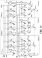
- FIG. 34 is a simplified circuit schematic illustrating another embodiment of a digital-input to analog current output multiplier (XD i I O ) that utilizes the meshed digital-to-analog multiplication (mD i S O ) method described in section 32 and section 32A.
- XD i I O digital-input to analog current output multiplier
- mD i S O meshed digital-to-analog multiplication
- FIG. 35 is a simplified circuit schematic illustrating another embodiment of a digital-input to analog current output multiplier (XD i I O ) that utilizes the meshed digital-to-analog multiplication (mD i S O ) method described in section 32.
- XD i I O digital-input to analog current output multiplier
- mD i S O meshed digital-to-analog multiplication
- FIG. 36 is a simplified block diagram illustrating a first non-linear digital-to-analog converter (NDAC) method.
- NDAC non-linear digital-to-analog converter
- FIG. 36A is a simplified block diagram illustrating a second non-linear digital-to-analog converter (NDAC) method, which utilizes the meshed digital-to-analog multiplication (mD i S O ) method that is discussed in section 32.
- NDAC non-linear digital-to-analog converter
- FIG. 37 is a simplified block diagram illustrating a third non-linear digital-to-analog converter (NDAC) method.
- NDAC non-linear digital-to-analog converter
- FIG. 38 is a simplified circuit schematic illustrating an embodiment of a non-linear digital-input to analog current output digital-to-analog converter (iNDAC 38 ), which utilizes the NDAC method described in section 37, wherein the non-linear output profile of iNDAC 38 is programmed to approximate a square transfer function.
- iNDAC 38 non-linear digital-input to analog current output digital-to-analog converter
- FIG. 39 is a simplified circuit schematic illustrating another embodiment of a non-linear digital-input to analog current output digital-to-analog converter (iNDAC 39 ), which utilizes the NDAC method described in section 36A wherein the non-linear output profile of iNDAC 39 is programmed to approximate a square transfer function.
- iNDAC 39 non-linear digital-input to analog current output digital-to-analog converter
- FIG. 40 is a simplified circuit schematic illustrating another embodiment of the digital-input to analog current output multiplier (XD i I O ) that utilizes the meshed digital-to-analog multiplication (mD i S O ) method described in the prior section 32, and wherein the XD i I O multiplier utilizes the multiple-channel data-converter method disclosed in section 19 when plurality of XD i I O multipliers are needed by an end-application.
- XD i I O digital-input to analog current output multiplier
- mD i S O meshed digital-to-analog multiplication
- FIG. 41 is a simplified circuit schematic illustrating another embodiment of the digital-input to analog current output multiplier (XD i I O ), which can be extended to plurality of XD i I O multipliers by sharing a central reference bias network (RBN) that bias the current reference network of each of the XD i I O multipliers.
- RNN central reference bias network
- FIG. 42 is a SPICE circuit simulations that illustrates the linearity error in % between an ideal output current (Io ideal ) of a XD i I O multiplier versus the simulated output current (Io simulation ) of a XD i I O multiplier that is arranged similar to that of FIG. 34 but having a 4-bit resolution.
- FIG. 43 is a SPICE circuit simulations that illustrates the linearity error in % between an ideal output current (Io ideal ) of a XD i I O multiplier versus the simulated output current (Io simulation ) of a XD i I O multiplier that is arranged similar to that of FIG. 40 but with a 6-bit resolution.
- FIG. 44 illustrates a SPICE simulations of a circuit comprising of an ideal square iDAC's output current (I X 2 ) plot versus the simulated output current (I O 2 ) plot of a square iDAC that is arranged similar to that of FIG. 38 but with a 7-bit resolution.
- FIG. 45 illustrates SPICE simulations of a circuit comprising of an ideal square iDAC's output current (I X 2 ) plot versus the simulated output current (I O 2 ) plot of a square iDAC that is arranged similar to that of FIG. 39 but with a 7-bit resolution.
- FIG. 46 illustrates SPICE simulations of a circuit comprising of an ideal XD i I O multiplier's output current (Io ideal ) plot versus the simulated output current (Io simulation ) plot of a XD i I O multiplier that is arranged similar to that of FIG. 41 but with a 7-bit resolution.
- FIG. 47 is a simplified block diagram illustrating an approximate non-linear digital data-converter method.
- FIG. 48 is a simplified block diagram illustrating an embodiment of a digital input to analog output multiplier (XD i I O ) that utilizes a time multiplexed digital squarer logic block.
- FIG. 49 is a simplified block diagram illustrating an embodiment of a digital input to analog output multiplier (XD i I O ) that utilizes a pair of digital squarer logic blocks.
- FIG. 50 is a simplified block diagram illustrating another embodiment of a digital input to analog output multiplier (XD i I O ) that utilizes a pair of digital squarer logic blocks.
- FIG. 51 is a simplified functional block diagram illustrating an embodiment of a mixed-signal current-mode multiply-accumulate (MACiDAC) circuit whose multiplication functions in accordance with the quarter square procedure, wherein the squarer logic block SQRL 51 is time multiplexed to perform a plurality of multiplications.
- MACiDAC mixed-signal current-mode multiply-accumulate
- FIG. 52 is a simplified functional block diagram illustrating an embodiment of a mixed-signal current-mode multiply-accumulate (MACiDAC) circuit that utilizes a digital-input to digital-output multiplier (MULTL 52 ).
- MACiDAC mixed-signal current-mode multiply-accumulate
- FIG. 53 illustrates SPICE simulations of a circuit equivalent to the MULTL 49 section of FIG. 49 , wherein the SQRLs 49 and SQRLd 49 blocks utilize the approximate (non-linear) square logic of aSQRL 47 disclosed in FIG. 47 .
- FIG. 54 illustrates a typical logic diagram of a 2-bit digital-input to 4-bit digital-output squarer (block SQR2t4 54 ).
- FIG. 55 illustrates a typical logic diagram of a 3-bit digital-input to 6-bit digital-output squarer (block SQR3t6 55 ).
- FIG. 56 illustrates a typical logic diagram of a 2-bit by 2-bit digital-input to 4-bit digital-output multiplier (block MULT2 ⁇ 2 56 ).
- FIG. 57 illustrates a block diagram of a squarer (SQR 57 ) that utilizes the segmented mixed mode multiplication.
- FIG. 58 illustrates a block diagram of an embodiment of a squarer (SQR 58 ) which is a segmented digital-input to current analog-output squarer utilizing meshed multipliers.
- FIG. 59 illustrates a block diagram of another embodiment of a squarer (SQR 59 ) which is a segmented digital-input to current analog-output squarer.
- FIG. 60 illustrates a block diagram of another embodiment of a squarer (SQR 60 ) which is a segmented digital-input to current analog-output squarer.
- FIG. 61 is a simplified block diagram (aSQR 61 ) illustrating an embodiment of a segmented digital-input to current analog-output approximate squarer.
- FIG. 62 illustrates a block diagram of an embodiment of a mixed-mode multiplier (sMULT 62 ) which is a segmented digital-input to current analog-output multiplier utilizing a time multiplexed digital multiplier.
- sMULT 62 mixed-mode multiplier
- FIG. 63 illustrates a block diagram of an embodiment of a mixed-mode multiply-accumulate (MAC 63 ).
- FIG. 64 is a simplified block diagram illustrating an embodiment a digital-input to current analog-output approximate square-accumulate (aSQRAC 64 ).
- FIG. 65 illustrates SPICE simulations of a circuit equivalent to the SQR 58 illustrated in FIG. 58 and disclosed in section 58.
- FIG. 66 illustrates SPICE simulations of a circuit equivalent to the aSQR 61 illustrated in FIG. 61 and disclosed in section 61.
- FIG. 67 illustrates SPICE simulations of a circuit equivalent to the SQR 59 illustrated in FIG. 59 and disclosed in section 59.
- FIG. 68 illustrates SPICE simulations of a circuit equivalent to the MULTL 62 described in section 62 and illustrated in FIG. 62 .
- FIG. 69 is a simplified circuit schematic illustrating an embodiment of SRAM based Compute-In-Memory (CIM) utilizing a meshed multiplier (XD I I O ) and reference bias network (RBN).
- CIM Compute-In-Memory
- FIG. 70 is a simplified circuit schematic illustrating another embodiment of SRAM based Compute-In-Memory (CIM) utilizing a current-mode Multiply-Accumulate (iMAC) system comprising a plurality of meshed multiplier (XD I I O ) with a bias current-mode Digital-to-Analog-Converter (iDAC), and a current-mode Analog-To-Digital-Converter (iADC).
- CIM Compute-In-Memory
- iMAC current-mode Multiply-Accumulate
- An aspect of the present disclosure is a floating current-mode digital-to-analog converter (iDAC) method in an integrated circuit, the floating iDAC method comprising: programming a plurality of voltage-controlled-current sources (VCCS) to generate a plurality of current signals to be at least one of equally weighted currents, binarily weighted currents, non-linear weighted currents, and individually weighted currents; summing the plurality of current signals to create a summation current signal (S SUM ) at a reference current input port (A R ); wherein the floating iDAC has a digital input word (D i ) that controls a plurality of current switches (iSW) that respectively steer the plurality of current signals to at least one of a positive current output port (I O + ), and a negative current output port (I O ⁇ ) of the floating iDAC; wherein the currents flowing through the I O + port and the I O ⁇ port are proportional to the current signal flowing through the A R port, and
- the floating iDAC method further comprising: receiving current signals from respective I O + ports and I O ⁇ ports, of at least one of a subsequent iDAC, into the respective at least one of the I O + port, and the I O ⁇ port of the floating iDAC; wherein the A R port receives a reference current signal (S R ); wherein the reference input signal of each of the subsequent iDACs is proportional to the S R signal; and wherein the at least one of the subsequent iDACs effectively increases the resolution of the floating iDAC.
- S R reference current signal
- the floating iDAC method further comprising: receiving the current signal from a first iDAC into a reference input port of a second iDAC, wherein at least one of the first iDAC and the second iDAC is the floating iDAC; generating a multiplication output current signal (S MULT ) at an output port of the second iDAC; and wherein the S MULT signal is proportional to the S R signal and responsive to the product of a digital input word of the first iDAC and, a digital input word of the second iDAC.
- S MULT multiplication output current signal
- the floating iDAC method further comprising: generating a plurality of S MULT signals; and combining the plurality of S MULT signals to generate a multiply-accumulate current signal (S MAC ), wherein the S MAC signal is a summation of the plurality of the S MULT signals.
- S MAC multiply-accumulate current signal
- the floating iDAC method further comprising: combining the S MAC signal with a bias current signal (S B ) from a bias current iDAC to generate a biased multiply-accumulate current signal (S BMAC ), wherein the S BMAC signal is the summation of the S MAC signal and the S B signal.
- the floating iDAC method further comprising: digitizing the S BMAC signal in a current-mode analog-to-digital converter (iADC).
- the floating iDAC method further comprising: combining a plurality of S BMAC signals, wherein the combining the plurality of S BMAC signals forms a current-mode artificial neural network (iANN).
- iANN current-mode artificial neural network
- the floating iDAC method further comprising: receiving currents from I O + port and I O ⁇ port, of a plurality of subsequent floating iDACs, into the respective I O + port and the I O ⁇ port of the floating iDAC to generate an I Op + and an I Op ⁇ ; generating a plurality of reference current sources (S R )s to be at least one of equally weighted currents, binarily weighted currents, non-linear weighted currents, and individually weighted currents; receiving each of the plurality of S R signals respectively into the I sR port of each subsequent floating iDAC; receiving a X digital word of width m, and a Y digital word of width n, wherein each bit weight of the X word of width m corresponds to the respective weight of each of the plurality of reference currents corresponding respectively to each of the floating iDACs, and wherein each bit weight of the
- a floating current-mode digital-to-analog converter (iDAC) method in an integrated circuit comprising: generating a plurality of currents in a plurality of metal-oxide-semiconductor-field-effect-transistors (MOSFETs), wherein a weighting relationship among each of the plurality of currents in the MOSFETs is at least one of equally weighted, binarily weighted, non-linear weighted, and individually weighted; steering each of the plurality of current signals in the plurality of MOSFETs respectively through each input terminal of a plurality of current switches (iSW); steering each of the plurality of current signals through the plurality of iSWs respectively to each output terminal of the plurality of current switches (iSW) to at least one of a positive current output port (I O + ), and a negative current output port (I O ⁇ ); receiving a digital input word (D i ), and respectively controlling the steering of each of the plurality of the plurality of current switches (I O +
- the floating iDAC method further comprising: receiving into the at least one of the I O + port, and the I O ⁇ port of the floating iDAC, currents from respective I O + ports and I O ⁇ ports from at least one of a subsequent iDAC, wherein the at least one of the subsequent iDAC effectively increases the resolution of the floating iDAC.
- the floating iDAC method further comprising: receiving the output current signal from a first iDAC into a reference input port of a second iDAC, wherein at least one of the first iDAC and the second iDAC is the floating iDAC; and generating a multiplication output current signal (S MULT ) at an output of the second iDAC.
- S MULT multiplication output current signal
- the floating iDAC method further comprising: generating a plurality of S MULT signals; and combining the plurality of S MULT signals to generate a multiply-accumulate current signal (S MAC ), wherein the S MAC signal is a summation of the plurality of the S MULT signals.
- S MAC multiply-accumulate current signal
- the floating iDAC method further comprising: generating a bias current signal (S B ) by an iDAC; and combining the S MAC signal with the S B signal to generate a biased multiply-accumulate current signal (S BMAC ), wherein the S BMAC signal is a summation of the S MAC signal and the S B signal.
- the floating iDAC method further comprising: digitizing the S BMAC signal in a current-mode analog-to-digital converter (iADC).
- the floating iDAC method further comprising: combining a plurality of S BMAC signals, wherein the combining the plurality of S BMAC signals forms a current-mode artificial neural network (iANN).
- iANN current-mode artificial neural network
- Another aspect of the present disclosure is a mixed-signal current-mode multiply-accumulate (iMAC) method in integrated circuits, the mixed-signal iMAC method comprising: generating a plurality of first current output signals (S 1 O )s by a plurality of first current-mode digital-to-analog converters (iDAC 1 )s; receiving the plurality of S 1 O signals into a respective plurality of reference input ports (A 2 R ) of a plurality of second current-mode digital-to-analog-converters (iDAC 2 )s; generating a plurality of multiplication output current signals (S MULT )s at the plurality of A 2 R ports; combining a plurality of S MULT signals together to generate a multiply-accumulate current signal (S MAC ); and wherein the S MAC signal is a summation of a plurality of second current output signals (S 2 O )s of the plurality of iDAC 2 s .
- the mixed-signal iMAC method further comprising: generating a bias current signal (S B ) by a bias iDAC; and combining the S MAC signal with the S B signal to generate a biased multiply-accumulate current signal (S BMAC ), wherein the S BMAC signal is a summation of the S MAC signal and the S B signal.
- the mixed-signal iMAC method further comprising: digitizing the S BMAC signal in a current-mode analog-to-digital converter (iADC).
- the mixed-signal iMAC method further comprising: combining a plurality of S BMAC signals, wherein the combining the plurality of S BMAC signals forms a current-mode artificial neural network (iANN).
- iANN current-mode artificial neural network
- Another aspect of the present disclosure is a factorized current-mode digital-to-analog converter (iDAC) method in an integrated circuit, the factorized iDAC method comprising: generating a scaled top output current signal (A t F t ) as a product of a top scale factor (F t ) and a top output current signal (A t ) of a top iDAC (iDAC t ), wherein the iDAC t receives a top digital word (D t ) that is t-bits wide, and wherein the iDAC t receives a top reference current signal (t R ), and wherein the iDAC t is binary weighted and wherein F t and t are each between zero and eight; generating a scaled middle output current signal (A m F m ) as a product of a middle scale factor (F m ) and a middle output current signal (A m ) of a middle iDAC (iDAC t ), wherein the iDAC
- a factorized current-mode digital-to-analog converter (iDAC) method in an integrated circuit comprising: generating a scaled top output current signal (A t F t ) as a product of a top scale factor (F t ) and a top output current signal (A t ) of a top iDAC (iDAC t ), wherein the iDAC t receives a top digital word (D t ) that is t-bits wide, and wherein the iDAC t receives a top reference current signal (t R ), and wherein iDAC t is binary weighted, and wherein F t and t are each between zero and eight; generating a scaled middle output current signal (A m F m ) as a product of a middle scale factor (F m ) and a middle output current signal (A m ) of a middle iDAC (iDAC t ), wherein the iDAC
- the factorized iDAC method further comprising: receiving the output current signal from a first iDAC into a reference input port of a second iDAC, wherein at least one of the first iDAC and the second iDAC is the factorized iDAC; generating a multiplication output current signal (S MULT ) at an output port of the second iDAC; and wherein the S MULT signal is proportional to the S R signal and responsive to the product of digital input words of the first iDAC and the second iDAC.
- S MULT multiplication output current signal
- the factorized iDAC method further comprising: generating a plurality of S MULT signals; and combining the plurality of S MULT signals to generate a multiply-accumulate current signal (S MAC ), wherein the S MAC signal is a summation of the plurality of the S MULT signals.
- S MAC multiply-accumulate current signal
- the factorized iDAC method further comprising: generating a bias current signal (S B ) by a bias iDAC; and combining the S MAC signal with the S B signal to generate a biased multiply-accumulate current signal (S BMAC ), wherein the S BMAC signal is a summation of the S MAC signal and the S B signal.
- the factorized iDAC method further comprising: digitizing the S BMAC signal in a current-mode analog-to-digital converter (iADC).
- the factorized iDAC method further comprising: combining a plurality of S BMAC signals, wherein the combining the plurality of S BMAC signals forms a current-mode artificial neural network (iANN).
- iANN current-mode artificial neural network
- Another aspect of the present disclosure is a mixed-signal scalar current-mode multiply-accumulate (iMAC) method in an integrated circuit, the mixed-signal scalar iMAC method comprising: generating a scalar current (S S ) by a first current-mode DAC (iDAC); replicating the S S signal to generate a plurality of scalar current replica signals (S S D); receiving the plurality of S SD signals respectively into a reference input of each of a plurality of second iDACs; and generating a plurality of current output Signals (S o )s of the plurality of the second iDACs; combining the plurality of S o signals of the plurality of second iDACs to generate a multiply-accumulate current (S MAC ); and wherein the S MAC is a summation of the respective plurality of S o signals.
- S S scalar current
- iDAC current-mode multiply-accumulate
- the mixed-signal scalar iMAC method further comprising: combining the S MAC signal with a bias current signal (S B ) from a bias current iDAC to generate a biased multiply-accumulate current signal (S BMAC ), wherein the S BMAC signal is the summation of the S MAC signal and the S B signal.
- the mixed-signal scalar iMAC method further comprising: digitizing the S BMAC signal in a current-mode analog-to-digital converter (iADC).
- the mixed-signal scalar iMAC method further comprising: combining a plurality of S BMAC signals, wherein the combining the plurality of S BMAC signals forms a current-mode artificial neural network (iANN).
- iANN current-mode artificial neural network
- Another aspect of the present disclosure is a mixed-signal scalar current-mode multiply-accumulate (iMAC) method in an integrated circuit, the mixed-signal scalar iMAC method comprising: receiving a first and subsequent reference current signals, each respectively to a reference port (A R ) of each of first current mode iDAC of a plurality of first current mode iDACs; generating a plurality of output current signals (S O )s by the plurality of first current-mode DACs (iDAC); combining the plurality of S O signals of the plurality of first iDACs to generate a current signal (S Osum ), wherein the S Osum is a summation of the plurality of S O signals; mirroring the S Osum signal to create a mirrored S Osum signal, S Osumm ; receiving the S Osumm signal into a reference input port of a scalar iDAC; and generating a multiply-accumulate current signal (S MAC ) at the output port of the scalar
- the mixed-signal scalar iMAC method further comprising: combining the S MAC signal with a bias current signal (S B ) from a bias current iDAC to generate a biased multiply-accumulate current signal (S BMAC ), wherein the S BMAC signal is the summation of the S MAC signal and the S B signal.
- the mixed-signal scalar current-mode multiply-accumulate (iMAC) method in an integrated circuit, the mixed-signal scalar iMAC method further comprising: digitizing the S BMAC signal in a current-mode analog-to-digital converter (iADC).
- the mixed-signal scalar iMAC method further comprising: combining a plurality of S BMAC signals, wherein the combining the plurality of S BMAC signals forms a current-mode artificial neural network (iANN).
- iANN current-mode artificial neural network
- NDAC non-linear digital-to-analog conversion
- the method comprising: generating a non-linear Most-Significant-Portion (MSP) analog output signal (So MPS N ) that is proportional to a MSP reference signal (Sr MSP ), and is responsive to a bank of Most-Significant-Bits (MSBs) of a digital input word (Di MSP ); generating a linear Least-Significant-Portion (LSP) analog output signal (So LSP L ) that is proportional to a LSP reference signal (Sr LSP ), and is responsive to a bank of Least-Significant-Bits (LSBs) of a digital word (Di LSP ), and is responsive to the Di MSP word; combining the So MPS N signal and the So LSP L signal to generate a non-linear analog output signal (So N ) that is proportional to a reference signal (MSP)
- MSP MSP reference signal
- non-linear digital-to-analog conversion (NDAC) method in an integrated circuit, the method further comprising: wherein the So MPS N signal is generated by a non-linear MSP digital-to-analog converter (DAC MSP N ) having a reference network comprised of a sequence of scaled MSP reference signals (Sr MSP n ); and wherein the sequence of scaled Sr MSP N signals are at least one of squarely weighted, logarithmically weighted, non-linearly weighted, and individually weighted.
- DAC MSP N non-linear MSP digital-to-analog converter
- NDAC non-linear digital-to-analog conversion
- the method further comprising: generating the So LSP L signal by a plurality of linear LSP Digital-to-Analog Converters (DAC LSP L )s comprised of a first linear LSP DAC (DAC 1 LSP L ), and a second linear LSP DAC (DAC 2 LSP L ); generating an output signal (So 1 LSP L ) by the DAC 1 LSP L that is proportional to a first LSP reference signal (Sr 1 LSP ), and is responsive to the Di MSP word; combining the So 1 LSP L signal with a reference offset signal (Sr OFS ) to generate a second reference signal (Sr 2 LSP L ); receiving the Sr 2 LSP signal into a reference input port (Ar 2 LSP 2 ) of the DAC 2 LSP 2 ; and generating the So LSP L signal at an output port (Ao 2 LSP L ) of the DAC 2 LSP L
- NDAC non-linear digital-to-analog conversion
- the method further comprising: multiplying the Di LSP word and the Di MSP word to generate a multiplication digital word (Di LSP ⁇ Di MSP ); generating an output signal (So 1 LSP L ) by a first LSP Digital-to-Analog Converter (DAC 1 LSP L ), wherein the So 1 LSP L signal is proportional to a first LSP reference signal (Sr 1 LSP ), and is responsive to the Di LSP ⁇ Di MSP word; generating an output offset signal (Sfo LSP L ) by a second LSP Digital-to-Analog-Converter (DAC 2 LSP L ), wherein Sfo LSP L signal is proportional to a second LSP reference signal (Sr 2 LSP ), and is responsive to the Di LSP word; and combining the So 1 LSP L signal and the Sfo LSP L signal to generate the So LSP L signal.
- DAC 1 L LSP Digital-to
- NDAC non-linear digital-to-analog conversion
- the method further comprising: receiving the Di LSP word and the Di MSP word into a linearly meshed digital-input to analog-output multiplier (mDiSo LSP L ) to generate an output signal (So 1 LSP L ) that is proportional to a first LSP reference signal (Sr 1 LSP ); generating an output offset signal (Sfo LSP L ) by a second LSP Digital-to-Analog-Converter (DAC 2 LSP L ) that is proportional to a second LSP reference signal (Sr 2 LSP ), and is responsive to the Di LSP word; and combining So 1 LSP L signal and the Sfo LSP L signal to generated the So LSP L signal.
- mDiSo LSP L linearly meshed digital-input to analog-output multiplier
- non-linear digital-to-analog conversion (NDAC) method in an integrated circuit, the method further comprising: generating at least one So MPS N by at least one non-linear MSP Digital-to-Analog Converter (DAC MSP N ); generating at least one So LPS L by at least one linear LSP Digital-to-Analog Converter (DAC LSP L ); generating at least one So N signal that is proportional to the reference signal (S R ), wherein the at least one So N signal is responsive to at least one D i word; wherein the reference network of each of the DAC MSP L is comprised of a sequence of non-linearly scaled MSP reference signals (Sr MSP L ) that are proportional to the Sr MSP signal; wherein the reference network of each of the DAC LSP L is comprised of a sequence of scaled LSP reference signals (Sr LSP L ) that are proportional to the Sr LSP signal; wherein each of the sequence of Sr MSP N signals is
- non-linear digital-to-analog conversion (NDAC) method in an integrated circuit, the method further comprising: wherein a plurality of the at least one So N signal has a square profile; wherein a p-channel So N signal, of the plurality of So N signals, is responsive to a p-channel D word; wherein a q-channel So N signal, of the plurality of So N signals, is responsive to a q-channel D word; wherein the p-channel So N and the q-channel So N signals are subtracted from one another to generate a scaled So xy signal; wherein the p-channel D word is comprised of a scaled X digital word and a scaled Y digital word that are added to one another; wherein the q-channel D word is comprised of a scaled Y digital word and a scaled Y digital word that are subtracted from one another; and wherein the scaled So xy signal is proportional to the S R , and is an analog representation of
- NDAC non-linear digital-to-analog converter
- the system comprising: a first non-linear Digital-to-Analog-Converter (DAC QM ), the DAC QM comprising a digital input port (D QM ), an analog output port (Ao QM ), and an analog reference input port (Ar QM ); a first linear Digital-to-Analog-Converter (DAC 1L ), the DAC 1L having a digital input port (D 1L ), an analog output port (Ao 1L ), and an analog reference input port (Ar 1L ); a second linear Digital-to-Analog-Converter (DAC 2L ), the DAC 2L having a digital input port (D 2L ), an analog output port (Ao 2L ), and an analog reference input port (Ar 2L ); a digital input word (D) comprised of a Most-Significant-Bits (MSB)
- MSB Most-Significant-Bits
- non-linear digital-to-analog converter (NDAC) system in an integrated circuit, the system further comprising: wherein the sequence of Sr MSP N signals, and the sequence of Sr LSP signals, are biased from a common reference bias network (RBN).
- RNN common reference bias network
- non-linear digital-to-analog converter (NDAC) system in an integrated circuit, the system further comprising: a plurality of So N signals having a square profile; wherein a p-channel So N signal, of the plurality of So N signals, is responsive to a p-channel D word; wherein a q-channel So N signal, of the plurality of So N signals, is responsive to a q-channel D word; wherein the p-channel So N and the q-channel So N signals are subtracted from one another to generate a scaled So xy signal; wherein the p-channel D word is comprised of a scaled X digital word and a scaled Y digital word that are added to one another; wherein the q-channel D word is comprised of a scaled Y digital word and a scaled Y digital word that are subtracted from one another; and wherein the scaled So xy signal is proportional to the S R , and is an analog representation of a scaled multiplication
- NDAC non-linear digital-to-analog converter
- NDAC non-linear digital-to-analog converter
- DAC QM non-linear digital-to-analog-converter
- D QM digital input port
- Ao QM analog output port
- Ar QM analog reference input port
- DAC 1L first linear digital-to-analog-converter
- DAC 2L second linear digital-to-analog-converter
- D 2L digital input port
- Ao 2L analog output port
- Ar 2L analog reference input port
- NDAC non-linear digital-to-analog converter
- non-linear digital-to-analog converter (NDAC) system in an integrated circuit, the system further comprising a plurality of So N signals having a square profile; wherein a p-channel So N signal, of the plurality of So N signals, is responsive to a p-channel D word; wherein a q-channel So N signal, of the plurality of So N signals, is responsive to a q-channel D word; wherein the p-channel So N and the q-channel So N signals are subtracted from one another to generate a scaled So xy signal; wherein the p-channel D word is comprised of a scaled X digital word and a scaled Y digital word that are added to one another; wherein the q-channel D word is comprised of a scaled Y digital word and a scaled Y digital word that are subtracted from one another; and wherein the scaled So xy signal is proportional to the S R and is an analog representation of a scaled multiplication product of the
- NDAC non-linear digital-to-analog converter
- NDAC non-linear digital-to-analog converter
- the system comprising: a first non-linear Digital-to-Analog-Converter (DAC QM ), the DAC QM having a digital input port (D QM ), an analog output port (Ao QM ), and an analog reference input port (Ar QM ); a first linear Digital-to-Analog-Converter (DAC 1L ), the DAC 1L having a digital input port (D 1L ), an analog output port (Ao 1L ), and an analog reference input port (Ar 1L ); a linearly meshed digital-input to analog-output multiplier (mDiSo LSP L ), the mDiSo LSP L having an M digital input port (M) and a N digital port (N), an analog output port (Ao 2L ), and an analog reference input port (Ar 2L ); a digital input word (D) comprised of
- NDAC non-linear digital-to-analog converter
- non-linear digital-to-analog converter (NDAC) system in an integrated circuit, the system further comprising: a plurality of So N signals having a square profile; wherein a p-channel So N signal, of the plurality of So N signals, is responsive to a p-channel D word; wherein a q-channel So N signal, of the plurality of So N signals, is responsive to a q-channel D word; wherein the p-channel So N and the q-channel So N signals are subtracted from one another to generate a scaled So xy signal; wherein the p-channel D word is comprised of a scaled X digital word and a scaled Y digital word that are added to one another; wherein the q-channel D word is comprised of a scaled Y digital word and a scaled Y digital word that are subtracted from one another; and wherein the scaled So xy signal is proportional to the S R , and is an analog representation of a scaled multiplication
- NDAC non-linear digital-to-analog converter
- Another aspect of the present disclosure is a multiple channel current-mode data converter method in an integrated circuit, the method comprising: generating a sequence of reference bias current signals (Si Rb ) from a reference bias network (RBN); mirroring the sequence of Si Rb signals from the RBN into at least one iDC; wherein the scaling of the mirroring of the sequence of Si Rb signals from the RBN into at least one iDC, is individually scaled; wherein the sequence of Si Rb signals from the RBN is weighted at least equally, binarily, non-linearly, and individually; wherein each Si Rb signal from the sequence of Si Rb signals from the RBN is scaled proportionately to a reference current signal (S R ); wherein each Si Rb signal from the sequence of Si Rb signals from the RBN is mirrored from the S R signal; wherein the sequence of Si Rb signals, from the RBN in the at least one iDC, program the reference current network of the at least one iDC, which establishes the input-to-output
- the method further comprising: regulating the S R signal from the RBN; wherein the analog ports of the at least one iDC substantially track power supply voltage variations; and wherein if the at least one iDC includes an iDAC, then the analog output current signal of each iDAC is substantially desensitized with respect to power supply variations; and wherein if the at least one iDC includes an iADC, then a digital output word of each iADC is substantially desensitized with respect to power supply variations.
- the method further comprising: wherein at least one of S R , S Y , S X , and S O signals are generated without cascode. Further aspects of the multiple channel current-mode data converter method in an integrated circuit, the method further comprising: wherein the respective voltages at A mR and A mY ports track power supply voltage variations in substantial proportion to one another; wherein the respective voltages at A mX and A mO ports track power supply voltage variations in substantial proportion to one another; and wherein the at least one S O signal of the at least one iMULT is substantially insensitive to power supply voltage variations.
- the method further comprising: wherein if the at least one iDC includes an iDAC: wherein the sequence of Si Rb signals from the RBN is weighted squarely; summing at least one pair of digital input words (D x and D y ) together to generate at least a scaled D x+y digital word; subtracting the at least one pair of digital input words D x and D y from one another to generate at least one scaled D x ⁇ y digital word; receiving at least one pair of scaled digital input words (D x+y and D x ⁇ y ) respectively into each of at least one pair of iDACs (iDAC (x+y) 2 and iDAC (x ⁇ y) 2 ); generating at least one pair of current output signals (S (x+y) 2 and S (x ⁇ y) 2 ) that are proportional to the S R , and responsive to the at least one pair of the scaled D x+y and D x ⁇ y words
- the method further comprising: wherein if the at least one iDC includes an iDAC: wherein the sequence of Si Rb signals from the RBN is weighted logarithmically; receiving at least one pair of digital input words (D X and D Y ) respectively into at least one pair of the iDACs (iDAC log X , and iDAC log Y ); generating at least one pair of current output signals (S log X and S log Y ) that are proportional to the S R signal, and responsive to the at least one pair of D X and D Y words; and summing the S log Y and S log Y signals to generate at least one multiplication output current (S log MULT ), wherein S log MULT is the analog representation of a digital logarithmic word (log D x ⁇ D y ).
- a power supply desensitization method in a current-mode digital-to-analog converter (iDAC) in an integrated circuit comprising: receiving a digital input word (D X ) into a x-channel iDAC (iDAC X ) having an analog output current signal (S X ), and a reference input signal (S RX ), wherein the iDAC X is without cascodes; receiving a digital input word (D Y ) into a y-channel iDAC (iDAC Y ) having an analog output current signal (S Y ), and a reference input signal (S RY ), wherein the iDAC Y is without cascodes; receiving the S X signal into an input port of a power supply desensitization (PSR) circuit; regulating and generating the S RY reference input signal at an output port of the PSR circuit, wherein the S Y signal is desensitized from power supply variations; and generating a multiplication output current (PSR)
- MOSFET Metal-Oxide-Semiconductor-Field-Effect-Transistors
- W/L Scalable/L
- iDC current-mode Data-Converter
- Another aspect of the present disclosure is a multiple channel current-mode data converter system in an integrated circuit, the system comprising: a sequence of current mirrors (iCM), each iCM having a current mirror input port (Ai iCM ) for receiving a sequence of scaled reference current signals S R , a current mirror output port (Ao iCM ), and an input-to-output gain factor (G iCM ); a current mode data converter (iDC) having a sequence of reference input ports (Ar iDC ); the Ao iCM port of each of the sequence of iCMs coupled to the respective Ar iDC port of the sequence of Ar iDC ports of the iDC; wherein each scaled reference current S R of a sequence of scaled S R signals is coupled respectively to the Ai iCM port of each iCM of the sequence of iCMs; wherein the G iCM of each iCM of the sequence of iCM is programmed individually; wherein the iDC is at least one of current-mode Digital-
- Another aspect of the present disclosure is a multiple channel current-mode data converter system in an integrated circuit, the system comprising: a sequence of current mirrors (iCM), each iCM having a current mirror input port (Ai iCM ) for receiving a sequence of scaled reference current signals (S R )s, a current mirror output port (Ao iCM ), and an input-to-output gain factor (G iCM ); one or more current mode data converters (iDC), each of the one or more iDCs having a sequence of reference input ports (Ar iDC ); each of the one or more Ao iCM ports of each iCM of the sequence of iCMs respectively coupled to the Ar iDC port of the sequence of Ar DC ports of the one or more iDCs; wherein each scaled S R signal of a sequence of scaled S R signals is coupled respectively to the Ai iCM port of each iCM of the sequence of iCMs; wherein the G iCM of each iCM of the sequence of
- Another aspect of the present disclosure is a multiple channel current-mode data converter system in an integrated circuit, the system comprising: a sequence of Current-Controlled-Voltage-Sources (CCVS)s, each CCVS in the sequence of the CCVSs having an input current port (Ai ccvs ) for receiving a sequence of scaled reference current signals (S R )s, an output port (Ao ccvs ) for providing an output voltage signal (So ccvs ), and an input-current to output-voltage gain factor (G ccvs ); a plurality of current mode data converters (iDC); each iDC of the plurality of iDCs having a sequence of Voltage-Controlled-Current-Sources (VCCS)s; each VCCS of the sequence of VCCSs, in each iDC of the plurality of iDCs, having an input voltage port (Ai vccs ), an output current port (Ao vccs ) for providing an output current
- Another aspect of the present disclosure is a multiple channel current-mode data converter method in an integrated circuit, the method comprising: generating a sequence of reference bias current signals (Si Rb ); receiving the sequence of Si Rb signals into a sequence of Current-Controlled-Voltage-Sources (CCVS)s to generate a sequence of reference bias voltage signals (Sv Rb ); receiving the sequence of Sv Rb signals into at least one sequence of Voltage-Controlled-Current-Sources (VCCS)s in at least one current mode data converter (iDC), wherein the at least one sequence of VCCSs replicates the sequence of Si Rb signals; wherein the sequence of Si Rb signals is weighted at least one of equally, binarily, non-linearly, and individually, and wherein each S Rb signal is scaled proportionately to a reference current signal (S R ); wherein the sequence of VCCS in the at least one iDC arranges the reference current network of each respective iDC which establishes the input-to-output transfer function of
- a meshed multiplier system in an integrated circuit, the system comprising: a first digital input port having a of width of M bits of a first digital input word D X ; a second digital input port having a width of N bits of a second digital input word D Y ; a plurality of N scaled current source banks, each scaled current source bank uniquely corresponding to a bit of D Y ; each of the N scaled current source banks comprising a plurality of M scaled current sources, each scaled current source having a corresponding first switch and a corresponding second switch, each current source uniquely corresponding to a bit of the first digital input word D X ; each scaled current source in each scaled current source bank coupled to an input of its corresponding first switch, the first switch responsive to the bit of the first digital input word DX corresponding to the scaled current source; the first switch having an output coupled to an input of its corresponding second switch, the second switch responsive to the bit of the second digital input word D Y corresponding to the scaled
- Another aspect of the present disclosure is a meshed multiplier method in an integrated circuit, the method comprising: receiving a first digital input word DX of width of M bits, wherein M is less than 17; receiving a second digital input word D Y of width of N bits, wherein N is less than 17; activating one bank of N banks of M scaled current sources responsive to a bit of D Y corresponding to the one bank of N banks, thereby activating each of the M scaled current sources; receiving current into an output node from one of the activated M scaled current sources responsive to a corresponding bit of D X .
- Further aspects of the meshed multiplier system in an integrated circuit the system further comprising: wherein M and N are equal.
- a meshed digital-input to analog current-output multiplier system in an integrated circuit, the system comprising: a digital-input to analog-output multiplier (XD i I o ) comprised of a Ao XY port, a first digital input port (D X ) wherein the DX port is M-bit wide, a second digital input port (D Y ) wherein the D Y port is N-bit wide, and a reference port for receiving a S Ru signal;
- the XD i I o comprising: a sequence of M meshed digital-input to analog current-output sub-multipliers (mD i I o ), wherein each mD i I o is comprised of a first switch bank (iSW 1 B ), a second switch bank (iSW 2 B ), a current reference signals bank (S R B ), and a first digital 1-bit wide port (B M ); for each mD i I o , each i
- each S R B signal bank comprised of a sequence of N current reference signal ports (A R ) for receiving sequence of N scaled current reference signals (S R ), wherein the sequence of N scaled S R signals is at least one of binarily weighted, linearly weighted, and individually weighted, and wherein each scaled S R signal is proportional to the S Ru signal; for each mD i I o , the sequence of N scaled S R sources of the S R B signal banks coupled respectively to the sequence of N input ports of the iSW 1 B switch bank; for each mD i I o , the sequence of N output ports of the iSW 2 B switch bank coupled to the Ao XY port; for each mD i I o , the sequence of M
- the system further comprising: a plurality of the XD i I o ; the Ao XY port from each of the plurality of XD i I o s coupled to an Ao MAC port; wherein a signal through the Ao MAC port is a multiply-accumulate current signal (So MAC ), wherein the So MAC signal is a summation of signals through the plurality of Ao XY ports; and wherein the So MAC is proportional to the S Ru source and responsive to a plurality of digital words that are the multiplication product of pairs of digital words inputted to a plurality of pairs of D X and D Y ports.
- So MAC multiply-accumulate current signal
- the system further comprising: a bias current-mode Digital-to-Analog-Converter (iDAC) for generating a bias current signal (S B ), the bias current signal (S B ) coupled to the So MAC signal to generate a biased multiply-accumulate current signal (So BMAC ), wherein the So BMAC signal is the summation of the So MAC signal and the S B signal.
- iDAC Digital-to-Analog-Converter
- a current-mode Analog-to-Digital Converter for digitizing the So BMAC signal to generate a Do BMAC word that is a digital representation of the So BMAC signal.
- iADC current-mode Analog-to-Digital Converter
- each scaled S R source of the sequence of N scaled S R sources of each of the S R B signal bank of each mD i I o , is biased from a common reference bias network (RBN).
- MOSFET Metal-Oxide-Semiconductor-Field-Effect-Transistors
- a meshed digital-input to analog current-output multiplier system in an integrated circuit, the system comprising: a digital-input to analog-output multiplier (XD i I o ) comprised of a Ao XY port, a first digital input port (D X ) wherein the D X port is w-bit wide, a second digital input port (D Y ) wherein the D Y port is z-bit wide, and a reference input port for receiving a S Ru signal;
- the XD i I o comprising: a plurality of Metal-Oxide-Semiconductor-Field-Effect-Transistors (MOSFET)s, each having a gate-port, a drain-port, and a source port, and each having a scale (W/L); a sequence of M meshed digital-input to analog current-output sub-multipliers (mD i I o ), wherein each mD i I I
- aNDC approximate non-linear digital data-conversion
- Z an at least one input digital word (Z) comprised of an at least one Most-Significant-Bits (MSB) portion digital word (Z MSP ) and an at least one Least-Significant-Bits (LSB) portion digital word (Z LSP ); generating an at least one square digital word (Z MPS 2 ) from the at least one Z MSP digital word, wherein the relationship between the at least one Z MSP digital word and the at least one Z MPS 2 digital word follows a square profile; multiplying the at least one Z LSP digital word and the at least one Z MSP digital words to generate an at least one multiplication digital word (Z MSP ⁇ Z LSP ); scaling the at least one Z MSP ⁇ Z LSP digital word by an at least one first binary scale factor (S L ) to generate an at least one scaled multiplication digital word (S L ⁇ Z MSP ⁇ Z
- aNDC approximate non-linear digital data-conversion
- aNDC approximate non-linear digital data-conversion
- aNDC approximate non-linear digital data-conversion
- aNDC approximate non-linear digital data-conversion
- the method further comprising: generating an at least one plurality of approximate ⁇ 4x′ ⁇ y′ analog signals; generating an at least one approximate multiply-accumulate analog signal ( ⁇ 4x′ ⁇ y′) by combining the at least one plurality of approximate ⁇ 4x′ ⁇ y′ analog signals; generating an at least one offset analog signal (b′) by inputting an at least one offset digital word (B) onto an at least one offset Digital-to-Analog Converter (DAC OFS ); generating an at least one offsetting approximate ⁇ 4x′ ⁇ y′ analog signal ( ⁇ 4x′ ⁇ y′+b′) by combining the at least one approximate ⁇ 4x′ ⁇ y′ analog signal with the at least one b′ analog signal; and generating an at least one offsetting approximate multiply-accumulate digital word ( ⁇ 4X ⁇ Y+B) by inputting the at least one approximate ⁇ 4x′ ⁇ y′+b′ analog signal onto an at
- Another aspect of the present disclosure is a current mode multiply accumulate method in an integrated circuit, the method comprising: multiplying an at least one X digital word by an at least one Y digital word to generate an at least one multiplication digital word (X ⁇ Y); inputting the at least one X ⁇ Y digital word onto an at least one current-mode Digital-Analog-Converter to generate an at least one multiplication analog current signal (x′ ⁇ y′); generating an at least one offset analog current signal (b′) by inputting an at least one offset digital word (B) onto an at least one offset current-mode Digital-to-Analog Converter (DAC OFS ); generating an at least one offsetting multiply-accumulate current signal (S iMAC ) by summing the at least one x′ ⁇ y′ analog current signal with the at least one b′ analog current signal; and generating an at least one offsetting multiply-accumulate digital word (Sd MAC ) by inputting the at least one S iMAC analog signal onto an at least one current-mode Analog-to
- the method further comprising: wherein multiplying the at least one X digital word by the at least one Y digital word to generate the at least one multiplication digital word (X ⁇ Y) further comprises; summing the at least one X and the at least one Y digital words to generate an at least one X+Y digital word (Z s ); subtracting the at least one Y and from the at least one X digital words to generate an at least one X ⁇ Y digital word (Z d ); generating an at least one summing absolute value digital word
- digital word is the absolute value of the at least one Z s digital word; generating an at least one deducting absolute value digital word
- digital word is the absolute value of the at least one Z d digital word; generating an at least one summing square digital word (
- the method further comprising: wherein generating at least one of the at least one summing square digital word
- Another aspect of the present disclosure is a segmented squaring method in an integrated circuit, the method comprising: wherein an at least one input signal (Z) further comprising of an at least one Most-Significant-Portion (MSP) signal (Z MSP ) and an at least one Least-Significant-Portion signal (Z MSP ); generating an at least one MSP squared signal (Z MPS 2 ) by squaring the at least one Z MSP signal; generating an at least one LSP squared signal (Z LPS 2 ) by squaring the at least one Z LSP signal; and generating an at least one LSP and MSP cross-multiplication signal (Z LSP ⁇ Z MSP ) by multiplying the at least one Z LSP signal with the at least one Z MSP signal.
- Z an at least one input signal
- Z MSP Most-Significant-Portion
- Z MSP Least-Significant-Portion signal
- the method further comprising: scaling the at least one Z MPS 2 signal by an at least one top-scale-factor (s T ) to generate an at least one s T ⁇ Z MPS 2 signal; scaling the at least one Z LPS 2 signal by an at least one bottom-scale-factor (s B ) to generate an at least one s B ⁇ Z LPS 2 signal; scaling the at least one Z LSP ⁇ Z MSP signal by an at least one middle-scale-factor (s M ) to generate an at least one s M ⁇ Z LSP ⁇ Z MSP signal; and generating an at least one square signal (Z 2 ) of the at least one Z signal by combining the at least one s T ⁇ Z MPS 2 , the at least one s B ⁇ Z LPS 2 , and the at least one s M ⁇ Z LSP ⁇ Z MSP .
- segmented squaring method in an integrated circuit, the method further comprising: generating an at least one square analog signal (z′ 2 ) by inputting the at least one Z 2 signal into an at least one Digital-to-Analog-Converter (DAC); and wherein the scale of the at least one z′ 2 analog signal is proportional to an at least one reference input signal (S R ) of the at least one DAC.
- the method further comprising: combining more than one of the at least one z′ 2 analog signals to generate an at least one square-accumulate analog signal ( ⁇ z′ 2 ).
- segmented squaring method in an integrated circuit, the method further comprising: utilizing current mode DACs; and coupling more than one of the at least one z′ 2 current analog signals to generate an at least one square-accumulate current analog signal ( ⁇ z′ 2 ).
- Another aspect of the present disclosure is a quarter square method of multiply-accumulate signals in integrated circuits, the method comprising: adding an at least one P signal to an at least one Q signal to generate an at least one sum signal (P+Q); generating an at least one absolute value of the P+Q signal (
- the method further comprising: subtracting the at least one
- the method further comprising: combining more than one of the at least one P ⁇ Q signals to generate an at least one multiply-accumulate signal ( ⁇ P ⁇ Q).
- the method further comprising: inputting the at least one product signal (P ⁇ Q) into an at least one Digital-to-Analog-Converter (DAC) to generate an at least one analog product signal (p′ ⁇ q′).
- DAC Digital-to-Analog-Converter
- the method further comprising: combining more than one of the at least one p′ ⁇ q′ analog signal to generate an at least one analog multiply-accumulate signal ( ⁇ p′ ⁇ q′).
- the method further comprising: inputting the at least one
- DAC Digital-to-Analog-Converter
- the method further comprising: subtracting the at least one
- the method further comprising: utilizing current mode DACs.
- a meshed multiplier system for compute-in-memory in an integrated circuit, the system comprising: a plurality of digital-input to analog-output current multipliers (XD I I O multiplier), each XD I I O multiplier comprising at least one of a positive analog output port (A O+XY port) and a negative analog output port (A O ⁇ XY port), a X digital input port (D X port) having a bit-width of M, a Y digital input port (D Y port) having a bit-width of N, each XD I I o multiplier comprising: a plurality of composite switched scaled current sources (CI SW source), each CI SW source comprising a plurality of N current analog input ports (CIi SW port), at least one of a positive current output port (IO+ port) and a negative current output port (IO ⁇ port), a plurality of N composite Y switch control ports (CIy SW ports), and a composite X switch control port (CI SW source), and
- the meshed multiplier system for compute-in-memory in an integrated circuit, the system further comprising: a plurality of M CI SW sources of the plurality of CI SW sources; for each CI SW source in the plurality of M CI SW sources, a plurality of M CIx SW ports, and wherein the plurality of M CIx SW ports are respectively responsive to corresponding M bits of the D X port; and wherein M is less than 20.
- the meshed multiplier system for compute-in-memory in an integrated circuit, the system further comprising: wherein at least one of the D X port and the D Y port is coupled to at least one of a Latch array, a Static-Random-Access-Memory (SRAM) array, an Erasable-Programmable-Read-Only-Memory (EPROM) array, and an Electrically-Erasable-Programmable-Read-Only-Memory (E 2 PROM) array.
- SRAM Static-Random-Access-Memory
- EPROM Erasable-Programmable-Read-Only-Memory
- E 2 PROM Electrically-Erasable-Programmable-Read-Only-Memory
- the meshed multiplier system for compute-in-memory in an integrated circuit, the system further comprising: at least one of a plurality of M IO+ ports and a plurality of M IO ⁇ ports within the plurality of M CI SW sources of the plurality of CI SW sources; and at least one of the A O+XY port and the A O ⁇ XY port of the XD I I o multiplier respectively coupled to at least one of the IO+ port of the plurality of M IO+ ports, and the IO ⁇ port of the plurality of M IO ⁇ ports.
- the meshed multiplier system for compute-in-memory in an integrated circuit, the system further comprising: at least one of a plurality of M IO+ ports and a plurality of M IO ⁇ ports within the plurality of M CI SW sources of the plurality of CI SW sources; and at least one of a current flowing through an at least one of the IO+ port (I IO + current) and the IO ⁇ port (I IO ⁇ current), for each of the CI SW source within the plurality of M CI SW sources; wherein, when the D X and D Y ports are both asserted, then the respective scaling of each of the I IO + currents in the plurality of M CI SW sources is at least one of binarily weighted, linearly weighted, equally weighted, and individually weighted with respect to one another; and wherein, when the digital bits at both D X and D Y ports are not asserted, then the respective scaling of each of the I IO ⁇ currents in the
- the meshed multiplier system for compute-in-memory in an integrated circuit the system further comprising: the IO+ port of one CI SW source coupled to the IO+ port of at least one other CI SW source, and the IO ⁇ port of one CI SW source coupled to the IO ⁇ port of at least one other CI SW source.
- the meshed multiplier system for compute-in-memory in an integrated circuit the system further comprising: a plurality of the XD I I o multiplier wherein at least one of a plurality of A O ⁇ XY ports are coupled together, and a plurality of A O+XY ports are coupled together.
- the meshed multiplier system for compute-in-memory in an integrated circuit, the system further comprising: a bias current Digital-To-Analog-Converter (biDAC) comprising of at least one of a positive analog output port (A OB+ port) and a negative analog output port (A OB ⁇ port); and the at least one of the plurality of A O+XY ports and the plurality of A O ⁇ XY ports of the plurality of the XD I I O multipliers, respectively coupled to at least one A OB+ port, and one A OB ⁇ port.
- biDAC Bi-To-Analog-Converter
- the meshed multiplier system for compute-in-memory in an integrated circuit, the system further comprising: at least one of a current input comparator (iCOMP) and a current input Analog-To-Digital-Converter (iADC), each having at least one of a negative current input port (A IC + port) and a positive current input port (A IC ⁇ port); and at least one of the A IC + port, and the A IC ⁇ port, respectively coupled to at least one of the A O+XY port, and the A O ⁇ XY port.
- iCOMP current input comparator
- iADC Analog-To-Digital-Converter
- the meshed multiplier system for compute-in-memory in an integrated circuit, the system further comprising: wherein at least one of the D X port and the D Y port is coupled to at least one of a Latch array, a Static-Random-Access-Memory (SRAM) array, an Erasable-Programmable-Read-Only-Memory (EPROM) array, and an Electrically-Erasable-Programmable-Read-Only-Memory (E 2 PROM) array.
- SRAM Static-Random-Access-Memory
- EPROM Erasable-Programmable-Read-Only-Memory
- E 2 PROM Electrically-Erasable-Programmable-Read-Only-Memory
- each XD I I O multiplier comprising a reference current port (A R port) couple to a reference current source (IR source); each I Q source within each CI SW source has a value proportional to a value of the IR source; and wherein the value of each IR source is established by at least one of a Digital-To-Analog Converter, and fixed.
- a process may be described as including a plurality of steps, that does not imply that all or any of the steps are essential or required.
- Various other embodiments within the scope of the described disclosure(s) include other processes that omit some or all of the described steps.
- a circuit may be described as including a plurality of components, aspects, steps, qualities, characteristics and/or features, that does not indicate that any or all of the plurality are essential or required.
- Various other embodiments may include other circuit elements or limitations that omit some or all of the described plurality.
- V DD and V SS are powered up by positive and negative power supplies, V DD and V SS (and V SS can be connected to the ground potential or zero volts for single supply applications), respectively (unless otherwise specified), and they are not shown for illustrative clarity of the disclosed figures.
- FET field-effect-transistor
- MOS metal-oxide-semiconductor
- MOSFET is MOS FET
- PMOS is p-channel MOS
- NMOS is n-channel MOS
- BiCMOS bipolar CMOS.
- the body terminal of NMOSFET can be connected to the source terminal of NMOSFET or to V SS .
- the body terminal of PMOSFET can be connected to the source terminal of PMOSFET or to V DD .
- V GS is gate-to-source port voltage of a MOSFET.
- VDS is drain-to-source port voltage of a MOSFET.
- I DS or I D is drain current of a MOSFET.
- V A is a device parameter, and the early voltage a MOSFET.
- All the data-converters including, analog-to-digital-converters (ADC) as well as digital-to-analog-converters (DAC) may not show, for illustrative clarity, a positive reference and a negative reference input, where the negative reference input can be connected to the ground potential or zero volts.
- a current-mode DAC is iDAC
- a current-mode ADC is iADC.
- a current analog switch (iSW) has one input, one digital control signal, and either one or two output ports that receive the iSW input signal. An iSW with two output ports, steer the iSW's input signal to either of iSW's output ports depending on the polarity of the iSW digital control signal.
- An iSW with one output steer the iSW's input signal to iSW's the positive output port or blocks it depending on the polarity of the iSW digital control signal.
- Most-Significant-Bit is MSB and Least-Significant-Bit is LSB, pertaining to data-converters digital bits.
- Most-Significant-Portion is MSP and Least-Significant-Portion is LSP, pertaining to the portions of signals represented by the MSB bank digital-word and LSB bank digital-word of data-converters, wherein the data-converter's whole digital word is comprised of the LSB bank digital-word plus the MSB bank digital-word.
- non-linear data-converter refers to a data-converter whose transfer function (as arranged by the data-converter's reference network) is non-linearly weighted (e.g., square or logarithmic or individually weighted).
- linear data-converter refers to a data-converter whose transfer function (as arranged by the data-converter's reference network) is linearly weighted (e.g., binary or equally weighted thermometer).
- data-converter that may be illustrated with 2 to 8 bits of resolution, but they can be arranged with higher resolutions, unless otherwise specified (e.g., disclosed data-converters can have higher resolutions where 16-bits of resolution is practical).
- data-converters can have higher resolutions where 16-bits of resolution is practical.
- analog switches are shown as single FETs with one input, one output, and a control input. In such instances, the one FET acting as a switch can be replaced with two FETs with a common input but opposite control polarity to manage the switch input's on and off voltage span and improve on-off glitch transients.
- the illustrated data-converters are generally asynchronous (i.e., they are clock free) which eliminates the need for a free running clock and improves dynamic power consumption with lower clock noise.
- the methods, systems, or circuits disclosed generally are applicable to data-converters that are synchronous (i.e., requiring clocks).
- This disclosure presents several SPICE circuit simulations showing the various waveforms attributed to the disclosed data-converts and multipliers.
- the simulations are performed in order to demonstrate functionality of the disclosed embodiments. These simulations are not intended to guarantee the embodiment's performance to a particular range of specifications. Be mindful that circuit simulations use the TOPSPICE simulator, and are based on approximate device models for a typical standard mainstream 0.18 m CMOS process fabrication.
- current input and current output zero-scale to full-scale spans of current-mode data-converters are less restricted by power supply voltage levels (e.g., current input and outputs can generally span to full-scale at minimum power supply voltages)
- CMOS data-converters can operate in subthreshold that enables reducing power consumption further.
- summation and subtraction functions in analog current-mode is generally simple and takes small chip area.
- summation of two analog currents could be accomplished by coupling the current signals.
- subtraction of analog current signals could be accomplished by utilizing a current mirror where the two analog current signals are applied to the opposite side of the current mirror, for example.
- current-mode data-converters can operate internally in mixed-mode and externally have compatible interface with conventional digital processors.
- digital-to-analog converters and multipliers can operate in current mode analog and or mixed-mode and subsequently have their current mode computations be converted to digital in order to seamlessly interface with standard digital processors via current-mode analog-to-digital converters.
- accuracy of mixed-signal current-mode data-converters generally depends (at least in part) on the matching between FET current sources in the data-converter's current reference or bias network that programs their transfer function.
- Moderate conversions speeds with typical accuracies up to 16-bits with trimming or calibration and up to 10-bits without trimming or calibration may be achievable in standard CMOS manufacturing, where non-minimum size FETs are utilized to form the data-converter's current reference or bias network.
- Such accuracies can be sufficient for a range of near-edge or near-sensor machine learning and artificial intelligence (ML & AI) applications that may also not require extremely fast computation speeds.
- ML & AI machine learning and artificial intelligence
- some near-edge or near-sensor ML & AI applications can benefit from the low-cost and low-power of mixed-signal current-mode computation that only requires low cost conventional CMOS manufacturing, as compared to high-speed power-hungry high-precision digital processors that require the substantially more expensive deep-sub-micron CMOS technologies.
- iDACs, iADCs, and digital-input to current analog-output multipliers can be placed out next to local memory cells such as SRAM, EPROM, and E 2 PROM to perform signal processing next to memory.
- local memory cells such as SRAM, EPROM, and E 2 PROM to perform signal processing next to memory.
- CCM Compute-In-Memory
- CCM Compute-Near-Memory
- FIG. 1 is a simplified block diagram illustrating a floating current-mode (i) digital-to-analog-converter (iDAC) method.
- the disclosed floating iDAC method substantially equalizes a reference current signal (I 1 1 ) with the sum of a plurality of currents that are generated by plurality of floating voltage controlled current sources (VCCS).
- the plurality of VCCS's currents are scaled by programming each of the VCCS's voltage-to-current transconductance gains (G).
- the plurality of VCCS's currents are selected by a plurality of respective current switches (iSWs) wherein the iSWs are controlled by the iDAC's digital input word, to steer the iSW's respective outputs to iDAC's outputs (I O + , and I O ⁇ ).
- the floating iDAC method can be utilized in an iDAC having a n-bit (n ⁇ 16) wide digital word (Di 1 ), a current reference signal (I 1 1 ), and two analog current outputs such as a first analog current output terminal Io 1 ′ and a second analog current output terminal Io 1 ⁇ (coupled with a bias voltage source such as V 1 1 ).
- Each VCCS has a positive input voltage terminal and a negative input voltage terminal (VCCS V + , and VCCS V ⁇ ) and a positive output current terminal and a negative output current terminal (VCCS I + , and VCCS I ⁇ ).
- the respective VCCS's output currents (e.g., I G3 1 , I G2 1 , and I G1 1 ) flow-in is the respective VCCS's positive current output terminals VCCS I + s and flow-out of the respective VCCS's negative current output terminals VCCS I ⁇ s.
- the floating iDAC method receives a reference current signal I 1 1 .
- Each of the negative input voltage terminals of the plurality of VCCSs, and each of the negative output current terminals of plurality of VCCSs are coupled together at node ng 1 .
- Each of the positive input voltage terminal of the plurality of VCCSs are coupled together that is also coupled with a voltage signal from a voltage source V 2 1 .
- I G3 1 , I G2 1 , and I G1 1 current sources are floating on I 1 1 which is a floating iDAC's reference current source.
- the respective digital control inputs of the plurality of iSWs are coupled with the respective plurality of iDAC's digital input bits (that make up the digital word Di 1 ).
- the iSW's digital control input is enabled (e.g., positive polarity)
- the iSW's analog input current is routed to Io 1 + which a first analog current output of iDAC.
- the iSW's digital control input is disabled (e.g., negative polarity)
- the iSW's analog current input is routed to the second analog current output of iDAC or Io 1 ⁇ .
- I G1 1 V f1 ⁇ S 1 ⁇ g
- I G2 1 V f1 ⁇ S 2 ⁇ g
- I G3 1 V f1 ⁇ S 3 ⁇ g.
- the plurality of output currents (e.g., I G1 1 , I G2 1 , and I G3 1 ) of the respective the VCCSs (e.g., G 1 1 , G 2 1 , and G 3 1 , respectively) are fed onto the respective plurality of iSW's inputs.
- I R is the reference current to the iDAC and establishes the full-scale out of the iDAC.
- the V f1 is the voltage input to each of the VCCSs.
- the transconductance gain of a single unit VCCS is g, which is scaled by programming the gain scale factors (e.g., s 1 , s 2 , and s 3 ) for each respective VCCS.
- the VCCS's gain scale factors can be programmed to other ratios, including but not limited to, substantially equal ratio (which enables making a thermometer coded current-mode DAC), or non-linear ratio (which enables making for example a logarithmic current-mode DAC or a current-mode DAC with a square transfer fiction).
- substantially equal ratio which enables making a thermometer coded current-mode DAC
- non-linear ratio which enables making for example a logarithmic current-mode DAC or a current-mode DAC with a square transfer fiction.
- FIG. 2 is a simplified circuit schematic diagram illustrating an embodiment of an iDAC that utilizes the floating iDAC method illustrated in FIG. 1 .
- Bias voltage V 2 2 provides the positive input voltage to the gate terminal of 3 field-effect-transistors (FETs) M 4 2 , M 5 2 , and M 6 2 , which perform the function of the three VCCSs (corresponding to G 1 1 , G 2 1 , and G 3 1 functions in FIG. 1 , respectively) as floating current sources.
- FETs field-effect-transistors
- M 4 2 , M 5 2 , and M 6 2 By the scaling width over length ratios (W/L) of M 4 2 , M 5 2 , and M 6 2 , the respective plurality of VCCS's transconductance gain factors can be programmed.
- I M4 2 , I M5 2 , and I M6 2 may be described as floating current sources on I M2 2 .
- I M2 2 refers to the drain-to-source current of MOSFET M 2 2 , which is a manner of terminology is applied throughout out this disclosure.
- the iDAC's digital-input words from Most-Significant-Bit (MSB) D 3 2 to Least-Significant-Bit (LSB) D 1 2 control the respective iDAC's iSWs: M 7 2 -M 8 2 , M 9 2 -M 10 2 , and M 11 2 -M 12 2 .
- MSB Most-Significant-Bit
- LSB Least-Significant-Bit
- M 4 2 's current is steered through M 7 2 to the iDAC's second current output port Io 2 ⁇ .
- the iSWs steer the respective iDAC's binary weighted currents I M4 2 , I M5 2 , and I M6 2 onto either the Io 2 + port (which is the iDAC's first analog current output port) or the second iDAC analog current output port Io 2 ⁇ (that is in this case shunted onto voltage source V 1 2 ).
- the scaling of iDAC reference current network e.g., M 4 2 , M 5 2 , and M 6 2
- Such decoupling of current reference network scaling reduces FET's sizes and lowers the capacitance associated with the small scaled FETs which also improves the iDAC's transient response and lowers glitch.
- the floating iDAC disclosed in FIG. 2 generally utilizes NMOSFETs, including for iSWs and for the floating current source transfer function network. Variations of this disclosure would be obvious to one skilled in the art, including to utilize a complementary floating iDAC comprising of NMOS current reference sources and PMOS iSWs, or combination thereof.
- the floating VCCSs generate the scaled current reference network for the iDAC, that can be decoupled from the scaling of I M1 2 , I M2 2 mirror and I 1 2 reference current.
- the decoupling of scaling of current reference network provides a degree of freedom that helps the iDAC reduce FET scaling and sizes which saves die are, lowers cost, and also lowers the capacitance attributed to larger size FETs in the iDAC's current reference network which in turn improve the transient response of the iDAC.
- the VCCS's gain factor can be programmed for an objective iDAC's transfer function such as binary weighted, thermometer, logarithmic, square function, or other non-linear iDAC transfer functions, as required by the application.
- an objective iDAC's transfer function such as binary weighted, thermometer, logarithmic, square function, or other non-linear iDAC transfer functions, as required by the application.
- the iSW's transient and glitch responses are improved since the two outputs of iSW at Io 2 + and Io 2 ⁇ , could swing between approximately equal voltages, during on and off iDAC's digital input code transitions.
- the precision of the iDAC can be improved by for example utilizing current source segmentation (along with digital binary-to-thermometer logic decoding of iDAC's digital input code), or cascading the iDAC's reference current mirrors to improve their output impedance.
- a floating iDAC can be arranged free of clock, suitable for asynchronous (clock free) computation.
- a floating iDAC can utilize same type of MOSFET current sources and MOSFET switches that are arranged in a symmetric, matched, and scaled manner. This trait facilitates devices parameters to track each other over process, temperature, operating condition variations. Accordingly, the iDAC's temperature coefficient, power supply coefficient, and AC power supply rejection performance can be enhanced.
- the embodiment disclosed here is not restricted by FETs having to operate either in saturation (high-currents) or subthreshold (low currents) regions.
- some analog signal processing units rely on operating transistors in the subthreshold regions which restricts the dynamic range of analog signal processing circuits to low current signals.
- some other analog signal processing units rely on operating transistors with high currents in the saturation regions which restricts the dynamic range of analog signal processing circuits to higher current signals.
- FIG. 3 is a simplified circuit schematic diagram illustrating an embodiment of an iDAC that combines a plurality of iDACs to arrange a higher resolution iDAC, wherein at least one of the plurality of iDACs utilizes the floating iDAC method illustrated in FIG. 1 .
- FIG. 3 illustrates a 5-bit iDAC but higher resolutions iDACs can be arranged and up to 16-bits of resolution is practical.
- the iDAC of FIG. 3 is comprising of a first 2-bits floating iDAC that is a most-significant bank (MS bank iDAC) and a second 3-bits floating iDAC that is a least-significant bank (LS bank iDAC).
- MS bank iDAC most-significant bank
- LS bank iDAC least-significant bank
- the MSB of the 5-bit iDAC is D 5 3 and the LSB of the 5-bit iDAC is D 1 3 .
- the 5-bit iDAC's reference current in FIG. 3 is I 1 3 and the iDAC's output currents are Io 3 + and Io 3 ⁇ .
- the upper half of FIG. 3 (that is outside the Block 3 A dotted area) is the LS bank iDAC (with D 1 3 , D 2 3 , and D 3 3 as its respective digital inputs) that is similar to that of FIG. 2 described in section 2.
- the lower half of FIG. 3 that is inside the Block 3 A dotted area is a 2-bit floating iDAC which is the MS bank iDAC (with D 4 3 , and D 5 3 as its respective digital input bits) generating a positive and a negative output currents Im 3 + and Im 3 ⁇ (respectively) that are added to (coupled with) the iDAC's output currents to produce the total Io 3 + and Io 3 ⁇ .
- the embodiment illustrated in FIG. 3 has the flexibility to program the reference current value and iDAC's input-to-output transfer function.
- the 5-bit iDAC as binary weighted (instead of a non-linear or thermometer input-out transfer function for the iDAC, for example).
- s 6 2 ⁇ s 5 and analogous to the example in section 2 (pertaining to FIG.
- I M14 3 and I M15 3 can be viewed as floating current sources on I M13 3 .
- I M4 3 , I M5 3 , I M6 3 , and I M20 3 can be viewed as floating current sources on I M2 3 .
- I M20 3 I R is terminated in Io 3 ⁇ in this example, but I M20 3 can be terminated in Io 3 + depending on zero-scale or full scale (LSB current) offset requirement of the end-application.
- V 2 3 biases the gate terminals of M 14 3 , M 15 3 , and M 20 3 .
- a proportional constant current Ij 3 which is not shown but
- Ij 3 can be added onto I 1 3 , to keep M 1 3 alive, plus two scaled Ij 3 can be injected into nodes ng 3 and ng 3′ .
- V 1 3 in FIG. 3 the purpose of utilizing V 1 3 in FIG. 3 is to substantially equalize the Io 3 + and Io 3 ⁇ terminal voltages for better matching and dynamic response (e.g., if Io 3 + is terminated into a diode connected current mirror, then V GS of a diode connected FET can also be utilized to set the V 1 3 for Io 3 ⁇ ).
- the floating iDAC disclosed in FIG. 3 generally utilizes NMOSFETs, including for iSWs and the floating current source transfer function network. It would be obvious to one skilled in the art to utilize a complementary floating iDAC comprising of PMOS or a combination of PMOS and NMOS current reference transfer function and PMOS iSWs.
- FIG. 3 illustrates that the floating iADC method is scalable and can be expanded in combination with other iDACs to attain higher resolutions.
- FIG. 4 is a simplified circuit schematic diagram illustrating another embodiment of an iDAC that combines a plurality of iDACs to arrange a higher resolution iDAC, wherein at least one of the plurality of iDACs utilizes the floating iDAC method illustrated in FIG. 1 .
- the iDAC illustrated in FIG. 4 is similar to the iDAC described in FIG. 3 section 3 with the difference being the MS bank iDAC is not a floating iDAC.
- FIG. 4 illustrates a 5-bit iDAC but higher resolutions iDACs can be arranged and up to 16-bits of resolution is practical.
- the iDAC of FIG. 4 is comprising of a first 2-bits iDAC that is a most significant bank (MS bank iDAC shown inside the dotted line as Block 4 A).
- the iDAC of FIG. 4 is also comprising of a second 3-bits floating iDAC that is a least significant bank (LS bank iDAC).
- LS bank iDAC least significant bank
- the MSB of the 5-bit iDAC in FIG. 4 is D 5 4 and the LSB of the 5-bit iDAC is D 1 4 .
- the 5-bit iDAC's reference current in FIG. 4 is I 1 4 and the iDAC's output currents are Io 4 + and Io 4 ⁇ .
- the upper half of FIG. 4 (that is outside the Block 4 A dotted area) is the LS bank iDAC (with D 1 4 , D 2 4 , and D 3 4 as its respective digital inputs) similar to that of FIG. 2 and FIG. 3 that were described in sections 2 and 3, respectively.
- the lower half of FIG. 4 that is inside the Block 4 A dotted area is another 2-bit floating iDAC which is the MS bank iDAC (with D 4 4 , and D 5 4 as its respective digital inputs) generating a positive and a negative output currents Im 4 + and Im 4 ⁇ (respectively) which are added to (by being coupled with) the first iDAC's output currents Io 4 + and Io 4 ⁇ .
- I M4 4 , I M5 4 , I M6 4 , and I M21 4 current sources can be viewed as floating on I M2 4 .
- I M5 4 2I R
- I M6 4 I R for the LS bank iDAC in FIG. 4 .
- I M21 4 I R is terminated in Io 4 ⁇ in this example, but I M21 4 can be terminated in Io 4 + depending on zero-scale or full scale (LSB current) offset requirement of the application.
- V 2 4 biases the gate terminals of M 14 4 , M 15 4 , and M 20 4 .
- V GS of a diode connected FET can also be utilized as the V 1 4 for Io 4 ⁇ ).
- FIG. 4 illustrates that the floating iADC method is scalable and can be expanded through combination with other iDACs to attain higher resolutions.
- FIG. 5 is a simplified schematic diagram illustrating a mixed-signal current-mode digital-input to analog-current-output multiplier (XD i I o ) comprising of a first iDAC whose output supplies the reference input to a second iDAC, wherein the first and second iDACs utilize the floating iDAC method illustrated in FIG. 1
- XD i I o mixed-signal current-mode digital-input to analog-current-output multiplier
- the first and second floating iDACs embodiments are similar to the floating iDAC described and illustrated in section 2 FIG. 2 .
- FIG. 5 For illustrative clarity, instead of showing iSWs with FET level circuit schematics (e.g., FIG. 2 section 2 where MSB current switch comprising M 7 2 , U 1 2 , and M 8 2 etc.), the iSWs in FIG. 5 are shown as block diagrams (e.g., MSB current switch S 1 5 , etc.) utilized in floating iDACs. Additionally, bear in mind that the XD i I o illustrates a 3-bit digital input word Q being multiplied with a 3-bit digital word P, but each P and Q digital input words can be up to 16-bits.
- the I 1 5 is fed onto a diode connected FET M 1 5 whose current is scaled and mirrored onto M 2 5 in accordance with the programmed W/L scales a and b of M 1 5 and M 2 5 , respectively.
- the Q-iDAC's positive and negative analog output currents Iq 5 + and Iq 5 ⁇ are generated as a function of its Q digital-input word and I 1 5 .
- the digital-input to analog-current-output transfer-function of the Q-iDAC which is binary weighted in FIG. 5 's illustration, can mathematically be expressed as
- Q i 5 is 0 or 1 representing the value of the i th digital input bits (with 3-bits Q 1 5 , Q 2 5 , and Q 3 5 ) of the Q-floating iDAC.
- Iq 5 + I 1 5 ⁇ f(Q D ).
- the iSWs in P-iDACs are PMOSFETs whereas the iSWs in Q-iDACs are NMOSFETs. Accordingly, the Q D and P D digital-input words are properly arranged to apply the complementary digital-input signs to the FIG. 5 's iSWs.
- the P-iDAC's positive and negative analog output currents Ipq 5 + and Ipq 5 ⁇ are generated as a function of its P-digital-word and I M9 5 .
- the digital-input to current analog-output transfer-function of the P-iDAC (that is binary weighted in the illustration of FIG. 5 ) can also mathematically be expressed as:
- Ipq 5 + is the positive analog output current of the P-iDAC
- I 2 5 is added as a constant current injection (Ij 5 ) to keep M 8 5 alive when for example Iq 5 + transitions between zero and full scale.
- Ij 5 constant current injection
- a proportional I 3 5 is added to M 9 5 to balance the current mirror M 8 5 -M 9 5 .
- the decoupling of scaling of current reference network helps reduce FET sizes which saves die are, lowers cost. This trait also lowers the capacitance attributed to large size FETs in the iDAC's current reference network, which in turn improves the transient response of the floating iDAC and the multiplier XD i I o that utilizes such iDACs.
- the decoupling of scaling of current reference network also provides simple means to improve the dynamic response of the iDAC and that of the multiplier XD i I o when the iDAC's reference input signal is pulsed.
- One mean of accomplishing this goal is by injecting a scaled DC current on each side of the current mirror that supplies the iDAC's reference current, which helps prevent the mirror from shutting off, and thus improving its dynamic response.
- the precision of the iDAC and hence the precision of the XD i I o multiplier can be improved by for example utilizing current source segmentation (along with digital binary-to-thermometer coding) in the iDAC's reference current transfer-function, or cascading the iDAC's reference current mirrors to improve their output impedance.
- the XD i I o that utilizes floating iDAC can be arranged free of clock, suitable for asynchronous (clock free) computation.
- the XD i I o that utilizes same type of MOSFET current sources and MOSFET switches in the respective floating iDACs, which are symmetric, matched, and scaled. This trait facilitates devices parameters to track each other over process, temperature, and operating conditions variations. Accordingly, the XD i I o 's temperature coefficient, power supply coefficient, and AC power supply rejection performance can be enhanced.
- the embodiment disclosed here is not restricted by FETs having to operate either in saturation (high-currents) or subthreshold (low currents) regions.
- some analog signal processing units rely on operating transistors in the subthreshold regions which restricts the dynamic range of analog signal processing circuits to low current signals.
- some other analog signal processing units rely on operating transistors with high currents in the saturation regions which restricts the dynamic range of analog signal processing circuits to higher current signals
- FIG. 6 is a simplified circuit schematic diagram illustrating another embodiment of an iDAC that utilizes the floating iDAC method illustrated in FIG. 1 .
- the embodiment of floating iDAC illustrated in FIG. 6 is similar to that of the floating iDAC embodiment disclosed and illustrated in section 2 and FIG. 2 .
- the difference is a smaller iSW arrangement which simplifies the iDAC, reduces its size, and lowers its dynamic power consumption.
- Small size of iDAC is critical in machine learning and artificial intelligence applications that could require numerous iDACs for multiplication purposes.
- the iSW here is, for example, comprising of M 8 6 and M 7 6 , where in M 8 6 receives the digital bit D 3 6 whereas M 7 6 's gate terminal is biased at a fixed V 1 6 +V 3 6 .
- the inverter compared to, for example, U 1 2 in FIG. 2 .
- Section 2 is eliminated which saves are and lowers transient power consumption when digital-inputs are updated.
- V 1 6 +V 3 6 can be programmed such that digital voltage swings at D 3 6 terminal properly turn M 8 6 on and off when D 3 6 bit toggles.
- M 13 6 , M 3 6 , and M 1 6 as well as the iSW's FET pairs e.g., M 7 6 -M 8 6 , M 9 6 -M 10 6 , and M 11 6 -M 12 6
- M 7 6 -M 8 6 can be sized to optimize for FETs to operate at or near saturation with increased output impedance, which could improve performance of the current reference transfer function network.
- FIG. 6 illustrates another embodiment of floating iDAC with smaller size and lower dynamic power consumption.
- FIG. 7 is a simplified functional block diagram illustrating a factorized iDAC method.
- LSB least significant bit
- a LSB least significant bit
- the factorized DAC method factorizes a respective binary DAC weights, which reduces the DAC's area and cost.
- a standard 6-bit iDAC is comprised of a plurality of binary scaled switching current source (cells) where each current source cell carries a current weight of A r /2 6 which is a Least-Significant-Bit or LSB.
- the current source cells are binarily and respectively scaled in parallel to arrange the standard iDAC's binary weighted current switching reference network.
- the current mirrors can be arranged to have the same size as the factorized iDAC's LSB current source cells for matching purposes.
- a 6-bit DAC can be arranged by utilizing two factorized DACs (e.g., a 3-bit factorized Most-Significant-Portion of MPS DAC, and a 3-bit factorized Least-Significant-Portion or LSP DAC).
- a 6-bit DAC can be arranged by utilizing three factorized DACs (e.g., a 2-bit factorized top portion DAC, a 2-bit factorized middle portion DAC, and a 2-bit factorized bottom portion DAC).
- FIG. 7 is a functional block diagram illustrating a DAC comprising of three factorized DACs, but the same factorized method is applicable for example to 2 or 4 (instead of 3) factorized DACs.
- the digital inputs Di 7 that is i 7 -bit wide is applied to a logic block L 7 that arranges the digital input bits to three segments: First, a t 7 -bit wide top-portion-bits or Dt 7 word. Second, a m 7 -bit wide middle-portion-bits or Dm 7 word. And third, a b 7 -bit wide bottom-portion-bits or Db 7 word.
- FIG. 7 illustrates illustration of factorized DAC method
- the digital input words Dt 7 , Dm 7 , and Db 7 are fed onto three binary weighted subordinated factorized DACs: a top-DAC (DACt 7 ), a middle-DAC (DACm 7 ), and a bottom-DAC (DACb 7 ), respectively.
- the three respective top, middle, and bottom DACs receive a top-analog-reference signal (tr 7 ), a middle-analog-reference signal (mr 7 ), and a bottom-analog-reference signal (br 7 ), respectively.
- the three respective top, middle, and bottom subordinated factorized DACs generate a top-weight analog output signal (At 7 ), a middle-weight analog output signal (Am 7 ), and a bottom-weight analog output signal (Ab7), respectively.
- the At 7 , Am 7 , and Ab 7 are then gained up by top-factor scale (Ft 7 ), a middle-factor scale (Fm 7 ), and a bottom-factor scale (Fb 7 ) whose respective output products At 7 ⁇ Ft 7 , Am 7 ⁇ Fm 7 , and Ab 7 ⁇ Fb 7 are summed by an analog block A 7 to generate a final factorized DAC analog output signal, Ao 7 .
- the three full-scale weights of At 7 , Am 7 , and Ab 7 can be programmed as a function of the ratio of the three reference analog signals tr 7 , mr 7 , and br 7 .
- the three digital bits t 7 , m 7 , and b 7 can be more than 1-bit and less than 8-bit wide.
- the three factor scales Ft 7 , Fm 7 , and Fb 7 can be programmed to gains than zero and less than 16 (without calibration or trimming):
- the ratio of analog reference signals tr 7 /mr 7 and mr 7 /br 7 can be programmed to ratios more than zero and less than 16 (without calibration or trimming).
- the three full-scale weights of At 7 , Am 7 , and Ab 7 are programmed as a function of the ratio of the three reference analog signals tr 7 , mr 7 , and br 7 .
- the largest scale factor is 4x to generate any bit, including the MSB.
- the largest scale factor is 4x in the three subordinate factorized DACs (At 7 , Am 7 , and Ab 7 whose full-scale outputs are programmed with tr 7 /mr 7 and mr 7 /br 7 ratios) as well as in the factor blocks Ft 7 , Fm 7 , and Fb 7 . Accordingly, smaller scale factors result in smaller DAC area and as well as other benefits such as improved dynamic response, which will be described further in the following DAC circuit embodiments that utilize the factorized DAC method.
- FIG. 8 is a simplified circuit schematic diagram illustrating an embodiment of an iDAC that utilizes the factorized iDAC method described and illustrated in section 7 FIG. 7 .
- the illustrated factorized iDAC is comprising of three subordinated factorized iDAC blocks DACt 8 , DACm 8 , and DACb 8 which are analogous to DACt 7 , DACm 7 , and DACb 7 of FIG. 7 .
- the three factor blocks Ft 8 , Fm 8 , and Fb 8 are analogous to Ft 7 , Fm 7 , and Fb 7 of FIG. 7 .
- the embodiment of the factorized DAC method is illustrated with combining three subordinated factorized iDACs (and their respective factor blocks) in FIG. 8 .
- the factorized method is flexible in utilizing, for example, two or four subordinated factorized iDACs (and their respective factor blocks), depending on the end-application's feature-benefit-cost requirements.
- the factorized iDAC's reference current source I 1 8 sets the gate-to-source voltage of M 7 8 which is scaled and mirrored onto M 1 8 -M 2 8 , M 3 8 -M 4 8 , and M 5 8 -M 6 8 which are a binary weighted current source networks, belonging to the three subordinated factorized iDACs: DACt 8 , DACm 8 , and DACb 8 , respectively.
- the digital word Di 7 in FIG. 7 is analogous FIG. 8 's Di 8 digital word comprising of digital bits D 6 8 -D 5 8 -D 4 8 -D 3 8 -D 2 8 -D 1 8 .
- the digital words Dt 7 , Dm 7 , and Db 7 in FIG. 7 are analogous to digital words D 6 8 -D 5 8 , D 4 8 -D 3 8 , and D 2 8 -D 1 8 of FIG. 8 , respectively.
- the factorized iDAC's resolution is arranged with 6-bit, but the resolution can be higher such as 16-bits.
- signals At 7 , Am 7 , and Ab7 are analogous to current signals designated as At 8 , Am 8 , and Ab 8 in FIG. 8 , which are the current output signals of subordinated factorized iDAC blocks DACt 8 , DACm 8 , and DACb 8 , respectively.
- FIG. 7 signals At 7 , Am 7 , and Ab7 are analogous to current signals designated as At 8 , Am 8 , and Ab 8 in FIG. 8 , which are the current output signals of subordinated factorized iDAC blocks DACt 8 , DACm 8 , and DACb 8 , respectively.
- signals Ft 7 ⁇ At 7 , Fm 7 ⁇ Am 7 , and Fb 7 ⁇ Ab7 are analogous to current signals designated as Ft 8 ⁇ At 8 , Fm 8 ⁇ Am 8 , and Fb 8 ⁇ Ab 8 in FIG. 8 , which are the current output signals of factor blocks Ft 8 , Fm 8 , and Fb 8 , respectively.
- current output signals of factor blocks Ft 8 , Fm 8 , and Fb 8 are coupled (summed) at node A 8 .
- the aim of diode connected M 27 8 is to substantially equalize the drain terminal voltage of M 8 8 at roughly V DD ⁇ V GSpmos , while D 6 8 is toggled between high or low states, which improves the iDAC's dynamic response.
- M 16 8 is biased at a fixed voltage V 2 8 +V 1 8 .
- D 5 8 is in the high states, the I N2 8 flows through M 22 8 and again onto node At 8 .
- the I N2 8 flows through M 16 8 and onto the diode connected M 27 8 , which again substantially equalizes the drain terminal voltage of M 8 8 at roughly V DD ⁇ V GSpmos , when D 5 8 is toggled between high or low states, which improves the iDAC's dynamic response.
- the current signals through nodes designated as Am 8 and Ab 8 (which are generated by the subordinated factorized DACm 8 and DACb 8 , respectively) both have a full-scale current of 3w.
- tr 8 , mr 8 , and br 8 are the equivalent full-scale reference signal for the subordinated factorized DACt 8 , DACm 8 and DACb 8 , respectively, which are analogous to the terminology tr 7 , mr 7 , br 7 described in section 7, FIG. 7 .
- I 1 8 w
- the full-scale value of A 8 can be adjusted in accordance with w ⁇ 153 ⁇ 4 (from nano amperes to milliamperes scales) depending on the applications requirements.
- the accuracy of the factorized DAC is dominated by matching of components in the signal path of the most significant bits (MSB).
- design and FET layout care can help the matching between M 1 8 -M 2 8 in the subordinated factorized DACt 8 block and matching between M 34 8 -M 35 8 in the Ft 8 block which arrange the factorized iDAC's MSB and dominate the accuracy of the overall factorized DAC.
- subordinated factorized DACt 8 can be arranged in a segmented fashion (disclosed next in section 9, FIG. 9 ) to improve accuracy and reduce the glitch.
- FIG. 8 it would obvious to one skilled in the art to further reduce the size and cost of FIG. 8 's circuit by eliminating the cascoded FETs M 28 8 to M 33 8 as well as M 8 8 to M 14 8 in applications where low power supplies with low V DD variations are available, and or low cost calibration (trimming) is available to adjust gain error and full-scale.
- factorized DAC including that of factorized iDAC are summarized below:
- a factorized iDAC illustrated in FIG. 8 would require: 2x+1x, 2x+1x, 2x+1x current source cells for the three subordinated factorized iDACs (DACt 8 , DACm 8 , and DACb 8 ) plus 4x+1x, 1x+1x, 1x+4x (equivalent size x current source cell) for the three current mirrors in factor blocks (Ft 8 , Fm 8 , and Fb 8 ).
- 21x equivalent current source cells are required, which is about 3 times smaller than a conventional iDAC.
- the factorized DAC method is even more area efficient.
- dynamic response is faster than conventional iDACs because factorized DACs smaller sized input-to-output transfer function network utilizes smaller FETs with smaller capacitances, which can be charged and discharged faster.
- glitch is lower during code transitions compared to standard DACs, again because factorized DACs smaller input-to-output transfer function network utilizes smaller devices that carry smaller capacitances, which inject fewer analog glitches to the output of the DAC during digital input code transitions.
- dynamic power consumption is lower because a factorized DAC's smaller sized FETs (in the input-to-output transfer function network) would consume less dynamic current to drive smaller devices during digital input code transitions.
- factorized iDAC can operate with low power supply since its operating headroom can be limited by a FET's VGS+VDS.
- utilizing the factorized iDACs in subthreshold region can further reduce power consumption and lower power supply voltage.
- factorized iDAC can be programmed for a non-linear (e.g., logarithmic or square) input-to-output transfer function.
- factorized iDAC can be arranged free of clock, suitable for asynchronous (clock free) computation.
- factorized iDAC can utilize same type of MOSFET current sources and MOSFET switches that are symmetric, matched, and scaled. This trait facilitates devices parameters to track each other over process, temperature, and operating condition variations. Accordingly, the iDAC's temperature coefficient, power supply coefficient, and AC power supply rejection performance can be enhanced.
- the embodiment disclosed here is not restricted by FETs having to operate either in saturation (high-currents) or subthreshold (low currents).
- some analog signal processing units rely on operating transistors in the subthreshold regions which restricts the dynamic range of analog signal processing circuits to low current signals.
- some other analog signal processing units rely on operating transistors with high currents in the saturation regions which restricts the dynamic range of analog signal processing circuits to higher current signals.
- FIG. 9 is a simplified circuit schematic diagram illustrating another embodiment of an iDAC that combines the factorized and floating iDAC methods described in sections 7 and 1, and illustrated FIGS. 7 and 1 , respectively.
- the three subordinated iDACs in FIG. 9 utilize a combination of both the factorized DAC method and the floating iDAC methods. Also, the top subordinate DACt 9 utilizes floating iDAC method as well as segmentation to improve accuracy and reduce glitch associated with digital input code transitions.
- the factorized floating iDAC is comprising of three factorized floating subordinated iDACs depicted in blocks DACt 9 , DACm 9 , and DACb 9 (which are analogous to DACt 8 , DACm 8 , and DACb 8 of FIG. 8 ).
- the factor blocks Ft 9 , Fm 9 , and Fb 9 are analogous to Ft 8 , Fm 8 , and Fb 8 of FIG. 8 .
- the digital input word Di 8 comprising of the digital bits D 6 8 to D 1 8 in FIG. 8 are analogous to the factorized floating iDAC's digital input word Di 9 comprising of the digital bits D 6 9 to D 1 9 of FIG. 9 , respectively.
- the main factorized floating iDAC in FIG. 9 is arranged with 6-bit of resolution (comprising of the three 2-bit factorized floating subordinated iDACs: DACt 9 , DACm 9 , and DACb 9 ) but the factorized floating iDAC resolution can be higher, such as 16-bit.
- iDACs can be arranged with less than three factorized floating subordinated iDACs (e.g., two) or more than three (e.g., four or five).
- the factorized floating iDAC's reference current source I 1 9 sets the gate-to-source voltage of M 4 9 which is scaled and mirrored onto M 1 9 , M 2 9 , and M 3 9 which program the full-scale weights of the three factorized floating subordinated iDACs: DACt 9 , DACm 9 , and DACb 9 , respectively.
- signals At 8 , Am 8 , and Ab 8 in FIG. 8 are analogous to current signals designated as At 9 , Am 9 , and Ab 9 in FIG. 9 which are the current output signals of the three subordinated iDAC blocks DACt 9 , DACm 9 , and DACb 9 , respectively.
- FIG. 1 9 sets the gate-to-source voltage of M 4 9 which is scaled and mirrored onto M 1 9 , M 2 9 , and M 3 9 which program the full-scale weights of the three factorized floating subordinated iDACs: DACt 9 , DACm 9 , and DACb 9 , respectively.
- the three factorized floating subordinated iDACs in FIG. 9 utilize a combination of both the factorized DAC method (described in section 7, FIG. 7 ), and the floating iDAC method (described in section 1, FIG. 1 ).
- I 1 9 w
- the full-scale value of A 9 output signal can be adjusted (from nano amperes to milliamperes scales) depending on the applications requirements.
- V 1 9 biases the floating current sources M 5 9 to M 11 9 .
- V 1 9 instead of one voltage source such as V 1 9 , up to three voltage sources can be utilized: such as one for each group of floating current sources M 5 9 to M 7 9 , one for M 4 9 to M 5 9 , and one for M 10 9 to M 12 9 . In doing so, the V DS or drain-to-source voltages of M 1 9 to M 4 9 would match which reduces scaled second order systematic error due V DS mismatch between M 1 9 to M 4 9 currents.
- the current switches S 1 9 to S 7 9 (when in their off states) are terminated onto a diode connected M 13 9 which is a VGS PMOS below V DD that roughly matches (to first order) the VGS PMOS of diode connected M 20 9 , M 22 9 , and M 24 9 .
- the transient and dynamic performance of the iDAC is improved since the drain terminal of FETs M 5 9 to M 11 9 are roughly balanced at V DD ⁇ VGS PMOS as the iDAC's codes toggle between on and off states.
- DACt 9 is arranged with segmentation to improve accuracy since DACt 9 carries the analog weight of the first 2 most significant bits.
- D 6 9 and D 5 9 are fed to a 2-to-3 bit encoder (comprising of AND 1 9 and OR 1 9 ) whose digital outputs control the DACt 9 's current switches.
- the DACt 9 's substantially equal current source segments I M5 9 , I M6 9 , and I M7 9
- the motivation for segmenting the MSB is that the accuracy of the factorized DAC is dominated by the MSB input-to-output transfer function network.
- the disclosed 6-bit iDAC in FIG. 9 occupies the equivalent area of about 24x current source cells, compared to that of a standard iDAC requiring about 63x current source cells, where x is an equivalent current source cell that carries an LSB current weight.
- some of the benefits of the factorized floating iDAC embodiment illustrated in FIG. 9 includes some of the benefits of the floating iDAC described in section 2, FIG. 2 , in addition to some of the benefits of the factorized iDAC described in section 8, FIG. 8 .
- arranging the MSB factorized iDAC (DACt 9 ) in a segmented manner has the benefit of improved accuracy as well as lowering the iDAC's glitch.
- FIG. 10 is a simplified circuit schematic diagram illustrating another embodiment of another iDAC that utilizes the factorized and floating DAC methods described in sections 7 and 1, and illustrated FIGS. 7 and 1 , respectively.
- the two subordinated iDACs in FIG. 10 utilize a combination of both the factorized DAC method and the floating iDAC methods.
- the DACt 10 utilizes conventional 2-bit iDAC that is segmented for improve accuracy and lower glitch associated with the first 2 MSBs code transitions.
- the illustrated factorized floating iDAC is comprising of two subordinated iDACs illustrated in blocks DACt 10 (subordinated segmented factorized iDAC) and DACb 10 (subordinated factorized floating iDAC) that operate in conjunction with the factor blocks Ft 10 , and Fb 10 .
- the iDAC's digital input word Di 10 comprising of the digital bits D 1 10 to D 6 10 , respectively.
- DACt 10 is arranged with 6-bit of resolution (comprising of DACt 10 that is a subordinated 2-bit segmented factorized iDACs, and the factorized floating 4-bit DACb 10 ) but overall resolution of the factorized floating iDAC can be higher, such as 16-bit.
- signals At 10 and Ab 10 depict the current output signals of the two subordinated iDAC blocks DACt 10 and DACb 10 , respectively.
- Current signals designated as At 10 ⁇ Ft 10 and Ab 10 ⁇ Fb 10 are the current output signals of factor blocks Ft 10 and Fb 10 , respectively.
- current output signals of factor block Ft 10 and Fb 10 are coupled (summed) at node A 10 .
- the iDAC's reference current source in FIG. 10 is I 1 10 which programs the gate-to-source voltage of M 6 10 that is scaled and mirrored onto M 1 10 , M 2 10 , and M 3 10 , which together program the full-scale weights of DACt 10 . Moreover, the gate-to-source voltage of M 6 10 is mirrored onto M 4 10 , and M 5 10 , which together program the full-scale weight of DACb 10 . Note that the drain current of M 5 10 that is I M5 10 , supplies the floating current to the floating section of the DACb 10 comprising of M 11 10 , M 12 10 , M 13 10 , and M 14 10 , which are binary scaled at 4x, 2x, 1x, and 1x, respectively.
- V 1 10 and V 2 10 bias the floating current sources M 7 10 to M 9 10 of DACt 10 , and M 10 10 to M 14 10 of DACb 10 , respectively.
- V 1 10 and V 2 10 bias the floating current sources M 7 10 to M 9 10 of DACt 10 , and M 10 10 to M 14 10 of DACb 10 , respectively.
- the V DS or drain-to-source voltages of M 7 10 to M 14 10 would match better which reduces (scaled) second order systematic error (due to drain-to-source or FET's V DS mismatch) between M 1 10 to M 5 10 currents.
- the iDAC's current switches (iSWs) S 1 10 to S 7 10 in their off states, are terminated onto a diode connected M 15 10 which is a VGS PMOS (below V DD ) that roughly matches the VGS PMOS of diode connected M 20 10 and M 22 10 .
- VGS PMOS low V DD
- the transient and dynamic performance of the factorized floating iDAC is improved since the drain terminal of FETs M 7 10 to M 13 10 are roughly balanced at V DD ⁇ VGS PMOS as the iDAC's codes toggle between on and off states.
- DACt 10 is arranged with segmentation to improve accuracy.
- the two upper MSBs, D 6 10 and D 5 10 are fed to a 2-to-3 bit encoder (comprising of AND 1 10 and OR 1 10 ) whose digital output control the DACt 10 's switches.
- the DACt 10 's substantially equal current source segments (I M1 10 , I M2 10 , and I M3 10 ) turn on-or-off one at a time (e.g., in a thermometer fashion), which improves accuracy and lowers digital input code to analog output glitching.
- the motivation for segmenting the MSB is that the accuracy of the factorized DAC is dominated by the accuracy of the MSB signal path.
- the disclosed 6-bit iDAC in FIG. 10 occupies the equivalent area of about 18x current source cells, compared to that of a conventional iDAC requiring about 63x current source cells, where x is an equivalent current source cell that carries an LSB current weight.
- some of the benefits of the factorized floating iDAC embodiment illustrated in FIG. 10 includes some of the benefits of the floating iDAC described in section 2, FIG. 2 , in addition to some of the benefits of the factorized iDAC described in section 8, FIG. 8 .
- arranging the MSB factorized iDAC (DACt 10 ) in a segmented manner has the benefit of improved accuracy as well as lowering the iDAC's glitch.
- FIG. 11 is a simplified circuit schematic diagram illustrating an embodiment of a mixed-signal current-mode digital-input to analog-output multiplier (XD i I o ) comprising of a first iDAC whose output supplies the reference input to a second iDACs, wherein the first and second iDACs utilize the factorized and floating DAC methods illustrated FIG. 7 , and FIG. 1 respectively.
- XD i I o mixed-signal current-mode digital-input to analog-output multiplier
- a simplified transfer function of a multiplier XD i I o where a Y-iDAC's output supplies the reference input to a second X-iDAC is as follows: For the Y-iDAC
- the analog output current is I oy
- the reference input current is I Ry which can set the full-scale value of I oy
- the digital input word (that is m-bits) wide is D y
- ⁇ Ry (I Ry /2 m ) represents an analog LSB current weight of I oy .
- the analog output current is I ox
- the reference input current is I Rx which can set the full-scale value of I ox
- the digital input word (that is n-bits) wide is D x
- ⁇ Rx (I Rx /2 n ) is an analog LSB current weight of I ox .
- the Y-iDAC utilizes a combination of floating and factorizing DAC methods, and it is comprised of top, middle, and bottom iDACs and Factor blocks: DAC ty 11 & F ty 11 , DAC my 11 & F my 11 , and DAC by 11 & F by 11 .
- the Y-iDAC utilizes a combination of floating and factorizing DAC methods, and it is comprised of top, middle, and bottom iDACs and Factor blocks: DAC ty 11 & F
- DAC my 11 for example, the upper half of DAC my 11 & F my 11 block is comprising of the Factor function F my 11 , and the lower half of DAC ty 11 & F ty 11 block is comprising of the subordinated iDAC function DAC my 11 , and so on.
- a reference current I 1 1 is mirrored by M 8 11 onto M 7 11 which supplies the reference current (via the floating DAC method) onto the three 2-bit subordinated factorized floating iDACs: DAC ty 11 (comprising of M 15 11 -M 16 11 ), DAC my 11 (comprising of M 17 11 -M 18 11 ), and DAC by 11 (comprising of M 19 11 -M 20 11 ).
- V GS P bias-voltage (V GS P that is a PMOS gate-to-source voltage below V DD , which is not shown for illustrative clarity).
- V GS P bias-voltage (V GS P) biases the current switches S 7 11 through S 12 11 , in a similar arrangement (and in this respect, similar to the iDAC's switch arrangement illustrated in FIGS. 8, 9, and 10 ) when the current switches are in off states.
- diode connected NMOS M 21 11 are scaled and biased via I 2 11 (to generate a Vg M21 11 ) such that M 1 11 to M 7 11 have enough drain-to-source voltage head-room to remain in saturation, considering gate-to-source voltage drop of M 9 11 through M 20 11 .
- diode connected PMOS M 32 11 are scaled and biased via I 2 11 (to generate a Vg M32 11 ) such that M 33 11 to M 38 11 have enough drain-to-source voltage head-room to remain is saturation, considering gate-to-source voltage drop of M 23 11 through M 31 11 .
- the X-iDAC is the complementary version of Y-iDAC described earlier, and it utilizes a combination of floating and factorizing DAC methods, and it is comprised of top, middle, and bottom iDACs and Factor blocks: DAC tx 11 & F tx 11 , DAC mx 11 & F mx 11 , and DAC bx 11 & F x .
- the X-iDAC is the complementary version of Y-iDAC described
- DAC mx 11 for example, the upper half of DAC mx 11 & F mx 11 block is comprising of the Factor function F mx 11 and the lower-half of DAC tx 11 & F tx 11 is comprising of the subordinated DAC mx 11 , and so on.
- F tx 11 but n can be as high as 16-bits
- V GS N bias-voltage
- a y ⁇ 1 ⁇ 1 9 ⁇ ( 1 ⁇ x + 2 ⁇ x ) A y ⁇ 1 ⁇ 1 / 3 , which is also factored by 4x, 1x, and x/4 by its respective factor blocks F tx 11 , F mx 11 , and F bx 11 .
- the output of Y-iDAC which is Ay 11 that is fed onto X-iDAC for its reference current signal. Therefore, X-iDAC's full scale output value of
- the XD i I o utilizing the factorizing iDAC (described in section 8 of FIG. 8 ) saves area and helps reduce FET sizes which saves die are, lowers cost, and also lowers the capacitance that can be charged and discharged faster in the iDAC's current reference network which in turn improve the transient response of the XD i I o .
- operating at low supply voltage reduces power consumption of the XD i I o .
- Running the CMOSFETs in subthreshold enables the factorized iDAC used in the in XD i I o to operate with ultra-low currents, low power supply, and ultra-low power consumption suitable for mobile applications, especially in AI and ML applications that require numerous XD i I o that are ultra-low power and operate on low power supply for computation.
- the XD i I o needs neither any capacitors nor any resistors, which facilitates fabricating the XD i I o in standard digital CMOS manufacturing factory that is low cost, main-stream and readily available for high-volume mass production applications, and proven for being rugged and having high quality.
- the precision of the iDAC and hence that of the XD i I o multiplier can be improved by for example utilizing proper sized FETs in the iDAC's current reference network or by utilizing current source segmentation (along with digital binary-to-thermometer coding) in the iDAC's reference current transfer-function network.
- the XD i I o multiplier can lower resolution factorized iDACs (e.g., 3-bits or 5-bits) that occupy smaller areas, but have higher accuracy (e.g., 8-bits of accuracy or 0.4%) which is beneficial for cost-performance. For example, higher than 3 of 5 bits of accuracy is attainable in standard CMOS fabrication. With proper W/L scaling of FETs used in the current source transfer-function of iDACs (8-bits of accuracy or), a ⁇ 0.4% matching that can be achievable. As such, this disclosure can utilize low resolution iDACs that occupy small areas and achieve higher accuracy multiplication at lower cost.
- glitch is lower during code transitions in XD i I o multiplier because factorized iDACs utilized in XD i I o are smaller given that the input-to-output transfer function network utilizes smaller devices that carry smaller capacitances, which inject fewer analog glitches to the output of the XD i I o during digital input code transitions.
- the XD i I o that utilizes factorized iDAC can be arranged free of clock, suitable for asynchronous (clock free) computation.
- the XD i I o that utilizes same type of MOSFET current sources and MOSFET switches in the respective factorized iDACs, which are symmetric, matched, and scaled. This trait facilitates device parameters to track each other over process, temperature, and operating conditions variations. Accordingly, the XD i I o 's temperature coefficient, power supply coefficient, and AC power supply rejection performance can be enhanced.
- the embodiment disclosed here is not restricted by FETs having to operate either in saturation (high-currents) or subthreshold (low currents).
- some analog signal processing units rely on operating transistors in the subthreshold regions which restricts the dynamic range of analog signal processing circuits to low current signals.
- some other analog signal processing units rely on operating transistors with high currents in the saturation regions which restricts the dynamic range of analog signal processing circuits to higher current signals
- FIG. 12 is a (Simulation Program with Integrated Circuits Emphasis) SPICE circuit simulation showing the input-output and linearity waveforms of the mixed-signal current-mode digital-input to analog-current-output multiplier (XD i I o ) that is illustrated in FIG. 11 .
- XD i I o analog-current-output multiplier
- FIG. 12A illustrates 10 runs of montecarlo (MC) simulation plotting the difference between an ideal A y11 ⁇ A x11 and MC simulation of the transistor level circuit of FIG. 11 that generates Ay 11 ⁇ A x11 .
- FIG. 12B indicates the linearity of the multiplier XD i I o .
- the FETs in the iDAC and Factor blocks operate in the subthreshold region where most of the mismatch between FETs is due to their threshold voltage (V TH0 ) mismatch.
- V TH0 threshold voltage
- FIG. 13 is a simplified circuit schematic diagram illustrating an embodiment of a mixed-signal current-mode scalar multiply-accumulate (sMACiDAC) circuit.
- the disclosed sMACiDAC is a mixed-signal current-mode digital-input to analog-current-output (D i I o ) scalar multiply-accumulate (sMAC) circuit that utilizes current-mode digital-to-analog-converters (iDAC).
- D i I o sMACiDAC utilizes the distributive property, wherein multiplying the sum of two or more (plurality of) addends by a (scalar) number will give the same result as multiplying each addend individually by the scalar) number and then adding the products together. Accordingly, the disclosed embodiment of D i I o sMACiDAC utilizes plurality of iDACs whose outputs coupled together in current-mode, which generates a summation current
- ⁇ m 1 n ⁇ s ⁇ p m .
- the plurality of p A analog output currents are coupled together which generates a summation current signal that is fed onto an input of a current controlled voltage source (CCVS).
- a voltage output of the CCVS is then fed onto a voltage controlled current source (VCCS).
- VCCS voltage controlled current source
- VCCS voltage controlled current source
- a current output of the VCCS is fed onto a (current) reference terminal of a scalar iDAC whose digital input word is s D .
- a w is the analog output
- a Rw is the reference input
- D i is the digital input word that is w-bits wide
- Resolution of iDACs can be up to 16-bits, and the plurality of iDACs can be a sea of iDACs and for example 1000 channels.
- I R be 1 unit representing full-scale for I o .
- the reference current I 1 13 I r , is applied to a diode connected M 1 13 whose Vgs M1 13 biases the binary weighted current source network in each of three iDAC: DACw 13 , DACx 13 , and DACy 13 .
- M 12 13 and I 2 13 program the Vgs M12 13 that biases the cascoded FETs in binary current sources of DACw 13 , DACx 13 , and DACy 13 to attain higher output impedance of the respective iDAC's current network with higher accuracy, which can be omitted to save area if lower V DD with less variation is available in the end-application.
- the DACw 13 's current switches S 1 13 , S 2 13 , and S 3 13 steer the respective M 2 13 , M 3 13 , and M 4 13 currents to either a diode connected M 30 13 (which is coupled with the DACw 13 's I O + port) or the DACw 13 's I O + port (at Aw 13 signal) in accordance with the polarity of digital word Dw 13 bits.
- S 1 13 steers M 2 13 's current (through the cascoded FET M 14 13 ) onto the DACw 13 's I O + port (carrying the analog output current Aw 13 ).
- the DACx 13 's current switches S 4 13 , S 5 13 , and S 6 13 steer the respective M 5 13 , M 6 13 , and M 7 13 currents to either the diode connected M 30 13 (which is coupled with the DACx 13 's I O ⁇ port) or the DACx 13 's I O + port (for Ax 13 signal) in accordance with the polarity of the Dx 13 bits.
- the DACy 13 's current switches S 7 13 , S 8 13 , and S 9 13 steer the respective M 8 13 , M 9 13 , and M 10 13 currents to either the diode connected M 30 13 (which is coupled with the DACy 13 's I O ⁇ port) or the DACy 13 's I O + port (for Ay 13 signal) in accordance with the polarity of the Dy 13 bits.
- the current outputs of DACw 13 , DACx 13 , and DACy 13 are then summed to generate the output current summation Aw 13 +Ax 13 +Ay 13 , which is fed onto the input of a CCVS (or current-to-voltage converter iTv 13 ) comprising of M 26 13 and M 31 13 .
- An output of the CCVS is Vgs M31 13 which is supplied to the input of a VCCS (or voltage-to-current converter vTi 13 ) comprising of M 32 13 .
- the W/L's of M 31 13 and M 32 13 i.e., b ⁇ x and c ⁇ x) program the combined gain of iTv 13 and vTi 13 which scales the sum of Aw 13 +Ax 13 +Ay 13 before the said sum is supplied to the reference input of a DACz 13 .
- the floating DACz 13 receives a digital word Dz 13 , and generates an analog output current at the DACz 13 's I o + port that is the output current of D i I o sMACiDAC as being represented in the analog domain and proportional to A R′′ :
- a o /A R′′ (A w +A x +A y ) ⁇ A z .
- the DACz 13 's current switches S 10 13 , S 11 13 , and S 12 13 steer the respective M 27 13 , M 28 13 , and M 29 13 currents to either a diode connected M 11 13 (which is coupled with the DACz 13 's I o ⁇ port) or the DACz 13 's I o + port in accordance with the polarity of the Dz 13 bits.
- DACz 13 utilizes a floating iDAC method that is disclosed in FIG. 1 section 1.
- M 24 13 and I 2 13 program the Vgs M24 13 that biases the cascoded FETs M 25 13 to M 29 13 which provides sufficient drain-to-source voltages (V DS ) head-room and substantially equalizes the V DS between M 31 13 and M 32 13 for better current matching and also to maintain their operation in the saturation regions.
- a constant current Ij 13 is added to keep the diode connected M 31 13 constantly alive during D i I o sMACiDAC's zero and full scale transitions, and accordingly an substantially equal current Ij′ 13 is subtracted from drain terminal of M 32 13 to keep the mirror balanced.
- I o ⁇ ports can be coupled with drain terminal of M 30 13 (also coupled with source terminal of M 25 13 ), while a current source (e.g., Ij′′ 13 not shown in FIG. 13 ) can be coupled with gate terminal of M 30 13 (also coupled with drain terminal of M 25 13 ).
- the disclosed D i I o sMACiDAC utilizing plurality of iDACs (along with CCVS and VCCS) whose outputs are summed in current-mode and fed onto the reference input terminal of a scalar iDAC saves area and lowers cost, and improved performance with faster dynamic response. This is in part due to the efficacy in performing the distributive property in current-mode, wherein multiplying the sum of two or more addends by a number will give the same result as multiplying each addend individually by the number and then adding the products together.
- Summation in current-mode is accomplished by simply coupling plurality of addends (i.e., coupling the output of plurality of iDACs together), and feeding the said summation to another scalar iDAC's reference input. This will result in multiplying each addend individually by the scalar number and then adding the products together, which is fast since signals are processed in current-mode.
- D i I o sMACiDAC operating at low supply voltage reduces power consumption of the disclosed D i I o sMACiDAC. Additionally, the flexibility to run the CMOSFETs in subthreshold enables a iDAC that are utilized in D i I o sMACiDAC to operate with ultra-low currents, even lower power supplies, and ultra-low power consumption suitable for mobile applications, especially in AI and ML applications that may require numerous ultra-low power and low power supply iDACs for computation.
- the disclosed D i I o sMACiDAC utilizing iDAC for signal processing such as addition or subtraction operations, in current mode take small area and can be performed fast.
- the precision of the disclosed D i I o sMACiDAC can be improved by improving the accuracy of iDACs (for example) by segmenting the iDAC's reference current transfer-function (along with digital binary-to-thermometer logic decoding of iDAC's digital input code).
- the disclosed D i I o sMACiDAC of FIG. 13 can utilize lower resolution iDACs (e.g., 3-bits or 5-bits) to perform the multiplication function, which occupy smaller areas, but can still deliver higher accuracy (e.g., 8-bits of accuracy or ⁇ 0.4%) which is beneficial.
- higher than 3 of 5 bits of accuracy for iDACs is attainable in standard CMOS fabrication due to (8-bits of accuracy or ⁇ 0.4%) matching that is achievable between the iDAC's binary weighted current sources or segmented current sources.
- the disclosed D i I o sMACiDAC can utilize low resolution iDACs that occupy small areas but still achieve higher accuracy multiply-accumulate performance at lower cost.
- D i I o sMACiDAC utilizes floating iDAC that have smaller sized FETs (in the input-to-output transfer function network) which would consume less dynamic current to drive smaller FET devices during digital input code transitions.
- the D i I o sMACiDAC that utilizes floating iDAC can be arranged free of clock, suitable for asynchronous (clock free) computation.
- the D i I o sMACiDAC that utilizes same type of MOSFET current sources and MOSFET switches in the respective floating iDACs, which are symmetric, matched, and scaled. Such arrangement facilitates device parameters to track each other over process-temperature-operation conditions variations. Accordingly, the D i I o sMACiDAC's temperature coefficient, power supply coefficient, and AC power supply rejection performance can be enhanced.
- the embodiment disclosed here is not restricted by FETs having to operate either in saturation (high-currents) or subthreshold (low currents).
- some analog signal processing units rely on operating transistors in the subthreshold regions which restricts the dynamic range of analog signal processing circuits to low current signals.
- some other analog signal processing units rely on operating transistors with high currents in the saturation regions which restricts the dynamic range of analog signal processing circuits to higher current signals.
- FIG. 14 is a simplified functional block diagram illustrating another embodiment of a mixed-signal current-mode scalar multiply-accumulate (sMACiDAC) circuit.
- the disclosed sMACiDAC is another mixed-signal current-mode digital-input to analog-current-output (D i I o ) scalar multiply-accumulate (sMAC) circuit utilizing current-mode digital-to-analog-converters (iDAC).
- the disclosed embodiment of D i I o sMACiDAC in FIG. 14 also utilizes the a multiplication property, wherein multiplying the sum of two or more (plurality of) addends by a (scalar) number will give the same result as multiplying each addend individually by the number and then adding the products together.
- the disclosed circuit of FIG. 14 utilizes a scalar iDACs that receives a digital input word (s D ) and generates an analog current (s A ).
- a plurality of iDACs receive a respective plurality of digital input words (p D ).
- the s A is replicated onto plurality of s A s that are supplied to a plurality reference inputs of the plurality of iDACs.
- the outputs of the plurality of iDACs are couple together to generate a summation current signal, which is the product of s A (which represent the analog value of s D ) multiplied by the sum of a plurality p Ai (which represent a plurality of respective analog value of the respective plurality of p D ) or
- FIG. 14 's illustration of D i I o sMACiDAC embodiment with 3-bits of resolution and 3 channels is for illustrative clarity of description, but not as a limitation of this disclosure.
- Resolution of iDACs can be up to 16-bits, and the plurality of iDACs can be a sea of iDACs and for example 1000 channels.
- the reference current I 1 14 I r′ is applied to a diode connected M 17 14 whose Vgs M17 14 biases the binary weighted current source network of the scalar DACz 14 .
- Let e 1 for this illustration.
- M 18 14 and I 2 14 program the Vgs M18 14 that biases the cascoded FETs is intended to increase (accuracy and) the output impedance of DACz 14 's current source network.
- the DACz 14 's current switches S 10 14 , S 11 14 , and S 12 14 steer the respective M 23 14 , M 24 14 , and M 251 4 currents to either a diode connected M 5 14 (which is coupled with the DACz 14 's I o ⁇ port) or the DACz 14 's I o + port (for Az 14 signal) in accordance with the polarity of the Dz 14 bits.
- Az 14 (which is the current outputs of the DACz 14 ) is replicated and fed onto the reference input terminals of DACw 14 , DACx 14 , and DACy 14 .
- proportional replication of Az 14 is effectuated via feeding Az 14 onto a current-controlled-voltage source (CCVS) with a gain of 1/g, whose output voltage can then feed plurality of (e.g., 3) voltage-controlled-current-sources (VCCSs) with their gains proportional to g.
- the plurality of outputs of the VCCSs can then feed the reference input terminals of a plurality of iDACs (e.g., DACw 14 , DACx 14 , and DACy 14 ).
- the CCVS and VCCSs are implemented by feeding Az 14 current onto a diode connected M 4 14 whose current is scaled and mirrored through M 1 14 , M 2 14 , and M 3 14 .
- M 1 14 , M 2 14 , and M 3 14 supply the reference current signal for the three floating iDACs here: DACw 14 , DACx 14 , and DACy 14 .
- bias current I 2 14 and a diode connected M 6 14 program Vgs M6 14 which biases the respective DACw 14 , DACx 14 , and DACy 14 's binary weighted current networks comprising of M 7 14 -M 9 14 , M 10 14 -M 12 14 , and M 13 14 -M 15 14 , respectively.
- a DACw 14 receives a digital word Dw 14 at its digital input port, receives a reference current signal that is a proportional replica of Az 14 through a current mirror (M 4 14 , M 1 14 ) and generates an analog output current signal Aw 14 ⁇ Az 14 .
- floating DACw 14 's reference current is proportional to Az 14 that (through M 1 14 ) is binarily distributed between M 7 14 , M 8 14 , and M 9 14 , according to their respective width-over-length or W/L scales 1x, 2x, 4x.
- the DACw 14 's current switches S 1 14 , S 2 14 , and S 31 4 steer the respective M 7 14 , M 8 14 , and M 9 14 currents to either a diode connected M 26 14 (which is coupled with the DACw 14 's I o ⁇ port) or the DACw 14 's I o + port (carrying a Aw 14 ⁇ Az 14 current signal) in accordance with the polarity of the Dw 14 bits.
- a DACx 13 receives a digital word Dx 14 at its digital input port, receives a reference current signal that is a proportional replica of Az 14 through a current mirror (M 4 14 , M 2 14 ) and generates an analog output current signal Ax 14 ⁇ Az 14 .
- floating DACx 14 's reference current is proportional to Az 14 that (through M 2 14 ) is binarily distributed between M 10 14 , M 11 14 , and M 12 14 , according to their respective width-over-length or W/L scales 1x, 2x, 4x.
- the DACx 14 's current switches S 414 , S 514 , and S 6 14 steer the respective M 10 14 , M 11 14 , and M 12 14 currents to either a diode connected M 26 14 (which is coupled with the DACx 14 's I o ⁇ port) or the DACx 14 's I o + port (carrying a Ax 14 ⁇ Az 14 current signal) in accordance with the polarity of the Dx 14 bits.
- a DACy 13 receives a digital word Dy 14 at its digital input port, receives a reference current signal that is a proportional replica of Az 14 through a current mirror (M 4 14 , M 3 14 ) and generates an analog output current signal Ay 14 ⁇ Az 14 .
- floating DACy 14 's reference current is proportional to Az 14 that (through M 3 14 ) is binarily distributed between M 13 14 , M 14 14 , and M 15 14 , according to their respective width-over-length or W/L scales 1x, 2x, 4x.
- the DACy 14 's current switches S 7 14 , S 8 14 , and S 9 14 steer the respective M 13 14 , M 14 14 , and M 15 14 currents to either a diode connected M 26 14 (which is coupled with the DACy 14 's I o ⁇ port) or the DACy 14 's I o + port (carrying a Ay 14 ⁇ Az 14 current signal) in accordance with the polarity of the Dy 14 bits.
- M 6 14 and I 2 14 program the Vgs M6 14 that biases the floating current sources of DACw 14 , DACx 14 , and DACy 14 as well as provide sufficient drain-to-source voltages (V DS ) head-room and substantially equalizes the V DS between M 1 14 and M 3 14 for better current matching and also to maintain their operation in the saturation regions.
- V DS drain-to-source voltages
- a constant current Ij 14 is added to keep the diode connected M 4 14 alive during DACw 14 's zero and full scale transitions, and accordingly a proportional current Ij′ 14 (e.g., 3 ⁇ Ij 14 ) is subtracted from the current output terminal of D i I o sMACiDAC.
- the embodiment of the D i I o sMACiDAC circuit illustrated in FIG. 14 that processes signals in current-mode by utilizing iDACs has the following benefits:
- the disclosed D i I o sMACiDAC utilizing a current mode scalar iDACs whose output is copied and fed onto the reference input terminals of plurality of iDAC saves area and lowers cost, and improved performance with faster dynamic response, in part for its efficacy in performing summation in current-mode that can be accomplished by simply coupling plurality of current signals.
- D i I o sMACiDAC operating at low supply voltage reduces power consumption of the disclosed D i I o sMACiDAC. Additionally, the flexibility to run the CMOSFETs in subthreshold enables a iDAC that are utilized in D i I o sMACiDAC to operate with ultra-low currents, even lower power supplies, and ultra-low power consumption suitable for mobile applications, especially in AI and ML applications that may require numerous ultra-low power and low power supply iDACs for computation.
- the disclosed D i I o sMACiDAC utilizing iDAC for signal processing such as addition or subtraction functions (in current mode) take small area and can be performed fast.
- the precision of the disclosed D i I o sMACiDAC can be improved by improving the accuracy of iDACs (for example) by segmenting the iDAC's reference current transfer-function (along with digital binary-to-thermometer logic decoding of iDAC's digital input code).
- the disclosed D i I o sMACiDAC of FIG. 14 can utilize lower resolution iDACs (e.g., 3-bits or 5-bits) to perform the multiplication function, which occupy smaller areas, but can still deliver higher accuracy (e.g., 8-bits of accuracy or ⁇ 0.4%) which is beneficial.
- higher than 3 of 5 bits of accuracy for iDACs is attainable in standard CMOS fabrication factories due to (8-bits of accuracy or ⁇ 0.4%) matching that is achievable between the iDAC's binary weighted current sources or segmented current sources.
- the disclosed D i I o sMACiDAC can utilize low resolution iDACs that occupy small areas but still achieve higher accuracy multiply-accumulate performance at lower cost.
- D i I o sMACiDAC utilizes floating iDAC that have smaller sized FETs (in the input-to-output transfer function network) which would consume less dynamic current to drive smaller FET devices during digital input code transitions.
- the D i I o sMACiDAC that utilizes floating iDAC can be arranged free of clock, suitable for asynchronous (clock free) computation.
- the D i I o sMACiDAC that utilizes same type of MOSFET current sources and MOSFET switches in the respective floating iDACs, which are symmetric, matched, and scaled. Such arrangement facilitates device parameters to track each other over process, temperature, and operating conditions variations. Accordingly, the D i I o sMACiDAC's temperature coefficient, power supply coefficient, and AC power supply rejection performance can be enhanced.
- the embodiment disclosed here is not restricted by FETs having to operate either in saturation (high-currents) or subthreshold (low currents).
- some analog signal processing units rely on operating transistors in the subthreshold regions which restricts the dynamic range of analog signal processing circuits to low current signals.
- some other analog signal processing units rely on operating transistors with high currents in the saturation regions which restricts the dynamic range of analog signal processing circuits to higher current signals.
- FIG. 15 is a simplified functional block diagram illustrating another embodiment of a mixed-signal current-mode scalar multiply-accumulate (sMACiDAC) circuit.
- the disclosed sMACiDAC is another mixed-signal current-mode digital-input to digital-output (D i D o ) scalar multiply-accumulate (sMAC) plus bias circuit utilizing current-mode digital-to-analog-converters (iDAC) and current-mode analog-to-digital converters (iADC).
- the D i D o sMACiDAC embodiment disclosed in FIG. 15 first multiplies a scalar current signal by a respective plurality of current signals, whose products are summed together in current-mode and added to a bias current signal to generate a final summation signal.
- This final summation current signal is digitized via a current-mode analog-to-digital-converter (iADC).
- FIG. 15 disclosure performs the multiply-accumulate function by utilizing analog and mixed-signal signal processing in current-mode, by arranging data-converters to leverage the distributive property of multiplication, to save area and improve performance in multiply-accumulate functions needed in AI and ML applications. As such, the embodiment disclosed in FIG. 15 , performs the function of
- a scalar iDACz 15 is supplied with a reference current signal I 1 15 at its zR 15 port, receives a z-bits wide digital input word Dz 15 , and accordingly iDACz 15 generates an analog output current signal Az 15 .
- the Az 15 current is inputted to a current-controlled-voltage-source CCVS 15 's current input port, whose gain is programmed to g 15 .
- the CCVS 15 's voltage output port is coupled with a plurality of voltage-controlled-current sources VCCSs 15 , which in the FIG. 15 illustration are 3-channels VCCS 1 15 , VCCS 2 15 , and VCCS 3 15 but could be more depending on the application requirement.
- the gains of VCCS 1 15 , VCCS 2 15 , and VCCS 3 15 can be programmed to a/g 15 , b/g 15 , and c/g 15 , respectively.
- CCVS and plurality of VCCS can be implemented with current mirrors, such as the one illustrated in FIG. 14 (e.g., M 4 14 , M 1 14 , M 2 14 , and M 3 14 ).
- a plurality of iDAC's reference ports are supplied with a respective plurality of proportional replicates of scalar iDAC's output current signal as follows:
- An iDACw 15 is supplied with the VCCS 1 15 's output current (a ⁇ Az 15 ) at iDACw 15 's reference port wR 15 port.
- the iDACw 15 receives a w-bits wide digital input word Dw 15 , and accordingly iDACw 15 generates an analog output current signal a ⁇ Az 15 ⁇ Aw 15 .
- An iDACx 15 is supplied with the VCCS 2 15 's output current (b ⁇ Az 15 ) at iDACx 15 's reference port xR 15 port.
- An iDACx 15 receives a v-bits wide digital input word Dx 15 , and accordingly iDACx 15 generates an analog output current signal b ⁇ Az 15 ⁇ Ax 15 .
- An iDACy 15 is supplied with the VCCS 3 15 's output current (c ⁇ Az 15 ) at iDACy 15 's reference port yR 15 port.
- An iDACy 15 receives a y-bits wide digital input word Dy 15 , and accordingly iDACy 15 generates an analog output current signal c ⁇ Az 15 ⁇ Ay 15 .
- a bias iDACb 15 is supplied with a reference current signal I 2 15 at its bR 15 port, receives a b-bits wide digital input word Db 15 , and accordingly iDACb 15 generates an analog output current signal Ab 15 .
- This summation current signal is concurrently fed onto a current input port of iADC 15 which is a current-mode analog-to-digital-converter (iADC), which generates a o-bits wide digital output word Do 15 which is the digital representation of the D i D o iMACiDAC output signal Az 15 ⁇ (a ⁇ Aw 15 +b ⁇ Ax 15 +c ⁇ Ay 15 )+Ab 15 .
- iADC 15 current-mode analog-to-digital-converter
- the D i D o sMACiDAC embodiment illustrated in FIG. 15 that processes signals in current-mode utilizing iDACs has the following benefits:
- the disclosed D i I o sMACiDAC utilizing plurality of current-mode iDACs whose certain outputs can be coupled together and biased (in current mode) saves area (lower cost) and improved performance (faster dynamic response), in part for its efficacy in performing summation in current-mode that can be accomplished by simply coupling plurality of current signals.
- standard iDACs or factorized or floating iDACs methods can be utilized, which saves area and reduces FETs sizes with lower capacitances in the iDAC's current reference network, which in turn lowers the cost, reduces the size, and improves the transient response of the D i D o sMACiDAC that utilizes such iDACs.
- D i D o sMACiDAC operating in current mode has the following benefits for the disclosed D i D o sMACiDAC: (a) current mode is inherently fast, (b) voltage swings in current-mode signal processing are small, which enables operating with lower power supply voltage and operating at low supply voltages facilitates reducing power consumption, (c) current-mode signal processing such as addition or subtraction functions take small area and can be performed fast.
- the precision of the disclosed D i D o sMACiDAC can be improved by improving the accuracy of iDACs (for example) by segmenting the iDAC's reference current transfer-function (along with digital binary-to-thermometer logic decoding of iDAC's digital input code).
- the disclosed D i D o sMACiDAC of FIG. 15 can utilize lower resolution iDACs (e.g., 3-bits or 5-bits) to perform the multiplication function, which occupy smaller areas, but can still deliver higher accuracy (e.g., 8-bits of accuracy or ⁇ 0.4%) which is beneficial.
- higher than 3 of 5 bits of accuracy for iDACs is attainable in standard CMOS fabrication factories due to (8-bits of accuracy or ⁇ 0.4%)) matching that is achievable between the iDAC's binary weighted current sources or segmented current sources.
- the disclosed D i D o sMACiDAC can utilize low resolution iDACs that occupy small areas but still achieve higher accuracy multiply-accumulate performance at lower cost.
- D i D o sMACiDAC by utilizing floating, factorized, or combination of floating and factorized iDACs which have smaller sized FETs (in the input-to-output transfer function network) which would consume less dynamic current to drive smaller FET devices during digital input code transitions.
- the D i D o sMACiDAC that utilizes floating iDAC can be arranged free of clock, suitable for asynchronous (clock free) computation.
- the D i D o sMACiDAC that utilizes same type of MOSFET current sources and MOSFET switches in the respective floating, factorized, or combination of floating and factorized iDACs, which are symmetric, matched, and scaled. Such arrangement facilitates device parameters to track each other over process, temperature, operating condition variations. Accordingly, the D i D o sMACiDAC's temperature coefficient, power supply coefficient, and AC power supply rejection performance can be enhanced.
- FIG. 16 is a simplified functional block diagram illustrating another embodiment of a mixed-signal current-mode scalar multiply-accumulate (sMACiDAC) circuit.
- the disclosed sMACiDAC is another mixed-signal current-mode digital-input to digital-output (D i D o ) scalar multiply-accumulate (sMAC) plus bias circuit utilizing current-mode digital-to-analog-converters (iDAC) and current-mode analog-to-digital converters (iADC).
- the D i D o sMACiDAC embodiment disclosed in FIG. 16 first a plurality of current signals are summed together, wherein the said summation current signal is multiplied by a scalar current signal, whose products are summed together in current-mode and added to a bias current signal to generate a final summation signal.
- This final summation current signal is digitized via a current-mode analog-to-digital-converter (iADC).
- iADC current-mode analog-to-digital-converter
- a plurality of iDAC's reference ports are supplied with a respective plurality of current reference signals, wherein the plurality of iDACs generate a plurality of output current signals, which are coupled together to generate a summation current signal as follows:
- An iDACw 16 is supplied with the I 1 16 reference current at iDACw 16 's reference port wR 16 port.
- the iDACw 16 receives a w-bits wide digital input word Dw 16 , and accordingly iDACw 16 generates an analog output current signal Aw 16 .
- An iDACx 16 is supplied with the I 2 16 reference current at iDACx 16 's reference port xR 16 port.
- the iDACx 16 receives a v-bits wide digital input word Dx 16 , and accordingly iDACx 16 generates an analog output current signal Ax 16 .
- An iDACy 16 is supplied with the I 3 16 reference current at iDACy 16 's reference port yR 16 port.
- the iDACy 16 receives a y-bits wide digital input word Dy 16 , and accordingly iDACy 16 generates an analog output current signal Ay 16 .
- the output currents of the iDACw 16 , iDACx 16 , and iDACy 16 are coupled together to generate a summation current represented by Aw 16 +Ay 16 +Ax 16 which is fed onto an input port of current-controlled-voltage source CCVS 16 (which a gain of g 16 ) whose output is coupled with an input of a voltage-controlled-current-source VCCS 16 (which a gain of a/g 16 ).
- output current representing (Aw 16 +Ay 16 +Ax 16 ) ⁇ a is generated at the output port of VCCS 16 .
- the output current of VCCS 16 is concurrently fed onto zR 16 which is a reference input terminal of a scalar iDACz 16 .
- the iDACz 16 receives a z-bits wide digital input word Dz 16 , and accordingly iDACz 16 generates an analog output current signal that represents a ⁇ Az 16 ⁇ (Aw 16 +Ay 16 +Ax 16 ).
- a bias iDACb 16 is supplied with a reference current signal I 4 16 at its bR 16 port, receives a b-bits wide digital input word Db 16 , and accordingly iDACb 16 generates an analog output current signal Ab 16 .
- iDACz 16 and output of iDACb 16 are coupled together to generate a final summation current signal representing a ⁇ Az 16 ⁇ (Aw 16 +Ay 16 +Ax 16 )+Ab 16 .
- This final summation current signal is concurrently fed onto a current input port of iADC 16 which is a current-mode analog-to-digital-converter (iADC), which generates a o-bits wide digital output word Do 16 which is the digital representation of the D i D o iMACiDAC output signal a ⁇ Az 16 ⁇ (Aw 16 +Ay 16 +Ax 16 )+Ab 16 .
- iADC 16 current-mode analog-to-digital-converter
- FIG. 13 can be a circuit embodiment of the functional block diagram illustrating the embodiment of D i D o sMACiDAC circuit of FIG. 16 , excluding the iDACb 16 and iADC 16 . Also, keep in mind that similar to the circuit embodiment illustrated in FIG. 13 , the CCVS 16 and VCCS 16 combination in FIG. 16 can correspond to the iTv 13 and vTi 13 combination in FIG. 13 (comprising of M 26 13 , M 27 13 , M 31 13 , and M 32 13 and Ij 13 , Ij′ 13 ).
- FIG. 16 the embodiment illustrated in FIG. 16 of a mixed-mode scalar multiply-accumulate (D i D o sMACiDAC) circuit that processes signals in current-mode utilizing iDACs has the following benefits:
- the disclosed D i I o sMACiDAC utilizing plurality of current-mode iDACs whose certain outputs can be coupled together and biased in current mode, which saves area and lowers cost, and improved performance with faster dynamic response, in part for its efficacy in performing summation in current-mode that can be accomplished by simply coupling plurality of current signals.
- standard iDACs or factorized or floating iDACs methods can be utilized, which saves area and reduces FETs sizes carrying lower capacitances in the iDAC's current reference network, which in turn lowers cost, reduces the size, and improves the transient response of the D i D o sMACiDAC that utilizes such iDACs.
- D i D o sMACiDAC operating in current mode has the following benefits for the disclosed D i D o sMACiDAC: (a) current mode is inherently fast, (b) voltage swings in current-mode signal processing are small, which enables operating with lower power supply voltage and operating at low supply voltages facilitates reducing power consumption, (c) current-mode signal processing such as addition or subtraction functions take small area and can be performed fast.
- the precision of the disclosed D i D o sMACiDAC can be improved by improving the accuracy of iDACs (for example) by segmenting the iDAC's reference current transfer-function (along with digital binary-to-thermometer logic decoding of iDAC's digital input code).
- the disclosed D i D o sMACiDAC of FIG. 16 can utilize lower resolution iDACs (e.g., 3-bits or 5-bits) to perform the multiplication function, which occupy smaller areas, but can still deliver higher accuracy (e.g., 8-bits of accuracy or ⁇ 0.4%) which is beneficial.
- higher than 3 of 5 bits of accuracy for iDACs is attainable in standard CMOS fabrication factories due to (8-bits of accuracy or ⁇ 0.4%) matching that is achievable between the iDAC's binary weighted current sources or segmented current sources.
- the disclosed D i D o sMACiDAC can utilize low resolution iDACs that occupy small areas but still achieve higher accuracy multiply-accumulate performance at lower cost.
- D i D o sMACiDAC by utilizing floating, factorized, or combination of floating and factorized iDACs which have smaller sized FETs (in the input-to-output transfer function network) which would consume less dynamic current to drive smaller FET devices during digital input code transitions.
- the D i D o sMACiDAC that utilizes floating iDAC can be arranged free of clock, suitable for asynchronous (clock free) computation.
- the D i D o sMACiDAC that utilizes same type of MOSFET current sources and MOSFET switches in the respective floating, factorized, or combination of floating and factorized iDACs, which are symmetric, matched, and scaled. Such arrangement facilitates device parameters to track each other over process, temperature, and operating condition variations. Accordingly, the D i D o sMACiDAC's temperature coefficient, power supply coefficient, and AC power supply rejection performance can be enhanced.
- FIG. 17 is a simplified functional block diagram illustrating an embodiment of a mixed-signal current-mode multiply-accumulate (iMACiDAC) circuit.
- the disclosed iMACiDAC is a mixed-signal current-mode digital-input to digital-output (D i D o ) multiply-accumulate (iMAC) circuit plus bias circuit utilizing current-mode digital-to-analog-converters (iDAC) and current-mode analog-to-digital converters (iADC).
- the D i D o iMACiDAC embodiment disclosed in FIG. 17 is arranged with a plurality of weight iDACs to generate a plurality of weight current signals that feed the reference input of a respective plurality of data iDACs.
- a respective plurality of the data iDACs outputs generate a respective plurality of products as analog current representations of a respective plurality of the weight iDACs input signals multiplied by a respective plurality of the data iDACs input signals.
- the respective plurality of the data iDACs outputs are coupled together to generate a summation current signal that is then added to a bias current signal to generate a final summation current signal, wherein the bias current signal is programmed by a bias iDAC.
- This final summation current signal is digitized via a current-mode analog-to-digital-converter (iADC) whose digital outputs represent a summation of bias iDAC input signal added with a summation of the products of the respective weight iDAC input signals multiplied by the respective data iDAC input signals.
- iADC current-mode analog-to-digital-converter
- FIG. 17 discloses an embodiment that performs a multiply-accumulate function by performing analog and mixed-signal processing utilizing current-mode data-converters, arranged in such a way to leverage the distributive property of multiplication, which save area and improve performance of multiply-accumulate functions needed in AI and ML applications. As such the embodiment disclosed in FIG. 17 , performs the function of
- ⁇ i 1 p ⁇ ( D i ⁇ W i + b )
- b is ‘bias current signal’ (e.g., b current signal can be generated by DACb 17 ).
- a weight iDACw 17 is supplied with a reference current signal I 4 17 at its wR 17 port. Also, iDACw 17 receives a w-bits wide digital input word Dw 17 , and accordingly iDACw 17 generates an analog output current signal Aw 17 . Concurrently, a data iDACs 17 is supplied with Aw 17 at its sR 17 reference input port, while iDACs 17 receives a s-bits wide digital input word Ds 17 , and accordingly iDACs 17 generates an analog output current signal As 17 ⁇ Aw 17 , which represents the product of w ‘weight current signal’ multiplied by s ‘data current signal’.
- a weight iDACx 17 is supplied with a reference current signal I 3 17 at its xR 17 port. Also, iDACx 17 receives a v-bits wide digital input word Dx 17 , and accordingly iDACx 17 generates an analog output current signal Ax 17 . Concurrently, a data iDACt 17 is supplied with Ax 17 at its tR 17 reference input port, while iDACt 17 receives a t-bits wide digital input word Dt 17 , and accordingly iDACt 17 generates an analog output current signal At 17 ⁇ Ax 17 , which represents the product of x ‘weight current signal’ multiplied by t ‘data current signal’.
- a weight iDACy 17 is supplied with a reference current signal I 2 17 at its yR 17 port. Also, iDACy 17 receives a y-bits wide digital input word Dy 17 , and accordingly iDACy 17 generates an analog output current signal Ay 17 . Concurrently, a data iDACu 17 is supplied with Ay 17 at its uR 17 reference input port, while iDACu 17 receives a u-bits wide digital input word Du 17 , and accordingly iDACu 17 generates an analog output current signal Au 17 ⁇ Ay 17 , which represents the product of y ‘weight current signal’ multiplied by u ‘data current signal’.
- a bias iDACb 17 is supplied with a reference current signal I 1 17 at its bR 17 reference input port. Also, iDACb 17 receives a b-bits wide digital input word Db 17 , and accordingly iDACb 17 generates an analog output current signal Ab 17 .
- iDACb 17 The output of iDACb 17 , iDACs 17 , iDACt 17 , and iDACu 17 are coupled together to generate a final summation current signal representing (Au 17 ⁇ Ay 17 +At 17 ⁇ Ax 17 +As 17 ⁇ Aw 17 )+Ab 17 .
- This final summation current signal is concurrently fed onto a current input port of iADC 17 which is a current-mode analog-to-digital-converter (iADC), which generates a o-bits wide digital output word Do 17 which is the digital representation of the D i D o iMACiDAC output signal (Au 17 ⁇ Ay 17 +At 17 ⁇ Ax 17 +As 17 ⁇ Aw 17 )+Ab 17 .
- iADC 17 current-mode analog-to-digital-converter
- D i D o sMACiDAC circuit illustrated in FIG. 17 processes signals in current-mode utilizing iDACs has the following benefits:
- the disclosed D i I o sMACiDAC utilizing plurality of current-mode iDACs whose certain outputs can be coupled together and biased in current mode, which saves area and lowers cost, and improved performance with faster dynamic response, in part for its efficacy in performing summation in current-mode that can be accomplished by simply coupling plurality of current signals.
- standard iDACs or factorized or floating iDACs methods can be utilized, which saves area and reduces FETs sizes carrying lower capacitances in the iDAC's current reference network, which in turn lowers cost, reduces the size, and improves the transient response of the D i D o sMACiDAC that utilizes such iDACs.
- D i D o sMACiDAC operating in current mode has the following benefits for the disclosed D i D o sMACiDAC: (a) current mode is inherently fast, (b) voltage swings in current-mode signal processing are small, which enables operating with lower power supply voltage and operating at low supply voltages facilitates reducing power consumption, (c) current-mode signal processing such as addition or subtraction functions take small area and can be performed fast.
- the precision of the disclosed D i D o sMACiDAC can be improved by improving the accuracy of iDACs (for example) by segmenting the iDAC's reference current transfer-function (along with digital binary-to-thermometer logic decoding of iDAC's digital input code).
- the disclosed D i D o sMACiDAC of FIG. 17 can utilize lower resolution iDACs (e.g., 3-bits or 5-bits) to perform the multiplication function, which occupy smaller areas, but can still deliver higher accuracy (e.g., 8-bits of accuracy or ⁇ 0.4%) which is beneficial.
- higher than 3 of 5 bits of accuracy for iDACs is attainable in standard CMOS fabrication factories due to (8-bits of accuracy or ⁇ 0.4%) matching that is achievable between the iDAC's binary weighted current sources or segmented current sources.
- the disclosed D i D o sMACiDAC can utilize low resolution iDACs that occupy small areas but still achieve higher accuracy multiply-accumulate performance at lower cost.
- D i D o sMACiDAC by utilizing floating, factorized, or combination of floating and factorized iDACs could have smaller sized FETs (in the input-to-output transfer function network) which would consume less dynamic current to drive smaller FET devices during digital input code transitions.
- the D i D o sMACiDAC that utilizes floating iDAC can be arranged free of clock, suitable for asynchronous (clock free) computation.
- the D i D o sMACiDAC that utilizes same type of MOSFET current sources and MOSFET switches in the respective floating, factorized, or combination of floating and factorized iDACs, which are symmetric, matched, and scaled. Such arrangement facilitates device parameters to track each other over process-temperature-operation conditions variations. Accordingly, the D i D o sMACiDAC's temperature coefficient, power supply coefficient, and AC power supply rejection performance can be enhanced.
- FIG. 18 is a simplified functional block diagram illustrating an embodiment of a mixed-signal current-mode Artificial Neural Network (iANN) circuit.
- the disclosed iANN is a mixed-signal current-mode digital-input to digital-output (D i D o ) iANN circuit utilizing current-mode multiply-accumulate (iMAC) circuits that utilize current-mode digital-to-analog-converter (iDAC) and current-mode analog-to-digital converter (iADC) circuits.
- D i D o current-mode digital-input to digital-output
- iMAC current-mode multiply-accumulate
- iDAC current-mode digital-to-analog-converter
- iADC current-mode analog-to-digital converter
- FIG. 18 illustrates 3 channels of iDACs (e.g., iDACm 18 -iDACn 18 -iDACo 18 , or iDACp 18 -iDACq 18 -iDACr 18 , or iDACs 18 -iDACt 18 -iDACu 18 , or iDACx 18 -iDACy 18 -iDACz 18 , or iDACa 18 -iDACb 18 -iDACc 18 , and so on) for clarity of description and illustration purposes only, but 3 channels are not a limitation of this disclosure.
- a sea of iDACs e.g., less than 1000 channels
- an iDACx 18 receives a reference current signal xR 18 , a x-bits wide digital input word Dx 18 , and generates an analog output current signal Ax 18 .
- the Ax 18 can be replicated, as illustrated in FIG. 15 , and supplied to plurality of reference inputs of a respective plurality of iDACs comprising of iDACm 18 , iDACn 18 , and iDACo 18 .
- an iDACm 18 receives a m-bits wide digital input word Dm 18 , and generates an analog output current signal Ax 18 ⁇ Am 18 .
- An iDACn 18 receives a n-bits wide digital input word Dn 18 , and generates an analog output current signal Ax 18 ⁇ An 18 .
- An iDACo 18 receives a o-bits wide digital input word Do 18 , and generates an analog output current signal Ax 18 ⁇ Ao 18 .
- An iDACy 18 receives a reference current signal yR 18 , a y-bits wide digital input word Dy 18 , and generates an analog output current signal Ay 18 . Also, bear in mind that the Ay 18 can be replicated, similarly as illustrated in FIG. 15 , and supplied to plurality of reference inputs of a respective plurality of iDACs comprising of iDACp 18 , iDACq 18 , and iDACr 18 . Accordingly, an iDACp 18 receives a p-bits wide digital input word Dp 18 , and generates an analog output current signal Ay 18 ⁇ Ap 18 .
- An iDACq 18 receives a q-bits wide digital input word Dq 18 , and generates an analog output current signal Ay 18 ⁇ Aq 18 .
- An iDACr 18 receives a r-bits wide digital input word Dr 18 , and generates an analog output current signal Ay 18 ⁇ Ar 18 .
- An iDACz 18 receives a reference current signal zR 18 , a z-bits wide digital input word Dz 18 , and generates an analog output current signal Az 18 . Also, notice that the Az 18 can be replicated, similarly as illustrated in FIG. 15 , and supplied to plurality of reference inputs of a respective plurality of iDACs comprising of iDACs 18 , iDACt 18 , and iDACu 18 . Accordingly, an iDACs 18 receives a s-bits wide digital input word Ds 18 , and generates an analog output current signal Az 18 ⁇ As 18 .
- An iDACt 18 receives a t-bits wide digital input word Dt 18 , and generates an analog output current signal Az 18 ⁇ At 18 .
- An iDACu 18 receives a u-bits wide digital input word Du 18 , and generates an analog output current signal Az 18 ⁇ Au 18 .
- a bias iDACa 18 receives a reference current signal aR 18 , a a-bits wide digital input word Da 18 , and generates an analog output current signal Aa 18 .
- a bias iDACb 18 receives a reference current signal bR 18 , a b-bits wide digital input word Db 18 , and generates an analog output current signal Ab 18 .
- a bias iDACc 18 receives a reference current signal cR 18 , a c-bits wide digital input word Dc 18 , and generates an analog output current signal Ac 18 .
- Ia iMAC [Aa 18 +(Ax 18 ⁇ Am 18 +Ay 18 ⁇ Ap 18 +Az 18 ⁇ As 18 )] which can be independently digitized through an iADC or can be fed onto an input of a current mux (iMux) as depicted by iMUX 18 .
- Ib iMAC [Ab 18 +(Ax 18 ⁇ An 18 +Ay 18 ⁇ Aq 18 +Az 18 ⁇ At 18 )] which can be independently digitized through another input of a current mux (iMux) as depicted by iMUX 18 .
- iDACn 18 , iDACq 18 , and iDACt 18 are coupled together and coupled with output of bias iDACb 18 which generates the summation analog current signal that is another multiply-accumulate analog current signal IC iMAC [Ab 18 +(Ax 18 ⁇ An 18 +Ay 18 ⁇ Aq 18 +Az 18 ⁇ At 18 )] which can be independently digitized through an iADC or can be fed onto another input of a current mux (iMux) as depicted by iMUX 18 .
- IC iMAC analog current signal
- a current mux (such as FIG. 18 illustration of an iMUX 18 which is a 3-to-1 channel analog current mux) with plurality of inputs and one output can consecutively select with (S 18 ) and steer the multiply-accumulate analog current signals Ia iMAC , Ib iMAC , and IC iMAC into iADC 18 to digitize the said multiply-accumulate analog current signals at its output D 18 .
- one bias iDAC can be arranged with its output replicated and supplied to plurality of multiply-accumulate analog current nodes, instead of utilizing plurality of bias iDACs (e.g., iDACa 18 , iDACb 18 , and iDACc 18 ).
- the reference signal of the iADC 18 can be programmed to accommodate the zero to full scale current signals of the plurality of multiply-accumulate analog currents (e.g., Ia iMAC , Ib iMAC , and IC iMAC ).
- the current-mode Artificial Neural Network (iANN) circuit in illustrated FIG. 18 is a mixed-signal digital-input to digital-output (D i D o ) iANN that is arranged with plurality of current-mode multiply-accumulate (iMAC) circuits, wherein the iMAC circuits utilize current-mode digital-to-analog-converter (iDAC) and current-mode analog-to-digital converter (iADC) circuits.
- iMAC current-mode multiply-accumulate
- iMAC current-mode digital-to-analog-converter
- iADC current-mode analog-to-digital converter
- standard iDACs or factorized or floating iDACs methods can be utilized here, which saves area and reduces FETs sizes carrying lower capacitances in the iDAC's current reference network, which in turn lowers cost, reduces the size, and improves the transient response of the iANN.
- operating the iANN in current-mode reduces voltage swings, which enables operating with lower power supply voltage and operating at low supply voltages facilitates reducing power consumption. Additionally, the flexibility to run the CMOSFETs in subthreshold enables the iDACs (and hence the iANN) to operate with ultra-low currents, even lower power supplies, and ultra-low power consumption suitable for mobile applications.
- the precision of the disclosed iANN can be improved by improving the accuracy of iDACs (for example) by segmenting the iDAC's reference current transfer-function (along with digital binary-to-thermometer logic decoding of iDAC's digital input code).
- the iANN can utilize lower resolution iDACs (e.g., 3-bits or 5-bits) to perform the multiplication function, which occupy smaller areas, but can still deliver higher accuracy (e.g., 8-bits of accuracy or ⁇ 0.4%) which is beneficial.
- higher than 3 of 5 bits of accuracy for iDACs is attainable in standard CMOS fabrication factories due to (8-bits of accuracy or +0.4%) matching that is achievable between the iDAC's binary weighted current sources or segmented current sources.
- the disclosed iANN can utilize low resolution iDACs that occupy small areas but still achieve higher accuracy multiply-accumulate performance at lower cost.
- iANN can utilize floating, factorized, or combination of floating and factorized iDACs which have smaller sized FETs (in the input-to-output transfer function network) which would consume less dynamic current to drive smaller FET devices during digital input code transitions.
- the iANN that utilizes floating iDAC can be arranged free of clock, suitable for asynchronous (clock free) computation.
- the iANN that utilizes same type of MOSFET current sources and MOSFET switches in the respective floating, factorized, or combination of floating and factorized iDACs, which are symmetric, matched, and scaled.
- Such arrangement facilitates device parameters to track each other over process-temperature-operation conditions variations. Accordingly, the iANN temperature coefficient, power supply coefficient, and AC power supply rejection performance can be enhanced.
- FIG. 19 is a simplified circuit schematic diagram illustrating an embodiment of a multi-channel mixed-signal current-mode digital-to-analog converter (iDAC) utilizing the multiple-channel data-converter method.
- iDAC mixed-signal current-mode digital-to-analog converter
- One of the objectives of this disclosure is to make multiple-channel (sea of) iDACs with medium-to-high (6-bits to 12-bits) resolution that is small size and low cost.
- Low cost and small size of sea of iDACs have broad applications, including in machine learning (ML) and artificial intelligence (AI) applications wherein 1000s of iDACs may be utilized as part of for example the multiply-accumulate (MAC) function.
- ML machine learning
- AI artificial intelligence
- Another objective of this disclosure is to make multiple-channel (sea of) current mode analog to digital converters (iADCs).
- iADCs current mode analog to digital converters
- low cost and small size of sea of iADCs have broad base of applications including in ML & AI applications where a plurality of sums of the outputs of a plurality of current-mode MACs (iMACs) may need to be converted to digital signals.
- the first segments of this section describe iDACs.
- FIG. 19 illustrates only 4-channels of 6-bit iDACs, and this illustration is not a limitation of the disclosure here.
- the disclosed multiple-channel data-converter method could have 1000s of channels where each iDAC can, for example, have 16-bits of resolution.
- binary current source network comprising of current sources (2 6-1 )i, (2 5-1 )i, (2 4-1 )i, (2 3-1 )i, (2 2-1 )i, and (2 1-1 )i are generated by arranging plurality of paralleled current reference cells.
- identical cells having a 1X are, for example, replicated in parallel 32X, 16X, 8X, 4X, 2X, and 1X times to generate the respective binary reference currents of 32i, 16i, 8i, 4i, 2i, and 1i.
- Utilizing identical current cells (which dominate the accuracy of an iDACs and that are arranged in parallel to generate the respective binary reference currents) improves the matching between respective binary weighted reference currents, and optimizes the iDAC's accuracy.
- a conventional 6-bit iDAC the binary weighted currents would require 127 LSB current cells.
- a conventional 8-bit iDAC's binary weighted currents would require 255 LSB current cells.
- the LSB current cells need to be patterned with non-minimum (larger) size W and L, and as such the numerus LSB current cells which are combined in parallel, dominate the area of the iDACs.
- conventional iDACs with medium to large resolution are generally prohibitively large and impractical for AI and ML applications that require (numerous channels) sea of iDACs.
- an iDAC Operating in current mode, an iDAC is generally fast. However, because of the numerous paralleled LSB current cells required in conventional medium to high resolution iDACs, the combined parasitic and stray capacitance associated with the array of paralleled LSB current cells would slow down the circuit. For example, in an 8-bit iDAC, the 8 th bit or the MSB is comprised of 128X parallel LSB current cells and 7 th bit is comprised of 64X parallel LSB current cells and so on. Besides occupying large die area, the large size of paralleled current cells can slow down the dynamic response of the conventional iDACs, cause glitch into the iDAC's analog output as well as the power supplier, and increase dynamic current consumption. Consequently, the overall dynamic performance of the iDACs and AI and ML end-system could be degraded.
- the disclosed invention utilizing a multiple-channel data-converter method, substantially reduces the number of the current cells (and thereby minimizes the area of the disclosed iDACs) which makes feasible utilizing sea of the disclosed iDACs with a low cost. Moreover, plurality of the disclosed iDACs with substantially fewer current cells, lowers the combined associated parasitic and stray capacitance associated with current reference cells, which improves the disclosed iDAC's dynamic response, lowers glitch, lowers digital injections into power supplies, and reduces the disclosed iDAC's dynamic power consumption.
- a multiple-channel data-converter method disclosed here arranges a plurality of n-bit iDACs, wherein each of the iDACs is comprised of a voltage controlled current sources (VCCS) to generate each iDAC's binary weighted currents.
- VCCS voltage controlled current sources
- the multiple-channel data-converter method utilizes a reference bias network (RBN 19 ) that generates a sequence of individual binary weighted reference bias currents from (2 n-1 )i to (2 1-1 )i that are inputted to a sequence of current controlled voltage sources (CCVS).
- sequences of CCVSs generate a sequence of reference bias voltage buses that correspond to the sequence of binary weighted reference bias currents (2 n-1 )i to (2 1-1 )i.
- the respective output ports of CCVSs which are a sequence of reference bias voltage busses are coupled to the input of the sequence of the respective plurality of iDACs' VCCSs, that correspond to the respective binary weighted reference bias currents from (2 n-1 )i to (2 1-1 )i.
- the reference current network of an iADC or that of a plurality of iADCs can also be supplied with sequence of reference bias voltage buses that can bias the sequence of binary weighted reference bias currents (2 n-1 )i to (2 1-1 )i of the iADC or the plurality of iADCs.
- the multiple-channel data-converter method enables decoupling the weight of a current source from the scaling of the size current source node capacitances of the iADC's current reference networks.
- This trait beside saving on die area, can substantially reduce node capacitance along the iADC's signal paths which can speed up the iADC (e.g., the larger the W/L size of a FET current source the larger its capacitance and the slower the node).
- the multiple-channel data-converter method can also be arranged such that a RBN would generate a sequence of individual reference bias currents that are non-linear (e.g., square or logarithmic) where the sequence of individual reference bias currents can then bias the current reference networks (transfer function) for multiple-channels of non-linear iDACs, wherein as a result each of the non-liner iDAC's current reference network would follow a non-linear (e.g., square or logarithmic) digital input to analog current output transfer function.
- a RBN would generate a sequence of individual reference bias currents that are non-linear (e.g., square or logarithmic) where the sequence of individual reference bias currents can then bias the current reference networks (transfer function) for multiple-channels of non-linear iDACs, wherein as a result each of the non-liner iDAC's current reference network would follow a non-linear (e.g., square or logarithmic) digital input
- a pair of iDACs e.g., iDAC log X and iDAC log Y
- iDAC log X and iDAC log Y whose reference current networks are biased from the logarithmic RBN can each generate logarithmic outputs in response to their digital inputs (e.g., D X , and D Y ).
- Coupling the outputs of the pair of logarithmic iDAC X and iDAC Y would generate a current output that is an analog representation of the product of D log X and D log Y in the logarithmic domain (i.e., analog current representation of log[D X ⁇ D Y ].
- An alternative example could be to program a RBN that follows an approximate square function.
- a pair of square iDACs e.g., iDAC (x+y) 2 and iDAC (x ⁇ y) 2
- each pair of iDAC (x+y) 2 and iDAC (x ⁇ y) 2 can generate square outputs in response to the summation and subtraction of their respective digital inputs (e.g., D X +D Y , and D Y ⁇ D Y ).
- D X +D Y D Y ⁇ D Y
- This also can be a cost-performance effective arrangement to perform, for example, 1000s of multiplications in one IC by utilizing plurality of pairs of square iDACs (wherein each of the iDAC's digital input to analog output transfer functions are programmed squarely), wherein each square iDAC has a small reference current network that is biased from the same square RBN.
- FIG. 42 illustrates atypical simulations of a square iDAC's input-output waveform and linearity, which will be described later.
- FIG. 19 illustrates an embodiment of the multiple-channel data-converter method with a 4-channels of iDACs wherein each iDAC has 6-bits of resolution.
- the four channels of iDACs are iDACa 19 , iDACb 19 , iDACc 19 , and iDACd 19 , whose current source networks are biased via reference bias network (RBN 19 ) circuit.
- RNN 19 reference bias network
- P 2 r 19 operating at I D of (2 2-1
- the multiple-channel data-converter method generates the binary weighted reference currents for plurality of iDACs (iDACa 19 , iDACb 19 , iDACc 19 , and iDACd 19 ) via their respective sequence of current source MOSFETs N 32 19 , N 16 19 , N 8 19 , N 4 19 , N 2 19 , and N 1 19 .
- every incremental iDAC utilizing the multiple-channel data-converter method requires 6 of 1X size current sources, which is less than 10 times the area as compared to 64 of 1X size current sources required for a conventional 6-bit iDAC which requires a binary scaling of the MOSFET based current source network.
- every incremental 8-bit iDAC utilizing the multiple-channel data-converter method requires 8 of 1X size current sources, which is less than 25 times the area as compared to 256 of 1X size current sources required for a conventional 8-bit iDAC which requires binary scaled MOSFETs for its current source network.
- dynamic response of the iDACs is improved here because the disclosed multiple-channel data-converter method substantially reduces the number of MOSFETs that form the iDAC's binary weighted current source network. Fewer MOSFETs result in substantially less capacitance along the iDAC's signal paths, which in turn improves the dynamic response of the iDACs, including reducing glitch and lowering dynamic power consumption.
- the MOSFETs that form a conventional iDAC's binary weighted current sources need to be sized with meaningfully larger W and L than minimum geometry for better matching and thereby attaining higher accuracy iDACs.
- a conventional iDAC's binary weighted current source network dominate the area of such iDAC.
- accuracy is roughly comparable with that of a conventional iDAC by keeping the larger (non-minimum MOSFETs) W/L size of the iDAC's current source.
- multiple-channel data-converter method reduces the number of non-minimum MOSFET utilizes in the iDAC's current sources, providing meaningful die size reduction and cost savings.
- the multiple-channel data-converter method can be utilized for a portion of an iDAC's current source network (e.g., MSB bank) and conventional binary weighted iDAC can be utilized for the remainder portion (e.g., LSB bank) of iDAC's current source network.
- the iDAC's current sources can utilize cascoded MOSFETs to attain higher output impedance, and the cascoded MOSFETs can be biased with an independent bias bus, that feeds plurality of iDACs, similar in arrangement to those generated by RBN 19 circuit.
- the area savings by utilize g the multiple-channel data-converter method significantly outweighs the additional area due to RBN 19 .
- the current-mode multiple-channel data-converter method that is illustrated in the embodiment of FIG. 19 discloses integrating multiple mid-to-high resolution current-mode data-converters including iDACs with the following benefits:
- the disclosed multiple-channel data-converter method substantially reduces the number of MOSFETs that form the iDAC's binary weighted current source network. Fewer MOSFETs result in substantially less capacitance along the iDAC's signal paths, which in turn improves the dynamic response of the iDACs, including reducing glitch and lowering dynamic power consumption.
- the accuracy of individual iDACs is not substantially deterred. All else substantially equal, the matching of MOSFETs that form a data-converter's reference current network dominate the accuracy of a current-mode data-converter.
- the scaled MOSFETs in both the (central) reference bias network (RBN) match the 1X scaled MOSFETs in each of the iDAC because they are all arranged with the same (non-minimum W/L size) cell layout and same orientation.
- operating the disclosed multiple-channel data-converter method in current-mode is inherently fast. Moreover, operating in current mode reduces voltage swings along the pertinent signal paths, which enables operating the iDACs with lower power supply voltages. Operating the data-converters at low power supply voltages facilitates reducing power consumption.
- the flexibility to run the MOSFETs in subthreshold enables the iDACs to operate with ultra-low currents, even lower power supplies, and ultra-low power consumption suitable for mobile applications.
- the disclosed multiple-channel data-converter method can be arranged free of clock, suitable for asynchronous (clock free) computation.
- the disclosed multiple-channel data-converter method utilize same type of MOSFET current sources and MOSFET switches which are symmetric and matched. Such arrangement facilitates device parameters to track each other over process-temperature-operation conditions variations. Accordingly, each of the data-coefficient, power supply coefficient, and AC power supply rejection performance can be enhanced and matched between the plurality of data-converters.
- the disclosed multiple-channel data-converter method substantially reduces the number of MOSFETs that for example form the iDAC's binary weighted current source network, and as such the fewer MOSFETs can be placed closer to each other on a chip.
- oriented and physically closer MOEFETs, that form the current reference of a data-converter generally match better which in turn improves the accuracy of each of the data-converter and the matching between them in plurality of iDACs in one chip.
- the multiple-channel data-converter method can be applied to iADCs as well.
- the larger the W/L size of a FET current source the larger its capacitance and the slower the node, which capacitively loads an iADC's current reference networks and can substantially reduce the speed of the iADC.
- the multiple-channel data-converter method enables decoupling the weight of a current source from the scaling of the sizes of FETs utilizing in forming the data-converter's reference current sources.
- the node capacitances of the iADC's reference current networks can be kept small which helps speeds up the dynamic response of the iADC. More importantly, in applications where plurality (sea of) iADCs are required, by keeping the size of the current reference network of each of the iADC small in the plurality of the iADCs, substantial die area savings can also be realized.
- the accuracy of each of the plurality of data-converters whose reference current network is biased from the same central RBN can be improved.
- the power supply insensitivity of each of the plurality of data-converters whose reference current network is biased from the same central RBN can be improved.
- the benefits of the multiple-channel data-converter method can be attained in other higher-order systems including but not limited to multipliers, multiply-accumulate (MAC), and artificial-neural-network (ANN) that utilize the multiple-channel data-converter method.
- multipliers multiply-accumulate
- ANN artificial-neural-network
- FIG. 20 is a simplified circuit schematic illustrating an embodiment for a plurality-channels of mixed-mode digital-input to analog-current-output multiplier (XD i I O ) that is multi-quadrant, wherein the XD i I O utilizes the multiple-channel data-converter method.
- the XD i I O of FIG. 20 (XD i I O 20 ) utilizes an embodiment of the multiple-channel data-converter method disclosed in section 19 of this disclosure, which can save silicon area and improve iDAC's dynamic performance.
- the XD i I O 20 also utilizes a multiplier power supply desensitization method (or XPSR method) that substantially desensitize XD i I O 's output current from power supply variations, while eliminating cascodes from current sources (which saves area).
- a multiplier power supply desensitization method or XPSR method
- the embodiment of the XD i I O 20 that is depicted in FIG. 20 is a single channel multiplier with 4-bits (x-word digital input) by 4-bits (y-word digital input) of resolution wherein the x and y digital words are sign-magnitude formatted, but the digital input resolutions can be higher (e.g., 6-bits to 12-bits) and the digital inputs can be arranged with other formats (e.g., binary, 2's complement, binary-offset, etc.) and plurality of channels can be in the 1000s.
- XD i I O 20 embodiment utilizes the multiple-channel data-converter method wherein a reference bias network (RBN 20 ) generates a sequence of reference bias currents that are mirrored onto a plurality of iDAC's current reference networks, which is described in section 19.
- RBN 20 can be utilized to mirror a reference current (Ir 20 ) whose value is programmed at the full-scale of Ix 20 and Iy 20 .
- the XD i I O 20 is comprising of a first current-output DAC (iDAC) or iDACx 20 that generates an output Ix 20 , a second current-output iDAC or iDACy 20 that generates an out Iy 20 , wherein Ix 20 , Iy 20 , and a reference current (Ir 20 ) are inputted to a current multiplier or iMULT 20 .
- the resultant analog output product of iMULT 20 is Io 20 which is a single-quadrant current output.
- the Io 20 is then inputted to a switching current mirror inverter (comprising of P 1 s 20 , P 2 s 20 , NoM 20 , and NoM′ 20 ) section of the iMULT 20 which converts the single-quadrant Io 20 to a multi-quadrant output ⁇ Io 20 , wherein the plus minus sign of Io 20 is controlled by the sign bits of the x and y digital input words (e.g., sign-magnitude format).
- a switching current mirror inverter comprising of P 1 s 20 , P 2 s 20 , NoM 20 , and NoM′ 20
- the iMULT 20 which converts the single-quadrant Io 20 to a multi-quadrant output ⁇ Io 20 , wherein the plus minus sign of Io 20 is controlled by the sign bits of the x and y digital input words (e.g., sign-magnitude format).
- a single bias reference network (RBN 20 ) is shared by biasing a plurality XD i I O channels, wherein each XD i I O is comprising of iMULT (e.g., an iMULT 20 ) and pair of iDACs (e.g., iDACx 20 and iDACy 20 ).
- substantially equal 1X sized current sources in the iDAC's reference current network is biased separately by RBN 20 wherein each iDAC's 1X sized current source carries its respective binary weighted current, which improves dynamic performance of the iDACs and save silicon area, especially in machine learning applications were 1000s (plurality) of iDACs can be needed to perform the multiply-accumulate (MAC) functions.
- MAC multiply-accumulate
- the sign-magnitude logic (LOGIC 20 ) block can be shared between plurality XD i I O channels by inserting a plurality of latches (to store the x and y digital input words) between the LOGIC 20 block outputs and the plurality of current switches of the respective plurality of iDACx 20 and iDACy 20 pairs, which also saves silicon area.
- additional area is save by utilizing only one RBN 20 that is shared with a plurality of XD i I O 20 , wherein the multiplier power supply desensitization method (or XPSR method) is utilized to substantially desensitize each of the XD i I O 20 's output currents to V DD variations, while the chip area attributed to each of the XD i I O 20 is reduced by eliminating the cascoded FETs from the current reference network of each of the iDACx 20 and iDACy 20 pairs.
- the XPSR method is described next.
- the multiplier power supply desensitization method substantially desensitizes a multiplier from power supply variations by arranging a first ratio relationship between the first input (I Y ) and the reference input (I R ) to a multiplier wherein the I Y and the I R both have a substantially equivalent first dependence error (e dd ) to power supply variations ( ⁇ V DD ) and wherein the e dd cancel each other out due to the first ratio (I Y /I R ) relationship in a multiplier.
- multiplier power supply desensitization method substantially desensitizes the multiplier from ⁇ V DD by arranging a second ratio (I O /I X ) relationship between the output (I O 2 ) and the second input (I X ) of the multiplier wherein the I O and the I X of the multiplier both have a substantially equivalent second dependence error (e′ dd ) to ⁇ V DD and wherein the e′ dd cancel each other out due to the I O /I X relationship.
- the I Y /I R is substantially equalized to I O /I X in the multiplier, and the e dd and the e′ dd may be substantially equal or different from one another.
- e dd can be zero meaning I Y and I R have no dependence to power supply variations, and where e′ dd can be finite meaning I O and I X have dependence to power supply variations, and vice versa.
- e dd and e′ dd can be zero meaning that I Y , I R , I O , and I X do not have dependence to power supply variations.
- the multiplier power supply desensitization method arranges a multiplier where I O and I X can have similar dependence (error) on power supply (V DD ), and I Y and I R can have with other similar dependence (error) on V DD .
- I O i o (1 ⁇ e dd )
- I X i x (1 ⁇ e dd )
- I Y i y (1 ⁇ e′ dd )
- I R i r (1 ⁇ e′ dd )
- ⁇ e dd is the scale error attributed to V DD variations for i o and i x
- ⁇ e′ dd is the scale error attributed to V DD variations for i y and i r .
- a scale error term (1 ⁇ e dd ) attributed to V DD variations is canceled out in the ratio of I O /I X .
- the XPSR method to help substantially desensitize a XD i I O from the dependence error of I Y /I R on power supply variations is described.
- the iDACy 20 current switches (comprising of N 4 y′ 20 through N 1 y′ 20 and N 4 y′′ 20 through N 1 y′′ 20 ) with low on resistance.
- V 1 y 20 V DD ⁇ Vgs PM0S (e.g., placing a diode connected FET between V DD and V 1 y 20 , which can help lower iDAC's glitch and improves settling time).
- One of the current outputs (Iy 20 ) of iDACy 20 that is coupled with the y-input port of iMULT 20 has a bias voltage of V DD minus a PMOS's gate-to-source voltage (V gs of PyM 20 ).
- V DS drain-to-source voltage
- the drain-to-source voltage (V DS ) of FETs in the current reference network of iDACy 20 is V DD ⁇ V gs .
- the iMULT 20 's current input Iy 20 is arranged in this disclosure to have a dependence error as a function of V DD variations.
- the reference current input (Ir 20 ) of iMULT 20 that is supplied by an NMOS (i.e., NrM 20 ) has a VDS that is also V DD minus V gs of PrM 20 .
- the current input that is Ir 20 of iMULT 20 is arranged to have a substantially similar dependence error as a function of V DD variations to that of Iy 20 .
- the I Y and I R have the same depended error on V DD variations that is substantially rejected, without the need for cascode FETs (which saves silicon area) in light of iMULT 20 ratio relationship between them that is I Y /I R .
- One of the current outputs (Ix 20 ) of iDACx 20 that is coupled with the x-input port of iMULT 20 has a bias voltage of V SS plus a NMOS's gate-to-source voltage (V gs of NxM 20 ).
- V gs of NxM 20 the drain-to-source voltage (V DS ) of FETs in the current reference network of iDACx 20 (comprising of N 4 x 20 through N 1 x 20 ) is V SS +V gs .
- the iMULT 20 's current input that is Ix 20 is arranged in this disclosure to have a dependence error as a function of V SS variations.
- Vxy 20 V SS +Vgs NMOS
- the bias voltage of the current input (Io 20 ) of iMULT 20 would be subject to either V gs of NoM 20 or that of NoM′ 20 , which are both NMOS.
- the iMULT 20 's current output that is Io 20 is arranged in this disclosure to have the same dependence error as a function of V SS variations to that of Ix 20 .
- the I O and I X have the same depended error (on V SS variations) that is substantially rejected in light of iMULT 20 ratio relationship between them that is I O /I X .
- the reference bias network (RBN) and LOGIC sections can be shared amongst plurality (or sea) of XD i I O channels.
- the iDAC's current reference network can provide binary weighted currents without requiring the current sources to be sized in binary weighted arrangement which saves significant area in each iDAC utilized in XD i I O . Further area savings are realized by eliminating the cascoded FETs from the current (mirror) reference network of each iDAC utilized in XD i I O , while utilizing the PSR method substantially desensitizes the XD i I O from power supply variations.
- Each XD i I O is substantially desensitized from power supply variations by utilizing the multiplier power supply desensitization method which is indicated by SPICE circuit simulations of FIG. 29 .
- the FIG. 29 simulations results are that of a XD i I O similar to FIG. 20 circuit with a resolution of 8-bits digital words instead of that of FIG. 20 with a resolution of 4-bits digital words.
- a XD i I O of FIG. 29 is inputted with an 8-bit (x-word digital input) by an 8-bit (y-word digital input) wherein the x and y words are ramped from zero-scale to full scale where power supply V DD is varied from 2.2V to 0.8V.
- the disclosed embodiment benefits from savings in silicon die area, lower glitch, and faster speed when plurality of XD i I O are required (e.g., in machine learning applications where 1000s of XD i I O may be needed) by utilizing the multiple iDAC method that is disclosed in section 19.
- the disclosed embodiment benefits from further saving in silicon die area as well as desensitization to power supply variations for each XD i I O by utilizing the multiplier power supply desensitization method, which also facilitates the elimination of the cascoded FETs in iDACs current reference network.
- FIG. 21 is a simplified circuit schematic illustrating an embodiment for a plurality-channels of mixed-mode digital-input to analog-current-output multiplier (XD i I O ) that is single-quadrant, wherein the XD i I O utilizes the multiple-channel data-converter method.
- the XD i I O of FIG. 21 (XD i I O 21 ) utilizes another embodiment of the multiple-channel data-converter method disclosed in section 19 of this disclosure to save silicon area and improve iDAC's dynamic performance.
- the XD i I O 21 also utilizes another embodiment of the multiplier power supply desensitization method that substantially desensitize XD i I O 's output current from power supply variations, while eliminating cascodes from current sources (which saves area).
- the embodiment of the XD i I O 21 that is depicted in FIG. 21 is a single channel multiplier with 3-bits (x-word digital input) by 3-bits (y-word digital input) of resolution wherein the x and y words are in binary format, but the digital input resolutions can be higher (e.g., 6-bits to 12-bits) and plurality of channels can be in the 1000s.
- V 1 xy 21 V DD ⁇ Vgs PMOS (e.g., placing a diode connected FET between V DD and Vxy 21 , which can help lower iDAC's glitch and improves settling time).
- V GSp V DS of PxoM 21 and PyrM 21 , wherein V GSp is gate-to-source voltage of a PMOS operating at full-scale current in iMULT 21 ,
- XD i I O 21 embodiment utilizes the multiple-channel method data-converter wherein a reference bias network (RBN 21 ) circuit generates a sequence of reference bias currents that are mirrored onto a respective plurality of iDAC's current reference networks, which is described in section 19.
- RBN 21 reference bias network
- the same RBN 21 circuit can be utilized to mirror a fixed reference current (Ir 21 ) programmed at the full-scale of Ix 21 and Iy 21 .
- the XD i I O 21 is comprising of iDACx 21 that generates an Ix 21 , and iDACy 21 that generates an Iy 21 , wherein Ix 21 , Iy 21 , and a reference current (Ir 21 ) are inputted to a current multiplier or iMULT 21 .
- Ix 21 as output of iDACx 21 is coupled with x-input of iMULT 21 that is biased at about V DD ⁇ V GSp where V GSp is that of PxoM 21 .
- Iy 21 as output of iDACy 21 is coupled with y-input of iMULT 21 that is also biased at about V DD ⁇ V GSp where V GSp is that of PyM 21 .
- Ir 21 provided by NrM 21 is coupled with reference current input of iMULT 21 that is also biased at about V DD ⁇ V GSp where V GSp is that of PrM 21 .
- a single bias reference network (RBN 21 ) is shared by biasing a plurality XD i I O channels, wherein each XD i I O is comprising of iMULT (e.g., an iMULT 21 ) and pair of iDACs (e.g., iDACx 21 and iDACy 21 ).
- iMULT e.g., an iMULT 21
- iDACx 21 and iDACy 21 e.g., iDACx 21 and iDACy 21 .
- substantially equal 1X sized current sources in the iDAC's reference current network is biased separately by RBN 21 wherein each iDAC's 1X sized current source carries its respective binary weighted current.
- the I DS of a current source made of one FET increases with increasing its V DS .
- I DS of a current source FET is sensitive to V DD variation, unless the current source is cascoded (to increase the FET's output impedance) which takes double the area for a given current source.
- the multiple-channel data-converter method of section 19 is combined with the XPSR method that was described in section 20, in order to (1) avoid the cascoded FETs, (2) substantially desensitize the multiplier from power supply variations, (3) reduce the size of iDAC's binary weighted current reference network.
- Such combination of methods is utilized in the embodiment of a RBN 21 & PSR 21 circuit, wherein the RBN 21 & PSR 21 circuit is shared with a plurality of XD i I O 21 channels.
- each multiplier XD i I O 21 channel is comprised of iDACx 21 , iDACy 21 , and an iMULT 21 .
- the PSR 21 section of the MSB current of RBN 21 is comprising of P 4 c 21 , P 4 c′ 21 , P 4 c′′ 21 , N 4 c 21 , and N 4 c′ 21 .
- the MSB current of the RBN 21 circuit which is set by the I DS of N 4 r 21 , is mirrored through P 4 c 21 and the diode connected P 4 c′ 21 where P 4 c′′ 21 regulates the current in N 4 c′ 21 and its diode connected N 4 c 21 mirror while keeping the V GS of P 4 c 21 and P 4 c′ 21 substantially equalized.
- the V DS of N 4 c′ 21 is V DD ⁇ V GSp with V GSp being that of P 4 c′ 21 .
- the PSR 21 section's regulation of the MSB current of RBN 21 kicks in when, for example, V DD falls then I DS of P 4 c′′ 21 increases which raises the operating current in N 4 c 21 , N 4 c′ 21 , P 4 c′ 21 , and P 4 c 21 until the I DS of P 4 c 21 is substantially equalized with I DS of N 4 r′ 21 , which is independent of V DD variations (since I DS of N 4 r′ 21 mirrors a multiple of the fixed reference current Ir′ 21 ).
- V DD V DD ⁇ V GSp .
- the V 4 r 21 that is the V GS of N 4 c 21 and N 4 c′ 21 programs the bus voltage that is coupled with the gate terminals of N 4 y 21 and N 4 x 21 which are the MSB current sources of the current reference network of iDACx 21 and iDACy 21 .
- the I DS of the N 4 y 21 and N 4 x 21 is also independent of V DD variations because they mirror N 4 c 21 and N 4 c′ 21 .
- the drain terminals of N 4 x 21 and N 4 y 21 are coupled with the x and y analog input current ports of iMULT 21 , respectively, whose bias voltages are arranged as V GSp of PxoM 21 and PyM 21 .
- the MSB current sources of iDAC's current reference networks are arranged to be independent of V DD variations, without cascoded FETs in iDAC's current reference network, and with the iDAC's binary weighted current reference network that is not sized in a binary weighted manner, combination of which saves substantial silicon area (especially in machine learning applications where 1000s of iDACs may be required).
- N 2 r 21 , N 2 r′ 21 and N 1 r 21 , N 1 r′ 21 that in conjunction with the regulating mechanism of their respective PSR 21 sections, generate the V 2 r 21 and V 1 r 21 bus voltages.
- V 2 r 21 that is the V GS of N 2 c 21 and N 2 c′ 21 is the bus voltage that is coupled with the gate terminals of N 2 y 21 and N 2 x 21 which can be referred to as the second bit current sources of current reference network of iDACx 21 and iDACy 21 .
- the I DS of N 2 y 21 and N 2 x 21 is also independent of V DD variations, without cascoded FETs, as explained above.
- V 1 r 21 that is the V GS of N 1 c 21 and N 1 c′ 21 is the bus voltage that is coupled with the gate terminals of N 1 y 21 and N 1 x 21 which are the LSB current sources of current reference network of iDACx 21 and iDACy 21 . Accordingly, I DS of N 1 y 21 and N 1 x 21 is independent of V DD variations, without cascoded FETs.
- V 4 r 21 , V 2 r 21 , and V 1 r 21 are bus voltages in the reference bias network (RBN) that set the sequence of reference bias currents for plurality of iDACs (e.g., there can be 1000s if iDACs sharing the sequence bus voltages generated by the same RBN).
- RBN reference bias network
- the sequence of reference bias currents generated in the RBN circuit are substantially desensitized from V DD variations by the PSR circuit before they are mirrored onto the iDAC's current reference networks.
- iDAC's output currents are arranged to be independent of V DD variations, without cascoded FETs in iDAC's current reference network which save silicon area.
- the Iy 21 /Ir 21 is substantially desensitized to V DD variations, since iDACy 21 current output that is Iy 21 and Ir 21 are substantially desensitized to V DD variations without cascoded FETs, as explained earlier.
- the iDACx 21 current output is also substantially desensitized to V DD variations without cascoded FETs.
- the PoM 21 is cascoded with PoM′ 21 to increase the output impedance of output port of iMULT 21 and substantially desensitized Io 21 to V DD variations.
- PxM 21 is cascoded with PxM′ 21 to help match the V DS of PxM 21 and PoM 21 , which helps with Io 21 /Ix 21 insensitivity to V DD variations.
- Each XD i I O is substantially desensitized from power supply variations by utilizing another embodiment of the multiplier power supply desensitization method that is indicated by SPICE circuit simulations of FIG. 28 . It is the simulations results of a XD i I O similar to that of FIG. 21 , but with a resolution of 8-bits digital words instead of that of FIG. 21 with a resolution of 3-bits digital words.
- a XD i I O of FIG. 29 is inputted with an 8-bit (x-word digital input) by an 8-bit (y-word digital input) wherein the x and y words are ramped from zero-scale to full scale where power supply V DD is varied from 2.2V to 0.8V.
- the disclosed embodiment benefits from savings in silicon die area, lower glitch, and faster speed when plurality of XD i I O are required (e.g., in machine learning applications where 1000s of XD i I O may be needed) by utilizing the multiple iDAC method that is disclosed in section 19.
- the disclosed embodiment benefits from further saving in silicon die area as well as desensitization to power supply variations for each XD i I O by utilizing another embodiment of the multiplier power supply desensitization method, which also facilitates the elimination of the cascoded FETs in iDACs current reference network.
- FIG. 22A is a SPICE circuit simulations that illustrates the linearity error in % between an ideal output current (Io ideal ) iDAC versus the simulated output current (Io simulation ) of one of the iDAC channels as arranged similar to that of FIG. 19 but with an 8-bit resolution.
- the reference bias network is not trimmed here.
- FIG. 22 indicates DNL (differential non-linearity) and INL (integral non-linearity) of less than about +0.5%. Note that the iDAC's digital input word span between zero and full scale.
- FIG. 22B is a SPICE circuit simulations that illustrates the linearity error in % between an ideal output current (Io ideal ) iDAC versus the simulated output current (Io simulation ) of one of the iDAC channels as arranged similar to that of FIG. 19 but with an 8-bit resolution.
- the two MSBs of the reference bias network (RBN) is trimmed here, which would improve the linearity of plurality of iDACs (that are biased from the same RBN).
- FIG. 22 indicates DNL (differential non-linearity) and INL (integral non-linearity) of less than about +0.25% which is roughly a factor of 4 improvement. Note that the iDAC's digital input word span between zero and full scale.
- FIG. 23 is a simplified circuit schematic illustrating an embodiment of a digital-input to analog-current-output multiplier (XD i I O ) that operate in current mode comprising of an iDACx 23 whose analog-current-output supplies the reference input to an iDACy 23 .
- XD i I O digital-input to analog-current-output multiplier
- the XD i I O 23 's resolution is arranged as a 3-bit (x-channel for iDACx 23 ) by 3-bit (y-channel for iDACy 23 ), but the resolution can be higher (e.g., 16-bits).
- a current reference (Ir′ 23 ) is inputted and mirrored onto iDACx 23 's binary weighed current reference network comprising of P 4 x 23 (scaled at 4 ⁇ ), P 2 x 23 (scaled at 2 ⁇ ), and P 1 x 23 (scaled at 1 ⁇ ).
- the iDACx 23 's digital inputs are D 3 x 23 (as MSB) through D 1 x 23 (as LSB), which control iDACx 23 's analog current switches P 4 x′ 23 through P 1 x′ 23 and P 4 x′′ 23 through P 1 x′′ 23 .
- the selected sums of iDACx 23 's analog current switch outputs are steered through node n 23 onto the reference input of iDACy 23 .
- the iDACy 23 's binary weighed current reference network comprising of P 4 y 23 (scaled at 4 ⁇ ), P 2 y 23 (scaled at 2 ⁇ ), and P 1 y 23 (scaled at 1 ⁇ ) have their source terminals coupled together and floating on node n 23 .
- the gate terminal of P 4 y 23 , P 2 y 23 , and P 1 y 23 are coupled together with Pr′ 23 's cascode bias voltage Vy′ 23 , which provides enough headroom for the iDACx 23 's binary weighed current reference network and improves its output impedance.
- the iDACy 23 's digital inputs are D 3 y 23 (as MSB) through D 1 y 23 (as LSB) control iDACy 23 's analog current switches P 4 y′ 23 through P 1 y′ 23 and P 4 y′′ 23 through P 1 y′′ 23 .
- the selected sums of iDACy 23 's analog current switch outputs are steered through the XD i I O 23 's current-output node I O 23 that generates the analog current product Ax 23 ⁇ Ay 23 /Ar 23 , wherein Ax 23 is the analog current representation of the digital word Dx 23 , Ay 23 is the analog current representation of the digital word Dy 23 , and Ar 23 is a multiple of Ir′ 23 .
- the disclosed XD i I O 23 benefits from current mode operations, which has been discussed in this disclosure.
- Another benefit of XD i I O 23 disclosure results from feeding the current output of a first iDAC directly into the reference port of a second iDAC, whose reference input port is floating.
- the floating iDAC method (that is utilized here) was describe in section 1 of this disclosure.
- the source terminals of current reference FET network of the second iDAC are coupled together to arrange the floating reference port of the second iDAC.
- a current mirror to channel the first iDAC output current onto the second iDAC reference input port
- is avoided which saves area and improves accuracy since it avoids the mismatch associated with the said current mirror.
- FIG. 24 is a simplified circuit schematic illustrating another embodiment of mixed-mode digital-input to analog-current-output multiplier (XD i I O ) that operate in current mode comprising of an iDACx 24 whose analog-current-output supplies the reference input to an iDACy 24 .
- XD i I O mixed-mode digital-input to analog-current-output multiplier
- the XD i I O 24 's resolution is arranged as a 3-bit (x-channel for iDACx 24 ) by 3-bit (y-channel for iDACy 24 ) but the resolution can be higher (e.g., 16-bits).
- a current reference (Ir′ 24 ) is inputted and mirrored onto iDACx 24 's binary weighed current reference network comprising of P 4 x 24 (scaled at 4 ⁇ ), P 2 x 24 (scaled at 2 ⁇ ), and P 1 x 24 (scaled at 1 ⁇ ).
- the iDACx 24 's digital inputs are D 3 x 24 (as MSB) through D 1 x 24 (as LSB), which control iDACx 24 's analog current switches P 4 x′ 24 through P 1 x′ 24 and P 4 x′′ 24 through P 1 x′′ 24 .
- FIG. 24 does not arrange iDACx 24 's analog current switches is series with the binary weighed current reference network path. Instead, iDACx 24 's analog current switches are enabled (turned on) by switch coupling with the gate terminal of Pr 24 or disabled (turned off) by switch coupling with V DD .
- iDACx 24 's analog current switches are enabled (turned on) by switch coupling with the gate terminal of Pr 24 or disabled (turned off) by switch coupling with V DD .
- D 3 x 24 digital value is high (on)
- the analog current switch P 4 x′ 24 is on and the analog current switch P 4 x′′ 24 is off, which causes P 4 x 24 's binary weighted MSB current (scaled and mirrored by P 4 x 24 ⁇ Pr 24 current mirror) to flow onto the iDACx 24 current output port that is node n 24 .
- the selected sums of iDACx 24 's analog current switch outputs are steered through the floating node n 24 and onto the reference input of iDACy 24 .
- the iDACy 24 's binary weighed current reference network comprising of P 4 y 24 (scaled at 4 ⁇ ), P 2 y 24 (scaled at 2 ⁇ ), and P 1 y 24 (scaled at 1 ⁇ ) have their source terminals coupled together and floating on node n 24 . Moreover, be mindful that the gate terminal of P 4 y 24 , P 2 y 24 , and P 1 y 24 are coupled together with Pr′ 24 's cascode bias voltage Vy′ 24 , which provides enough headroom for the iDACx 24 's binary weighed current reference network and improves its output impedance.
- the iDACy 24 's digital inputs are D 3 y 24 (as MSB) through D 1 y 24 (as LSB) control iDACy 24 's analog current switches P 4 y′ 24 through P 1 y′ 24 and P 4 y′′ 24 through P 1 y′′ 24 .
- the selected sums of iDACy 24 's analog current switch outputs are steered through the XD i I O 24 's current-output node I O 24 that generates the analog current product Ax 24 ⁇ Ay 24 /Ar 24 , wherein Ax 24 is the analog current representation of the digital word Dx 24 , Ay 24 is the analog current representation of the digital word Dy 24 , and Ar 24 is a multiple of Ir′ 24 .
- the disclosed XD i I O 24 benefits from current mode operations, which has been discussed in this disclosure.
- Another benefit of XD i I O 24 disclosure results from feeding the current output of a first iDAC directly into the reference port of a second iDAC, whose reference input port is floating.
- the floating iDAC method which is utilized here, was describe in section 1 of this disclosure.
- the source terminals of current reference FET network of the second iDAC are coupled together to arrange the floating reference port of the second iDAC.
- a current mirror to channel the first iDAC output current onto the second iDAC reference input port
- is avoided which saves area and improves accuracy since it avoids the mismatch associated with the said current mirror.
- FIG. 25 is a simplified circuit schematic illustrating another embodiment of a digital-input to analog-current-output multiplier (XD i I O ) that operate in current mode.
- the XD i I O 25 is comprising of a first current-output iDACx 25 whose analog-current-output supplies the reference input to an iDACy 25 , while a power supply desensitization circuit (PSR 25 ) substantially desensitize the XD i I O 25 's output current to V DD variations wherein silicon area is saved by eliminating the need for cascoded FETs in the iDACs.
- PSR 25 power supply desensitization circuit
- the XD i I O 25 's resolution is arranged as a 3-bit (x-channel for iDACx 25 ) by 3-bit (y-channel for iDACy 25 ) but the resolution can be higher (e.g., 16-bits).
- a current reference (Ir′ 25 ) is inputted and mirrored onto iDACx 25 's binary weighed current reference network comprising of P 4 x 25 (scaled at 4 ⁇ ), P 2 x 25 (scaled at 2 ⁇ ), and P 1 x 25 (scaled at 1 ⁇ ).
- the iDACx 25 's digital inputs (Dx 25 digital word) are D 3 x 25 (as MSB) through D 1 x 25 (as LSB), which control iDACx 25 's analog current switches P 4 x′ 25 through P 1 x′ 25 and P 4 x′′ 25 through P 1 x′′ 25 .
- PSR 25 power supply desensitization circuit
- One of the objectives of PSR 25 is to substantially desensitize the output current of XD i I O 25 from power supply variations, wherein the cascode FETs are eliminated from the binary weighted current reference network of iDACx 25 and iDACy 25 . Without the cascode FETs, the binary weighted current reference network net-net area is reduced substantially compared to the added area of PSR 25 (and hence the overall area of XD i I O 25 is reduced).
- the PSR 25 receives the iDACx 25 output current at node n 25 whose DC voltage is biased at V DD ⁇ VGS Pq 25 .
- the binary weighted current reference network output of iDACx 25 tracks the Ir′ 25 (that is a fixed reference current and independent of V DD by design), wherein iDACx 25 output port is also biased at V DD ⁇ VGS Pr 25 , which substantially desensitizes iDACx 25 's output current from V DD variations.
- Pq′ 25 regulates the current through Nq 25 and Nq′ 25 until I DS of Nq′ 25 and the output current of iDACx 25 (flowing through node n 25 ) are substantially equalized.
- the I DS of Nq′ 25 is mirrored onto the current reference network of iDACy 25 (stripped from cascoded FETs to save area), and accordingly the current output of iDACy 25 which is the analog current output of D I I O 25 is substantially desensitized from V DD variations.
- the iDACy 25 's binary weighed current reference network comprising of N 4 y 25 (scaled at 4 ⁇ ), N 2 y 25 (scaled at 2 ⁇ ), and N 1 y 25 (scaled at 1 ⁇ ) are scaled and mirrored to I DS of Nq′ 25 , and Nq 25 .
- the iDACy 25 's digital inputs are D 3 y 25 (as MSB) through D 1 y 25 (as LSB) control iDACy 25 's analog current switches N 4 y′ 25 through N 1 y′ 25 and N 4 y′′ 25 through N 1 y′′ 25 .
- the selected sums of iDACy 25 's analog current switch outputs are steered through the XD i I O 25 's current-output node IO 25 .
- the iDACy 25 's output generates the equivalent analog output current product Ax 25 ⁇ Ay 25 /Ar 25 , wherein Ax 25 is the analog current representation of the digital word Dx 25 , Ay 25 is the analog current representation of the digital word Dy 25 , and Ar 25 is a scaled Ir′ 25 .
- node IO 25 can be biased at a V GS below V DD .
- XD i I O 25 benefits from current mode operations, which has been discussed in this disclosure. Another benefit of XD i I O 25 is having a smaller area by utilizing a method of rejecting power supply variations by regulating the first iDAC's output current before it is fed onto the reference input the second iDAC, wherein the iDAC's current reference networks are stripped from cascoded FETs.
- This power supply desensitization method utilized in XD i I O 25 (via the embodiment of a power supply desensitization circuit PSR 25 ) substantially desensitizes XD i I O 25 's output from V DD variations, wherein the cascoded FETs (in the iDAC's current reference networks) are eliminated, which saves silicon area and lowers cost.
- FIG. 26 is a simplified circuit schematic illustrating another embodiment of a digital-input to analog-current-output multiplier (XD i I O ) that operate in current mode.
- the XD i I O 26 is comprising of an iDACx 26 whose analog-current-output supplies the reference input to a power supply desensitization circuit (PSR 26 ) that biases the current reference network of the iDACy 26 .
- PSR 26 substantially desensitize the XD i I O 26 's output current to V DD variations, while the iDAC's current reference network areas are reduced by eliminating the cascoded FETs.
- the XD i I O 26 's resolution is arranged as a 3-bit (x-channel for iDACx 26 ) by 3-bit (y-channel for iDACy 26 ) but the resolution can be higher (e.g., 16-bits).
- a current reference (Ir′ 26 ) is inputted and mirrored onto iDACx 26 's binary weighed current reference network comprising of P 4 x 26 (scaled at 4 ⁇ ), P 2 x 26 (scaled at 2 ⁇ ), and P 1 x 26 (scaled at 1 ⁇ ).
- the iDACx 26 's digital inputs are D 3 x 26 (as MSB) through D 1 x 26 (as LSB), which control iDACx 26 's analog current switches P 4 x′ 26 through P 1 x′ 26 and P 4 x′′ 26 through P 1 x′′ 26 .
- PSR 26 power supply desensitization circuit
- one of the objectives of PSR 26 is to substantially desensitize the output current of DD i I O 26 from power supply variations, while the cascode FETs are eliminated from the binary weighted current reference network of iDACx 26 and iDACy 26 .
- the cascode FETs are eliminated from the binary weighted current reference network of iDACx 26 and iDACy 26 .
- cascoded FETs may be needed in an iDAC's current reference network to increase its output impedance and substantially desensitize an iDAC's output current from power supply variations.
- the PSR 26 receives the iDACx 26 output current at node n 26 whose DC voltage is biased at V DD ⁇ V GSP wherein V GS P is that of Pq 26 .
- the Ir′ 26 (that is independent of V DD by design) is biased at V DD ⁇ VGS Pr 26 where Ir′ 26 's current biases the binary weighted current reference network of iDACx 26 .
- the reference current input port and the current output (at node n 26 ) of iDACx 26 are biased at V DD ⁇ V GSp and track each other, which therefore helps iDACx 26 output current to be substantially desensitized from V DD variations.
- V DS of Pq′′ 26 is V DD ⁇ VGS Nq 26 and V DS of Nq 26 is V DD ⁇ VGS Pq 26 .
- the inverting current amplifier comprising of Pq 26 , Pq′ 26 , and Pq′′ 26 regulates the currents through Nq′′ 26 and Nq 26 until I DS of Nq 26 and the output current of iDACx 26 (flowing through node n 26 ) are substantially equalized.
- the I DS of Nq′′ 26 and Nq 26 are mirrored onto the current reference network of iDACy 26 (stripped from cascoded FETs to save area), and accordingly the current output of iDACy 26 that is the analog current output of XD i I O 26 is substantially desensitized from V DD variations.
- the iDACy 26 's binary weighed current reference network comprising of N 4 y 26 (scaled at 4 ⁇ ), N 2 y 26 (scaled at 2 ⁇ ), and N 1 y 26 (scaled at 1 ⁇ ) are scaled and mirrored to I DS of Nq′′ 26 , Nq 26 .
- the iDACy 26 's digital inputs are D 3 y 26 (as MSB) through D 1 y 26 (as LSB) control iDACy 26 's analog current switches N 4 y′ 26 through N 1 y′ 26 and N 4 y′′ 26 through N 1 y′′ 26 .
- the selected sums of iDACy 26 's analog current switch outputs are steered through the XD i I O 26 's current-output node IO 26 that generates the equivalent analog output current product Ax 26 ⁇ Ay 26 /Ar 26 , wherein Ax 26 is the analog current representation of the digital word Dx 26 , Ay 26 is the analog current representation of the digital word Dy 26 , and Ar 26 is a scaled Ir′ 26 .
- node IO 26 can be biased at a V GS below V DD .
- the disclosed XD i I O 26 benefits from current mode operations, which has been discussed in this disclosure. Another benefit of XD i I O 26 is having a smaller area by utilizing the method of rejecting power supply variations by regulating iDACx 26 output current before it is fed onto the reference input of iDACy 26 , wherein both iDAC's binary weighted current reference networks are stripped from cascoded FETs.
- the disclosed embodiment of power supply desensitization method in PSR 26 is utilized in XD i I O 26 which substantially desensitizes iDACx 26 output current from V DD while PSR 26 regulates iDACy 26 's reference input current.
- the output current of the overall multiplier is substantially desensitized from power supply variations and the cascoded FETs (in both of the iDAC's current reference networks) are eliminated which saves area and lowers cost.
- FIG. 27 is a simplified circuit schematic illustrating another embodiment of mixed-mode digital-input to analog-current-output multiplier (XD i I O ) that operate in current mode comprising of a first current-output iDAC or iDACx 27 whose analog-current-output supplies the reference input to a second current-output iDAC or iDACy 27 .
- XD i I O mixed-mode digital-input to analog-current-output multiplier
- the XD i I O 27 's resolution is arranged as a 3-bit (x-channel for iDACx 27 ) by 3-bit (y-channel for iDACy 27 ), but the resolution can be higher (e.g., 16-bits).
- a current reference (Ir′ 27 ) is inputted and mirrored onto iDACx 27 's binary weighed current reference network comprising of P 4 27 (scaled at 4 ⁇ ), P 2 27 (scaled at 2 ⁇ ), and P 1 27 (scaled at 1x).
- the iDACx 27 's digital inputs (Dx 27 digital word) are D 3 x 27 (as MSB) through D 1 x 27 (as LSB), which control iDACx 27 's analog current switches P 4 ′ 27 through P 1 ′ 27 and P 4 ′′ 27 through P 1 ′′ 27 .
- gate terminals of FETs comprising of P 4 ′ 27 through P 1 ′ 27 are coupled to a fixed bias voltage (Vx′ 27 ), and as such, these FETs can serve as analog current switch as well as cascoded FETs that increase the output impedance of iDACx 27 's current reference network.
- the output current of iDACx 27 is fed onto Ny 27 to function in a current mirror supplying the current reference input of iDACy 27 .
- the iDACy 27 's binary weighed current reference network comprising of N 4 27 (scaled at 4 ⁇ ), N 2 27 (scaled at 2 ⁇ ), and N 1 27 (scaled at 1 ⁇ ) are scaled and mirrored to I DS of Ny 27 .
- the iDACy 27 's digital inputs are D 3 y 27 (as MSB) through D 1 y 27 (as LSB) that control iDACy 27 's analog current switches N 4 ′ 27 through N 1 ′ 27 and N 4 ′′ 27 through N 1 ′′ 27 .
- gate terminals of FETs comprising of N 4 ′′ 27 through N 1 ′′ 27 are coupled to a fixed bias voltage (Vy′′ 27 ), and as such, these FETs serve as analog current switch as well as cascode that increase the output impedance of iDACy 27 's current reference network.
- the selected sums of iDACy 27 's analog current switch outputs are steered through the XD i I O 27 'S current-output node IO 27 that generates the equivalent analog output current product Ax 27 ⁇ Ay 27 /Ar 26 , wherein Ax 27 is the analog current representation of the digital word Dx 27 , Ay 27 is the analog current representation of the digital word Dy 27 , and Ar 27 is a scaled Ir′ 27 .
- XD i I O 27 benefits from current mode operations, which has been discussed in this disclosure. Another benefit of XD i I O 27 is having a smaller area by utilizing the same FETs as current switches of each iDAC and as cascoded FETs (to increase the iDAC's current reference network's output impedance).
- FIG. 28 is a circuit simulations showing the error waveform (output current SPICE simulation minus output current ideal) attributed to the output current (I o ) of a XD i I O that is arranged similar to that of FIG. 21 but having an 8-bit digital inputs instead of 3-bits.
- the XD i I O circuit (whose simulation is provided in FIG. 28 ) is inputted with an 8-bit (x-word digital input) by an 8-bit (y-word digital input) wherein the x and y words are ramped from zero-scale to full scale while power supply V DD is varied from 2.2V (the upper waveform of FIG. 28 ) to 0.8V (the lower waveform of FIG. 28 ).
- FIG. 28 illustrates a waveform plot that is the error curve (i.e. XD i I O 's output current I O simulation minus XD i I O 's output current I o ideal) indicating under ⁇ 0.75% error in DNL (differential non-linearity), INL (integral non-linearity), and GE (gain-error).
- FIG. 28 indicates that the XD i I O with 8-bit digital inputs is substantially desensitized from power supply variations by utilizing the multiplier power supply desensitization method.
- FIG. 29 is a circuit simulations showing the error waveform (output current SPICE simulation minus output current ideal) attributed to the output current (I o ) of a XD i I O that is arranged similar to that of FIG. 20 but having an 8-bit digital inputs instead of 4-bits.
- the XD i I O circuit whose simulation is provided in FIG. 29 is inputted with an 8-bit (x-word digital input) by an 8-bit (y-word digital input) wherein the x and y words are ramped from zero-scale to full scale where power supply V DD is varied from 2.2V (the upper waveform of FIG. 29 ) to 0.8V (the lower waveform of FIG. 29 ).
- FIG. 29 illustrates a waveform plot that is the error curve (i.e. XD i I O 's output current I o simulation minus XD i I O 's output current I o ideal) indicating under ⁇ 0.5% error in DNL (differential non-linearity), INL (integral non-linearity), and GE (gain-error).
- FIG. 29 indicates that the XD i I O with 8-bit digital inputs is substantially desensitized from power supply variations by utilizing the multiplier power supply desensitization method.
- FIG. 30 is a simplified circuit schematic illustrating another embodiment for a plurality-channels of mixed-mode digital-input to analog-current-output multiplier (XD i I O ) that is single-quadrant, wherein the XD i I O utilizes the multiple-channel data-converter method.
- the XD i I O of FIG. 30 (XD i I O 30 ) utilizes another embodiment of the multiple-channel data-converter method disclosed in section 19 of this disclosure to save silicon area and improve iDAC's dynamic performance.
- the XD i I O 30 also utilizes another embodiment of the multiplier power supply desensitization method (or XPSR method) disclosed in section 20 that substantially desensitize XD i I O 's output current from power supply variations, while eliminating cascodes from current sources (which saves area).
- XD i I O provided in section 21 (illustrated in FIG. 21 ) is applicable to the XD i I O 30 here.
- the iDACs and iMULT between FIG. 21 and FIG. 30 are identical.
- the description provided in section 21 (illustrated in FIG. 21 ) about the iDACs is applicable to pairs of iDACx 30 and iDACy 30 .
- the description provided in section 21 (illustrated in FIG. 21 ) about the iMULT is applicable to iMULT 30 .
- RBN 30 & PSR 30 utilizes another combination of the multiple-channel data-converter method disclosed in section 19 and the XPSR method disclosed in section 20.
- substantial area savings are realized by eliminating the cascode from current sources in iDACx 30 , iDACy 30 , iMULT 30 , and the RBN 30 circuits, while the output current of XD i I O 30 is substantially desensitized from V DD variations.
- V A FET early voltage
- the V DS of the N 4 y 30 is about a V GS of PyoM 30 below V DD , assuming low on resistance (low voltage drop) across iDACx 30 current reference network current switches (N 4 y′ 30 and N 4 y′′ 30 ) which causes the I DS of the N 4 y 30 to vary.
- the gate port of N 4 y 30 is coupled with a diode connected N 4 r 30 (whose V DS and V GS are substantially equal).
- the I DS of the N 4 r 30 would vary with changes in V DD since the V DS of P 4 r 30 is about V DD minus V GS of N 4 r 30 .
- the disclosed power supply desensitization circuit (PSR 30 ) emulates a similar signal path from the gate port of P 4 r 30 to gate port of PyoM 30 (which is the output of iDACx 30 and the input of iMULT 30 ). This is done for the current input of iMULT 30 to be insensitive to power supply variations, while all iMULT 30 , iDACx 30 , iDACy 30 , and RBN 30 current sources are without cascodes, which saves substantial silicon area.
- the fixed current reference Ir′ 30 is mirrored between Pc′ 30 and Pc′′ 30 whose V DS is V GS of a PMOS and tracks each other with changes in V DD .
- the I DS of diode connected Pc′′ 30 changes with V DD variations in light of V DS of the Nc′ 30 being V DD minus V GS of Pc′′ 30 .
- the Nc′ 30 and diode connected Nc 30 are mirrors, wherein V DS of Pc 30 is V DD minus the V GS of Nc 30 which causes the I DS of Nc 30 to change with V DD .
- PcR 30 substantially equalizes Ir′ 30 with the I DS of Pc′ 30 by regulating the current in Nc′′ 30 that is mirrored onto Nr′ 30 which regulates the gate voltage (and thus the IDs) of Pr′ 30 and Pc 30 as well as the gate voltage (and thus the IDs) of P 4 r 30 , P 2 r 30 , and P 1 r 30 .
- I DS of P 4 r 30 , P 2 r 30 , and P 1 r 30 (establishes the bus voltages V 4 r 30 , V 2 r 30 , and V 1 r 30 ) generate the sequence of reference bias currents from the reference bias network (RBN 30 ).
- the disclosed embodiment benefits from savings in silicon die area, lower glitch, and faster speed when plurality of XD i I O are required (e.g., in machine learning applications where 1000s of XD i I O may be needed) by utilizing the multiple iDAC method that is disclosed in section 19.
- the disclosed embodiment benefits from further saving in silicon die area as well as desensitization to power supply variations for each XD i I O by combining the multiple iDAC method with another embodiment of the multiplier power supply desensitization method, which also facilitates the elimination of the cascoded FETs in iDACs current reference network as well as the PSR circuit.
- FIG. 31 is a circuit simulations showing the error waveform (output current SPICE simulation minus output current ideal) attributed to the output current (I o ) of a XD i I O that is arranged similar to that of FIG. 30 but having an 8-bit digital inputs instead of 3-bits.
- the XD i I O circuit whose simulation is provided in FIG. 31 is inputted with an 8-bit (x-word digital input) by an 8-bit (y-word digital input) wherein the x and y words are ramped the opposite of one another between zero-scale to full scale where power supply V DD is varied from 2V (the upper waveform of FIG. 31 ) to 1V (the lower waveform of FIG. 31 ).
- FIG. 31 indicates that the XD i I O with 8-bit digital inputs is substantially desensitized from power supply variations by utilizing the multiplier power supply desensitization method combined with the multiple iDAC method.
- FIG. 32 is a simplified block diagram illustrating a meshed digital-to-analog multiplication (mD i S O ) method.
- the mD i S O method is described as receiving two digital words, each having 3-bits of resolution but the digital input word resolution can be higher (e.g., 16-bits).
- the digital input bits are meshed with analog circuitry, wherein the digital bits controls are meshed with the reference network to perform bit-weight attribution and summation in the analog domain.
- the mD i S O method is also inputted with a reference signal (Sr) that is scaled onto a bank of scaled reference networks (e.g., 1 ⁇ Sr 32 , 2 ⁇ Sr 32 , and 4 ⁇ Sr 32 ).
- Plurality of y-channel sub-DACs each receiving the one respective bit of a y-digital input word (e.g., D 1 y 32 , D 2 y 32 , and D 3 y 32 ) control the steering (or transmission) of the scaled reference network to a plurality of x-channel sub-DAC's reference inputs (e.g., respective reference S R inputs of DACx 1 32 , DACx 2 32 , and DACx 3 32 ), wherein each x-channel sub-DAC receives the same x-digital input word (e.g., D 1 x 32 , D 2 x 32 , and D 3 x 32 ).
- the outputs of x-channel sub-DACs is combined to generate the final analog multiplication representation (Sxy 32 ) of the digital X ⁇ Y multiplications.
- the analog output or S O of DACx 1 32 , DACx 2 32 , and DACx 3 32 are combined together to generate Sxy 32 .
- the scaled reference network is also binarily weighted, but the reference network can be scaled in other fashions (e.g., equal weighted thermometer or non-linear or individually weighted, depending on the transfer function requirement of the end-application).
- the binary weighted version of the meshed digital-to-analog multiplication method utilizes a multi-branch binary-weighted current reference network, wherein each of the first binary weighted reference current branches (y-branch) supply the current reference inputs of the sets of second binary weighted reference current branches (set of x-branches).
- the digital X word or Dx 32 and the digital Y word or Dy 32 control the respective sets of analog switches that steer (or transmit) the combined respective x-branch analog signals to an output port (e.g., Sxy 32 ).
- the X and Y word bits and their respective X and Y DAC channels here are interchangeable give the commutative property of multiplication.
- FIG. 32A is another simplified block diagram illustrating the meshed digital-to-analog multiplication (mD i S O ) method.
- the mD i S O method here is also described as receiving two digital words, each having 3-bits of resolution but the digital input word resolution can be higher as in for example 16-bits.
- the digital input bits are also meshed with analog circuitry, wherein they control a reference network that is arranged to perform bit-weight attribution and summation in the analog domain.
- the mD i S O method is also inputted with a reference signal (Sr) that is scaled onto three banks of scaled reference networks (e.g., the y 1 -bank comprising of 0.5 ⁇ Sr 32′ , Sr 32′ , and 2Sr 32′ ; the y 2 -bank comprising of Sr 32′ , 2Sr 32′ , and 4Sr 32′ ; and the y 3 -bank comprising of 2Sr 32′ , 4Sr 32′ , and 8Sr 32′ ).
- Sr reference signal
- Plurality of y-channel sub-DACs e.g., DAC 1 y 32′ , DAC 2 y 32′ , and DAC 3 y 32′ ) each receiving the one respective bit of a y-digital input word (e.g., D 1 y 32′ , D 2 y 32′ , and D 3 y 32′ ).
- sub-DAC 3 y 32′ the digital bit D 3 y 32′ controls the 3 y-switches of sub-DAC 3 y 32′ whose inputs receive a sequence of scaled reference signals 8Sr 32′ , 4Sr 32′ , and 4Sr 32′ , wherein the 3 outputs of the sub-DAC 3 y 32′ are coupled to the 3 inputs of 3 x-switches of sub-DACx 3 32′ wherein the x-switches of sub-DACx 3 32′ are controlled by the digital x-word (e.g., D 1 x 32′ to D 3 x 32′ bits).
- the digital x-word e.g., D 1 x 32′ to D 3 x 32′ bits
- sub-DAC 2 y 32′ the digital bit D 2 y 32′ controls the 3 y-switches of sub-DAC 2 y 32′ whose inputs receive a sequence of scaled reference signals 4Sr 32′ , 2Sr 32′ , and 1Sr 32′ , wherein the 3 outputs of the sub-DAC 2 y 32′ are coupled to the 3 inputs of 3 x-switches of sub-DACx 2 32′ wherein the x-switches of sub-DACx 2 32′ are controlled by the digital x-word (e.g., D 1 x 32′ to D 3 x 32′ bits).
- the digital x-word e.g., D 1 x 32′ to D 3 x 32′ bits
- sub-DAC 1 y 32′ the digital bit D 1 y 32′ controls the 3 y-switches of sub-DAC 1 y 32′ whose inputs receive a sequence of scaled reference signals 2Sr 32′ , 1Sr 32′ , and 0.5Sr 32′ , wherein the 3 outputs of the sub-DAC 1 y 32′ are coupled to the 3 inputs of 3 x-switches of sub-DACx 1 32′ wherein the x-switches of sub-DACx 1 32′ are controlled by the digital x-word (e.g., D 1 x 32′ to D 3 x 32′ bits).
- the digital x-word e.g., D 1 x 32′ to D 3 x 32′ bits.
- the D 1 y 32′ bit steers the three reference sources 0.5 ⁇ Sr 32′ , Sr 32′ , and 2Sr 32′ onto the three switches of DACx 1 32′ which are controlled by D 1 x 32′ , D 2 x 32′ , and D 3 x 32′ , respectively.
- the D 2 y 32′ bit steers the three reference sources Sr 32′ , 2Sr 32′ , and 4Sr 32′ onto the three switches of DACx 2 32′ which are controlled by D 1 x 32′ , D 2 x 32′ , and D 3 x 32′ , respectively.
- the D 3 y 32′ bit steers the three reference sources 2Sr 32′ , 4Sr 32′ , and 8Sr 32′ onto the three switches of DACx 3 32′ which are controlled by D 1 x 32′ , D 2 x 32′ , and D 3 x 32′ , respectively.
- the outputs of x-channel sub-DACs are combined to generate the final analog multiplication representation (Sxy 32′ ) of the digital X ⁇ Y multiplications.
- the analog output or S O of DACx 1 32′ , DACx 2 32′ , and DACx 3 32′ are added together to generate Sxy 32′ .
- the (three) banks of scaled reference network is also binarily weighted, but the reference network can be scaled in other fashions (e.g., thermometer or non-linear).
- the binary weighted version of the meshed digital-to-analog multiplication method utilizes banks of multi-branch binary-weighted current reference network, wherein each of the Y-banks of the binary weighted reference current branches (y-branch) supply the current reference inputs of the sets of X-banks of the binary weighted reference current branches (set of x-branches).
- the digital X word or Dx 32′ and the digital Y word or Dy 32′ control the respective sets of analog switches that steer (or transmit) the combined respective x-branch analog signals to an output port (e.g., Sxy 32′ ).
- FIG. 33 is a simplified circuit schematic illustrating a digital-input to analog current output multiplier (XD i I O ) as a preferred embodiment of the meshed digital-to-analog multiplication (mD i S O ) method described in the prior section 32A and illustrated in FIG. 32A .
- the XD i I O multiplier is described as receiving two digital words, each having 3-bits of resolution wherein the digital input word resolution can be as high as 16-bits.
- the XD i I O multiplier of FIG. 33 is inputted with two digital input words Dx 33 word (comprising of 3-bits D 1 x 33 , D 2 x 33 , and D 3 x 33 ) and Dy 33 word (comprising of 3-bits D 1 y 33 , D 2 y 33 , and D 3 y 33 ).
- Ir reference current signal
- a first y-channel sub-iDAC receives the first scaled reference bank (i.e., I 1 r 33 , I 2 r 33 , and I 4 r 33 ) at its current switch inputs that are the source-nodes of N 1 y 33 , N 1 y′ 33 , and N 1 y′′ 33 whose gate-nodes are controlled by D 1 y 33 bit.
- the first scaled reference bank i.e., I 1 r 33 , I 2 r 33 , and I 4 r 33
- I 1 r 33 , I 2 r 33 , and I 4 r 33 currents are respectively steered through, N 1 y 33 , N 1 y′ 33 , and N 1 y′′ 33 which are gated by the D 1 y 33 bit, to provide the first x-channel sub-iDAC's reference input currents (in accordance with Dy 33 word). Consequently, the said first x-channel sub-iDAC reference currents are steered through current switches N 1 x 33 , N 2 x 33 , and N 3 x 33 that are controlled by the first x-channel DAC's digital inputs D 1 x 33 , D 2 x 33 , and D 3 x 33 .
- the drain-node currents of N 1 x 33 , N 2 x 33 , and N 3 x 33 are summed together and coupled to Ixy 33 , which is the analog current output port of XD i I O multiplier.
- a second y-channel sub-iDAC receives the second scaled reference bank (i.e., I 2 r′ 33 , I 4 r′ 33 , and I 8 r′ 33 ) at its current switch inputs that are the source-nodes of N 2 y 33 , N 2 y′ 33 , and N 2 y′′ 33 whose gate-nodes are controlled by D 2 y 33 bit.
- the second scaled reference bank i.e., I 2 r′ 33 , I 4 r′ 33 , and I 8 r′ 33
- I 2 r′ 33 , I 4 r′ 33 , and I 8 r′ 33 currents are respectively steered through N 2 y 33 , N 2 y′ 33 , and N 2 y′′ 33 which are gated by the D 2 y 33 bit, to provide the second x-channel sub-iDAC's reference input currents (in accordance with Dy 33 word). Consequently, the said second x-channel sub-iDAC reference currents are steered through current switches N 1 x′ 33 , N 2 x′ 33 , and N 3 x′ 33 that are controlled by the second x-channel sub-DAC's same digital inputs D 1 x 33 , D 2 x 33 , and D 3 x 33 .
- the drain-node currents of N 1 x′ 33 , N 2 x′ 33 , and N 3 x′ 33 are summed together and also coupled to Ixy 33 .
- a third y-channel sub-iDAC receives the second scaled reference bank (i.e., I 4 r′′ 33 , I 8 r′′ 33 , and I 16 r′′ 33 ) at its current switch inputs that are the source-nodes of N 3 y 33 , N 3 y′ 33 , and N 3 y′′ 33 whose gate-nodes are controlled by D 3 y 33 bit.
- the second scaled reference bank i.e., I 4 r′′ 33 , I 8 r′′ 33 , and I 16 r′′ 33
- I 4 r′′ 33 , I 8 r′′ 33 , and I 16 r′′ 33 currents are respectively steered through, N 3 y 33 , N 3 y′ 33 , and N 3 y′′ 33 which are gated by the D 3 y 33 bit, to provide the third x-channel sub-iDAC's reference input currents (in accordance with Dy 33 word). Consequently, the said third x-channel sub-iDAC reference currents are steered through current switches N 1 x′′ 33 , N 2 x′′ 33 , and N 3 x′′ 33 that are controlled by the third x-channel sub-DAC's same digital inputs D 1 x 33 , D 2 x 33 , and D 3 x 33 .
- the drain-node currents of N 1 x′ 33 , N 2 x′ 33 , and N 3 x′ 33 are summed together and also coupled to Ixy 33 .
- the outputs of the first and second and third x-channel iDACs are summed at Ixy 33 to generate the analog multiplication representation of X ⁇ Y digital multiplications.
- the scaled reference network (bank) is also binarily weighted, but the reference network can be scaled in other fashions (e.g., thermometer or non-linear).
- the dynamic response of XD i I O multiplier is fast also in part because the scaled reference network banks are constant current sources whose current are steered by single MOSFET switches which are inherently fast.
- the minimum power supply can be very low since it is only limited by the drain-to-source voltage of current sources of the scaled reference network.
- FIG. 34 is a simplified circuit schematic illustrating another preferred embodiment of a digital-input to analog current output multiplier (XD i I O ) that utilizes the meshed digital-to-analog multiplication (mD i S O ) method described in section 32 and section 32A, and illustrated in FIG. 32 and FIG. 32A , respectively.
- XD i I O digital-input to analog current output multiplier
- the XD i I O multiplier is described as receiving two digital words, each having 3-bits of resolution wherein the digital input word resolution can be as high as 16-bits.
- the XD i I O multiplier of FIG. 34 is inputted with two digital input words Dx 34 word (comprising of 3-bits x 1 34 , x 2 34 , and x 3 34 ) and Dy 34 word (comprising of 3-bits y 1 34 , y 2 34 , and y 3 34 ).
- a first y-channel sub-iDAC receives the first scaled reference currents (i.e., I D of N 1 x 34 , N 2 x 34 , and N 3 x 34 ) at its FET switch inputs (i.e., at source-nodes of coupled pairs M 1 y 34 ⁇ M′ 1 y 34 , M 1 y 34 ⁇ M′ 1 y 34 , and M 1 y 34 ⁇ M′ 1 y 34 ) whose gate-nodes are controlled by the y 1 34 bit.
- the first scaled reference currents i.e., I D of N 1 x 34 , N 2 x 34 , and N 3 x 34
- FET switch inputs i.e., at source-nodes of coupled pairs M 1 y 34 ⁇ M′ 1 y 34 , M 1 y 34 ⁇ M′ 1 y 34 , and M 1 y 34 ⁇ M′ 1 y 34
- the first y-channel sub-iDAC scaled reference currents are outputted through the FETs switches (i.e., as I D of M 1 y 34 , M 1 y′ 34 , and M 1 y′′ 34 ), which provide the first x-channel sub-iDAC reference currents.
- the said first x-channel sub-iDAC reference currents are steered through its FET current switches (i.e., at source-nodes of coupled pairs M 1 x 34 ⁇ M′ 1 x 34 , M 2 x 34 ⁇ M′ 2 x 34 , and M 3 x 34 ⁇ M′ 3 x 34 ) that are controlled by the first x-channel sub-DAC's digital inputs x 1 34 , x 2 34 , and x 3 34 .
- the drain-node currents of M 1 x 34 , M 2 x 34 , and M 3 x 34 are summed together and coupled to Ixy 34 , which is the analog current output port of XD i I O multiplier.
- drain-nodes of M′ 1 y 34 , M′ 1 y′ 34 , and M′ 1 y′′ 34 are coupled together and terminated at a voltage source (V 1 34 ).
- drain-nodes of M′ 1 x 34 , M′ 2 x 34 , and M′ 3 x 34 are coupled together and terminated at a voltage source (V 1 34 ).
- a second y-channel sub-iDAC receives the second scaled reference currents (i.e., I D of N 1 x′ 34 , N 2 x′ 34 , and N 3 x′ 34 ) at its FET switch inputs (i.e., at source-nodes of coupled pairs M 2 y 34 ⁇ M′ 2 y 34 , M 2 y 34 ⁇ M′ 2 y 34 , and M 2 y 34 ⁇ M′ 2 y 34 ) whose gate-nodes are controlled by the y 2 34 bit.
- the second scaled reference currents i.e., I D of N 1 x′ 34 , N 2 x′ 34 , and N 3 x′ 34
- FET switch inputs i.e., at source-nodes of coupled pairs M 2 y 34 ⁇ M′ 2 y 34 , M 2 y 34 ⁇ M′ 2 y 34 , and M 2 y 34 ⁇ M′ 2 y 34
- the second y-channel sub-iDAC scaled reference currents are outputted through the FETs switches (i.e., as I D of M 2 y 34 , M 2 y 34 , and M 2 y′′ 34 ), which provide the second x-channel sub-iDAC reference currents.
- the said second x-channel sub-iDAC reference currents are steered through its FET current switches (i.e., at source-nodes of coupled pairs M 1 x′ 34 ⁇ M′ 1 x′ 34 , M 2 x′ 34 ⁇ M′ 2 x′ 34 , and M 3 x′ 34 -M′ 3 x′ 34 ) that are controlled by the second x-channel sub-DAC's digital inputs x 1 34 , x 2 34 , and x 3 34 .
- the drain-node currents of M 1 x′ 34 , M 2 x′ 34 , and M 3 x′ 34 are summed together and coupled to Ixy 34 as well.
- drain-nodes of M′ 2 y 34 , M′ 2 y′ 34 , and M′ 2 y′′ 34 are coupled together and also terminated at V 1 34 .
- drain-nodes of M′ 1 x′ 34 , M′ 2 x′ 34 , and M′ 3 x′ 34 are coupled together and also terminated at V 1 34 .
- a third y-channel sub-iDAC receives the third scaled reference currents (i.e., I D of N 1 x′′ 34 , N 2 x′′ 34 , and N 3 x′′ 34 ) at its FET switch inputs (i.e., at source-nodes of coupled pairs M 3 y 34 ⁇ M′ 3 y 34 , M 3 y 34 ⁇ M′ 3 y 34 , and M 3 y 34 ⁇ M′ 3 y 34 ) whose gate-nodes are controlled by the y 3 34 bit.
- the third scaled reference currents i.e., I D of N 1 x′′ 34 , N 2 x′′ 34 , and N 3 x′′ 34
- FET switch inputs i.e., at source-nodes of coupled pairs M 3 y 34 ⁇ M′ 3 y 34 , M 3 y 34 ⁇ M′ 3 y 34 , and M 3 y 34 ⁇ M′ 3 y 34
- the third y-channel sub-iDAC scaled reference currents are outputted through the FETs switches (i.e., as I D of M 3 y 34 , M 3 y 34 , and M 3 y′′ 34 ), which provide the third x-channel sub-iDAC reference currents.
- the said third x-channel sub-iDAC reference currents are steered through its FET current switches (i.e., at source-nodes of coupled pairs M 1 x′′ 34 ⁇ M′ 1 x′′ 34 , M 2 x′′ 34 ⁇ M′ 2 x′′ 34 , and M 3 x′′ 34 ⁇ M′ 3 x′′ 34 ) that are controlled by the third x-channel sub-DAC's digital inputs x 1 34 , x 2 34 , and x 3 34 .
- the drain-node currents of M 1 x′′ 34 , M 2 x′′ 34 , and M 3 x′′ 34 are summed together and coupled to Ixy 34 as well.
- drain-nodes of M′ 3 y 34 , M′ 3 y′ 34 , and M′ 3 y′′ 34 are coupled together and also terminated at V 1 34 .
- drain-nodes of M′ 1 x′′ 34 , M′ 2 x′′ 34 , and M′ 3 x′′ 34 are coupled together and also terminated at V 1 34 .
- the outputs of the three x-channel sub-iDACs is summed at Ixy 34 to generate the analog multiplication representation of X ⁇ Y digital multiplications.
- the scaled reference network (bank) is also binarily weighted, but the reference network can be scaled in other fashions (e.g., thermometer or non-linear).
- the dynamic response of XD i I O multiplier is fast also in part because the scaled reference network banks are constant current sources whose current are steered by single MOSFET switches which are inherently fast.
- biasing one side of the iDAC switches by voltage sources (V 2 34 and V 3 34 ) saves area and lowers the XD i I O multiplier glitch.
- FIG. 35 is a simplified circuit schematic illustrating another preferred embodiment of a digital-input to analog current output multiplier (XD i I O ) that utilizes the meshed digital-to-analog multiplication (mD i S O ) method described in section 32.
- XD i I O digital-input to analog current output multiplier
- mD i S O meshed digital-to-analog multiplication
- FIG. 35 utilizes a x ⁇ y matrix of AND gates that are inputted with two digital input words that are x-bits wide (Dx 35 word) and y-bits wide (Dy 35 word).
- the outputs of AND gates generate one digital output word that is x ⁇ y bits wide (Dxy 35 word), wherein each bit of x ⁇ y bits wide word has a respective weight.
- each of the first binary weighted reference current branches (x-branch) supply the current reference inputs of the sets of second binary weighted reference current branches (set of y-branches).
- the Dxy 35 bits control the respective sets of analog current switches that steer the respective y-branch currents to either a positive (I 1 o 35 ) or a negative (I 2 o 35 ) output current ports.
- I 1 o 35 and I 2 o 35 represent the analog current outputs of a digital input to analog current output multiplier (XD i I O 135 ).
- XD i I O 135 is illustrated with only 3-bit (x-bits) by 3-bit (y-bits) digital input words, but the resolution can be higher (e.g., 3-bits to 12-bits).
- the x and y bits and their respective iDAC channels here are interchangeable give the commutative property of multiplications.
- a current reference (Ir′ 35 ) is inputted and mirrored onto iDACx 35 's binary weighed current reference network, which constitutes the first binary weighted reference current branches (x-branch).
- the iDACx 35 current reference network is comprising of P 4 x 35 (scaled at 4 ⁇ ), P 2 x 3 (scaled at 2 ⁇ ), and P 1 x 35 (scaled at 1 ⁇ ).
- FIG. 35 embodiment of a digital-input to analog current output multiplier (XD i I O ) that utilizes the meshed digital-to-analog multiplication (mD i S O ) method
- the functions of Y-branch iDACs and Y-branch iDACs are meshed. Effectively, the multiplication function is performed by digitally decoding the digital X-word and digital Y-word and feeding the digitally decoded results onto respective pairs of iDAC 1 x 35 & iDAC 1 y 35 , iDAC 2 x 35 & iDAC 2 y 35 , and iDAC 3 x 35 & iDAC 3 y 35 which are arranged in a meshed structure.
- each of the iDAC 1 x 35 , iDAC 2 x 35 , and iDAC 3 x 35 binary weighted reference current branches (via each of the respective PMOSFETs: P 1 x 35 , P 1 x 35 , and P 1 x 35 ) feed a respective current reference inputs of 3 floating y-branch iDACs, which are the next set of three binary weighted reference current branches (set of 3 y-branches: iDAC 1 y 35 , iDAC 2 y 35 , and iDAC 3 y 35 ).
- the drain terminal of P 1 x 35 (scaled at 1 ⁇ ) is coupled with the reference current input port of a first floating iDAC 1 y 35 comprising of P 14 y 35 (scaled at 4 ⁇ ), P 12 y 35 (scaled at 2 ⁇ ), and P 11 y 35 (scaled at 1 ⁇ ).
- drain terminal of P 2 x 35 (scaled at 2 ⁇ ) is coupled with the reference current input port of a second floating iDAC 2 y 35 comprising of P 24 y 35 (scaled at 4 ⁇ ), P 22 y 35 (scaled at 2 ⁇ ), and P 21 y 35 (scaled at 1 ⁇ ).
- drain terminal of P 4 x 35 (scaled at 4 ⁇ ) is coupled with the reference current input port of a third floating iDAC 3 y 35 comprising of P 44 y 35 (scaled at 4 ⁇ ), P 42 y 35 (scaled at 2 ⁇ ), and P 41 y 35 (scaled at 1 ⁇ ).
- the x-channel digital inputs (Dx 35 word) are D 3 x 35 (MSB) through D 1 x 35 (LSB).
- the y-channel digital inputs (Dy 35 word) are D 3 y 35 (MSB) through D 1 y 35 (LSB).
- the digital decoding can be accomplished by an AND matrix (AND 35 ) that is inputted with digital input words Dx 35 and Dy 35 , whose output is a 3 ⁇ 3 bits wide word (Dxy 35 word).
- each bit of the Dxy 35 word has a respective weight and as such the Dxy 35 digital word controls the respective current switches of iDAC 1 y 35 (comprising of P 11 ′ 35 , P 12 ′ 35 , and P 13 ′ 35 ), iDAC 2 y 35 (comprising of P 21 ′ 35 , P 22 ′ 35 , and P 23 ′ 35 ), and iDAC 3 y 35 (comprising of P 31 ′ 35 , P 32 ′ 35 , and P 34 ′ 35 ).
- the inverters and the bus lines are eliminated.
- the biasing voltage Vs 35 is coupled with the gate terminals of current switches of iDAC 1 y 35 (comprising of P 11 35 , P 12 35 , and P 13 35 ), iDAC 2 y 35 (comprising of P 21 35 , P 22 35 , and P 23 35 ), and iDAC 3 y 35 (comprising of P 31 35 , P 32 35 , and P 34 35 ).
- the current switches P 11 ′ 35 through P 34 ′ 35 (whose outputs are coupled with the I 1 o 35 port) and P 11 35 through P 34 35 (whose outputs are coupled with the I 2 o 35 port) steer their respective currents onto the I 1 o 35 and I 2 o 35 ports in accordance with their digital selection, controlled by Dxy 35 .
- the 4X binary weighted (scaled) reference current through P 4 x 35 is passed on through (to the iDAC 3 y 35 ) depending on the sign of D 3 x 35 , which is the MSB of the X-word.
- the 2X binary weighted (scaled) reference current through P 2 x 35 is passed on through (to the iDAC 2 y 35 ) depending on the sign of D 2 x 35 , which is the middle-bit of the X-word.
- the 1X binary weighted (scaled) reference current through P 1 x 35 is passed on through (to the iDAC 1 y 35 ) depending on the sign of D 1 x 35 , which is the LSB of the X-word.
- the selected sums of (analog) current switch outputs of iDAC 1 y 35 through iDAC 3 y 35 are steered through the XD i I O 35 's current-output port(s) I 1 o 35 (and I 2 o 35 ) that generate the analog current product Ax 35 ⁇ Ay 35 /Ar 35 , wherein Ax 35 is the analog current representation of the digital word Dx 35 , Ay 35 is the analog current representation of the digital word Dy 35 , and Ar 35 is scaled relative to reference current signal Ir′ 35 .
- P 11 y 35 through P 44 y 35 are coupled with a bias voltage source Vr 35 , which leaves enough V DS headroom for P 1 x 35 through P 4 x 35 .
- P 11 y 35 through P 44 y 35 also function as cascoded FETs which can help increase the output impedance of the (XD i I O 35 and) iDAC's current reference networks.
- iDAC binary weighted current reference network
- other thermometer, linear, or non-linear reference network can be programmed here for different objective transfer functions.
- the disclosed XD i I O 35 benefits from current mode operations, which has been discussed in this disclosure. Multiplying a 3 ⁇ 3 bit digital words generates a 6-bit word that can then be inputted to a 6-bit iDAC to generate a current output product. Digital multipliers are expensive and power hungry when they operate at full speed due to dynamic power consumption of logic gates whose numbers increase exponentially in with the length of a digital multiplier's input word.
- the embodiment of XD i I O 35 that utilizes the disclosed mD i I O method requires a larger size current reference network compared to that of a conventional a 6-bit iDAC but it requires a substantially smaller digital logic, which net-net has the benefit of yielding a smaller die size.
- FIG. 36 is a simplified block diagram illustrating a first non-linear digital-to-analog converter (NDAC) method.
- NDAC digital-to-analog converter
- MSP Most-Significant-Portion
- LSP Least-Significant-Portion
- the transfer function of a non-linear MSP DAC can be arranged to follow a square transfer function or other profiles including but not limited to logarithmic, wherein the linear LSP DACs can be arranged as a linear straight-line approximation to fill the gaps in-between the non-linear MSP DAC's output segment.
- the first NDAC method of FIG. 36 is inputted with a digital input word (D 36 ) comprising of a Most-Significant-Bit (MSB) bank word or Dm 36 that is m-bits wide, and a Least-Significant-Bit (LSB) bank word or Dn 36 that is n-bits wide, and wherein D 36 is m+n bits wide.
- D 36 digital input word
- MSB Most-Significant-Bit
- LSB Least-Significant-Bit
- the first NDAC method of FIG. 36 is provided with a non-linear MSP DAC (DACQ 36 ) that is inputted with the Dm 36 word. Moreover, DACQ 36 is inputted with a reference signal RSQ 36 .
- the reference network of DACQ 36 is programmed to follow a non-linear transfer function such as a square in this illustration.
- the first NDAC method of FIG. 36 is provided with a linear LSP DAC (DAC 1 L 36 ) that is inputted with the Dn 36 word.
- the DAC 1 L 36 is inputted with a reference signal RL 1 36 , wherein the magnitude of RL 1 36 is proportional to that of RSQ 36 .
- the reference network of DAC 1 L 36 is programmed to follow a linear transfer function such as binary.
- the first NDAC method of FIG. 36 is provided with another linear LSP DAC (DAC 2 L 36 ) that is inputted with the multiplication product of Dm 36 ⁇ Dn 36 words.
- the DAC 2 L 36 is inputted with a reference signal RL 2 36 , wherein the magnitude of RL 2 36 is also proportional to that of RSQ 36 .
- the reference network of DAC 2 L 36 is also programmed to follow a linear transfer function such as binary.
- a non-linear output signal (CO 36 ) can be generated which is an analog non-linear representation of D 36 , as a function of an analog reference signal (e.g., scaled RSQ 36 signal).
- DACQ 36 function can be realized by utilizing a square (non-linear) digital logic circuit.
- Such square (non-linear) digital logic circuit would receive an (MSP bank) digital-input word and generates a (non-linear) square digital-output word. Then, the digital (non-linear) square output word can be applied to a linear DAC to generate the equivalent (non-linear) square MSP analog output signal.
- the first non-linear digital-to-analog converter (NDAC) method of FIG. 36 is provided with at least one non-linear MSP DAC whose output is combined with at least on linear LSP DAC, wherein the output of linear LSP DAC(s) fill the gap in-between the non-linear MSP DAC output segments.
- NDAC digital-to-analog converter
- FIG. 36A is a simplified block diagram illustrating a second non-linear digital-to-analog converter (NDAC) method, which utilizes the meshed digital-to-analog multiplication (mD i S O ) method that is discussed in section 32 and illustrated in FIG. 32 .
- NDAC non-linear digital-to-analog converter
- mD i S O meshed digital-to-analog multiplication
- MSP Most-Significant-Portion
- LSP Least-Significant-Portion
- the transfer function of a non-linear MSP DAC can be arranged to follow a square transfer function or other profiles including but not limited to logarithmic, wherein the linear offset DAC in concert with the meshed digital-input analog-output multiplier can be arranged as a linear straight-line approximation to fill the gaps in-between the non-linear MSP DAC's output segment.
- the second NDAC method of FIG. 36A is inputted with a digital input word (D 36′ ) comprising of a Most-Significant-Bit (MSB) bank word or Dm 36′ that is m-bits wide, and a Least-Significant-Bit (LSB) bank word or Dn 36′ that is n-bits wide, and wherein D 36′ is m+n bits wide.
- D 36′ digital input word
- D 36′ digital input word comprising of a Most-Significant-Bit (MSB) bank word or Dm 36′ that is m-bits wide
- LSB Least-Significant-Bit
- the second NDAC method of FIG. 36A is provided with a non-linear MSP DAC (DACQ 36′ ) that is inputted with the Dm 36′ word. Moreover, DACQ 36′ is inputted with a reference signal RSQ 36′ .
- the reference network of DACQ 36′ is programmed to follow a non-linear transfer function such as a square in this illustration.
- the second NDAC method of FIG. 36A is provided with a linear offset LSP DAC (DAC 1 L 36′ ) that is inputted with the Dn 36′ word.
- the DAC 1 L 36′ is inputted with a reference offset signal RL 1 36′ , wherein the magnitude of RL 1 36′ signal is proportional to that of RSQ 36′ signal.
- the reference network of DAC 1 L 36′ is programmed to follow a linear transfer function such as binary.
- the NDAC method of FIG. 36A is provided with a meshed digital-to-analog multiplier (XDiSo 36′ ), which utilizes the meshed digital-to-analog multiplication method (mD i S O ) disclosed in section 32.
- the XDiSo 36′ is inputted with a reference signal (RL 2 36′ ), wherein the magnitude of RL 2 36′ signal is also proportional to that of RSQ 36′ signal.
- the reference network of DAC 2 L 36′ is also programmed to follow a linear transfer function such as binary.
- a non-linear output signal (CO 36′ ) can be generated which is an analog non-linear representation of D 36′ , as a function of an analog reference signal (e.g., scaled RSQ 36′ signal).
- DACQ 36 function can be realized by utilizing a square (non-linear) digital logic circuit.
- Such square (non-linear) digital logic circuit would receive an (MSP bank) digital-input word and generates a (non-linear) square digital-output word. Then, the digital (non-linear) square output word can be applied to a linear DAC to generate the equivalent (non-linear) square MSP analog output signal.
- the non-linear digital-to-analog converter (NDAC) method of FIG. 36A is provided with at least one non-linear MSP DAC whose output is combined with a meshed digital-to-analog multiplier and at least on linear (offset) LSP DAC, wherein the combined outputs of the meshed digital-to-analog multiplier, and the linear LSP DAC(s), fill the gap in-between the non-linear MSP DAC output segments. Benefits of utilizing the NDAC method is later discussed in the embodiments of the said method.
- FIG. 37 is a simplified block diagram illustrating a third non-linear digital-to-analog converter (NDAC) method.
- NDAC digital-to-analog converter
- the third NDAC method here is also described as one with a square transfer function.
- MSP Most-Significant-Portion
- LSP Least-Significant-Portion
- the non-linear MSP DACs can also be arranged to follow a square (or other) profile(s) including but not limited to logarithmic, wherein the linear LSP DACs can also be arranged as a linear straight-line approximation to fill the gaps in-between the outputs of the non-linear MSP DAC segment.
- the third NDAC method of FIG. 37 is inputted with a digital input word (D 37 ) comprising of a Most-Significant-Bit (MSB) bank word or Dm 37 that is m-bits wide, and a Least-Significant-Bit (LSB) bank word or Dn 37 that is n-bits wide, and wherein D 37 word is m+n bits wide.
- D 37 digital input word
- MSB Most-Significant-Bit
- LSB Least-Significant-Bit
- the third NDAC method of FIG. 37 is provided with a non-linear MSP DAC (DACQ 37 ) that is inputted with the Dm 37 word. Moreover, DACQ 37 is inputted with a reference signal RSQ 37 .
- the reference network of DACQ 37 is programmed to follow a non-linear transfer function such as a square in this illustration.
- the third NDAC method of FIG. 37 is provided with a linear LSP DAC (DAC 1 L 37 ) that is inputted with the MSB bank word Dm 37 .
- the DAC 1 L 37 is also inputted with a reference signal RL 1 37 , wherein the magnitude of RL 1 37 is also proportional to that of RSQ 37 .
- the reference network of DAC 1 L 37 is also programmed to follow a linear transfer function such as binary.
- the third NDAC method of FIG. 37 is provided with another linear LSB DAC (DAC 2 L 37 ) that is inputted with the LSB bank word or Dn 36 .
- the output of DAC 1 L 37 is combined with a reference signal (RL 2 37 ) and the said combined resultant signal is supplied to the reference input port of DAC 2 L 37 .
- RL 1 37 signal and RL 1 37 signal is also proportional to RSQ 37 signal.
- the output the linear DAC 2 L 37 serves as a straight-line approximation to fill the gaps in-between Most-Significant-Portion (MSP) output segments of the non-linear DACQ 36 .
- MSP Most-Significant-Portion
- a non-linear output signal (CO 37 ) can be generated which is an analog non-linear representation of D 37 , as a function of an analog reference signal (e.g., scaled RSQ 37 signal).
- DACQ 37 function can be realized by utilizing a square (non-linear) digital logic circuit.
- Such square (non-linear) digital logic circuit would receive an (MSP bank) digital-input word and generates a (non-linear) square digital-output word. Then, the digital (non-linear) square output word can be applied to a linear DAC to generate the equivalent (non-linear) square MSP analog output signal.
- the third non-linear digital-to-analog converter (NDAC) method of FIG. 37 is provided with at least one non-linear MPS DAC whose output is combined with a pair of linear LSP multiplying DACs, wherein the output of a first multiplying DAC is coupled with the reference input of a second multiplying DAC, and wherein the output of the second multiplying DAC fill the gap in-between the non-linear MSP DAC segments.
- Benefits of utilizing the third NDAC method is later discussed in the embodiments of the said method.
- FIG. 38 is a simplified circuit schematic illustrating an embodiment of a non-linear digital-input to analog current output digital-to-analog converter (iNDAC 38 ), which utilizes the NDAC method described in section 37 and illustrated in FIG. 37 , wherein the non-linear output profile of iNDAC 38 is programmed to approximate a square transfer function.
- iNDAC 38 non-linear digital-input to analog current output digital-to-analog converter
- FIG. 38 illustrates only 6-bit iDACs, but this illustration is not a limitation of the disclosure here.
- the digital input word (Di 38 ) is comprising of D 6 38 , D 5 38 , D 4 38 , D 3 38 , D 2 38 , and D 1 38 bits.
- the disclosed iDAC can, for example, have 16-bits of resolution.
- the non-linear Most-Significant-Portion (MSP) DAC (iDACQ 38 ) is a non-linear thermometer iDAC.
- a 7-bit digital word is generated.
- the 7-bit output word of ENC 38 control the current switches P 1 t 38 , P 2 t 38 , P 3 t 38 , P 4 t 38 , P 5 t 38 , P 6 t 38 , and P 7 t 38 , whose inputs are couple to their respective non-linear current source segments of the non-linear thermometer reference current network.
- the current switches control the steering of the non-linear current source segments.
- the outputs of the current switches are coupled together at node iQ 38 wherein a non-linear MSP current signal is generated that approximates a square profile.
- the first linear Least-Significant-Portion (LSP) iDAC (iDAC 1 L 38 ) is a linear binary weighted iDAC.
- the P 6 d 38 , P 5 d 38 , and P 4 d 38 current switches control the steering of the respective binary-weighted current sources.
- the outputs of P 6 d 38 , P 5 d 38 , and P 4 d 38 current switches are coupled together at node i 1 L 38 wherein a first linear LSP current signal is generated.
- the second linear LSP iDAC or iDAC 2 L 38 is also a linear binary weighted iDAC.
- the iDAC 2 L 38 binary scaled reference current network is comprised of PMOSFETs: Pf 38 @ 1X, P 1 d′ 38 @1X, P 2 d′ 38 @2X, and P 3 d′ 38 @4X.
- the LSB bank word (D 1 38 , D 2 38 , and D 3 38 ) controls the current switches P 1 d 38 , P 2 d 38 , and P 3 d 38 whose inputs are couple to their respective binary-scaled current dividers (e.g., P 1 d′ 38 @1X, P 2 d′ 38 @2X, and P 3 d′ 38 @4X).
- the P 1 d 38 , P 2 d 38 , and P 3 d 38 current switches control the steering of the respective binary-scaled current divider of the (reference input current of iDAC 2 L 38 ) supplied through the i 1 L 38 node.
- the outputs of P 1 d 38 , P 2 d 38 , and P 3 d 38 current switches are coupled together at node i 2 L 38 wherein a second linear LSP current signal is generated.
- the i 2 L 38 node and node iQ 38 node are coupled together and coupled to the output node of the iNDAC 38 which is iCO 38 .
- the current signals at the i 2 L 38 port fills-in the gap between the current signals at the A QM port.
- the signal at node iCO 38 follows an approximate profile that is squarely weighted, as a function of the i r , and is responsive to the Di 38 word.
- the dynamic response of the non-linear iDAC is fast also in part because the scaled reference network banks utilized in the non-linear MSP, first linear LSP, and second linear LSP iDACs are constant current sources whose current are steered by single MOSFET switches which are inherently fast.
- the iNDAC 38 enables making a fast and low-cost digital input to current analog output multiplier using the quarter square procedure.
- a multiplication 4X ⁇ Y can be generated, wherein the first iNDAC 38 receives the sum of two digital words and generates (X+Y) 2 and the second iNDAC 38 receives the difference of the same two digital words and generates (X ⁇ Y) 2 .
- FIG. 39 is a simplified circuit schematic illustrating another embodiment of a non-linear digital-input to analog current output digital-to-analog converter (iNDAC 39 ), which utilizes the NDAC method described in section 36A and illustrated in FIG. 36A , wherein the non-linear output profile of iNDAC 39 is programmed to approximate a square transfer function.
- the embodiment of FIG. 39 also utilizes another embodiment of a digital-input to current analog-output multiplier (XDiIo 39 ) that utilizes the meshed digital-to-analog multiplication (mD i S O ) method that is discussed in sections 32 and 32A, and illustrated in FIGS. 32 and 32A . Bear in mind that XDiSo 39 multiplier is similar to the XD i I O disclosed in section and illustrated in FIG. 35 .
- FIG. 39 illustrates only 6-bit iNDACs, but this illustration is not a limitation of the disclosure here.
- the digital input word (Di 39 ) is comprising of D 6 39 , D 5 39 , D 4 39 , D 3 39 , D 2 39 , and D 1 39 bits.
- the disclosed iDAC can, for example, have 16-bits of resolution.
- the non-linear Most-Significant-Portion (MSP) DAC (iDACQ 39 ) is arranged as a non-linear thermometer iDAC.
- the 7-bit output word of ENC 39 control the PMOSFET current switches comprising of s 1 t 39 , s 2 t 39 , s 3 t 39 , s 4 t 39 , s 5 t 39 , s 6 t 39 , and s 7 t 39 , whose inputs are couple to their respective non-linear current source segments of the respective non-linear thermometer reference current network.
- the current switches control the steering of the non-linear current source segments onto the outputs of the said current switches which are coupled together at the output node iQ 39 .
- the first linear offset Least-Significant-Portion (LSP) iDAC (iDAC 1 L 39 ) is a linear binary weighted iDAC.
- the iDAC 1 L 39 binary weighted reference current network is comprised of PMOSFETs whose drain currents are scaled at: P 1 f 39 @1 ⁇ 2i r , P 2 f 39 @ i r and P 3 f 39 @ 2i r .
- the LSB bank word (D 1 39 , D 2 39 , and D 3 39 ) controls the PMOSFET current switches P 1 f 39 , P 2 f 39 , and P 3 f 39 whose inputs are couple to their respective binary-weighted PMOSFET current sources (e.g., P 1 f 39 @ 0.5X, P 2 f 39 @ 1X, and P 3 f 39 @ 2X).
- the P 1 f 39 , P 2 f 39 , and P 3 f 39 current switches control the steering of the respective binary-weighted current sources.
- the outputs of P 1 f 39 , P 2 f 39 , and P 3 f 39 current switches are coupled together at node iQ 39 .
- the iNDAC 39 also utilizes the XDiSo 39 meshed multiplier, which utilizes the mD i S O method.
- the D 4 39 bit is AND gated (e.g., via U 41 39 , U 42 39 , and U 43 39 ) with the LSB bank word (D 3 39 , D 2 39 , D 1 39 ) to generate the control signals for a first sub-iDAC switches (s 1 L 39 , s 2 L 39 , and s 3 L 39 ).
- the first sub-iDAC switches steer the first bank of binary weighted current reference signals (generated by the PMOSFET binary scaled current reference sources: P 1 L 39 @ 1X, P 2 L 39 @ 2X, and P 3 L 39 @ 4X), wherein the full scale of the first sub-iDAC is 7i r .
- the output of the first sub-iDAC switches are also coupled together at node iQ 39 .
- the D 5 39 bit is also AND gated (e.g., via U 51 39 , U 52 39 , and U 53 39 ) with the LSB bank word (D 3 39 , D 2 39 , D 1 39 ) to generate the control signals for a second sub-iDAC switches (s 1 L′ 39 , s 2 L′ 39 , and s 3 L′ 39 ).
- the second sub-iDAC switches steer the second bank of binary weighted current reference signals (generated by the PMOSFET binary scaled current reference sources: P 1 L′ 39 @ 2X, P 2 L′ 39 @ 4X, and P 3 L′ 39 @ 8X), wherein the full scale of the second sub-iDAC is 14i r .
- the output of the second sub-iDAC switches are also coupled together at node iQ 39 .
- the D 6 39 bit is also AND gated (e.g., via U 61 39 , U 62 39 , and U 63 39 ) with the LSB bank word (D 3 39 , D 2 39 , D 1 39 ) to generate the control signals for a third sub-iDAC switches (s 1 L′′ 39 , s 2 L′′ 39 , and s 3 L′′ 9 ).
- the third sub-iDAC switches that steer the third bank of binary weighted current reference signals (generated by the PMOSFET binary scaled current reference sources: P 1 L′′ 39 @ 4X, P 2 L′′ 39 @ 8X, and P 3 L′′ 39 @ 16X), wherein the full scale of the second sub-iDAC is 28i r .
- the output of the third sub-iDAC switches are also coupled together at node iQ 39 .
- the current output signal of the XDiIo 39 combined with the output signal of at the linear offset iDAC 1 L 39 fills-in the gap between segments of the current signal of the iDACQ 39 .
- the signal at node iQ 39 follows an approximate squarely weighted profile, that is a function of the i r , and is responsive to the Di 39 word.
- the dynamic response of the non-linear iDAC is fast also in part because the scaled reference network banks utilized in the non-linear MSP and the linear LSP segments are constant current sources whose current are steered by single MOSFET switches which are inherently fast.
- the iNDAC 39 enables making a fast and low-cost digital input to current analog output multiplier using the quarter square procedure.
- a multiplication 4A ⁇ B can be generated, wherein the first iNDAC 39 receives the sum of two digital words and generates (A+B) 2 and the second iNDAC 39 receives the difference of the same two digital words and generates (A ⁇ B) 2 .
- the disclosed iNDAC 39 power consumption is event driven in that if there is not event (e.g., data polarity of zero), the iDACs and XDiIo 39 shut of their respective current sources and hence power down.
Abstract
Multipliers and Multiply-Accumulate (MAC) circuits are fundamental building blocks in signal processing, including in emerging applications such as machine learning (ML) and artificial intelligence (AI) that predominantly utilize digital-mode multipliers, and MACs. Typically, digital multipliers and MACs can operate at high speed with high resolution, and synchronously. As the resolution and speed of digital multipliers, and MACs increase, usually the dynamic power consumption and chip size of digital implementations increases substantially that makes them impractical for some ML and AI segments, including in portable, mobile, near edge, or near sensor applications. The multipliers and MACs utilizing the disclosed current mode data-converters are manufacturable in main-stream digital CMOS process, and they can have medium to high resolutions, capable of low power consumptions, having low sensitivity to power supply and temperature variations, as well as operating asynchronously, which makes them suitable for high-volume, low cost, and low power ML and AI applications. Moreover, the multipliers and MACs disclosed in this invention can be placed near conventional CMOS memory cells, such as Static-Random-Access-Memory (SRAM) or Electrically Programmable Read-Only Memory (EPROM) or Electrically Erasable Programmable Read-Only Memory (E2PROM), which facilitates In-Memory-Compute (IMC) and or near-memory-compute (NMC), that can further reduce dynamic power consumption.
Description
This application is a continuation-in-part of and claims the benefit of priority from U.S. patent application Ser. No. 16/802,523 filed on Feb. 26, 2020. Furthermore, this application is a continuation-in-part of and claims the benefit of priority from U.S. patent application Ser. No. 16/789,375 filed on Feb. 12, 2020. Furthermore, this application is a continuation-in-part of and claims the benefit of priority from U.S. patent application Ser. No. 16/746,899 filed on Jan. 19, 2020. Furthermore, this application is a continuation-in-part of and claims the benefit of priority from U.S. patent application Ser. No. 16/746,897 filed on Jan. 19, 2020. Furthermore, this application is a continuation-in-part of and claims the benefit of priority from U.S. patent application Ser. No. 16/746,895 filed on Jan. 19, 2020. Furthermore, this application is a continuation-in-part of and claims the benefit of priority from U.S. patent application Ser. No. 16/746,893 filed on Jan. 19, 2020. Furthermore, this application is a continuation-in-part of and claims the benefit of priority from U.S. patent application Ser. No. 16/746,891 filed on Jan. 19, 2020, which claims priority from U.S. Provisional Patent Application Ser. No. 62/912,407 filed on Oct. 8, 2019, and which are herein specifically incorporated by reference in their entirety. Furthermore, this application is a continuation-in-part of and claims the benefit of priority from U.S. patent application Ser. No. 16/746,891 filed on Jan. 19, 2020, which claims priority from U.S. Provisional Patent Application Ser. No. 62/880,885 filed on Jul. 31, 2019, and which are herein specifically incorporated by reference in their entirety. Furthermore, this application is a continuation-in-part of and claims the benefit of priority from U.S. patent application Ser. No. 16/746,891 filed on Jan. 19, 2020, which claims priority from U.S. Provisional Patent Application Ser. No. 62/856,889 filed on Jun. 4, 2019, and which are herein specifically incorporated by reference in their entirety. Furthermore, this application is a continuation-in-part of and claims the benefit of priority from U.S. patent application Ser. No. 16/746,891 filed on Jan. 19, 2020, which claims priority from U.S. Provisional Patent Application Ser. No. 62/862,772 filed on Jun. 18, 2019, and which are herein specifically incorporated by reference in their entirety. Furthermore, this application is a continuation-in-part of and claims the benefit of priority from U.S. patent application Ser. No. 16/746,891 filed on Jan. 19, 2020, which claims priority from U.S. Provisional Patent Application Ser. No. 62/865,845 filed on Jun. 24, 2019, and which are herein specifically incorporated by reference in their entirety. Furthermore, this application is a continuation-in-part of and claims the benefit of priority from U.S. patent application Ser. No. 16/746,891 filed on Jan. 19, 2020, which claims priority of continuation-in-part from U.S. patent application Ser. No. 16/381,245 filed on Apr. 11, 2019 and U.S. Pat. No. 10,594,334 issued on Mar. 17, 2020. Furthermore, this application is a continuation-in-part of and claims the benefit of priority from U.S. patent application Ser. No. 16/746,891 filed on Jan. 19, 2020, which claims priority from U.S. Provisional Patent Application Ser. No. 62/658,678 filed on Apr. 17, 2018, and which are herein specifically incorporated by reference in their entirety. Furthermore, this application is a continuation-in-part of and claims the benefit of priority from U.S. patent application Ser. No. 16/802,523 filed on Feb. 26, 2020, which is a continuation in part of U.S. patent application Ser. No. 16/801,564 filed on Feb. 26, 2020, and which issued on Jun. 30, 2020 as U.S. patent Ser. No. 10/700,695. Furthermore, this application claims priority from U.S. Provisional Patent Application Ser. No. 62/912,407 filed on Oct. 8, 2019, and which are herein specifically incorporated by reference in their entirety.
All of the patent applications to which this application claims priority are hereby incorporated by reference as if fully set forth herein.
This disclosure relates to improvements in mixed-signal data-converters, multipliers, and multiply-accumulate for use in integrated circuits (ICs) in general. The disclosure more specifically relates to emerging artificial intelligence and machine learning (AI & ML) arranged with Compute-In-Memory (CIM) or Compute-Near-Memory (CNM) in applications that are mobile, portable, and near edge and or on sensors, which require low-power consumption, small-size, low cost (for high-volumes), private, and asynchronous operations.
One-size-fit-all and standard digital solutions for AI & ML applications offer ease of interface compatibility, programming flexibility, and fast time to market advantages. However, as AI & ML applications expand their foot-print closer to the edge of the network and or on intelligent sensors (where signals are gathered and processed together), more application specific and custom solutions may be required to meet low-power, low-cost, and high-volume objectives. Majority of digital AI & ML chips that are generally deployed on the cloud require bleeding edge deep sub-micron (e.g., 20 nano-meter and smaller) manufacturing which are expensive and power hungry. As such, to deploy AI &ML solutions closer to the edge of communication networks or near sensors and mobile devices, the high cost and high-power consumption of bleeding edge digital solutions become prohibitive. Approximate computing, that can utilize analog and mixed-signal processing, enables AI & ML solutions including in for example in robotics, medical, mobile, drone, portable and private surveillance, and other near sensor applications that need privacy, cannot afford latency, require low cost and low power consumption along with asynchronous signal processing. Moreover, cheaper main-stream manufacturing (e.g., 45 nano-meter to 90 nano-meter) can be sufficient for analog and mixed-signal processors to perform AI & ML operations at lower power consumptions with substantially lower costs.
An objective of the disclosed invention is to perform Compute-In-Memory (CIM) or Compute-Near-Memory (CNM) which can reduce dynamic power consumption by arranging the digital memory cells near computation cells for faster communications and reducing the digital read/write cycles times in and out of memory.
Another objective of the present disclosure is to provide data-converters that can be integrated with and seamlessly interface with standard digital logic (e.g., sea of gates), including for hybrid AI & ML signal processing (e.g., main digital signal processors combined with analog mixed-signal accelerators and or co-processors).
Another objective of the present disclosure is to provide current-mode data-converters, multipliers, and multiply-accumulate circuits that can interface with digital systems and that can perform some of the signal processing functions in analog and or mixed-signal for AI & ML applications, and at low power consumption and cost effectively. Such current-mode data-converters, multipliers, and multiply-accumulate circuits can also be used in conjunction with fully-digital systems to facilitate hybrid mixed-signal, analog, and digital signal processing (or as acceleration IC engines) for AI & ML applications.
Another objective of the present disclosure is to perform some of the signal condition functions of AI & ML asynchronously by utilizing clock-free data-converters, multipliers, and multiply-accumulate circuits, which frees signal processing and computations from clock related cycle-time delay, dynamic power consumption, and noise related to free running clocks.
Substantial amount of current consumption in ML & AI computation (based on conventional digital processors) is consumed during memory read-write cycle of conventional digital signal processing. Another objective of this disclosure is to facilitate mixed-mode signal processing for ML & AI that is memory free and thus reduces power consumption.
Conventional AI & ML digital signal processing rely on central processors on the cloud which increases the overall application power consumption due in part to the back-and-forth communications with the cloud-based digital processors. This introduces computation latency that may be unacceptable in some applications such as medical. Another objective of this disclosure is to facilitate low power and low cost mixed-mode signal processing for ML & AI that can be performed at the edge or on sensors to help eliminate the latency.
Generally, performing AI & ML signal processing on the cloud has privacy risks. Another objective of the present disclosure is to enable low power and low-cost AI & ML analog and mixed signal processing at the edge or on the sensors to avoid sending and receiving information to and from the cloud.
Another objective of the present disclosure is to provide AI & ML signal processing and computation circuits, with current-mode data-converters, multipliers, and multiply-accumulate circuits that can be manufactured in main-stream Complementary-Metal-Oxide-Semiconductor (CMOS) fabrication which is not only low cost, rugged, and proven but also that is compatible with digital systems, which facilitates ease of interface with existing digital hardware and software platforms.
Another objective of this disclosure is to provide AI & ML signal processing and computation circuits utilizing current-mode data-converters, multipliers, and multiply-accumulate circuits that can operate with low voltage power supplies suitable for portable and battery-operated AI& ML applications.
Another objective of this disclosure is to provide AI & ML signal processing and computation in current-mode, which is inherently fast (in part) because voltage swings are kept to a minimal in current-mode signal processing. Moreover, current-mode signal processing enables current-mode data-converters, multipliers, and multiply-accumulate circuits to operate with low voltage power supplies suitable for some portable and battery-operated AI& ML applications.
Another objective of the disclosed invention is to provide AI & ML signal processing and computation circuits, utilizing analog and mixed-signal solutions whose input signal zero-scale to full-scale dynamic ranges are not as restricted by either power supply voltages or a limited span of current signals. For example, some analog signal processing units may rely on operating transistors in the subthreshold regions which restricts the input and or output dynamic range of analog signal processing circuits to low current signals. Also, some other analog signal processing circuits may rely on operating transistors with high currents in the saturation regions which restricts the input and or output dynamic range of analog signal processing circuits to higher current signals.
Another objective of the disclosed invention is to provide small size current-mode data-converters, multipliers, and multiply-accumulate circuits for AI & ML applications that require plurality of such circuits to occupy small areas and can be manufactured at low cost.
Another objective of the present disclosure is to provide data-converters that can be arranged with minimal digital circuitry (i.e., be digital-light), thereby saving on die size and reducing dynamic power consumption.
Another objective of the disclosed invention is to provide low glitch and low dynamic power consuming current-mode data-converters, multipliers, and multiply-accumulate circuits utilized in mixed-mode multipliers for AI & ML applications, which accordingly reduce the glitch and dynamic power consumption of for signal processing in AI & ML end-applications.
Another objective of the disclosed invention is to perform analog signal processing in current-mode wherein functions such as addition or subtraction can take small area (e.g., addition of two current signals requires just the coupling of two signals), in addition to being inherently fast.
Another objective of the disclosed invention is to perform analog signal processing without using any resistors or capacitors, which reduces manufacturing size and cost for signal processing in AI & ML end-applications.
Another objective of the disclosed invention is to achieve higher accuracy multiplication results while utilizing lower resolutions current-mode data converters (which are utilized in the mixed-signal multipliers). For example, for AI & ML end-applications that require plurality of such multipliers, it is advantageous to attain higher accuracy multiplication results by utilizing low resolution iDACs that occupy small areas but still achieve higher accuracy multiply-accumulate performance at lower costs.
Another objective of the disclosed invention is to provide current-mode data-converters, multipliers, and multiply-accumulate circuits which are symmetric, matched, and scaled. Such arrangement facilitates device parameters to track each other over process, temperature, and operating condition variations. Accordingly, temperature coefficient, power supply coefficient, and AC power supply rejection performance of multipliers (that utilize such data converters) for AI & ML applications can be enhanced.
Another objective of the disclosed invention is to provide current-mode analog and mixed-signal signal processing (utilizing data-converters, multipliers, and multiply-accumulate circuits) that can be asynchronous, consume low power, have small die size, and provide approximate computation as a function of input frequency, for example. Analog and mixed-signal processing may experience errors that can result in approximate computation but avoid total failures, which can provide the end-application with approximate results to work with instead of experiencing failed results in most (all) digital based computations.
Another objective of the disclosed invention is to take advantage of attenuated contribution of component's random errors in a summation node. Summing current outputs of a plurality of iDACs would attenuate the statistical contribution of the cumulative iDAC's random errors (such as random noise, offset, mismatches, linearity, gain, drift, etc.) at the summing node where the iDAC's current outputs are coupled. The statistical contribution of such cumulative iDAC's random errors, at the summing node, is the square root of the sum of the squares of such random error terms.
Another objective of the disclosed invention is to provide analog and mixed signal processors for AI & ML that neither require very expensive nor bleeding-edge deep sub-micron (e.g., 10 nano-meter geometries) manufacturing. Generally, purely digital AI & ML systems can achieve high-speed and high-density and high-flexibility relying chiefly on very expensive bleeding-edge deep sub-micron manufacturing (whose transistors are fast and dense) whose costs may be prohibitive in non-cloud high-volume AI & ML applications near the edge or on sensors with intelligence. Moreover, signal processors on the edge or on sensors may not need very high computation speeds given their more dedicated and smaller AI & ML related tasks, in part because such processors may not need to be shared or multi-tasked on edge devices or sensors. Therefore, utilizing analog and mixed signal processing for AI & ML on edge devices and sensors, which can perform to specifications by using inexpensive main-stream manufacturing, avoids the unnecessary (fast and dense) and very expensive bleeding-edge deep sub-micron manufacturing that is generally required by digital AI & ML processors.
Another objective of the disclosed invention is to provide plurality of (data-converters, multipliers, and multiply-accumulate circuits to perform) analog and mixed signal processors for AI & ML application, wherein the analog and mixed signal processors can be made small, but their precision can be enhanced via a shared centrally calibrated (or trimmed) network.
An aspect of the present disclosure is a floating current-mode digital-to-analog converter (iDAC) method in an integrated circuit, the floating iDAC method comprising: programming a plurality of voltage-controlled-current sources (VCCS) to generate a plurality of current signals to be at least one of equally weighted currents, binarily weighted currents, non-linear weighted currents, and individually weighted currents; summing the plurality of current signals to create a summation current signal (SSUM) at a reference current input port (AR); wherein the floating iDAC has a digital input word (Di) that controls a plurality of current switches (iSW) that respectively steer the plurality of current signals to at least one of a positive current output port (IO +), and a negative current output port (IO −) of the floating iDAC; wherein the currents flowing through the IO + port and the IO − port are proportional to the current signal flowing through the AR port, and responsive to the Di word of the floating iDAC. Further aspects of the floating current-mode digital-to-analog converter (iDAC) method in an integrated circuit, the floating iDAC method further comprising: receiving current signals from respective IO + ports and IO − ports, of at least one of a subsequent iDAC, into the respective at least one of the IO + port, and the IO − port of the floating iDAC; wherein the AR port receives a reference current signal (SR); wherein the reference input signal of each of the subsequent iDACs is proportional to the SR signal; and wherein the at least one of the subsequent iDACs effectively increases the resolution of the floating iDAC. Further aspects of the floating current-mode digital-to-analog converter (iDAC) method in an integrated circuit, the floating iDAC method further comprising: receiving the current signal from a first iDAC into a reference input port of a second iDAC, wherein at least one of the first iDAC and the second iDAC is the floating iDAC; generating a multiplication output current signal (SMULT) at an output port of the second iDAC; and wherein the SMULT signal is proportional to the SR signal and responsive to the product of a digital input word of the first iDAC and, a digital input word of the second iDAC. Further aspects of the floating current-mode digital-to-analog converter (iDAC) method in an integrated circuit, the floating iDAC method further comprising: generating a plurality of SMULT signals; and combining the plurality of SMULT signals to generate a multiply-accumulate current signal (SMAC), wherein the SMAC signal is a summation of the plurality of the SMULT signals. Further aspects of the floating current-mode digital-to-analog converter (iDAC) method in an integrated circuit, the floating iDAC method further comprising: combining the SMAC signal with a bias current signal (SB) from a bias current iDAC to generate a biased multiply-accumulate current signal (SBMAC), wherein the SBMAC signal is the summation of the SMAC signal and the SB signal. Further aspects of the floating current-mode digital-to-analog converter (iDAC) method in an integrated circuit, the floating iDAC method further comprising: digitizing the SBMAC signal in a current-mode analog-to-digital converter (iADC). Further aspects of the floating current-mode digital-to-analog converter (iDAC) method in an integrated circuit, the floating iDAC method further comprising: combining a plurality of SBMAC signals, wherein the combining the plurality of SBMAC signals forms a current-mode artificial neural network (iANN). Further aspects of the floating current-mode digital-to-analog converter (iDAC) method in an integrated circuit, the floating iDAC method further comprising: receiving currents from IO + port and IO − port, of a plurality of subsequent floating iDACs, into the respective IO + port and the IO − port of the floating iDAC to generate an IOp + and an IOp −; generating a plurality of reference current sources (SR)s to be at least one of equally weighted currents, binarily weighted currents, non-linear weighted currents, and individually weighted currents; receiving each of the plurality of SR signals respectively into the IsR port of each subsequent floating iDAC; receiving a X digital word of width m, and a Y digital word of width n, wherein each bit weight of the X word of width m corresponds to the respective weight of each of the plurality of reference currents corresponding respectively to each of the floating iDACs, and wherein each bit weight of the Y word of width n corresponds to the digital input word Di of the plurality of floating iDACs; generating a multiplication output current signal (SMULT) in at least one of the IOp + port and IO −p port; wherein the IiMULT current is proportional to the magnitude of SR source, and responsive to the product of the X word and the Y word; and wherein the X word and Y word are interchangeable.
Another aspect of the present disclosure is a floating current-mode digital-to-analog converter (iDAC) method in an integrated circuit, the floating iDAC method comprising: generating a plurality of currents in a plurality of metal-oxide-semiconductor-field-effect-transistors (MOSFETs), wherein a weighting relationship among each of the plurality of currents in the MOSFETs is at least one of equally weighted, binarily weighted, non-linear weighted, and individually weighted; steering each of the plurality of current signals in the plurality of MOSFETs respectively through each input terminal of a plurality of current switches (iSW); steering each of the plurality of current signals through the plurality of iSWs respectively to each output terminal of the plurality of current switches (iSW) to at least one of a positive current output port (IO +), and a negative current output port (IO −); receiving a digital input word (Di), and respectively controlling the steering of each of the plurality of current signals through the plurality of iSWs by the Di; wherein respective source ports of the plurality of MOSFETs are coupled together, and coupled to a reference current source (SR); wherein respective gate terminals of the plurality of MOSFETs are coupled together, and coupled to a voltage source (VB); and wherein the currents flowing through the IO + port and the IO − port are proportional to the magnitude of the SR source, and responsive to the Di word of a floating iDAC. Further aspects of the floating current-mode digital-to-analog converter (iDAC) method in an integrated circuit, the floating iDAC method further comprising: receiving into the at least one of the IO + port, and the IO − port of the floating iDAC, currents from respective IO + ports and IO − ports from at least one of a subsequent iDAC, wherein the at least one of the subsequent iDAC effectively increases the resolution of the floating iDAC. Further aspects of the floating current-mode digital-to-analog converter (iDAC) method in an integrated circuit, the floating iDAC method further comprising: receiving the output current signal from a first iDAC into a reference input port of a second iDAC, wherein at least one of the first iDAC and the second iDAC is the floating iDAC; and generating a multiplication output current signal (SMULT) at an output of the second iDAC. Further aspects of the floating current-mode digital-to-analog converter (iDAC) method in an integrated circuit, the floating iDAC method further comprising: generating a plurality of SMULT signals; and combining the plurality of SMULT signals to generate a multiply-accumulate current signal (SMAC), wherein the SMAC signal is a summation of the plurality of the SMULT signals. Further aspects of the floating current-mode digital-to-analog converter (iDAC) method in an integrated circuit, the floating iDAC method further comprising: generating a bias current signal (SB) by an iDAC; and combining the SMAC signal with the SB signal to generate a biased multiply-accumulate current signal (SBMAC), wherein the SBMAC signal is a summation of the SMAC signal and the SB signal. Further aspects of the floating current-mode digital-to-analog converter (iDAC) method in an integrated circuit, the floating iDAC method further comprising: digitizing the SBMAC signal in a current-mode analog-to-digital converter (iADC). Further aspects of the floating current-mode digital-to-analog converter (iDAC) method in an integrated circuit, the floating iDAC method further comprising: combining a plurality of SBMAC signals, wherein the combining the plurality of SBMAC signals forms a current-mode artificial neural network (iANN).
Another aspect of the present disclosure is a mixed-signal current-mode multiply-accumulate (iMAC) method in integrated circuits, the mixed-signal iMAC method comprising: generating a plurality of first current output signals (S1 O)s by a plurality of first current-mode digital-to-analog converters (iDAC1)s; receiving the plurality of S1 O signals into a respective plurality of reference input ports (A2 R) of a plurality of second current-mode digital-to-analog-converters (iDAC2)s; generating a plurality of multiplication output current signals (SMULT)s at the plurality of A2 R ports; combining a plurality of SMULT signals together to generate a multiply-accumulate current signal (SMAC); and wherein the SMAC signal is a summation of a plurality of second current output signals (S2 O)s of the plurality of iDAC2 s. Further aspects of the mixed-signal current-mode multiply-accumulate (iMAC) method in integrated circuits, the mixed-signal iMAC method further comprising: generating a bias current signal (SB) by a bias iDAC; and combining the SMAC signal with the SB signal to generate a biased multiply-accumulate current signal (SBMAC), wherein the SBMAC signal is a summation of the SMAC signal and the SB signal. Further aspects of the mixed-signal current-mode multiply-accumulate (iMAC) method in integrated circuits, the mixed-signal iMAC method further comprising: digitizing the SBMAC signal in a current-mode analog-to-digital converter (iADC). Further aspects of the mixed-signal current-mode multiply-accumulate (iMAC) method in integrated circuits, the mixed-signal iMAC method further comprising: combining a plurality of SBMAC signals, wherein the combining the plurality of SBMAC signals forms a current-mode artificial neural network (iANN).
Another aspect of the present disclosure is a factorized current-mode digital-to-analog converter (iDAC) method in an integrated circuit, the factorized iDAC method comprising: generating a scaled top output current signal (AtFt) as a product of a top scale factor (Ft) and a top output current signal (At) of a top iDAC (iDACt), wherein the iDACt receives a top digital word (Dt) that is t-bits wide, and wherein the iDACt receives a top reference current signal (tR), and wherein the iDACt is binary weighted and wherein Ft and t are each between zero and eight; generating a scaled middle output current signal (AmFm) as a product of a middle scale factor (Fm) and a middle output current signal (Am) of a middle iDAC (iDACt), wherein the iDACm receives a middle digital word (Dm) that is m-bits wide, and wherein the iDACm receives a middle reference current signal (mR), and wherein iDACm is binary weighted and wherein the Fm and m are each between zero and eight; combining the AtFt, and the AmFm signals to generate a summation analog output current signal (AOtm) of a factorized iDAC; wherein a digital input word (Di) of the factorized iDAC is t+m bits wide, and wherein the Dt is the most-significant-bits bank of the Di, and wherein the Dm is a remaining-bits bank of the Di, and wherein the factorized iDACt is binary weighted; and wherein AOtm=AtFt+AmFm wherein (Ft/Fm)×(mR/tR)−2t; and wherein the tR, and mR signals are proportional to one another and proportional to a reference input signal (SR) of the factorized iDAC.
Another aspect of the present disclosure is a factorized current-mode digital-to-analog converter (iDAC) method in an integrated circuit, the factorized iDAC method comprising: generating a scaled top output current signal (AtFt) as a product of a top scale factor (Ft) and a top output current signal (At) of a top iDAC (iDACt), wherein the iDACt receives a top digital word (Dt) that is t-bits wide, and wherein the iDACt receives a top reference current signal (tR), and wherein iDACt is binary weighted, and wherein Ft and t are each between zero and eight; generating a scaled middle output current signal (AmFm) as a product of a middle scale factor (Fm) and a middle output current signal (Am) of a middle iDAC (iDACt), wherein the iDACm receives a middle digital word (Dm) that is m-bits wide, and wherein the iDACm receives a middle reference current signal (mR), and wherein iDACm is binary weighted, and wherein the Fm and m are each between zero and eight; generating a scaled bottom output current signal (AbFb) by scaling a bottom binary iDAC (DACb) output current signal (Ab) by a bottom scale factor Fb, wherein the iDACb receives a bottom digital word (Db) that is b-bits wide, and wherein the iDACb receives a bottom reference current signal (bR), and wherein the Fb and b are each integers greater than one and less than eight; combining the AtFt, the AmFm, and the AbFb signals to generate a summation analog output current signal (AOtm) of a factorized iDAC; wherein AOtm=AtFt+AmFm+AbFb; wherein (Ft/Fb)×(bR/tR)=2t+m; wherein the digital input (Di) of the factorized iDAC is t+m+b bits wide, and wherein the Dt is the most-significant-bits (MSBs) bank of the Di, and wherein the Dm is the intermediate-bits (ISBs) bank of the Di, and wherein the Db is the least-significant-bits (LSBs) bank of the Di; and wherein the tR, mR, and bR signals are proportional to one another and proportional to a reference input signal (SR) of the factorized iDAC. Further aspects of the factorized current-mode digital-to-analog converter (iDAC) method in an integrated circuit, the factorized iDAC method further comprising: receiving the output current signal from a first iDAC into a reference input port of a second iDAC, wherein at least one of the first iDAC and the second iDAC is the factorized iDAC; generating a multiplication output current signal (SMULT) at an output port of the second iDAC; and wherein the SMULT signal is proportional to the SR signal and responsive to the product of digital input words of the first iDAC and the second iDAC. Further aspects of the factorized current-mode digital-to-analog converter (iDAC) method in an integrated circuit, the factorized iDAC method further comprising: generating a plurality of SMULT signals; and combining the plurality of SMULT signals to generate a multiply-accumulate current signal (SMAC), wherein the SMAC signal is a summation of the plurality of the SMULT signals. Further aspects of the factorized current-mode digital-to-analog converter (iDAC) method in an integrated circuit, the factorized iDAC method further comprising: generating a bias current signal (SB) by a bias iDAC; and combining the SMAC signal with the SB signal to generate a biased multiply-accumulate current signal (SBMAC), wherein the SBMAC signal is a summation of the SMAC signal and the SB signal. Further aspects of the factorized current-mode digital-to-analog converter (iDAC) method in an integrated circuit, the factorized iDAC method further comprising: digitizing the SBMAC signal in a current-mode analog-to-digital converter (iADC). Further aspects of the factorized current-mode digital-to-analog converter (iDAC) method in an integrated circuit, the factorized iDAC method further comprising: combining a plurality of SBMAC signals, wherein the combining the plurality of SBMAC signals forms a current-mode artificial neural network (iANN).
Another aspect of the present disclosure is a mixed-signal scalar current-mode multiply-accumulate (iMAC) method in an integrated circuit, the mixed-signal scalar iMAC method comprising: generating a scalar current (SS) by a first current-mode DAC (iDAC); replicating the SS signal to generate a plurality of scalar current replica signals (SSD); receiving the plurality of SSD signals respectively into a reference input of each of a plurality of second iDACs; and generating a plurality of current output Signals (So)s of the plurality of the second iDACs; combining the plurality of So signals of the plurality of second iDACs to generate a multiply-accumulate current (SMAC); and wherein the SMAC is a summation of the respective plurality of So signals. Further aspects of the mixed-signal scalar current-mode multiply-accumulate (iMAC) method in an integrated circuit, the mixed-signal scalar iMAC method further comprising: combining the SMAC signal with a bias current signal (SB) from a bias current iDAC to generate a biased multiply-accumulate current signal (SBMAC), wherein the SBMAC signal is the summation of the SMAC signal and the SB signal. Further aspects of the mixed-signal scalar current-mode multiply-accumulate (iMAC) method in an integrated circuit, the mixed-signal scalar iMAC method further comprising: digitizing the SBMAC signal in a current-mode analog-to-digital converter (iADC). Further aspects of the mixed-signal scalar current-mode multiply-accumulate (iMAC) method in an integrated circuit, the mixed-signal scalar iMAC method further comprising: combining a plurality of SBMAC signals, wherein the combining the plurality of SBMAC signals forms a current-mode artificial neural network (iANN).
Another aspect of the present disclosure is a mixed-signal scalar current-mode multiply-accumulate (iMAC) method in an integrated circuit, the mixed-signal scalar iMAC method comprising: receiving a first and subsequent reference current signals, each respectively to a reference port (AR) of each of first current mode iDAC of a plurality of first current mode iDACs; generating a plurality of output current signals (SO)s by the plurality of first current-mode DACs (iDAC); combining the plurality of SO signals of the plurality of first iDACs to generate a current signal (SOsum), wherein the SOsum is a summation of the plurality of SO signals; mirroring the SOsum signal to create a mirrored SOsum signal, SOsumm; receiving the SOsumm signal into a reference input port of a scalar iDAC; and generating a multiply-accumulate current signal (SMAC) at the output port of the scalar iDAC. Further aspects of the mixed-signal scalar current-mode multiply-accumulate (iMAC) method in integrated circuits, the mixed-signal scalar iMAC method further comprising: combining the SMAC signal with a bias current signal (SB) from a bias current iDAC to generate a biased multiply-accumulate current signal (SBMAC), wherein the SBMAC signal is the summation of the SMAC signal and the SB signal. Further aspects of the mixed-signal scalar current-mode multiply-accumulate (iMAC) method in an integrated circuit, the mixed-signal scalar iMAC method further comprising: digitizing the SBMAC signal in a current-mode analog-to-digital converter (iADC). Further aspects of the mixed-signal scalar current-mode multiply-accumulate (iMAC) method in an integrated circuit, the mixed-signal scalar iMAC method further comprising: combining a plurality of SBMAC signals, wherein the combining the plurality of SBMAC signals forms a current-mode artificial neural network (iANN).
Another aspect of the present disclosure is a non-linear digital-to-analog conversion (NDAC) method in an integrated circuit, the method comprising: generating a non-linear Most-Significant-Portion (MSP) analog output signal (SoMPS N) that is proportional to a MSP reference signal (SrMSP), and is responsive to a bank of Most-Significant-Bits (MSBs) of a digital input word (DiMSP); generating a linear Least-Significant-Portion (LSP) analog output signal (SoLSP L) that is proportional to a LSP reference signal (SrLSP), and is responsive to a bank of Least-Significant-Bits (LSBs) of a digital word (DiLSP), and is responsive to the DiMSP word; combining the SoMPS N signal and the SoLSP L signal to generate a non-linear analog output signal (SoN) that is proportional to a reference signal (SR), and is responsive to a digital word (DI); wherein the SoLSP L signal is a straight-line approximation between non-linear segments of the SoMPS N signal; wherein the SrMSP signal, and the SrLSP signal, are each proportional to the SR signal; and wherein the DI word is comprised of the DiMSP word and the DiLSP word. Further aspects of the non-linear digital-to-analog conversion (NDAC) method in an integrated circuit, the method further comprising: wherein the SoMPS N signal is generated by a non-linear MSP digital-to-analog converter (DACMSP N) having a reference network comprised of a sequence of scaled MSP reference signals (SrMSP n); and wherein the sequence of scaled SrMSP N signals are at least one of squarely weighted, logarithmically weighted, non-linearly weighted, and individually weighted. Further aspects of the non-linear digital-to-analog conversion (NDAC) method in an integrated circuit, the method further comprising: generating the SoLSP L signal by a plurality of linear LSP Digital-to-Analog Converters (DACLSP L)s comprised of a first linear LSP DAC (DAC1 LSP L), and a second linear LSP DAC (DAC2 LSP L); generating an output signal (So1 LSP L) by the DAC1 LSP L that is proportional to a first LSP reference signal (Sr1 LSP), and is responsive to the DiMSP word; combining the So1 LSP L signal with a reference offset signal (SrOFS) to generate a second reference signal (Sr2 LSP L); receiving the Sr2 LSP signal into a reference input port (Ar2 LSP 2) of the DAC2 LSP 2; and generating the SoLSP L signal at an output port (Ao2 LSP L) of the DAC2 LSP L that is responsive to the DiLSP word and the DiMSP word. Further aspects of the non-linear digital-to-analog conversion (NDAC) method in an integrated circuit, the method further comprising: multiplying the DiLSP word and the DiMSP word to generate a multiplication digital word (DiLSP×DiMSP); generating an output signal (So1 LSP L) by a first LSP Digital-to-Analog Converter (DAC1 LSP L), wherein the So1 LSP L signal is proportional to a first LSP reference signal (Sr1 LSP), and is responsive to the DiLSP×DiMSP word; generating an output offset signal (SfoLSP L) by a second LSP Digital-to-Analog-Converter (DAC2 LSP L), wherein SfoLSP L signal is proportional to a second LSP reference signal (Sr2 LSP), and is responsive to the DiLSP word; and combining the So1 LSP L signal and the SfoLSP L signal to generate the SoLSP L signal. Further aspects of the non-linear digital-to-analog conversion (NDAC) method in an integrated circuit, the method further comprising: receiving the DiLSP word and the DiMSP word into a linearly meshed digital-input to analog-output multiplier (mDiSoLSP L) to generate an output signal (So1 LSP L) that is proportional to a first LSP reference signal (Sr1 LSP); generating an output offset signal (SfoLSP L) by a second LSP Digital-to-Analog-Converter (DAC2 LSP L) that is proportional to a second LSP reference signal (Sr2 LSP), and is responsive to the DiLSP word; and combining So1 LSP L signal and the SfoLSP L signal to generated the SoLSP L signal. Further aspects of the non-linear digital-to-analog conversion (NDAC) method in an integrated circuit, the method further comprising: generating at least one SoMPS N by at least one non-linear MSP Digital-to-Analog Converter (DACMSP N); generating at least one SoLPS L by at least one linear LSP Digital-to-Analog Converter (DACLSP L); generating at least one SoN signal that is proportional to the reference signal (SR), wherein the at least one SoN signal is responsive to at least one Di word; wherein the reference network of each of the DACMSP L is comprised of a sequence of non-linearly scaled MSP reference signals (SrMSP L) that are proportional to the SrMSP signal; wherein the reference network of each of the DACLSP L is comprised of a sequence of scaled LSP reference signals (SrLSP L) that are proportional to the SrLSP signal; wherein each of the sequence of SrMSP N signals is at least one of squarely weighted, logarithmically weighted, non-linearly weighted, and individually weighted; wherein each of the sequence of SrLSP L signals is at least one of binary weighted, linearly weighted, and individually weighted; and wherein each of the sequence of SrMSP N signals and each of the sequence of SrLSP L signals are biased from a common reference bias network (RBN). Further aspects of the non-linear digital-to-analog conversion (NDAC) method in an integrated circuit, the method further comprising: wherein a plurality of the at least one SoN signal has a square profile; wherein a p-channel SoN signal, of the plurality of SoN signals, is responsive to a p-channel D word; wherein a q-channel SoN signal, of the plurality of SoN signals, is responsive to a q-channel D word; wherein the p-channel SoN and the q-channel SoN signals are subtracted from one another to generate a scaled Soxy signal; wherein the p-channel D word is comprised of a scaled X digital word and a scaled Y digital word that are added to one another; wherein the q-channel D word is comprised of a scaled Y digital word and a scaled Y digital word that are subtracted from one another; and wherein the scaled Soxy signal is proportional to the SR, and is an analog representation of a scaled multiplication product of the scaled X digital word and the scaled Y digital word.
Another aspect of the present disclosure is a non-linear digital-to-analog converter (NDAC) system in an integrated circuit, the system comprising: a first non-linear Digital-to-Analog-Converter (DACQM), the DACQM comprising a digital input port (DQM), an analog output port (AoQM), and an analog reference input port (ArQM); a first linear Digital-to-Analog-Converter (DAC1L), the DAC1L having a digital input port (D1L), an analog output port (Ao1L), and an analog reference input port (Ar1L); a second linear Digital-to-Analog-Converter (DAC2L), the DAC2L having a digital input port (D2L), an analog output port (Ao2L), and an analog reference input port (Ar2L); a digital input word (D) comprised of a Most-Significant-Bits (MSB)s bank word (DMSP), and a Least-Significant-Bits (LSB)s bank word (DLSP); a digital multiplier (XML), the XML having an M input digital word port (M), an N input digital word port (N), and an output digital word port (M×N); the M port coupled to the DMSP bank word; the N port coupled to the DLSP bank word; the D1L port coupled to the output digital word port M×N; the D2L port coupled to the digital word N port; the DQM port coupled to the digital word M port; wherein a first reference signal (SrQM) is coupled to the ArQM port; wherein a second reference signal (Sr1L) is coupled to the Ar1L port; wherein a third reference signal (Sr2L) is coupled to the Ar2L port; wherein a sum of signals at the Ao1L and Ao2L ports is a straight-line approximation between non-linear segments of a signal at the AoQM port; wherein a sum of signals at the AoQM, Ao1L, and Ao2L ports generates a non-linear analog output signal (SoN) at an analog output port AoN; wherein an analog reference signal (SR) is proportionally scaled to an SrQM, the Sr1L, and the Sr2L signals; wherein a sequence of non-linear reference signals (SrMSP n), which form a transfer function of the DACQM, are proportional to the SR signal; wherein the sequence of SrMSP N signals are at least one of squarely weighted, logarithmically weighted, non-linearly weighted, and individually weighted; wherein a sequence of linear reference signals (SrLSP L), which form a transfer function of the DAC1L and DAC2L, are proportional to the SR signal; wherein the sequence of SrLSP signals are at least one of binary weighted, linearly weighted, and individually weighted; and wherein the SoN signal substantially follows one of a square, logarithmic, and non-linear profile, is proportional to the SR signal, and responsive to the D word. Further aspects of the non-linear digital-to-analog converter (NDAC) system in an integrated circuit, the system further comprising: wherein the sequence of SrMSP N signals, and the sequence of SrLSP signals, are biased from a common reference bias network (RBN). Further aspects of the non-linear digital-to-analog converter (NDAC) system in an integrated circuit, the system further comprising: a plurality of SoN signals having a square profile; wherein a p-channel SoN signal, of the plurality of SoN signals, is responsive to a p-channel D word; wherein a q-channel SoN signal, of the plurality of SoN signals, is responsive to a q-channel D word; wherein the p-channel SoN and the q-channel SoN signals are subtracted from one another to generate a scaled Soxy signal; wherein the p-channel D word is comprised of a scaled X digital word and a scaled Y digital word that are added to one another; wherein the q-channel D word is comprised of a scaled Y digital word and a scaled Y digital word that are subtracted from one another; and wherein the scaled Soxy signal is proportional to the SR, and is an analog representation of a scaled multiplication product of the scaled X digital word and the scaled Y digital word. Further aspects of the non-linear digital-to-analog converter (NDAC) system in an integrated circuit, the system further comprising: the AoQM port, Ao1L port, and Ao2L port are coupled to an output port AoQ; and wherein the DACQM, DAC1L, and DAC2L operate in current mode.
Another aspect of the present disclosure is a non-linear digital-to-analog converter (NDAC) system in an integrated circuit, the system comprising: a first non-linear digital-to-analog-converter (DACQM), the DACQM having a digital input port (DQM), an analog output port (AoQM), and an analog reference input port (ArQM); a first linear digital-to-analog-converter (DAC1L), the DAC1L having a digital input port (D1L), an analog output port (Ao1L), and an analog reference input port (Ar1L); a second linear digital-to-analog-converter (DAC2L), the DAC2L having a digital input port (D2L), an analog output port (Ao2L), and an analog reference input port (Ar2L); a digital input word (D) comprised of a Most-Significant-Bits (MSB)s bank word (DMSP) and a Least-Significant-Bits (LSB)s bank word (DLSP); an MSB bank port (M) coupled to the DMSP word; an LSB bank port (N) coupled to the DLSP word; the D1L port coupled to the M port; the D2L port coupled to the N port; the DQM port coupled to the M port; wherein a first reference signal (SrQM) is coupled to the ArQM port; wherein a second reference signal (Sr1L) is coupled to the Ar1L port; wherein a signal at the Ao1L port (So1L) is combined with a third reference offset signal (Sfr2L) and combination of which is coupled to the Ar2L port; wherein a signal at the Ao2L port is a straight-line approximation between non-linear segments of a signal at the AoQM port; wherein a sum of signals at the AoQM and the Ao2L ports generates a non-linear analog output signal (SoN) at an analog output port AoN; wherein an analog reference signal (Sr) is proportionally scaled to the SrQM, the Sr1L, and the Sr2L signals; wherein a sequence of non-linear reference signals (SrMSP N), which form the transfer function of the DACQM, are proportional to the SR signal; wherein the sequence of SrMSP N signals are at least one of squarely weighted, logarithmically weighted, non-linearly weighted, and individually weighted; wherein the sequence of linear reference signals (SrLSP L), which form the transfer function of the DAC1L are proportional to the SR signal; wherein the sequence of SrLSP signals are at least one of binary weighted, linearly weighted, and individually weighted; and wherein the SoN signal substantially follows one of a square, logarithmic, and non-linear profile, is proportional to the SR signal, and responsive to the D word. Further aspects of the non-linear digital-to-analog converter (NDAC) system in an integrated circuit, the system further comprising: wherein each of the sequence of SrMSP N signals, and each of the sequence of Sr1 LSP L signals are biased from a common reference bias network (RBN). Further aspects of the non-linear digital-to-analog converter (NDAC) system in an integrated circuit, the system further comprising a plurality of SoN signals having a square profile; wherein a p-channel SoN signal, of the plurality of SoN signals, is responsive to a p-channel D word; wherein a q-channel SoN signal, of the plurality of SoN signals, is responsive to a q-channel D word; wherein the p-channel SoN and the q-channel SoN signals are subtracted from one another to generate a scaled Soxy signal; wherein the p-channel D word is comprised of a scaled X digital word and a scaled Y digital word that are added to one another; wherein the q-channel D word is comprised of a scaled Y digital word and a scaled Y digital word that are subtracted from one another; and wherein the scaled Soxy signal is proportional to the SR and is an analog representation of a scaled multiplication product of the scaled X digital word and the scaled Y digital word.
Further aspects of the non-linear digital-to-analog converter (NDAC) system in an integrated circuit, the system further comprising: the AoQM port and Ao2L port are coupled to an output port AoQ; and wherein the DACQM, DAC1L, and DAC2L operate in current mode.
Another aspect of the present disclosure is a non-linear digital-to-analog converter (NDAC) system in an integrated circuit, the system comprising: a first non-linear Digital-to-Analog-Converter (DACQM), the DACQM having a digital input port (DQM), an analog output port (AoQM), and an analog reference input port (ArQM); a first linear Digital-to-Analog-Converter (DAC1L), the DAC1L having a digital input port (D1L), an analog output port (Ao1L), and an analog reference input port (Ar1L); a linearly meshed digital-input to analog-output multiplier (mDiSoLSP L), the mDiSoLSP L having an M digital input port (M) and a N digital port (N), an analog output port (Ao2L), and an analog reference input port (Ar2L); a digital input word (D) comprised of a Most-Significant-Bits (MSB)s bank word (DMSP) and a Least-Significant-Bits (LSB)s bank word (DLSP); the M port coupled to the DMSP word; the N port coupled to the DLSP word; the D1L port coupled to the N port; the DQM port coupled to the M port; wherein a first reference signal (SrQM) is coupled to the ArQM port; wherein a second reference signal (Sr1L) is coupled to the Ar1L port; wherein a third reference signal (Sr2L) is coupled to the Ar2L port; wherein a sum of signals at the Ao1L and Ao2L ports is a straight-line approximation between non-linear segments of a signal at the AoQM port; wherein a sum of signals at the AoQM, Ao1L, and Ao2L ports generates a non-linear analog output signal (SoN) at an analog output port AoN; wherein an analog reference signal (SR) is proportionally scaled to the SrQM, the Sr1L, and the Sr2L signals; wherein a sequence of non-linear reference signals (SrMSP N), which form the transfer function of the DACQM, are proportional to the SR signal, wherein the sequence of SrMSP N signals are at least one of squarely weighted, logarithmically weighted, non-linearly weighted, and individually weighted; wherein the sequence of linear reference signals (SrLSP), which form the transfer functions of the DAC1L and the mDiSoLSP L, are proportional to the SR signal; wherein the sequence of SrLSP signals are at least one of binary weighted, linearly weighted, and individually weighted; wherein the SoN signal substantially follows one of a square, logarithmic, and non-linear profile, is proportional to the SR signal, and responsive to the D word. Further aspects of the non-linear digital-to-analog converter (NDAC) system in an integrated, the system further comprising: wherein each of the sequence of SrMSP N signals, each of the sequence of Sr1 LSP L signals, and each of the sequence of Sr2 LSP L signals are biased from a common reference bias network (RBN). Further aspects of the non-linear digital-to-analog converter (NDAC) system in an integrated circuit, the system further comprising: a plurality of SoN signals having a square profile; wherein a p-channel SoN signal, of the plurality of SoN signals, is responsive to a p-channel D word; wherein a q-channel SoN signal, of the plurality of SoN signals, is responsive to a q-channel D word; wherein the p-channel SoN and the q-channel SoN signals are subtracted from one another to generate a scaled Soxy signal; wherein the p-channel D word is comprised of a scaled X digital word and a scaled Y digital word that are added to one another; wherein the q-channel D word is comprised of a scaled Y digital word and a scaled Y digital word that are subtracted from one another; and wherein the scaled Soxy signal is proportional to the SR, and is an analog representation of a scaled multiplication product of the scaled X digital word and the scaled Y digital word. Further aspects of the non-linear digital-to-analog converter (NDAC) system in an integrated circuit, the system further comprising: the AoQM port, Ao1L port, and Ao2L port are coupled to an output port AoQ; and wherein the DACQM, DAC1L, and DAC2L operate in current mode.
Another aspect of the present disclosure is a multiple channel current-mode data converter method in an integrated circuit, the method comprising: generating a sequence of reference bias current signals (SiRb) from a reference bias network (RBN); mirroring the sequence of SiRb signals from the RBN into at least one iDC; wherein the scaling of the mirroring of the sequence of SiRb signals from the RBN into at least one iDC, is individually scaled; wherein the sequence of SiRb signals from the RBN is weighted at least equally, binarily, non-linearly, and individually; wherein each SiRb signal from the sequence of SiRb signals from the RBN is scaled proportionately to a reference current signal (SR); wherein each SiRb signal from the sequence of SiRb signals from the RBN is mirrored from the SR signal; wherein the sequence of SiRb signals, from the RBN in the at least one iDC, program the reference current network of the at least one iDC, which establishes the input-to-output transfer function of the at least one iDC; wherein the at least one iDC is at least one of current-mode Digital-to-Analog-Converter (iDAC) and current-mode Analog-to-Digital-Converter (iADC); wherein if the at least one iDC includes an iDAC, then the analog output current signal of each iDAC is proportional to the SR signal received by that iDAC, and responsive to a digital input word received by that iDAC; and wherein if the at least one iDC includes an iADC, then a digital output word of each iADC is responsive to the analog input current signal of that iADC and proportional to the SR signal received by that iADC. Further aspects of the multiple channel current-mode data converter method in an integrated circuit, the method further comprising: regulating the SR signal from the RBN; wherein the analog ports of the at least one iDC substantially track power supply voltage variations; and wherein if the at least one iDC includes an iDAC, then the analog output current signal of each iDAC is substantially desensitized with respect to power supply variations; and wherein if the at least one iDC includes an iADC, then a digital output word of each iADC is substantially desensitized with respect to power supply variations. Further aspects of the multiple channel current-mode data converter method in an integrated circuit, the method further comprising: wherein if the at least one iDC includes an iDAC: generating at least one pair of current output signals (SX and SY) from at least one pair of iDACs (iDACX, and iDACY), that are proportional to the SR signal, and responsive to the respective digital input words (DX and DY) of the at least one pair of iDACs; receiving the at least one pair of SY and SY signals, respectively, into current input ports AmX and AmY of at least one analog current multiplier (iMULT); receiving at least one SiRb signal from the sequence SiRb signals from the RBN into a reference current input port (AmR) of the at least one iMULT; and wherein an input-output transfer function of the at least one iMULT follows the relationship SY/SR=SO/SX, and wherein SO signal is at least one output current signal of the at least one iMULT. Further aspects of the multiple channel current-mode data converter method in an integrated circuit, the method further comprising: wherein at least one of SR, SY, SX, and SO signals are generated without cascode. Further aspects of the multiple channel current-mode data converter method in an integrated circuit, the method further comprising: wherein the respective voltages at AmR and AmY ports track power supply voltage variations in substantial proportion to one another; wherein the respective voltages at AmX and AmO ports track power supply voltage variations in substantial proportion to one another; and wherein the at least one SO signal of the at least one iMULT is substantially insensitive to power supply voltage variations. Further aspects of the multiple channel current-mode data converter method in an integrated circuit, the method further comprising: wherein if the at least one iDC includes an iDAC: wherein the sequence of SiRb signals from the RBN is weighted squarely; summing at least one pair of digital input words (Dx and Dy) together to generate at least a scaled Dx+y digital word; subtracting the at least one pair of digital input words Dx and Dy from one another to generate at least one scaled Dx−y digital word; receiving at least one pair of scaled digital input words (Dx+y and Dx−y) respectively into each of at least one pair of iDACs (iDAC(x+y) 2 and iDAC(x−y) 2 ); generating at least one pair of current output signals (S(x+y) 2 and S(x−y) 2 ) that are proportional to the SR, and responsive to the at least one pair of the scaled Dx+y and Dx−y words of the at least one pair of iDAC(x+y) 2 and iDAC(x−y) 2 ; subtracting from one another, each of the S(x+y) 2 and S(x−y) 2 signals of the at least one pair of iDACs (iDAC(x+y) 2 and iDAC(x−y) 2 ), to generate at least one multiplication output current signal (SiMULT), wherein SiMULT is the analog representation of a scaled product digital word (Dx×Dy). Further aspects of the multiple channel current-mode data converter method in an integrated circuit, the method further comprising: wherein if the at least one iDC includes an iDAC: wherein the sequence of SiRb signals from the RBN is weighted logarithmically; receiving at least one pair of digital input words (DX and DY) respectively into at least one pair of the iDACs (iDAClog X, and iDAClog Y); generating at least one pair of current output signals (Slog X and Slog Y) that are proportional to the SR signal, and responsive to the at least one pair of DX and DY words; and summing the Slog Y and Slog Y signals to generate at least one multiplication output current (Slog MULT), wherein Slog MULT is the analog representation of a digital logarithmic word (log Dx×Dy).
Another aspect of the present disclosure is a power supply desensitization method in a current-mode digital-to-analog converter (iDAC) in an integrated circuit, the method comprising: receiving a digital input word (DX) into a x-channel iDAC (iDACX) having an analog output current signal (SX), and a reference input signal (SRX), wherein the iDACX is without cascodes; receiving a digital input word (DY) into a y-channel iDAC (iDACY) having an analog output current signal (SY), and a reference input signal (SRY), wherein the iDACY is without cascodes; receiving the SX signal into an input port of a power supply desensitization (PSR) circuit; regulating and generating the SRY reference input signal at an output port of the PSR circuit, wherein the SY signal is desensitized from power supply variations; and generating a multiplication output current (SiMULT) at the SY signal, wherein the SiMULT signal is an analog representation of the product of the DX and DY digital words.
Another aspect of the present disclosure is a multiple channel current-mode data converter system in an integrated circuit, the method comprising: a Metal-Oxide-Semiconductor-Field-Effect-Transistors (MOSFET)s each having a gate-port, a drain-port, and a source port, and each having a scale (W/L); a sequence of diode-connected MOSFETs, wherein the gate port and the drain port of each MOSFET in the sequence of the MOSFET are coupled together and coupled to a sequence of gate-drain ports; at least one current-mode Data-Converter (iDC), whose input-output transfer function profiles is programmed by a network of current reference signals of the at least one iDC, wherein the network of current reference signals of the at least one iDC is the network of sequence of signals at a sequence of drain ports of a sequence of mirroring MOSFETs; the sequence of gate-drain ports of the sequence of diode-connected MOSFETs coupled to a sequence of gate ports of the mirroring MOSFETs; wherein each SsR signal in a sequence of SsR signals is proportional to a current reference signal (SR); wherein the sequence of SsR signals is coupled to the respective sequence of gate-drain ports of sequence of diode-connected MOSFETs; wherein the sequence of scaled SsR signals are scaled at least one of equally weighted currents, binarily weighted currents, non-linear weighted, and individually weighted currents; wherein the W/L scale of each MOSFET is programmed individually; wherein the iDC is at least one of current-mode Digital-to-Analog-Converter (iDAC) and current-mode Analog-to-Digital-Converter (iADC); wherein if the at least one iDC includes an iDAC, then the analog output current signal of each iDAC is proportional to the SR signal received by that iDAC, and responsive to a digital input word received by that iDAC; and wherein if the at least one iDC includes an iADC, then a digital output word of each iADC is responsive to the analog input current signal of that iADC and proportional to the SR signal received by that iADC.
Another aspect of the present disclosure is a multiple channel current-mode data converter system in an integrated circuit, the system comprising: a sequence of current mirrors (iCM), each iCM having a current mirror input port (AiiCM) for receiving a sequence of scaled reference current signals SR, a current mirror output port (AoiCM), and an input-to-output gain factor (GiCM); a current mode data converter (iDC) having a sequence of reference input ports (AriDC); the AoiCM port of each of the sequence of iCMs coupled to the respective AriDC port of the sequence of AriDC ports of the iDC; wherein each scaled reference current SR of a sequence of scaled SR signals is coupled respectively to the AiiCM port of each iCM of the sequence of iCMs; wherein the GiCM of each iCM of the sequence of iCM is programmed individually; wherein the iDC is at least one of current-mode Digital-to-Analog-Converter (iDAC), and current-mode Analog-to-Digital-Converter (iADC); wherein the sequence of scaled SR signals are scaled at least one of equally weighted currents, binarily weighted currents, non-linear weighted currents, and individually weighted currents; wherein if one or more iDC includes an iDAC, then the analog output current signal of each iDAC is proportional to the SR signal received by that iDAC, and responsive to a digital input word received by that iDAC; and wherein if one or more iDC includes an iADC, then a digital output word of each iADC is responsive to the analog input current signal of that iADC and proportional to the SR signal received by that iADC.
Another aspect of the present disclosure is a multiple channel current-mode data converter system in an integrated circuit, the system comprising: a sequence of current mirrors (iCM), each iCM having a current mirror input port (AiiCM) for receiving a sequence of scaled reference current signals (SR)s, a current mirror output port (AoiCM), and an input-to-output gain factor (GiCM); one or more current mode data converters (iDC), each of the one or more iDCs having a sequence of reference input ports (AriDC); each of the one or more AoiCM ports of each iCM of the sequence of iCMs respectively coupled to the AriDC port of the sequence of ArDC ports of the one or more iDCs; wherein each scaled SR signal of a sequence of scaled SR signals is coupled respectively to the AiiCM port of each iCM of the sequence of iCMs; wherein the GiCM of each iCM of the sequence of iCMs is programmed individually; wherein the one or more iDCs is at least one of a current-mode Digital-to-Analog-Converter (iDAC), and a current-mode Analog-to-Digital-Converter (iADC); wherein the sequence of scaled SR signals are scaled at least one of equally weighted currents, binarily weighted currents, non-linear weighted currents, and individually weighted currents; wherein if one or more iDC includes an iDAC, then the analog output current signal of each iDAC is proportional to the SR signal received by that iDAC, and responsive to a digital input word received by that iDAC; and wherein if one or more iDC includes an iADC, then a digital output word of each iADC is responsive to the analog input current signal of that iADC and proportional to the SR signal received by that iADC.
Another aspect of the present disclosure is a multiple channel current-mode data converter system in an integrated circuit, the system comprising: a sequence of Current-Controlled-Voltage-Sources (CCVS)s, each CCVS in the sequence of the CCVSs having an input current port (Aiccvs) for receiving a sequence of scaled reference current signals (SR)s, an output port (Aoccvs) for providing an output voltage signal (Soccvs), and an input-current to output-voltage gain factor (Gccvs); a plurality of current mode data converters (iDC); each iDC of the plurality of iDCs having a sequence of Voltage-Controlled-Current-Sources (VCCS)s; each VCCS of the sequence of VCCSs, in each iDC of the plurality of iDCs, having an input voltage port (Aivccs), an output current port (Aovccs) for providing an output current signal (Sovccs), and an input-voltage to output-current gain factor (Gvccs); each Aoccvs port of the sequence of CCVSs, respectively coupled to each Aivccs port of the sequence of VCCSs, in each iDC of the plurality of iDCs; wherein each scaled SR source of a sequence of scaled SR sources is coupled respectively to the Aiccvs port of each CCVS of the sequence of CCVSs; wherein the sequence of VCCS in each iDC arranges the reference current network of each respective iDC which establishes the input-to-output transfer function of each respective iDC; wherein the Gccvs of each CCVS of the sequence of CCVSs is programmed individually; wherein the Gvccs of each VCCS of the sequence of VVCSs in each iDC of the plurality of iDCs is programmed individually; wherein the one or more iDC of each iDC of the plurality of iDCs is at least one of a current-mode Digital-to-Analog-Converter (iDAC), and a current-mode Analog-to-Digital-Converter (iADC); wherein the sequence of scaled SR sources are scaled at least one of equally weighted currents, binarily weighted currents, non-linear weighted currents, and individually weighted currents; wherein if one or more iDC includes an iDAC, then the analog output current signal of each iDAC is proportional to the SR signal received by that iDAC, and responsive to a digital input word received by that iDAC; and wherein if one or more iDC includes an iADC, then a digital output word of each iADC is responsive to the analog input current signal of that iADC and proportional to the SR signal received by that iADC.
Another aspect of the present disclosure is a multiple channel current-mode data converter method in an integrated circuit, the method comprising: generating a sequence of reference bias current signals (SiRb); receiving the sequence of SiRb signals into a sequence of Current-Controlled-Voltage-Sources (CCVS)s to generate a sequence of reference bias voltage signals (SvRb); receiving the sequence of SvRb signals into at least one sequence of Voltage-Controlled-Current-Sources (VCCS)s in at least one current mode data converter (iDC), wherein the at least one sequence of VCCSs replicates the sequence of SiRb signals; wherein the sequence of SiRb signals is weighted at least one of equally, binarily, non-linearly, and individually, and wherein each SRb signal is scaled proportionately to a reference current signal (SR); wherein the sequence of VCCS in the at least one iDC arranges the reference current network of each respective iDC which establishes the input-to-output transfer function of each respective iDC; wherein the at least one iDC is at least one of current-mode Digital-to-Analog-Converter (iDAC) and current-mode Analog-to-Digital-Converter (iADC); wherein the analog output current signal of the iDAC is proportional to SR signal and responsive to the digital input word of the iDAC; wherein the digital output word of the at least one iADC is responsive to the analog input current signal of the at least one iADC and proportional to the SR signal; wherein if the at least one iDC includes an iDAC, then the analog output current signal of each iDAC is proportional to the SR signal received by that iDAC, and responsive to a digital input word received by that iDAC; and wherein if the at least one iDC includes an iADC, then a digital output word of each iADC is responsive to the analog input current signal of that iADC and proportional to the SR signal received by that iADC.
Another aspect of the present disclosure is a meshed multiplier system in an integrated circuit, the system comprising: a first digital input port having a of width of M bits of a first digital input word DX; a second digital input port having a width of N bits of a second digital input word DY; a plurality of N scaled current source banks, each scaled current source bank uniquely corresponding to a bit of DY; each of the N scaled current source banks comprising a plurality of M scaled current sources, each scaled current source having a corresponding first switch and a corresponding second switch, each current source uniquely corresponding to a bit of the first digital input word DX; each scaled current source in each scaled current source bank coupled to an input of its corresponding first switch, the first switch responsive to the bit of the first digital input word DX corresponding to the scaled current source; the first switch having an output coupled to an input of its corresponding second switch, the second switch responsive to the bit of the second digital input word DY corresponding to the scaled current source bank; the second switch having an output coupled to an output node; wherein the N scaled current source banks, are at least one of binarily weighted, linearly weighted, and individually weighted; wherein the plurality of M scaled current sources in each scaled current source bank, are at least one of binarily weighted, linearly weighted, and individually weighted; and wherein M is less than 17, and N is less than 17. Further aspects of the meshed multiplier system in an integrated circuit, the system further comprising: wherein M and N are equal.
Another aspect of the present disclosure is a meshed multiplier method in an integrated circuit, the method comprising: receiving a first digital input word DX of width of M bits, wherein M is less than 17; receiving a second digital input word DY of width of N bits, wherein N is less than 17; activating one bank of N banks of M scaled current sources responsive to a bit of DY corresponding to the one bank of N banks, thereby activating each of the M scaled current sources; receiving current into an output node from one of the activated M scaled current sources responsive to a corresponding bit of DX. Further aspects of the meshed multiplier system in an integrated circuit, the system further comprising: wherein M and N are equal.
Another aspect of the present disclosure is a meshed digital-input to analog current-output multiplier system in an integrated circuit, the system comprising: a digital-input to analog-output multiplier (XDiIo) comprised of a AoXY port, a first digital input port (DX) wherein the DX port is M-bit wide, a second digital input port (DY) wherein the DY port is N-bit wide, and a reference port for receiving a SRu signal; the XDiIo comprising: a sequence of M meshed digital-input to analog current-output sub-multipliers (mDiIo), wherein each mDiIo is comprised of a first switch bank (iSW1 B), a second switch bank (iSW2 B), a current reference signals bank (SR B), and a first digital 1-bit wide port (BM); for each mDiIo, each iSW1 B switch bank comprised of a sequence of N switches, wherein the N control-ports of the N switches coupled together, and coupled to a 1-bit wide BM port; for each mDiIo, each iSW2 B switch bank comprised of a sequence of N switches, wherein the gate-ports respectively coupled to the DY port. for each mDiIo, the output ports of the first sequence of N switches of the iSW1 B switch bank coupled to the input ports of the second sequence of N switches of the iSW2 B switch bank; for each mDLIo, each SR B signal bank comprised of a sequence of N current reference signal ports (AR) for receiving sequence of N scaled current reference signals (SR), wherein the sequence of N scaled SR signals is at least one of binarily weighted, linearly weighted, and individually weighted, and wherein each scaled SR signal is proportional to the SRu signal; for each mDiIo, the sequence of N scaled SR sources of the SR B signal banks coupled respectively to the sequence of N input ports of the iSW1 B switch bank; for each mDiIo, the sequence of N output ports of the iSW2 B switch bank coupled to the AoXY port; for each mDiIo, the sequence of M 1-bit wide BM ports coupled to the respective M-bit wide DX ports; wherein for each mDLIo, a sum of the sequence of N of scaled SR sources of the SR B banks is at least one of binarily weighted, linearly weighted, and individually weighted; and wherein the XDiIo generates an analog multiplication signal at the AoXY port, that is proportional to the SRu signal, and responsive to the multiplication product of digital words at the DX and the DY ports.
Further aspects of the meshed digital-input to analog current-output multiplier system in an integrated circuit, the system further comprising: a plurality of the XDiIo; the AoXY port from each of the plurality of XDiIos coupled to an AoMAC port; wherein a signal through the AoMAC port is a multiply-accumulate current signal (SoMAC), wherein the SoMAC signal is a summation of signals through the plurality of AoXY ports; and wherein the SoMAC is proportional to the SRu source and responsive to a plurality of digital words that are the multiplication product of pairs of digital words inputted to a plurality of pairs of DX and DY ports. Further aspects of the meshed digital-input to analog current-output multiplier system in an integrated circuit, the system further comprising: a bias current-mode Digital-to-Analog-Converter (iDAC) for generating a bias current signal (SB), the bias current signal (SB) coupled to the SoMAC signal to generate a biased multiply-accumulate current signal (SoBMAC), wherein the SoBMAC signal is the summation of the SoMAC signal and the SB signal. Further aspects of the meshed digital-input to analog current-output multiplier system in an integrated circuit, the system further comprising: a current-mode Analog-to-Digital Converter (iADC) for digitizing the SoBMAC signal to generate a DoBMAC word that is a digital representation of the SoBMAC signal. Further aspects of the meshed digital-input to analog current-output multiplier system in an integrated circuit, the system further comprising: each scaled SR source, of the sequence of N scaled SR sources of each of the SR B signal bank of each mDiIo, is biased from a common reference bias network (RBN). Further aspects of the meshed digital-input to analog current-output multiplier system in an integrated circuit, the system further comprising: a Metal-Oxide-Semiconductor-Field-Effect-Transistors (MOSFET)s each having a gate-port, a drain-port, and a source port, and each having a scale (W/L); and each switch, of the iSW1 B switch bank of each mDiIo, is a MOSFET wherein the input of the switch is the source-port of the MOSFET, the output of the switch is the drain-port of the MOSFET, and the control port of the switch is the gate-port of the MOSFET.
Another aspect of the present disclosure is a meshed digital-input to analog current-output multiplier system in an integrated circuit, the system comprising: a digital-input to analog-output multiplier (XDiIo) comprised of a AoXY port, a first digital input port (DX) wherein the DX port is w-bit wide, a second digital input port (DY) wherein the DY port is z-bit wide, and a reference input port for receiving a SRu signal; the XDiIo comprising: a plurality of Metal-Oxide-Semiconductor-Field-Effect-Transistors (MOSFET)s, each having a gate-port, a drain-port, and a source port, and each having a scale (W/L); a sequence of M meshed digital-input to analog current-output sub-multipliers (mDiIo), wherein each mDiIo is comprised of a first MOSFET bank (M1 B), a second MOSFET bank (M2 B), a current reference signals bank (Si), and a first digital 1-bit wide port (BW); for each mDiIo, each M1 B comprised of a sequence of z MOSFETs, the gate-ports of the z MOSFETs coupled together, and coupled to a 1-bit wide BM port; for each mDiIo, each M2 B comprised of a sequence of z MOSFETs, the gate-ports respectively coupled to the DY port; for each mDiIo, the drain ports of the first sequence of z MOSFETs coupled to the source ports of the second sequence of z MOSFETs; for each mDLIo, each SR B signal bank comprised of a sequence of z current reference signal ports (AR) for receiving z sequence of scaled current reference signals (SR), wherein the sequence of z scaled SR signals is at least one of binarily weighted, linearly weighted, and individually weighted, and wherein each scaled SR signal is proportional to the SRu signal; for each mDiIo, the sequence of z scaled SR sources of the SR B signal banks coupled respectively to the sequence of z input ports of the M2 B switch bank; for each mDiIo, the sequence of z output ports of the M2 B switch bank coupled to the AoXY port; for each mDiIo, the sequence of w 1-bit wide BW ports coupled to the respective w-bit DX ports; wherein for each mDiIo, a sum of the sequence of z of scaled SR sources of the SR B banks is at least one of binarily weighted, linearly weighted, and individually weighted; and wherein the XDiIo generates an analog multiplication signal at the AoXY port, that is proportional to the SRu signal, and responsive to the multiplication product of digital words at the DX and the DY ports.
Another aspect of the present disclosure is an approximate non-linear digital data-conversion (aNDC) method in an integrated circuit, the method comprising: wherein an at least one input digital word (Z) comprised of an at least one Most-Significant-Bits (MSB) portion digital word (ZMSP) and an at least one Least-Significant-Bits (LSB) portion digital word (ZLSP); generating an at least one square digital word (ZMPS 2) from the at least one ZMSP digital word, wherein the relationship between the at least one ZMSP digital word and the at least one ZMPS 2 digital word follows a square profile; multiplying the at least one ZLSP digital word and the at least one ZMSP digital words to generate an at least one multiplication digital word (ZMSP×ZLSP); scaling the at least one ZMSP×ZLSP digital word by an at least one first binary scale factor (SL) to generate an at least one scaled multiplication digital word (SL×ZMSP×ZLSP); generating an at least one offset digital word (ZOFS) proportional to the at least one ZLSP digital word; scaling the at least one ZOFS digital word by an at least one second binary scale factor (sO) to generate an at least one scaled offset digital word (so×ZOFS); and generating an at least one approximate square digital word (˜Z2) by combining together the at least one ZMPS 2 digital word, the at least one SL×ZMSP×ZLSP digital word, and the at least one so×ZOFS digital word, wherein the relationship between the at least one ˜Z2 digital word and the at least one Z digital word follows an approximate square profile. Further aspects of the approximate non-linear digital data-conversion (aNDC) method in an integrated circuit, the method further comprising: generating an at least one summing absolute value digital word (|Zs|), wherein the at least one Zs digital word is an at least one summation of an at least two digital words (X+Y); generating an at least one deducting absolute value digital word (|Zd|), wherein the at least one Zd digital word is an at least subtraction of an at least two digital words (X−Y); generating an at least one summing approximate square digital word (˜|Zs|2) wherein the relationship between the at least one ˜|Zs|2 digital word and the at least one |Zs| digital word follows the approximate square profile; and generating an at least one deducting approximate square digital word (˜|Zd|2) wherein the relationship between the at least one ˜|Zd|2 digital word and the at least one |Zd| digital word follows the approximate square profile. Further aspects of the approximate non-linear digital data-conversion (aNDC) method in an integrated circuit, the method further comprising: generating an at least one approximate multiplication digital word (˜4X×Y) by subtracting the at least one ˜|Zd|2 digital word from the at least one ˜|Zs|2 digital word; and inputting the at least one ˜4X×Y digital word into an at least one Digital-to-Analog Converter (DAC) to generate an at least one approximate multiplication analog signal (˜4x′×y′). Further aspects of the approximate non-linear digital data-conversion (aNDC) method in an integrated circuit, the method further comprising: inputting the at least one ˜|Zs|2 digital word into an at least one subtracting Digital-to-Analog Converter (DACs) to generate an at least one subtracting approximate square analog signal (˜|z′s|2; inputting the at least one ˜|Zd|2 digital word into an at least one deducting Digital-to-Analog Converter (DACs) to generate an at least one deducting approximate square analog signal (˜|z′d|2; and generating an at least one approximate multiplication analog signal (˜4x′×y′) by subtracting the at least one ˜|z′d|2 analog signal from the at least one ˜|z′s|2 analog signal. Further aspects of the approximate non-linear digital data-conversion (aNDC) method in an integrated circuit, the method further comprising: generating an at least one plurality of approximate ˜4x′×y′ analog signals; generating an at least one approximate multiply-accumulate analog signal (˜Σ4x′×y′) by combining the at least one plurality of approximate ˜4x′×y′ analog signals; generating an at least one offset analog signal (b′) by inputting an at least one offset digital word (B) onto an at least one offset Digital-to-Analog Converter (DACOFS); generating an at least one offsetting approximate ˜Σ4x′×y′ analog signal (˜Σ4x′×y′+b′) by combining the at least one approximate ˜Σ4x′×y′ analog signal with the at least one b′ analog signal; and generating an at least one offsetting approximate multiply-accumulate digital word (˜Σ4X×Y+B) by inputting the at least one approximate ˜Σ4x′×y′+b′ analog signal onto an at least one Analog-to-Digital Converter, wherein the at least one approximate ˜Σ4X×Y+B digital word is responsive to the at least one approximate ˜Σ4x′×y′+b′ analog signal. Further aspects of the approximate non-linear digital data-conversion (aNDC) method in an integrated circuit, the method further comprising: combining an at least one plurality of the ˜Σ4X×Y+B digital word to arrange an at least one artificial neural network (ANN)
Another aspect of the present disclosure is a current mode multiply accumulate method in an integrated circuit, the method comprising: multiplying an at least one X digital word by an at least one Y digital word to generate an at least one multiplication digital word (X×Y); inputting the at least one X×Y digital word onto an at least one current-mode Digital-Analog-Converter to generate an at least one multiplication analog current signal (x′×y′); generating an at least one offset analog current signal (b′) by inputting an at least one offset digital word (B) onto an at least one offset current-mode Digital-to-Analog Converter (DACOFS); generating an at least one offsetting multiply-accumulate current signal (SiMAC) by summing the at least one x′×y′ analog current signal with the at least one b′ analog current signal; and generating an at least one offsetting multiply-accumulate digital word (SdMAC) by inputting the at least one SiMAC analog signal onto an at least one current-mode Analog-to-Digital-Converter, wherein the at least one SdMAC digital word is responsive to the at least one SiMAC analog current signal. Further aspects of the current mode multiply accumulate method in an integrated circuit, the method further comprising: wherein multiplying the at least one X digital word by the at least one Y digital word to generate the at least one multiplication digital word (X×Y) further comprises; summing the at least one X and the at least one Y digital words to generate an at least one X+Y digital word (Zs); subtracting the at least one Y and from the at least one X digital words to generate an at least one X−Y digital word (Zd); generating an at least one summing absolute value digital word |Zs| wherein the at least one |Zs| digital word is the absolute value of the at least one Zs digital word; generating an at least one deducting absolute value digital word |Zd| wherein the at least one |Zd| digital word is the absolute value of the at least one Zd digital word; generating an at least one summing square digital word (|Zs|2) wherein the at least one |Zs|2 digital word is the at least one square of |Zs| digital word; generating an at least one deducting square digital word (|Zd|2) wherein the at least one |Zd|2 digital word is the at least one square of |Zd| digital word; generating an at least one 4×X×Y digital word by subtracting the at least one |Zd|2 word from the at least one |Zs|2; and generating the at least one at least one aX×Y digital word by scaling the at least one 4×X×Y digital word. Further aspects of the current mode multiply accumulate method in an integrated circuit, the method further comprising: wherein generating at least one of the at least one summing square digital word |Zs|2 and the at least one deducting square digital word |Zd|2 to approximate a square value digital word (˜Z2) further comprises: wherein an input digital word (Z) comprised of a Most-Significant-Bits (MSB) portion digital word (ZMSP) and a Least-Significant-Bits (LSB) portion digital word (ZLSP); generating a square digital word (ZMPS 2) from the ZMSP digital word, wherein the relationship between the ZMSP digital word and the ZMPS 2 digital word follows a square profile; multiplying the ZLSP digital word and the ZMSP digital words to generate a multiplication digital word (ZMSP×ZLSP); scaling the ZMSP×ZLSP digital word by a first binary scale factor (sL) to generate a scaled multiplication digital word (sL×ZMSP×ZLSP); generating an offset digital word (ZOFS) proportional to the ZLSP digital word; scaling the ZOFS digital word by a second binary scale factor (sO) to generate a scaled offset digital word (so×ZOFS); and generating an approximate square digital word (˜Z2) by combining together the ZMPS 2 digital word, the SL×ZMSP×ZLSP digital word, and the so×ZOFS digital word, wherein the relationship between the ˜Z2 digital word and the Z digital word follows an approximate square profile. Further aspects of the current mode multiply accumulate method in an integrated circuit, the method further comprising: combining an at least one plurality of the at least one of SdMAC digital words to arrange an at least one artificial neural network (ANN).
Another aspect of the present disclosure is a segmented squaring method in an integrated circuit, the method comprising: wherein an at least one input signal (Z) further comprising of an at least one Most-Significant-Portion (MSP) signal (ZMSP) and an at least one Least-Significant-Portion signal (ZMSP); generating an at least one MSP squared signal (ZMPS 2) by squaring the at least one ZMSP signal; generating an at least one LSP squared signal (ZLPS 2) by squaring the at least one ZLSP signal; and generating an at least one LSP and MSP cross-multiplication signal (ZLSP×ZMSP) by multiplying the at least one ZLSP signal with the at least one ZMSP signal. Further aspects of the segmented squaring method in an integrated circuit, the method further comprising: scaling the at least one ZMPS 2 signal by an at least one top-scale-factor (sT) to generate an at least one sT×ZMPS 2 signal; scaling the at least one ZLPS 2 signal by an at least one bottom-scale-factor (sB) to generate an at least one sB×ZLPS 2 signal; scaling the at least one ZLSP×ZMSP signal by an at least one middle-scale-factor (sM) to generate an at least one sM×ZLSP×ZMSP signal; and generating an at least one square signal (Z2) of the at least one Z signal by combining the at least one sT×ZMPS 2, the at least one sB×ZLPS 2, and the at least one sM×ZLSP×ZMSP. Further aspects of the segmented squaring method in an integrated circuit, the method further comprising: generating an at least one square analog signal (z′2) by inputting the at least one Z2 signal into an at least one Digital-to-Analog-Converter (DAC); and wherein the scale of the at least one z′2 analog signal is proportional to an at least one reference input signal (SR) of the at least one DAC. Further aspects of the segmented squaring method in an integrated circuit, the method further comprising: combining more than one of the at least one z′2 analog signals to generate an at least one square-accumulate analog signal (Σz′2). Further aspects of the segmented squaring method in an integrated circuit, the method further comprising: utilizing current mode DACs; and coupling more than one of the at least one z′2 current analog signals to generate an at least one square-accumulate current analog signal (Σz′2).
Another aspect of the present disclosure is a quarter square method of multiply-accumulate signals in integrated circuits, the method comprising: adding an at least one P signal to an at least one Q signal to generate an at least one sum signal (P+Q); generating an at least one absolute value of the P+Q signal (|P+Q|); subtracting the at least one Q signal from the at least one P signal to generate an at least one subtraction signal (P−Q); generating an at least one absolute value of the P−Q signal (|P−Q|); squaring the at least one |P+Q| signal to generate an at least one sum square signal (|P+Q|2); and squaring the at least one |P−Q| signal to generate an at least one subtraction square signal (|P−Q|2). Further aspects of the quarter square method of multiply-accumulate signals in integrated circuits, the method further comprising: subtracting the at least one |P−Q|2 signal from the at least one |P+Q|2 signal to generate an at least one scaled product signal (4×P×Q); and scaling the at least one scaled product signal 4×P×Q to generate an at least one product signal (P×Q). Further aspects of the quarter square method of multiply-accumulate signals in integrated circuits, the method further comprising: combining more than one of the at least one P×Q signals to generate an at least one multiply-accumulate signal (ΣP×Q). Further aspects of the quarter square method of multiply-accumulate signals in integrated circuits, the method further comprising: inputting the at least one product signal (P×Q) into an at least one Digital-to-Analog-Converter (DAC) to generate an at least one analog product signal (p′×q′). Further aspects of the quarter square method of multiply-accumulate signals in integrated circuits, the method further comprising: combining more than one of the at least one p′×q′ analog signal to generate an at least one analog multiply-accumulate signal (Σp′×q′). Further aspects of the quarter square method of multiply-accumulate signals in integrated circuits, the method further comprising: inputting the at least one |P−Q|2 signal into an at least one deducting Digital-to-Analog-Converter (DAC) to generate an at least one |p′−q′|2 analog signal; and inputting the at least one |P+Q|2 signal into an at least one summing DAC to generate an at least one |p′+q′|2 analog signal. Further aspects of the quarter square method of multiply-accumulate signals in integrated circuits, the method further comprising: subtracting the at least one |p′−q′|2 analog signal from the at least one |p′+q′|2 analog signal to generate an at least one scaled product analog signal (4×p′×q′); and scaling the at least one scaled product signal 4×p′×q′ to generate an at least one product analog signal (p′×q′). Further aspect of quarter square method of multiply-accumulate signals in integrated circuits, the method further comprising: utilizing current mode DACs.
Another aspect of the present disclosure is a meshed multiplier system for compute-in-memory in an integrated circuit, the system comprising: a plurality of digital-input to analog-output current multipliers (XDIIO multiplier), each XDIIO multiplier comprising at least one of a positive analog output port (AO+XY port) and a negative analog output port (AO−XY port), a X digital input port (DX port) having a bit-width of M, a Y digital input port (DY port) having a bit-width of N, each XDIIo multiplier comprising: a plurality of composite switched scaled current sources (CISW source), each CISW source comprising a plurality of N current analog input ports (CIiSW port), at least one of a positive current output port (IO+ port) and a negative current output port (IO− port), a plurality of N composite Y switch control ports (CIySW ports), and a composite X switch control port (CIxSW port); an plurality of N composite current switches (iSWC switch); each iSWC switch comprising a current analog input port (iSWiC port), at least one of a positive current analog output port (iSWO+C port) and a negative current analog output port (iSWO−C port), and two control digital input ports (iSWxC port, iSWyC port), wherein a current signal from the iSWiC port is passed onto the iSWO+C port only if the iSWxC port and the iSWyC port are both asserted, otherwise, at least one of the current signal from the iSWiC port is passed onto the iSWO−C port and a substantially zero current signal is passed onto the iSWO+C port; for the plurality of CISW sources, each CISW source comprising a plurality of N iSWC switches; for each CISW source comprising the plurality of N iSWC switches, the iSWiC port of each iSWC switch is coupled with a scaled current source (IQ source) of a plurality of N scaled IQ sources; for each CISW source comprising the plurality of N iSWC switches, at least one of the iSWO+C port of each iSWC switch is coupled with the IO+ port of the CISW source, and the iSWO−C port of each iSWC is coupled with the IO− port of the CISW source; for each CISW source comprising the plurality of N iSWC switches, all of the iSWxC ports are coupled with the CIxSW port, and wherein the CIxSW port is responsive to a uniquely corresponding bit of the DX port; for each CISW source comprising the plurality of N iSWC switches, each iSWyC port is coupled with a uniquely corresponding CIySW port of the plurality of N CIySW ports, and wherein the plurality of N CIySW ports respectively responsive to corresponding N bits of the DY port; wherein the plurality of N IQ sources within each CISW source are at least one of binarily weighted, linearly weighted, and individually weighted with respect to one another; and wherein N is less than 20. Further aspect of the present disclosure is the meshed multiplier system for compute-in-memory in an integrated circuit, the system further comprising: a plurality of M CISW sources of the plurality of CISW sources; for each CISW source in the plurality of M CISW sources, a plurality of M CIxSW ports, and wherein the plurality of M CIxSW ports are respectively responsive to corresponding M bits of the DX port; and wherein M is less than 20. Further aspect of the present disclosure is the meshed multiplier system for compute-in-memory in an integrated circuit, the system further comprising: wherein at least one of the DX port and the DY port is coupled to at least one of a Latch array, a Static-Random-Access-Memory (SRAM) array, an Erasable-Programmable-Read-Only-Memory (EPROM) array, and an Electrically-Erasable-Programmable-Read-Only-Memory (E2PROM) array. Further aspect of the present disclosure is the meshed multiplier system for compute-in-memory in an integrated circuit, the system further comprising: at least one of a plurality of M IO+ ports and a plurality of M IO− ports within the plurality of M CISW sources of the plurality of CISW sources; and at least one of the AO+XY port and the AO−XY port of the XDIIo multiplier respectively coupled to at least one of the IO+ port of the plurality of M IO+ ports, and the IO− port of the plurality of M IO− ports. Further aspect of the present disclosure is the meshed multiplier system for compute-in-memory in an integrated circuit, the system further comprising: at least one of a plurality of M IO+ ports and a plurality of M IO− ports within the plurality of M CISW sources of the plurality of CISW sources; and at least one of a current flowing through an at least one of the IO+ port (IIO+ current) and the IO− port (IIO− current), for each of the CISW source within the plurality of M CISW sources; wherein, when the DX and DY ports are both asserted, then the respective scaling of each of the IIO+ currents in the plurality of M CISW sources is at least one of binarily weighted, linearly weighted, equally weighted, and individually weighted with respect to one another; and wherein, when the digital bits at both DX and DY ports are not asserted, then the respective scaling of each of the IIO− currents in the plurality of M CISW sources is at least one of binarily weighted, linearly weighted, equally weighted, and individually weighted with respect to one another. Further aspect of the present disclosure is the meshed multiplier system for compute-in-memory in an integrated circuit, the system further comprising: the IO+ port of one CISW source coupled to the IO+ port of at least one other CISW source, and the IO− port of one CISW source coupled to the IO− port of at least one other CISW source. Further aspect of the present disclosure is the meshed multiplier system for compute-in-memory in an integrated circuit, the system further comprising: a plurality of the XDIIo multiplier wherein at least one of a plurality of AO−XY ports are coupled together, and a plurality of AO+XY ports are coupled together. Further aspect of the present disclosure is the meshed multiplier system for compute-in-memory in an integrated circuit, the system further comprising: a bias current Digital-To-Analog-Converter (biDAC) comprising of at least one of a positive analog output port (AOB+ port) and a negative analog output port (AOB− port); and the at least one of the plurality of AO+XY ports and the plurality of AO−XY ports of the plurality of the XDIIO multipliers, respectively coupled to at least one AOB+ port, and one AOB− port. Further aspect of the present disclosure is the meshed multiplier system for compute-in-memory in an integrated circuit, the system further comprising: at least one of a current input comparator (iCOMP) and a current input Analog-To-Digital-Converter (iADC), each having at least one of a negative current input port (AIC+ port) and a positive current input port (AIC− port); and at least one of the AIC+ port, and the AIC− port, respectively coupled to at least one of the AO+XY port, and the AO−XY port. Further aspect of the present disclosure is the meshed multiplier system for compute-in-memory in an integrated circuit, the system further comprising: wherein at least one of the DX port and the DY port is coupled to at least one of a Latch array, a Static-Random-Access-Memory (SRAM) array, an Erasable-Programmable-Read-Only-Memory (EPROM) array, and an Electrically-Erasable-Programmable-Read-Only-Memory (E2PROM) array. Further aspect of the present disclosure is the meshed multiplier system for compute-in-memory in an integrated circuit, the system further comprising: each XDIIO multiplier comprising a reference current port (AR port) couple to a reference current source (IR source); each IQ source within each CISW source has a value proportional to a value of the IR source; and wherein the value of each IR source is established by at least one of a Digital-To-Analog Converter, and fixed.
Numerous embodiments are described in the present application and are presented for illustrative purposes only and is not intended to be exhaustive. The embodiments were chosen and described to explain principles of operation and their practical applications. The present disclosure is not a literal description of all embodiments of the disclosure(s). The described embodiments also are not, and are not intended to be, limiting in any sense. One of ordinary skill in the art will recognize that the disclosed embodiment(s) may be practiced with various modifications and alterations, such as structural, logical, and electrical modifications. For example, the present disclosure is not a listing of features which must necessarily be present in all embodiments. On the contrary, a variety of components are described to illustrate the wide variety of possible embodiments of the present disclosure(s). Although particular features of the disclosed embodiments may be described with reference to one or more particular embodiments and/or drawings, it should be understood that such features are not limited to usage in the one or more particular embodiments or drawings with reference to which they are described, unless expressly specified otherwise. The scope of the disclosure is to be defined by the claims.
Although process (or method) steps may be described or claimed in a particular sequential order, such processes may be configured to work in different orders. In other words, any sequence or order of steps that may be explicitly described or claimed does not necessarily indicate a requirement that the steps be performed in that order. The steps of processes described herein may be performed in any order possible. Further, some steps may be performed simultaneously despite being described or implied as occurring non-simultaneously (e.g., because one step is described after the other step). Moreover, the illustration of a process by its depiction in a drawing does not imply that the illustrated process is exclusive of other variations and modifications thereto, does not imply that the illustrated process or any of its steps are necessary to the embodiment(s). In addition, although a process may be described as including a plurality of steps, that does not imply that all or any of the steps are essential or required. Various other embodiments within the scope of the described disclosure(s) include other processes that omit some or all of the described steps. In addition, although a circuit may be described as including a plurality of components, aspects, steps, qualities, characteristics and/or features, that does not indicate that any or all of the plurality are essential or required. Various other embodiments may include other circuit elements or limitations that omit some or all of the described plurality.
Consider that all the figures comprised of circuits, blocks, or systems illustrated in this disclosure are powered up by positive and negative power supplies, VDD and VSS (and VSS can be connected to the ground potential or zero volts for single supply applications), respectively (unless otherwise specified), and they are not shown for illustrative clarity of the disclosed figures. Terms FET is field-effect-transistor; MOS is metal-oxide-semiconductor; MOSFET is MOS FET; PMOS is p-channel MOS; NMOS is n-channel MOS; BiCMOS is bipolar CMOS. Throughout this disclosure, the body terminal of NMOSFET can be connected to the source terminal of NMOSFET or to VSS. Also, the body terminal of PMOSFET can be connected to the source terminal of PMOSFET or to VDD. The term VGS is gate-to-source port voltage of a MOSFET. The term VDS is drain-to-source port voltage of a MOSFET. The term IDS or ID is drain current of a MOSFET. The term VA is a device parameter, and the early voltage a MOSFET.
All the data-converters including, analog-to-digital-converters (ADC) as well as digital-to-analog-converters (DAC) may not show, for illustrative clarity, a positive reference and a negative reference input, where the negative reference input can be connected to the ground potential or zero volts. A current-mode DAC is iDAC, and a current-mode ADC is iADC. A current analog switch (iSW) has one input, one digital control signal, and either one or two output ports that receive the iSW input signal. An iSW with two output ports, steer the iSW's input signal to either of iSW's output ports depending on the polarity of the iSW digital control signal. An iSW with one output, steer the iSW's input signal to iSW's the positive output port or blocks it depending on the polarity of the iSW digital control signal. Most-Significant-Bit is MSB and Least-Significant-Bit is LSB, pertaining to data-converters digital bits. Most-Significant-Portion is MSP and Least-Significant-Portion is LSP, pertaining to the portions of signals represented by the MSB bank digital-word and LSB bank digital-word of data-converters, wherein the data-converter's whole digital word is comprised of the LSB bank digital-word plus the MSB bank digital-word.
The term non-linear data-converter (DAC or ADC) refers to a data-converter whose transfer function (as arranged by the data-converter's reference network) is non-linearly weighted (e.g., square or logarithmic or individually weighted). Similarly, the term linear data-converter (DAC or ADC) refers to a data-converter whose transfer function (as arranged by the data-converter's reference network) is linearly weighted (e.g., binary or equally weighted thermometer).
Throughout this disclosure, for demonstrative and descriptive clarity, data-converter that may be illustrated with 2 to 8 bits of resolution, but they can be arranged with higher resolutions, unless otherwise specified (e.g., disclosed data-converters can have higher resolutions where 16-bits of resolution is practical). Moreover, for descriptive clarity illustrations are simplified, where their modifications for improvements would be obvious to one skilled in the arts, such as for example cascading current sources by stacking MOSFETs to increase their output impedance. In some instances, analog switches are shown as single FETs with one input, one output, and a control input. In such instances, the one FET acting as a switch can be replaced with two FETs with a common input but opposite control polarity to manage the switch input's on and off voltage span and improve on-off glitch transients.
Consider that other manufacturing technologies, such as Bipolar, BiCMOS, and others can utilize the disclosure in whole or part.
Unless otherwise specified, the illustrated data-converters are generally asynchronous (i.e., they are clock free) which eliminates the need for a free running clock and improves dynamic power consumption with lower clock noise. However, the methods, systems, or circuits disclosed generally are applicable to data-converters that are synchronous (i.e., requiring clocks).
This disclosure presents several SPICE circuit simulations showing the various waveforms attributed to the disclosed data-converts and multipliers. The simulations are performed in order to demonstrate functionality of the disclosed embodiments. These simulations are not intended to guarantee the embodiment's performance to a particular range of specifications. Be mindful that circuit simulations use the TOPSPICE simulator, and are based on approximate device models for a typical standard mainstream 0.18 m CMOS process fabrication.
Throughout this disclosure, data-converters utilized in multipliers and multiply-accumulate circuits operate in current-mode and generally have the following benefits:
First, data-converters operating in current-mode are inherently fast.
Second, current signal processing that occurs within the nodes of data-converters, generally, have small voltage swings which enables operating the current-mode data-converters with lower power supply voltages.
Third, operating at low supply voltage reduces power consumption of current-mode data-converters.
Fourth, current input and current output zero-scale to full-scale spans of current-mode data-converters are less restricted by power supply voltage levels (e.g., current input and outputs can generally span to full-scale at minimum power supply voltages)
Fifth, current mode CMOS data-converters can operate in subthreshold that enables reducing power consumption further.
Sixth, summation and subtraction functions in analog current-mode is generally simple and takes small chip area. For example, summation of two analog currents could be accomplished by coupling the current signals. Depending on accuracy and speed requirements, subtraction of analog current signals could be accomplished by utilizing a current mirror where the two analog current signals are applied to the opposite side of the current mirror, for example.
Seventh, current-mode data-converters can operate internally in mixed-mode and externally have compatible interface with conventional digital processors. For example, digital-to-analog converters and multipliers can operate in current mode analog and or mixed-mode and subsequently have their current mode computations be converted to digital in order to seamlessly interface with standard digital processors via current-mode analog-to-digital converters.
Eight, accuracy of mixed-signal current-mode data-converters, depending on the architecture, generally depends (at least in part) on the matching between FET current sources in the data-converter's current reference or bias network that programs their transfer function. Moderate conversions speeds with typical accuracies up to 16-bits with trimming or calibration and up to 10-bits without trimming or calibration may be achievable in standard CMOS manufacturing, where non-minimum size FETs are utilized to form the data-converter's current reference or bias network. Such accuracies can be sufficient for a range of near-edge or near-sensor machine learning and artificial intelligence (ML & AI) applications that may also not require extremely fast computation speeds. As such, some near-edge or near-sensor ML & AI applications can benefit from the low-cost and low-power of mixed-signal current-mode computation that only requires low cost conventional CMOS manufacturing, as compared to high-speed power-hungry high-precision digital processors that require the substantially more expensive deep-sub-micron CMOS technologies.
Ninth, iDACs, iADCs, and digital-input to current analog-output multipliers can be placed out next to local memory cells such as SRAM, EPROM, and E2PROM to perform signal processing next to memory. Such Compute-In-Memory (CIM) or Compute-Near-Memory (CNM) signal processing which can reduce dynamic power consumption by arranging the digital memory cells near the digital computation cells for faster communications and reducing the digital read/write cycles times in and out of memory.
The disclosed floating iDAC method, substantially equalizes a reference current signal (I1 1) with the sum of a plurality of currents that are generated by plurality of floating voltage controlled current sources (VCCS). The plurality of VCCS's currents are scaled by programming each of the VCCS's voltage-to-current transconductance gains (G). Moreover, the plurality of VCCS's currents are selected by a plurality of respective current switches (iSWs) wherein the iSWs are controlled by the iDAC's digital input word, to steer the iSW's respective outputs to iDAC's outputs (IO +, and IO −).
The floating iDAC method can be utilized in an iDAC having a n-bit (n≤16) wide digital word (Di1), a current reference signal (I1 1), and two analog current outputs such as a first analog current output terminal Io1′ and a second analog current output terminal Io1 − (coupled with a bias voltage source such as V1 1). The floating iDAC method is illustrated in a system diagram of FIG. 1 having plurality (e.g., n=3) of VCCSs or voltage controlled current sources (e.g., G1 1, G2 1, and G3 1). Each VCCS has a positive input voltage terminal and a negative input voltage terminal (VCCSV +, and VCCSV −) and a positive output current terminal and a negative output current terminal (VCCSI +, and VCCSI −). The respective VCCS's output currents (e.g., IG3 1 , IG2 1 , and IG1 1 ) flow-in is the respective VCCS's positive current output terminals VCCSI +s and flow-out of the respective VCCS's negative current output terminals VCCSI −s. At node ng1, the floating iDAC method receives a reference current signal I1 1. Each of the negative input voltage terminals of the plurality of VCCSs, and each of the negative output current terminals of plurality of VCCSs are coupled together at node ng1. Each of the positive input voltage terminal of the plurality of VCCSs are coupled together that is also coupled with a voltage signal from a voltage source V2 1. Consider that, IG3 1 , IG2 1 , and IG1 1 current sources are floating on I1 1 which is a floating iDAC's reference current source. There is a plurality of current switches (iSW) each with a digital control input, an analog current input, and two analog current output terminals. The respective digital control inputs of the plurality of iSWs are coupled with the respective plurality of iDAC's digital input bits (that make up the digital word Di1). When the iSW's digital control input is enabled (e.g., positive polarity), then the iSW's analog input current is routed to Io1 + which a first analog current output of iDAC. When the iSW's digital control input is disabled (e.g., negative polarity), then the iSW's analog current input is routed to the second analog current output of iDAC or Io1 −.
In illustration of FIG. 1 , given V2 1−Vng 1 =Vf1, then IG1 1 =Vf1×S1×g, IG2 1 =Vf1×S2×g, and IG3 1 =Vf1×S3×g. As noted earlier, the plurality of output currents (e.g., IG1 1 , IG2 1 , and IG3 1 ) of the respective the VCCSs (e.g., G1 1, G2 1, and G3 1, respectively) are fed onto the respective plurality of iSW's inputs. Accordingly, IG1 1 +IG2 1 +IG3 1 =I1 1=IR, where IR is the reference current to the iDAC and establishes the full-scale out of the iDAC. The Vf1 is the voltage input to each of the VCCSs. The transconductance gain of a single unit VCCS is g, which is scaled by programming the gain scale factors (e.g., s1, s2, and s3) for each respective VCCS.
Let's consider programming the VCCS's gain factors for a binary weighted iDACs. In a general, a simplified transfer function for an iDAC is:
where for the iDAC, Io is the analog output current, IR is the reference input current that can set the full-scale value of Io, Di is the digital input word (that is n-bits) wide, and ΔR=(IR/2n) is the analog LSB current weight of Io. For an iDAC with n=3, by programming gain scale factors s1=1, s2=2, and s3=4, then IG1
As noted earlier, for illustrated clarity, a n=3 bits binary weighted iDAC is described but n can be as large of 16 bits. Bias voltage V2 2 provides the positive input voltage to the gate terminal of 3 field-effect-transistors (FETs) M4 2, M5 2, and M6 2, which perform the function of the three VCCSs (corresponding to G1 1, G2 1, and G3 1 functions in FIG. 1 , respectively) as floating current sources. By the scaling width over length ratios (W/L) of M4 2, M5 2, and M6 2, the respective plurality of VCCS's transconductance gain factors can be programmed. Bear in mind that, IM4 2 , IM5 2 , and IM6 2 may be described as floating current sources on IM2 2 . For nomenclature clarity consider that, as an example, IM2 2 refers to the drain-to-source current of MOSFET M2 2, which is a manner of terminology is applied throughout out this disclosure. In a binary weighted iDAC, the gain factors s1=1, s2=2, and s3=4, and as a result IM6 2 =IM5 2 /2 IM4 2 /4. Consider that s4 scale ratio of M3 2 is not critical and can be programmed to, for example, 1 in the binary weighted iDAC case, so long as the drain-to-source voltage (VDS) of M1 2 and M2 2 are matched close enough to keep the FET's early voltage (VA) mismatch error within design objectives. By operation of the Kirchhoff's current law (KCL) at node ng2, IM6 2 +IM5 2 +IM4 2 =IM2 2 , which substantially equalizes the full-scale current of the iDAC to IM2 2 IR, (notice that IM2 2 of FIG. 2 is analogous to equivalent of IR=I1 1 of FIG. 1 ). The iDAC's digital-input words, from Most-Significant-Bit (MSB) D3 2 to Least-Significant-Bit (LSB) D1 2 control the respective iDAC's iSWs: M7 2-M8 2, M9 2-M10 2, and M11 2-M12 2. For example, when D3 2 is in high state (i.e., MSB is on), then the iSW M8 2 is on and iSW M7 2 is off and accordingly IM4 2 is steered through M8 2 to the iDAC's current output port Io2 +. If D3 2 is in low state, then M4 2's current is steered through M7 2 to the iDAC's second current output port Io2 −. Similarly, and in accordance with the polarity of the iDAC's digital input words, the iSWs steer the respective iDAC's binary weighted currents IM4 2 , IM5 2 , and IM6 2 onto either the Io2 + port (which is the iDAC's first analog current output port) or the second iDAC analog current output port Io2 − (that is in this case shunted onto voltage source V1 2).
For illustrative clarity, programming current mirror scale factor a=b=1, then I1 2=IM1 2 =IM2 2 =IR′. The injection currents I2 2=I3 2 are applied to both side of M1 2-M2 2 current mirror to prevent the said mirror from shutting off, thus improving its dynamic response, when I1 2 is pulsed between zero and full scale. Also, consider that by utilizing the floating iDAC method, the scaling of iDAC reference current network (e.g., M4 2, M5 2, and M6 2) are decoupled from the scaling of I1 2 through M1 2-M2 2 mirror W/L ratios. Such decoupling of current reference network scaling, reduces FET's sizes and lowers the capacitance associated with the small scaled FETs which also improves the iDAC's transient response and lowers glitch.
Note that the floating iDAC disclosed in FIG. 2 generally utilizes NMOSFETs, including for iSWs and for the floating current source transfer function network. Variations of this disclosure would be obvious to one skilled in the art, including to utilize a complementary floating iDAC comprising of NMOS current reference sources and PMOS iSWs, or combination thereof.
In summary, some of the benefits of the floating iDAC method disclosed in section 1 FIG. 1 , and such benefits flowing into the embodiment of the floating iDAC of FIG. 2 , which are as follows:
First, the floating VCCSs generate the scaled current reference network for the iDAC, that can be decoupled from the scaling of IM1 2 , IM2 2 mirror and I1 2 reference current. The decoupling of scaling of current reference network provides a degree of freedom that helps the iDAC reduce FET scaling and sizes which saves die are, lowers cost, and also lowers the capacitance attributed to larger size FETs in the iDAC's current reference network which in turn improve the transient response of the iDAC.
The decoupling of scaling of current reference network, also provides simple means to improve the dynamic response of the iDAC when its reference input signal I1 2 is pulsed between zero and full scales. This is accomplished by injecting currents b×I2 2=a×I3 2 to both side of M1 2-M2 2 current mirror to prevent the mirror from shutting off, and hence improving its dynamic response.
Second, the iDAC operating in current-mode is inherently fast.
Third, voltage swings in current-mode signal processing are small, which enables operating the iDAC with lower power supply voltage and retain the speed and dynamic rage benefits. Also, floating iDAC can operate with low power supplies since its operating headroom can be limited by a FET's VGS+VDS. Additionally, the flexibility to run the CMOSFETs in subthreshold enables a floating iDAC to operate with ultra-low currents, even lower power supplies, and ultra-low power consumption suitable for mobile applications, especially in AI and ML applications that may require numerous ultra-low power and low power supply DACs for computation.
Fourth, operating at low supply voltage reduces power consumption.
Fifth, signal processing such as addition or subtraction, in current mode, are also small and fast.
Sixth, the VCCS's gain factor can be programmed for an objective iDAC's transfer function such as binary weighted, thermometer, logarithmic, square function, or other non-linear iDAC transfer functions, as required by the application.
Seventh, by substantially equalizing the terminal voltages at Io2 + and Io2 − (e.g., to V1 2), the iSW's transient and glitch responses are improved since the two outputs of iSW at Io2 + and Io2 −, could swing between approximately equal voltages, during on and off iDAC's digital input code transitions.
Eight, there are no passive devices in the embodiment of FIG. 2 , and as such there is no need for resistors or capacitors, which reduces die size and manufacturing cost. Not requiring any capacitors nor any resistors would facilitates fabricating a floating iDAC in standard digital CMOS manufacturing that is not only low cost, but also main-stream and readily available for high-volume mass production applications, and proven for being rugged and having high quality.
Ninth, the precision of the iDAC can be improved by for example utilizing current source segmentation (along with digital binary-to-thermometer logic decoding of iDAC's digital input code), or cascading the iDAC's reference current mirrors to improve their output impedance.
Tenth, a floating iDAC can be arranged free of clock, suitable for asynchronous (clock free) computation.
Eleventh, a floating iDAC can utilize same type of MOSFET current sources and MOSFET switches that are arranged in a symmetric, matched, and scaled manner. This trait facilitates devices parameters to track each other over process, temperature, operating condition variations. Accordingly, the iDAC's temperature coefficient, power supply coefficient, and AC power supply rejection performance can be enhanced.
Twelfth, the embodiment disclosed here is not restricted by FETs having to operate either in saturation (high-currents) or subthreshold (low currents) regions. For example, some analog signal processing units rely on operating transistors in the subthreshold regions which restricts the dynamic range of analog signal processing circuits to low current signals. Also, some other analog signal processing units rely on operating transistors with high currents in the saturation regions which restricts the dynamic range of analog signal processing circuits to higher current signals.
The individual floating iDACs utilized in FIG. 3 are arranged in a similar manner as that of FIG. 2 in section 2. FIG. 3 illustrates a 5-bit iDAC but higher resolutions iDACs can be arranged and up to 16-bits of resolution is practical. The iDAC of FIG. 3 is comprising of a first 2-bits floating iDAC that is a most-significant bank (MS bank iDAC) and a second 3-bits floating iDAC that is a least-significant bank (LS bank iDAC). Here, the full-scale output current weight of the MS bank iDAC is 22=4 times bigger than that of the LS bank iDAC. The MSB of the 5-bit iDAC is D5 3 and the LSB of the 5-bit iDAC is D1 3. The 5-bit iDAC's reference current in FIG. 3 is I1 3 and the iDAC's output currents are Io3 + and Io3 −.
The upper half of FIG. 3 (that is outside the Block 3A dotted area) is the LS bank iDAC (with D1 3, D2 3, and D3 3 as its respective digital inputs) that is similar to that of FIG. 2 described in section 2. The lower half of FIG. 3 that is inside the Block 3A dotted area is a 2-bit floating iDAC which is the MS bank iDAC (with D4 3, and D5 3 as its respective digital input bits) generating a positive and a negative output currents Im3 + and Im3 − (respectively) that are added to (coupled with) the iDAC's output currents to produce the total Io3 + and Io3 −.
To optimize for cost-performance objective, the embodiment illustrated in FIG. 3 has the flexibility to program the reference current value and iDAC's input-to-output transfer function. For descriptive clarity of the operations of FIG. 3 , let's program the 5-bit iDAC as binary weighted (instead of a non-linear or thermometer input-out transfer function for the iDAC, for example). As an example, with the reference current I1 3=8IR, let's program the reference current mirror scale factors in the iDAC's transfer function network as follow: M13 3's c=3, M2 3's b=1, and M1 3's a=1. Also, let's program s6=2×s5 and analogous to the example in section 2 (pertaining to FIG. 2 ) s3=2×s2=4×s1. Notice that, IM14 3 and IM15 3 can be viewed as floating current sources on IM13 3 . Similarly, IM4 3 , IM5 3 , IM6 3 , and IM20 3 can be viewed as floating current sources on IM2 3 . With scale factors programmed as noted above, a binary weighted current reference network can be arranged as follows: IM13 3 =24IR→IM14 3 =16IR, IM15 3 =8IR for the MS bank iDAC. Also, IM1 3 =IM2 3 =8IR→IM4 3 =4IR, IM5 3 =2IR, and IM6 3 =IR for the LS bank iDAC. Consider that with IM2 3 =8IR and M20 3's S1=1, then IM20 3 =IR which leaves 7IR to be split in accordance with programmed scaled factors s3=2×s2=4×s1 between IM4 3 =4IR, IM5 3 =2IR, and IM6 3 =IR.
Additionally, bear in mind that IM20 3 IR is terminated in Io3 − in this example, but IM20 3 can be terminated in Io3 + depending on zero-scale or full scale (LSB current) offset requirement of the end-application. Moreover, note that the same voltage source V2 3 biases the gate terminals of M14 3, M15 3, and M20 3. As means for improving the transient recovery time of M1 3, if and when I1 3=8IR is pulsed between zero and full scale, a proportional constant current (Ij3 which is not shown but) can be added onto I1 3, to keep M1 3 alive, plus two scaled Ij3 can be injected into nodes ng3 and ng3′. Also consider that similar to FIG. 2 in section 2, the purpose of utilizing V1 3 in FIG. 3 is to substantially equalize the Io3 + and Io3 − terminal voltages for better matching and dynamic response (e.g., if Io3 + is terminated into a diode connected current mirror, then VGS of a diode connected FET can also be utilized to set the V1 3 for Io3 −).
Notice that the floating iDAC disclosed in FIG. 3 generally utilizes NMOSFETs, including for iSWs and the floating current source transfer function network. It would be obvious to one skilled in the art to utilize a complementary floating iDAC comprising of PMOS or a combination of PMOS and NMOS current reference transfer function and PMOS iSWs.
In addition to some of the benefits of the floating iDAC method disclosed in section 2 FIG. 2 , the embodiment of FIG. 3 illustrates that the floating iADC method is scalable and can be expanded in combination with other iDACs to attain higher resolutions.
The iDAC illustrated in FIG. 4 is similar to the iDAC described in FIG. 3 section 3 with the difference being the MS bank iDAC is not a floating iDAC. FIG. 4 illustrates a 5-bit iDAC but higher resolutions iDACs can be arranged and up to 16-bits of resolution is practical. The iDAC of FIG. 4 is comprising of a first 2-bits iDAC that is a most significant bank (MS bank iDAC shown inside the dotted line as Block 4A). The iDAC of FIG. 4 is also comprising of a second 3-bits floating iDAC that is a least significant bank (LS bank iDAC). In iDAC of FIG. 4 the full-scale output current weight of the MS bank iDAC is 22=4 times bigger than that of the LS bank iDAC. The MSB of the 5-bit iDAC in FIG. 4 is D5 4 and the LSB of the 5-bit iDAC is D1 4. The 5-bit iDAC's reference current in FIG. 4 is I1 4 and the iDAC's output currents are Io4 + and Io4 −.
The upper half of FIG. 4 (that is outside the Block 4A dotted area) is the LS bank iDAC (with D1 4, D2 4, and D3 4 as its respective digital inputs) similar to that of FIG. 2 and FIG. 3 that were described in sections 2 and 3, respectively. As noted earlier, the lower half of FIG. 4 that is inside the Block 4A dotted area is another 2-bit floating iDAC which is the MS bank iDAC (with D4 4, and D5 4 as its respective digital inputs) generating a positive and a negative output currents Im4 + and Im4 − (respectively) which are added to (by being coupled with) the first iDAC's output currents Io4 + and Io4 −.
To optimize for cost-performance objective, there is flexibility in programming the iDAC's reference current value and input-output transfer function network of the iDAC in FIG. 4 . To describe the operations of FIG. 4 , let's program the 5-bit iDAC as binary weighted for the purpose of the disclosure's descriptive clarity. As an example, with the reference current I1 4=8IR, let's program the reference current mirror W/L scales as follow: M1 34's c=2, M20 4's d=1, M2 4's b=1, and M1 4's a=1. Let's program S3=2×S2=4×S1 in FIG. 4 . With W/L scales programmed as such, a binary weighted current reference network is arranged comprising of IM13 4 =16IR, IM20 4 =8IR for the MS bank iDAC. As noted earlier, IM4 4 , IM5 4 , IM6 4 , and IM21 4 current sources can be viewed as floating on IM2 4 . Also, IM1 4 =IM2 4 =8IR→IM4 4 =4IR, IM5 4 =2IR, and IM6 4 =IR for the LS bank iDAC in FIG. 4 . Given that IM2 4 =8IR and M21 4's S1=1, then IM21 4 =IR which leaves 7IR to be split in accordance with programmed scaled factors S3=2×S2=4×S1 between IM4 4=I R, IM5 4 =2IR, and IM6 4 =IR.
Additionally, consider that in FIG. 4 , IM21 4 =IR is terminated in Io4 − in this example, but IM21 4 can be terminated in Io4 + depending on zero-scale or full scale (LSB current) offset requirement of the application. Moreover, consider that the same voltage source V2 4 biases the gate terminals of M14 4, M15 4, and M20 4. As means for improving the transient recovery time of M1 4, when I1 4=8IR is pulsed between full and zero scales, a proportional constant injection DC current (Ij4 which is not shown but) can be added onto I1 4, to keep M1 4 alive, plus two scaled Ij4 can be injected into nodes ng4 and the drain terminals of FETs M1 34 and M20 4. Also bear in mind that similar to FIG. 2 in section 2, the purpose of utilizing V1 4 in FIG. 4 is to substantially equalize the Io4 + and Io4 − terminal voltages for better matching and dynamic response (e.g., if Io4 + is terminated into a diode connected current mirror, then VGS of a diode connected FET can also be utilized as the V1 4 for Io4 −).
In addition to some of the benefits of the floating iDAC method disclosed in section 2 FIG. 2 , the embodiment of FIG. 4 illustrates that the floating iADC method is scalable and can be expanded through combination with other iDACs to attain higher resolutions.
The first and second floating iDACs embodiments are similar to the floating iDAC described and illustrated in section 2 FIG. 2 .
For clarity of description, both floating iDACs of FIG. 5 are arranged as binary-weighted, and accordingly the current reference transfer-function is programmed for FET W/L scales s3=2×s2=4×s1.
For illustrative clarity, instead of showing iSWs with FET level circuit schematics (e.g., FIG. 2 section 2 where MSB current switch comprising M7 2, U1 2, and M8 2 etc.), the iSWs in FIG. 5 are shown as block diagrams (e.g., MSB current switch S1 5, etc.) utilized in floating iDACs. Additionally, bear in mind that the XDiIo illustrates a 3-bit digital input word Q being multiplied with a 3-bit digital word P, but each P and Q digital input words can be up to 16-bits.
The left side of FIG. 5 illustrates the first floating iDAC (Q-iDAC) with its QD digital-input word (comprising of 3-bits Q1 5, Q2 5, and Q3 5 where Q1 5 is the MSB and Q3 5 is the LSB), and its reference input current IR=I1 5. The I1 5 is fed onto a diode connected FET M1 5 whose current is scaled and mirrored onto M2 5 in accordance with the programmed W/L scales a and b of M1 5 and M2 5, respectively. For clarity of this description, let's set a=b=1, and thus IR=I1 5=IM1 5 =IM2 5 .
The Q-iDAC's positive and negative analog output currents Iq5 + and Iq5 − are generated as a function of its Q digital-input word and I1 5. The digital-input to analog-current-output transfer-function of the Q-iDAC, which is binary weighted in FIG. 5 's illustration, can mathematically be expressed as
Here, for a=b=1, Iq5 +=IM8
The right side of FIG. 5 illustrates the P-iDAC with its PD digital-input word (comprising 3-bits P1 5, P2 5, and P3 5 where P1 5 is the MSB and P3 5 is the LSB) and its reference input current IM8 5 =Iq5 +=I1 5×f(QD)=IM9 5 considering the programmed W/L scales arrangement where a=b=1. Consider that in FIG. 5 's illustration, the iSWs in P-iDACs are PMOSFETs whereas the iSWs in Q-iDACs are NMOSFETs. Accordingly, the QD and PD digital-input words are properly arranged to apply the complementary digital-input signs to the FIG. 5 's iSWs.
The P-iDAC's positive and negative analog output currents Ipq5 + and Ipq5 − are generated as a function of its P-digital-word and IM9 5 . The digital-input to current analog-output transfer-function of the P-iDAC (that is binary weighted in the illustration of FIG. 5 ) can also mathematically be expressed as:
where Ipq5 + is the positive analog output current of the P-iDAC, IM9
Bear in mind that the Ipq5 − is fed onto a voltage source V2 5 to match terminal voltage at Ipq5 +. Furthermore, as means to enhance the dynamic response of reference mirror current signals that is subjected to a pulse, I2 5 is added as a constant current injection (Ij5) to keep M8 5 alive when for example Iq5 + transitions between zero and full scale. As such, a proportional I3 5 is added to M9 5 to balance the current mirror M8 5-M9 5.
In summary some of the benefits of the XDiIo utilizing the floating iDAC method are as follows:
First, the decoupling of scaling of current reference network, helps reduce FET sizes which saves die are, lowers cost. This trait also lowers the capacitance attributed to large size FETs in the iDAC's current reference network, which in turn improves the transient response of the floating iDAC and the multiplier XDiIo that utilizes such iDACs. The decoupling of scaling of current reference network, also provides simple means to improve the dynamic response of the iDAC and that of the multiplier XDiIo when the iDAC's reference input signal is pulsed. One mean of accomplishing this goal is by injecting a scaled DC current on each side of the current mirror that supplies the iDAC's reference current, which helps prevent the mirror from shutting off, and thus improving its dynamic response.
Second, the XDiIo operating in current-mode is inherently fast.
Third, voltage swings in current-mode signal processing are small, which enables operating the XDiIo with lower power supply voltage.
Fourth, operating at low supply voltage reduces power consumption of the XDiIo. Additionally, the flexibility to run the CMOSFETs in subthreshold enables the iDAC to operate with ultra-low currents, even lower power supplies, and ultra-low power consumption suitable for mobile applications, especially in AI and ML applications that may require numerous ultra-low power and low power supply DACs for computation.
Fifth, XDiIo's output signal processing in current-mode such as addition or subtraction functions are also small and fast, which for example is important in ML & AI applications requiring plurality of multiplier's outputs to be (summed) accumulated. For example, to sum plurality of signals in current-mode simply involves coupling the current signals together.
Sixth, by substantially equalizing the terminal voltages at the positive and negative current output of the iDAC, it would improve the iSW's transient response and reduces glitch between the iSW's on to off transitions, which helps the transient response of the XDiIo.
Seventh, there are no passive devices in the embodiment of FIG. 5 , and as such there is no need for resistors or capacitors, which reduces manufacturing size and cost of the XDiIo.
Eighth, the precision of the iDAC and hence the precision of the XDiIo multiplier can be improved by for example utilizing current source segmentation (along with digital binary-to-thermometer coding) in the iDAC's reference current transfer-function, or cascading the iDAC's reference current mirrors to improve their output impedance.
Ninth, utilizing lower resolution iDACs (e.g., 3-bits or 5-bits) in the XDiIo multiplier, that occupy smaller areas, but have higher accuracy (e.g., 8-bits of resolution corresponding to accuracy of ±0.4%) is beneficial. For example, higher than 3 of 5 bits of accuracy is attainable in standard CMOS fabrication. With proper W/L scaling of FETs used in the current source transfer function of iDACs, 8-bits of accuracy or ±0.4% matching may be achievable. As such, this disclosure can utilize low resolution iDACs that occupy small areas and achieve higher accuracy PA×QA multiplication at lower cost.
Tenth, the XDiIo that utilizes floating iDAC can be arranged free of clock, suitable for asynchronous (clock free) computation.
Eleventh, the XDiIo that utilizes same type of MOSFET current sources and MOSFET switches in the respective floating iDACs, which are symmetric, matched, and scaled. This trait facilitates devices parameters to track each other over process, temperature, and operating conditions variations. Accordingly, the XDiIo's temperature coefficient, power supply coefficient, and AC power supply rejection performance can be enhanced.
Twelfth, the embodiment disclosed here is not restricted by FETs having to operate either in saturation (high-currents) or subthreshold (low currents) regions. For example, some analog signal processing units rely on operating transistors in the subthreshold regions which restricts the dynamic range of analog signal processing circuits to low current signals. Also, some other analog signal processing units rely on operating transistors with high currents in the saturation regions which restricts the dynamic range of analog signal processing circuits to higher current signals
The embodiment of floating iDAC illustrated in FIG. 6 is similar to that of the floating iDAC embodiment disclosed and illustrated in section 2 and FIG. 2 . The difference is a smaller iSW arrangement which simplifies the iDAC, reduces its size, and lowers its dynamic power consumption. Small size of iDAC is critical in machine learning and artificial intelligence applications that could require numerous iDACs for multiplication purposes. The iSW here is, for example, comprising of M8 6 and M7 6, where in M8 6 receives the digital bit D3 6 whereas M7 6's gate terminal is biased at a fixed V1 6+V3 6. As such, the inverter (compared to, for example, U1 2 in FIG. 2 . Section 2) is eliminated which saves are and lowers transient power consumption when digital-inputs are updated. Note that, in this example, V1 6+V3 6 can be programmed such that digital voltage swings at D3 6 terminal properly turn M8 6 on and off when D3 6 bit toggles. Also, depending on cost-performance goals, M13 6, M3 6, and M1 6 as well as the iSW's FET pairs (e.g., M7 6-M8 6, M9 6-M10 6, and M11 6-M12 6) can be sized to optimize for FETs to operate at or near saturation with increased output impedance, which could improve performance of the current reference transfer function network.
In addition to some of the benefits of the floating iDAC method disclosed in section 2 FIG. 2 , the embodiment of FIG. 6 illustrates another embodiment of floating iDAC with smaller size and lower dynamic power consumption.
As noted earlier, a DAC's input-to-output transfer function can be described as follow:
where Ao is the DAC's analog output signal, Ar is the DAC's analog reference signal, Di is the DAC's digital inputs signal that are n-bits wide. For example, for n=6, and Ar=1 units which establishes Ao's full scale value of 1 unit. For a ½ unit or half-scale of a 6-bit wide digital word corresponds to Di=100000 or D6=1, and D5=D4=D3=D2=D1=0, the DAC's input-to-output transfer function would be as follows: Ao=(Ar/26)×[D1×20+D2×21+D3×22+D4×23+D5×24+D6×2]=(Ar/26)×[0×20+0×21+0×22+0×23+0×24+1×25]=(Ar/26)×[1×25]=Ar/2=½ full-scale.
Notice that the term (Ar/26) carries the analog equivalent weight of a least significant bit (LSB) or ALSB, which is binarily weighted (up to 2i−1 with 1<i<n=6 where i is an integer) to generate the DAC's Ao (that is proportional to the DAC's Ar and) in accordance with the DAC's DL. Here, let 2i−1=2j×2k=wi×fi where wi and fi represent the factors of 2i−1, and where there can be found a pair of wi and fi factors whose sum is the smallest compared to wi×fi. In other words, there can be found a pair of wi and fi where wi+fi wi×fi. For example, for n=i=6→2i−1=25=32=2j×2k=23×22=w6×f6=16×2=8×4 where the sum of the pairs of factors here are the smallest compared to the multiplication of the pairs of factors (e.g., with j=2, k=3 or w6=8 and f6=4 for which 4+8<<8×4).
The factorized DAC method factorizes a respective binary DAC weights, which reduces the DAC's area and cost. The respective binary DAC weights (2i−1) can be generated by feeding the respective binary DAC weight's factor (2j=wi) into its other factor (2k=fi) wherein 2i−1=2j×2k=wi×fi. Utilizing the factorized DAC method, the circuit area occupied by the respective binary DAC weight's factors (2j=wi and 2k=fi in aggregate) can be optimized to occupy a smaller area compared to that of the conventional respective binary DAC weights (2i−1).
For example, a standard 6-bit iDAC is comprised of a plurality of binary scaled switching current source (cells) where each current source cell carries a current weight of Ar/26 which is a Least-Significant-Bit or LSB. The current source cells are binarily and respectively scaled in parallel to arrange the standard iDAC's binary weighted current switching reference network. For example, the standard iDAC's Most-Significant-Bit (MSB) analog current portion is generated by placing in parallel 32 of LSB current source cells (Ar/26) which generates 32×Ar/26=Ar/2. Accordingly, the MSB of a 6-bit standard iDAC's switching current sources would occupy the size of 2i−1=25=32 of LSB switching current source cells that are arranged in parallel.
In comparison, the disclosed factorized iDAC method generates the same 32×Ar/26=Ar/2 or the MSB analog current portion with more area efficiently. The factorized iDAC method, feeds the output current of 2j=23=w6=8 parallel LSB current switches (where each current switch carries a current with the weight of an ALSB) onto a current mirror with a gain of 2k=22=f6=4. The current mirrors can be arranged to have the same size as the factorized iDAC's LSB current source cells for matching purposes. As such, for the factorized iDAC method, the MSB analog current portion of 32×Ar/26=Ar/2, while occupying an equivalent aggregate current switch area of 2j+2k=23+22=8+4=12 LSB current source cells. In comparison, and as noted earlier, an equivalent aggregate current source cell 25=32 LSB current cells would be required for a standard iDAC.
Note that there is a trade-off between reducing the area achieved by utilizing the factorized DAC method, and reducing the accuracy of the DAC. For example, the mismatch attributed to current source cells that constitute w6 (subordinate DAC weight) are multiplied with the mismatch attributed to the current source cells that constitute f6.(factorized scale), which lowers the accuracy of the overall DAC while reducing its size.
The area reduction benefit of the factorized DAC method can be extended for high resolution DACs comprising of plurality of factorized DACs. For example, a 6-bit DAC can be arranged by utilizing two factorized DACs (e.g., a 3-bit factorized Most-Significant-Portion of MPS DAC, and a 3-bit factorized Least-Significant-Portion or LSP DAC). Alternatively, a 6-bit DAC can be arranged by utilizing three factorized DACs (e.g., a 2-bit factorized top portion DAC, a 2-bit factorized middle portion DAC, and a 2-bit factorized bottom portion DAC).
As noted, earlier FIG. 7 is a functional block diagram illustrating a DAC comprising of three factorized DACs, but the same factorized method is applicable for example to 2 or 4 (instead of 3) factorized DACs.
In FIG. 7 , the digital inputs Di7 that is i7-bit wide is applied to a logic block L7 that arranges the digital input bits to three segments: First, a t7-bit wide top-portion-bits or Dt7 word. Second, a m7-bit wide middle-portion-bits or Dm7 word. And third, a b7-bit wide bottom-portion-bits or Db7 word.
In FIG. 7 's illustration of factorized DAC method, the digital input words Dt7, Dm7, and Db7 are fed onto three binary weighted subordinated factorized DACs: a top-DAC (DACt7), a middle-DAC (DACm7), and a bottom-DAC (DACb7), respectively. The three respective top, middle, and bottom DACs receive a top-analog-reference signal (tr7), a middle-analog-reference signal (mr7), and a bottom-analog-reference signal (br7), respectively. Accordingly, the three respective top, middle, and bottom subordinated factorized DACs generate a top-weight analog output signal (At7), a middle-weight analog output signal (Am7), and a bottom-weight analog output signal (Ab7), respectively. The At7, Am7, and Ab7 are then gained up by top-factor scale (Ft7), a middle-factor scale (Fm7), and a bottom-factor scale (Fb7) whose respective output products At7×Ft7, Am7×Fm7, and Ab7×Fb7 are summed by an analog block A7 to generate a final factorized DAC analog output signal, Ao7. The three full-scale weights of At7, Am7, and Ab7 can be programmed as a function of the ratio of the three reference analog signals tr7, mr7, and br7. Programming the middle-factor scale Fm7=1 as the base-factor, then Ft7=2t 7 /(tr7/mr7) relative to the base-factor, and Fb7=(½m 7 )×(mr7/br7) relative to the base-factor.
Consider that for practical purposes (without any DAC calibration or trimming): The three digital bits t7, m7, and b7 can be more than 1-bit and less than 8-bit wide. The three factor scales Ft7, Fm7, and Fb7 can be programmed to gains than zero and less than 16 (without calibration or trimming): The ratio of analog reference signals tr7/mr7 and mr7/br7 can be programmed to ratios more than zero and less than 16 (without calibration or trimming).
For example, let's arrange the three subordinated factorized DAC's digital-bits t7=m7=b7=2 bits each. Let's also program the three subordinated factorized DAC's reference analog signals substantially equally as tr7=mr7=br7=1w. Accordingly, the three factor scales are programmed according to: Ft7=2t 7 /(tr7/mr7)=22/(1)=4 and Fb7=(½m 7 )×(mr7/br7)=(½2)×(1)=¼. Again, notice that the three full-scale weights of At7, Am7, and Ab7 are programmed as a function of the ratio of the three reference analog signals tr7, mr7, and br7.
In an alternative example, arranging the three subordinated factorized DAC's digital-bits t7=m7=b7=2 bits each, and programming the three subordinated factorized DAC's reference analog signals as tr7=4w, mr7=2w, and br7=1w, then the three factors are programmed according to: Ft7=2t 7 /(tr7/mr7)=22/(4w/2w)=2 and Fb7=(½m 7 )×(mr7/br7)=(½2)×(2w/1w)=2.
It is of note that for a standard binary 6-bit DAC, a scale factor of 26-1= 32 LSB weights (32x) are needed to generate just the MSB signal as a multiple of the LSB weight. In comparison, for a 6-bit factorized DAC that is described in the above 2 examples, the largest scale factor is 4x to generate any bit, including the MSB. In the above 2 example, the largest scale factor is 4x in the three subordinate factorized DACs (At7, Am7, and Ab7 whose full-scale outputs are programmed with tr7/mr7 and mr7/br7 ratios) as well as in the factor blocks Ft7, Fm7, and Fb7. Accordingly, smaller scale factors result in smaller DAC area and as well as other benefits such as improved dynamic response, which will be described further in the following DAC circuit embodiments that utilize the factorized DAC method.
In FIG. 8 , the illustrated factorized iDAC is comprising of three subordinated factorized iDAC blocks DACt8, DACm8, and DACb8 which are analogous to DACt7, DACm7, and DACb7 of FIG. 7 . Moreover, in FIG. 8 , the three factor blocks Ft8, Fm8, and Fb8 are analogous to Ft7, Fm7, and Fb7 of FIG. 7 . As noted earlier, the embodiment of the factorized DAC method is illustrated with combining three subordinated factorized iDACs (and their respective factor blocks) in FIG. 8 . However, the factorized method is flexible in utilizing, for example, two or four subordinated factorized iDACs (and their respective factor blocks), depending on the end-application's feature-benefit-cost requirements.
In FIG. 8 , the factorized iDAC's reference current source I1 8 sets the gate-to-source voltage of M7 8 which is scaled and mirrored onto M1 8-M2 8, M3 8-M4 8, and M5 8-M6 8 which are a binary weighted current source networks, belonging to the three subordinated factorized iDACs: DACt8, DACm8, and DACb8, respectively. The digital word Di7 in FIG. 7 is analogous FIG. 8 's Di8 digital word comprising of digital bits D6 8-D5 8-D4 8-D3 8-D2 8-D1 8. The digital words Dt7, Dm7, and Db7 in FIG. 7 are analogous to digital words D6 8-D5 8, D4 8-D3 8, and D2 8-D1 8 of FIG. 8 , respectively. Note that for clarity of illustration the factorized iDAC's resolution is arranged with 6-bit, but the resolution can be higher such as 16-bits. In FIG. 7 , signals At7, Am7, and Ab7 are analogous to current signals designated as At8, Am8, and Ab8 in FIG. 8 , which are the current output signals of subordinated factorized iDAC blocks DACt8, DACm8, and DACb8, respectively. In FIG. 7 , designated signals Ft7×At7, Fm7×Am7, and Fb7×Ab7 are analogous to current signals designated as Ft8×At8, Fm8×Am8, and Fb8×Ab8 in FIG. 8 , which are the current output signals of factor blocks Ft8, Fm8, and Fb8, respectively. In FIG. 8 , current output signals of factor blocks Ft8, Fm8, and Fb8 are coupled (summed) at node A8. As such the factorized iDAC output current signal is A8=Ft8×At8+Fm8×Am8+Fb8×Ab8.
Given that the three subordinated factorized iDACs (i.e., DACt8, DACm8, and DACb8) in FIG. 8 are identical, only the subordinated factorized DACt8's operation is briefly described. Let the I1 8=w as the DACt8's reference analog current input signal, which is scaled and mirrored onto the subordinated factorized DACt8's current source network comprising of IN1 8 =2w and IN2 8 =1w. Consider that M1 8 and M2 8 are cascaded by M8 8 and M9 8 (biased with V1 8), respectively, to raise the current sources output impedance. The IN1 8 =IN8 8 =2w is coupled with a current switch comprising of M15 8 and M21 8. The M15 8 is biased at a fixed voltage V2 8+V1 8 that can be biased at approximately (VDD+VSS)/2, which would enable M15 8, M21 8 to switch IN8 8 =IN1 8 to two paths: When D6 8 is in the low (VSS) states, IN1 8 flows through M15 8 (that is turned on) and onto M27 8. The aim of diode connected M27 8 is to substantially equalize the drain terminal voltage of M8 8 at roughly VDD−VGSpmos, while D6 8 is toggled between high or low states, which improves the iDAC's dynamic response. Similarly, IN2 8 =IN9 8 =1w is coupled with a current switch comprising of M16 8 and M22 8. Also, M16 8 is biased at a fixed voltage V2 8+V1 8. When D5 8 is in the high states, the IN2 8 flows through M22 8 and again onto node At8. When D5 8 is in the low states, the IN2 8 flows through M16 8 and onto the diode connected M27 8, which again substantially equalizes the drain terminal voltage of M8 8 at roughly VDD−VGSpmos, when D5 8 is toggled between high or low states, which improves the iDAC's dynamic response. Notice that the full-scale current signal flowing through the node designated as At8 is 2×I1 8+1×I1 8=3×I1 8=3w, which is the full-scale output current signal for subordinated factorized DACt8.
Similarly, the current signals through nodes designated as Am8 and Ab8 (which are generated by the subordinated factorized DACm8 and DACb8, respectively) both have a full-scale current of 3w. Consider that tr8, mr8, and br8 are the equivalent full-scale reference signal for the subordinated factorized DACt8, DACm8 and DACb8, respectively, which are analogous to the terminology tr7, mr7, br7 described in section 7, FIG. 7 . Since the three subordinated factorized iDAC's reference analog signals (full-scale values) are arranged substantially equally (i.e., equivalent tr8=mr8=br8=3w), then the three other factor scales are programmed according to: Fm8=1 as base value, Ft8=2t 8 /(tr8/mr8)=22/(1)=4 and Fb8=(½m 8 )×(mr8/br8)=(½2)×(1)=¼, taking into consideration that DACt8 is a 2-bit DAC (t8=2) and DACm8 is a 2-bit DAC (m8=2).
Accordingly, the full-scale value of the factorized iDAC which is A8=Ft8×At8+Fm8×Am8+Fb8×Ab8=4×3w+1×3w+¼×3w=w×15¾. Given that I1 8=w, the full-scale value of A8 can be adjusted in accordance with w×15¾ (from nano amperes to milliamperes scales) depending on the applications requirements.
As noted earlier, the accuracy of the factorized DAC is dominated by matching of components in the signal path of the most significant bits (MSB). As such, design and FET layout care can help the matching between M1 8-M2 8 in the subordinated factorized DACt8 block and matching between M34 8-M35 8 in the Ft8 block which arrange the factorized iDAC's MSB and dominate the accuracy of the overall factorized DAC. Moreover, subordinated factorized DACt8 can be arranged in a segmented fashion (disclosed next in section 9, FIG. 9 ) to improve accuracy and reduce the glitch.
Also, it would obvious to one skilled in the art to further reduce the size and cost of FIG. 8 's circuit by eliminating the cascoded FETs M28 8 to M33 8 as well as M8 8 to M14 8 in applications where low power supplies with low VDD variations are available, and or low cost calibration (trimming) is available to adjust gain error and full-scale.
The benefits of factorized DAC, including that of factorized iDAC are summarized below:
First, factorized iDAC is smaller than standard iDACs, and here is how: A standard binary weighted iDAC's current source network (as part of the iDAC's input-to-output transfer function network) is comprising of scaled current sources as follows: the MSB current source sized at 25x=32x scaled through (24x=16x, 23x=8x, 22x=4x, 21x=2x) to the LSB current source cell sized at 20x=1x, where x is an equivalent current source cell that carries an LSB current weight. As such, for a standard 6-bit iDAC, about 63x current sources are required.
In comparison (setting aside the cascoded FETs and current switches), a factorized iDAC illustrated in FIG. 8 would require: 2x+1x, 2x+1x, 2x+1x current source cells for the three subordinated factorized iDACs (DACt8, DACm8, and DACb8) plus 4x+1x, 1x+1x, 1x+4x (equivalent size x current source cell) for the three current mirrors in factor blocks (Ft8, Fm8, and Fb8). As such, for a 6-bit iDAC utilizing the factorized DAC method, 21x equivalent current source cells are required, which is about 3 times smaller than a conventional iDAC.
For higher resolution DACs, the factorized DAC method is even more area efficient.
Second, dynamic response is faster than conventional iDACs because factorized DACs smaller sized input-to-output transfer function network utilizes smaller FETs with smaller capacitances, which can be charged and discharged faster.
Third, glitch is lower during code transitions compared to standard DACs, again because factorized DACs smaller input-to-output transfer function network utilizes smaller devices that carry smaller capacitances, which inject fewer analog glitches to the output of the DAC during digital input code transitions.
Fourth, dynamic power consumption is lower because a factorized DAC's smaller sized FETs (in the input-to-output transfer function network) would consume less dynamic current to drive smaller devices during digital input code transitions.
Fifth, utilizing the factorized DAC method in a current-mode DAC (iDAC) is inherently fast.
Sixth, factorized iDAC can operate with low power supply since its operating headroom can be limited by a FET's VGS+VDS.
Seventh, utilizing the factorized iDACs in subthreshold region can further reduce power consumption and lower power supply voltage.
Eight, factorized iDAC can be programmed for a non-linear (e.g., logarithmic or square) input-to-output transfer function.
Ninth, running the CMOSFETs in subthreshold enables the factorized iDAC to operate with ultra-low currents, low power supply, and ultra-low power consumption suitable for mobile applications, especially in AI and ML applications that require numerous ultra-low power and low power supply DACs for computation.
Tenth, neither any capacitors nor any resistors are needed, which facilitates fabricating the factorized iDAC in standard digital CMOS manufacturing factory that is low cost, main-stream and readily available for high-volume mass production applications, and proven for being rugged and having high quality.
Eleventh, factorized iDAC can be arranged free of clock, suitable for asynchronous (clock free) computation.
Twelfth, factorized iDAC can utilize same type of MOSFET current sources and MOSFET switches that are symmetric, matched, and scaled. This trait facilitates devices parameters to track each other over process, temperature, and operating condition variations. Accordingly, the iDAC's temperature coefficient, power supply coefficient, and AC power supply rejection performance can be enhanced.
Thirteenth, the embodiment disclosed here is not restricted by FETs having to operate either in saturation (high-currents) or subthreshold (low currents). For example, some analog signal processing units rely on operating transistors in the subthreshold regions which restricts the dynamic range of analog signal processing circuits to low current signals. Also, some other analog signal processing units rely on operating transistors with high currents in the saturation regions which restricts the dynamic range of analog signal processing circuits to higher current signals.
The three subordinated iDACs in FIG. 9 utilize a combination of both the factorized DAC method and the floating iDAC methods. Also, the top subordinate DACt9 utilizes floating iDAC method as well as segmentation to improve accuracy and reduce glitch associated with digital input code transitions.
In FIG. 9 illustration, the factorized floating iDAC is comprising of three factorized floating subordinated iDACs depicted in blocks DACt9, DACm9, and DACb9 (which are analogous to DACt8, DACm8, and DACb8 of FIG. 8 ). The factor blocks Ft9, Fm9, and Fb9 are analogous to Ft8, Fm8, and Fb8 of FIG. 8 . Notice that the digital input word Di8 comprising of the digital bits D6 8 to D1 8 in FIG. 8 are analogous to the factorized floating iDAC's digital input word Di9 comprising of the digital bits D6 9 to D1 9 of FIG. 9 , respectively. Again, bear in mind that for clarity of illustration the main factorized floating iDAC in FIG. 9 is arranged with 6-bit of resolution (comprising of the three 2-bit factorized floating subordinated iDACs: DACt9, DACm9, and DACb9) but the factorized floating iDAC resolution can be higher, such as 16-bit. Also, it would be obvious to one skilled in the art that iDACs can be arranged with less than three factorized floating subordinated iDACs (e.g., two) or more than three (e.g., four or five).
The factorized floating iDAC's reference current source I1 9 sets the gate-to-source voltage of M4 9 which is scaled and mirrored onto M1 9, M2 9, and M3 9 which program the full-scale weights of the three factorized floating subordinated iDACs: DACt9, DACm9, and DACb9, respectively. Also notice that signals At8, Am8, and Ab8 in FIG. 8 are analogous to current signals designated as At9, Am9, and Ab9 in FIG. 9 which are the current output signals of the three subordinated iDAC blocks DACt9, DACm9, and DACb9, respectively. In FIG. 8 , designated signals Ft8×At8, Fm8×Am8, and Fb8×Ab8 analogous to current signals designated as Ft9×At9, Fm9×Am9, and Fb9×Ab9 in FIG. 9 , which are the current output signals of factor blocks Ft9, Fm9, and Fb9, respectively. In FIG. 9 , current output signals of factor blocks designated as Ft9, Fm9, and Fb9 are coupled (summed) at node A9. As such the factorized floating iDAC output current signal is A9=Ft9×At9+Fm9×Am9+Fb9×Ab9.
As noted earlier, the three factorized floating subordinated iDACs in FIG. 9 utilize a combination of both the factorized DAC method (described in section 7, FIG. 7 ), and the floating iDAC method (described in section 1, FIG. 1 ). In FIG. 9 , a central reference current I1 9=w flows through M4 9 that is sized at 1x, which programs IM49=w that is mirrored and scaled onto: M1 9 sized at 4x with IM1 9 =4×w, M2 9 sized at 2x with IM1 9 =2×w, and M3 9 sized at 1x with IM1 9 =1×w. Consider that IM1 9 , IM2 9 , and IM3 9 are the reference analog signals tr9=4w, mr9=2w, and br9=1w (analogous to the terminology tr7, mr7, br7 described in section 7, FIG. 7 ) that are applied to the factorized floating subordinated DACt9, DACm9 and DACb9, respectively, which also set the said three factorized floating subordinated iDAC's full-scale current output signals through nodes designated as At9, Am9 and Ab9, respectively. As such, the three factor scales are programmed according to: For Fm9=1 as base factor scale, Ft9=2t 9 /(tr9/mr9)=22/(2)=2 and Fb9=(½m 9 )×(mr9/br9)=(½2)×(2)=½, also considering that DACt9 is a 2-bit iDAC (t9=2) and DACm9 is a 2-bit iDAC (m9=2).
Accordingly, the full-scale value of the factorized floating iDAC output is A9=Ft9×At9+Fm9×Am9+Fb9×Ab9=2×4w+1×2w+½×1w=w×10½. Given that I1 9=w, the full-scale value of A9 output signal can be adjusted (from nano amperes to milliamperes scales) depending on the applications requirements.
Notice that V1 9 biases the floating current sources M5 9 to M11 9. For applications where high-accuracy and higher iDAC output currents may be required, instead of one voltage source such as V1 9, up to three voltage sources can be utilized: such as one for each group of floating current sources M5 9 to M7 9, one for M4 9 to M5 9, and one for M10 9 to M12 9. In doing so, the VDS or drain-to-source voltages of M1 9 to M4 9 would match which reduces scaled second order systematic error due VDS mismatch between M1 9 to M4 9 currents. The current switches S1 9 to S7 9 (when in their off states) are terminated onto a diode connected M13 9 which is a VGSPMOS below VDD that roughly matches (to first order) the VGSPMOS of diode connected M20 9, M22 9, and M24 9. As such, the transient and dynamic performance of the iDAC is improved since the drain terminal of FETs M5 9 to M11 9 are roughly balanced at VDD−VGSPMOS as the iDAC's codes toggle between on and off states.
Additionally, DACt9 is arranged with segmentation to improve accuracy since DACt9 carries the analog weight of the first 2 most significant bits. Here, D6 9 and D5 9 are fed to a 2-to-3 bit encoder (comprising of AND1 9 and OR1 9) whose digital outputs control the DACt9's current switches. As such, the DACt9's substantially equal current source segments (IM5 9 , IM6 9 , and IM7 9 ) are turned on-or-off one at a time (e.g., thermometer fashion), which improves accuracy and lowers the digital input code to analog output glitching. As noted earlier, the motivation for segmenting the MSB (as noted earlier) is that the accuracy of the factorized DAC is dominated by the MSB input-to-output transfer function network.
Excluding the cascoded current mirrors and current switches, the disclosed 6-bit iDAC in FIG. 9 occupies the equivalent area of about 24x current source cells, compared to that of a standard iDAC requiring about 63x current source cells, where x is an equivalent current source cell that carries an LSB current weight. In summary, some of the benefits of the factorized floating iDAC embodiment illustrated in FIG. 9 includes some of the benefits of the floating iDAC described in section 2, FIG. 2 , in addition to some of the benefits of the factorized iDAC described in section 8, FIG. 8 . Moreover, arranging the MSB factorized iDAC (DACt9) in a segmented manner has the benefit of improved accuracy as well as lowering the iDAC's glitch.
The two subordinated iDACs in FIG. 10 utilize a combination of both the factorized DAC method and the floating iDAC methods. The DACt10, utilizes conventional 2-bit iDAC that is segmented for improve accuracy and lower glitch associated with the first 2 MSBs code transitions.
In FIG. 10 , the illustrated factorized floating iDAC is comprising of two subordinated iDACs illustrated in blocks DACt10 (subordinated segmented factorized iDAC) and DACb10 (subordinated factorized floating iDAC) that operate in conjunction with the factor blocks Ft10, and Fb10. The iDAC's digital input word Di10 comprising of the digital bits D1 10 to D6 10, respectively. Again, bear in mind that for clarity of illustration the overall factorized floating iDAC in FIG. 10 is arranged with 6-bit of resolution (comprising of DACt10 that is a subordinated 2-bit segmented factorized iDACs, and the factorized floating 4-bit DACb10) but overall resolution of the factorized floating iDAC can be higher, such as 16-bit.
In FIG. 10 , signals At10 and Ab10 depict the current output signals of the two subordinated iDAC blocks DACt10 and DACb10, respectively. Current signals designated as At10×Ft10 and Ab10×Fb10 are the current output signals of factor blocks Ft10 and Fb10, respectively. In FIG. 10 , current output signals of factor block Ft10 and Fb10 are coupled (summed) at node A10. As such, in FIG. 10 , the factorized floating iDAC output current signal is A10=Ft10×At10+Fb10×Ab10.
The iDAC's reference current source in FIG. 10 is I1 10 which programs the gate-to-source voltage of M6 10 that is scaled and mirrored onto M1 10, M2 10, and M3 10, which together program the full-scale weights of DACt10. Moreover, the gate-to-source voltage of M6 10 is mirrored onto M4 10, and M5 10, which together program the full-scale weight of DACb10. Note that the drain current of M5 10 that is IM5 10 , supplies the floating current to the floating section of the DACb10 comprising of M11 10, M12 10, M13 10, and M14 10, which are binary scaled at 4x, 2x, 1x, and 1x, respectively. Let's set I1 10=w, then IM4 10 =IM5 10 =IM6 10 =I1 10=IM1 10 =w, IM11 10 =w/2, IM12 10 /4=w/4, IM13 10 =w/8, and IM14 10 =w/8. Also, M1 10, M2 10, and M3 10 sized at 1x with IM1 10 =IM2 00 =IM3 10 =IM6 9 =1×w. Accordingly, the full scale value of At10 which is the output current for DACt10 is then 3w that also represents tr10. The full scale value of Ab10 which is the output current for DACb10 is 2w that also represents brio. Since there are only a top iDAC (DACt10) and a bottom iDAC (DACb10), the programming of factor values are more straight forward: The LSB weight of DACt10 is w and the LSB weight of DACb10 is w/8, which makes their ratio=8. Considering that DACt10 is a 2-bit iDAC (t10=2), then 2t 10 =4, which computes to 4/8=½ or Ft10=1 and Fb10=½ for current mirrors with the smallest FET ratio. Accordingly, the full-scale value of the factorized iDAC output A10=Ft10×At10+Fb10×Ab10=1×3w+½×2w=w×4. Given that I1 10=w, the full-scale value of A10 output signal can be adjusted (from nano-amperes to milli-amperes scales) depending on the applications requirements.
Notice that V1 10 and V2 10 bias the floating current sources M7 10 to M9 10 of DACt10, and M10 10 to M14 10 of DACb10, respectively. By having separate V1 10 and V2 10, the VDS or drain-to-source voltages of M7 10 to M14 10 would match better which reduces (scaled) second order systematic error (due to drain-to-source or FET's VDS mismatch) between M1 10 to M5 10 currents. Also, as stated in the prior section, the iDAC's current switches (iSWs) S1 10 to S7 10, in their off states, are terminated onto a diode connected M15 10 which is a VGSPMOS (below VDD) that roughly matches the VGSPMOS of diode connected M20 10 and M22 10. As such, the transient and dynamic performance of the factorized floating iDAC is improved since the drain terminal of FETs M7 10 to M13 10 are roughly balanced at VDD−VGSPMOS as the iDAC's codes toggle between on and off states.
Additionally, DACt10 is arranged with segmentation to improve accuracy. The two upper MSBs, D6 10 and D5 10 are fed to a 2-to-3 bit encoder (comprising of AND1 10 and OR1 10) whose digital output control the DACt10's switches. As such, the DACt10's substantially equal current source segments (IM1 10 , IM2 10 , and IM3 10 ) turn on-or-off one at a time (e.g., in a thermometer fashion), which improves accuracy and lowers digital input code to analog output glitching. As stated earlier, the motivation for segmenting the MSB (as noted earlier) is that the accuracy of the factorized DAC is dominated by the accuracy of the MSB signal path.
Excluding the cascoded current mirrors and current switches, the disclosed 6-bit iDAC in FIG. 10 occupies the equivalent area of about 18x current source cells, compared to that of a conventional iDAC requiring about 63x current source cells, where x is an equivalent current source cell that carries an LSB current weight. In summary, some of the benefits of the factorized floating iDAC embodiment illustrated in FIG. 10 includes some of the benefits of the floating iDAC described in section 2, FIG. 2 , in addition to some of the benefits of the factorized iDAC described in section 8, FIG. 8 . Moreover, arranging the MSB factorized iDAC (DACt10) in a segmented manner has the benefit of improved accuracy as well as lowering the iDAC's glitch.
where for the iDAC, Io is the analog output current, IR is the reference input current that can set the full-scale value of Io, Di is the digital input word (that is k-bits wide), and ΔR=(IR/2k) represents an analog LSB current weight for Io. For example, for a 6-bit iDAC, k=6, and full scale value of Io set to substantially equal IR=64nA, then LSB of the iDAC which is ΔR=(IR/2k)=ΔR=(64nA/26)=1nA.
A simplified transfer function of a multiplier XDiIo where a Y-iDAC's output supplies the reference input to a second X-iDAC is as follows: For the Y-iDAC
where the analog output current is Ioy, the reference input current is IRy which can set the full-scale value of Ioy, the digital input word (that is m-bits) wide is Dy, and ΔRy=(IRy/2m) represents an analog LSB current weight of Ioy.
Similarly, for the X-iDAC
where the analog output current is Iox, the reference input current is IRx which can set the full-scale value of Iox, the digital input word (that is n-bits) wide is Dx, and ΔRx=(IRx/2n) is an analog LSB current weight of Iox.
By feeding the output current of Y-iDAC onto the reference input of the X-iDAC where
the following transfer function is realized:
As such a digital-input to analog-current-output multiplier XDiIo is realized where
On the right hand-side of FIG. 11 , the Y digital-input Dy11 (that is m-bits wide where m=6 for illustrative clarity) is applied to a Y-iDAC, whose analog current output is Ay11=IoY. The Y-iDAC utilizes a combination of floating and factorizing DAC methods, and it is comprised of top, middle, and bottom iDACs and Factor blocks: DACty 11 & Fty 11 , DACmy 11 & Fmy 11 , and DACby 11 & Fby 11 . In FIG. 11 , for example, the upper half of DACmy 11 & Fmy 11 block is comprising of the Factor function Fmy 11 , and the lower half of DACty 11 & Fty 11 block is comprising of the subordinated iDAC function DACmy 11 , and so on. For Y-iDAC, a reference current I1 1 is mirrored by M8 11 onto M7 11 which supplies the reference current (via the floating DAC method) onto the three 2-bit subordinated factorized floating iDACs: DACty 11 (comprising of M15 11-M16 11), DACmy 11 (comprising of M17 11-M18 11), and DACby 11 (comprising of M19 11-M20 11). The digital word Dy11 (that is m=6 bits wide) is applied to the respective Y-iDAC current switches S7 11 through S12 11. The Y-iDAC utilizes NMOSFETs for its three 2-bit subordinated factorized floating iDACs sub-blocks (DACty 11 , DACmy 11 , and DACby 11 ) whose output are fed onto diode-connected PMOSFETs M33 11, M35 11, and M37 11, respectively, which are the inputs of its three Factor sub-blocks (Fty 11 , Fmy 11 , and Fby 11 ), respectively. Similar to the FIG. 8 in section 8, for illustrative clarity m=6 in FIG. 11 (but m can be as high as 16-bits), and also similarly the factor values for Fty 11 , Fmy 11 , and Fby 11 (current mirrors) are 4x, 1x, and ¼x, respectively.
Also, note for example, when bit D1 y 11 (the MSB of Y-iDAC, in this case) is off, then the off S7 11 couples the drain-terminal of M15 11 (i.e., IM15 11 ) to a bias-voltage (VGSP that is a PMOS gate-to-source voltage below VDD, which is not shown for illustrative clarity). The bias-voltage VGSP biases the current switches S7 11 through S12 11, in a similar arrangement (and in this respect, similar to the iDAC's switch arrangement illustrated in FIGS. 8, 9, and 10 ) when the current switches are in off states.
Consider that diode connected NMOS M21 11 are scaled and biased via I2 11 (to generate a VgM21 11 ) such that M1 11 to M7 11 have enough drain-to-source voltage head-room to remain in saturation, considering gate-to-source voltage drop of M9 11 through M20 11. Similarly, diode connected PMOS M32 11 are scaled and biased via I2 11 (to generate a VgM32 11 ) such that M33 11 to M38 11 have enough drain-to-source voltage head-room to remain is saturation, considering gate-to-source voltage drop of M23 11 through M31 11.
The output of the Y-iDAC that is Ay11=Ioy supplies the reference current (via the floating DAC method) onto X-iDAC which is described next.
On the left hand-side of FIG. 11 , the X digital-input Dx11 (that is n-bits wide where n=6 for illustrative clarity) is applied to a X-iDAC, whose analog current output is Ay11×Ax11=Iox. The X-iDAC is the complementary version of Y-iDAC described earlier, and it utilizes a combination of floating and factorizing DAC methods, and it is comprised of top, middle, and bottom iDACs and Factor blocks: DACtx 11 & Ftx 11 , DACmx 11 & Fmx 11 , and DACbx 11 & Fx. In FIG. 11 , for example, the upper half of DACmx 11 & Fmx 11 block is comprising of the Factor function Fmx 11 and the lower-half of DACtx 11 & Ftx 11 is comprising of the subordinated DACmx 11 , and so on. The output of Y-iDAC or Ay11=Ioy supplies the reference current onto X-iDAC's three of 2-bit factorized floating subordinate iDACs: DACtx 11 (comprising of M23 11-M24 11), DACmx 11 (comprising of M25 11-M26 11), and DACbx 11 (comprising of M27 11-M28 11). The digital word Dx11 (that is also m=n=6 bits wide) is applied to the respective X-iDAC current switches S1 11 through S6 1. The X-iDAC utilizes PMOSFETs for its three 2-bit DACtx 11 , DACmx 11 , and DACbx 11 whose output are fed onto diode-connected NMOSFETs M1 11, M3 11, and M5 11, respectively, which are the inputs of its three Factor blocks Ftx 11 , Fmx 11 , and Fbx 11 , respectively. Similar to the FIG. 8 in section 8, for illustrative clarity n=6 in FIG. 11 (but n can be as high as 16-bits), and also similarly the factor scales or values for Ftx 11 , Fmx i , and Fbx 11 (current mirrors) are 4x, 1x, and ¼x, respectively.
Also, note for example, when bit D1 x 11 (the MSB of X-iDAC, in this case) is off, then the off S1 11 couples the drain-terminal of M23 11 (i.e., IM23 11 ) to a bias-voltage (VGS N ) that is a NMOS gate-to-source voltage above VSS. The bias-voltage (VGS N ) is not shown for clarity of illustration, but VGS N biases the current switches S1 11 through S6 1, in a similar arrangement (and in this respect, similar to the iDAC's switch arrangement illustrated in FIGS. 8,9, and 10 ) when the current switches are in off states.
Accordingly, a digital-input to analog-current-output multiplier XDiIo is realized where
where m=n=6, and Ay11×Ax11=Iox which is the analog representation of multiplying two digital codes Dy=Dy11 and Dx=Dx11. Bear in mind that IRy represents a reference weight for the multiplier XDiIo which is a scaled multiple (g) of I1 1. For example, if I1 11=i for Y-iDAC, then the full scale output current for each of sub-iDAC blocks DACty
Similarly, for the X-iDAC, the full scale output current for each of subordinated iDAC blocks DACtx
which is also factored by 4x, 1x, and x/4 by its respective factor blocks Ftx
As such
represents the reference weight for the multiplier XDiIo.
In summary some of the benefits of the XDiIo utilizing the factorizing iDAC method are as follows:
First, the XDiIo utilizing the factorizing iDAC (described in section 8 of FIG. 8 ) saves area and helps reduce FET sizes which saves die are, lowers cost, and also lowers the capacitance that can be charged and discharged faster in the iDAC's current reference network which in turn improve the transient response of the XDiIo.
Second, the XDiIo operating in current-mode, which inherently runs fast.
Third, voltage swings in current-mode signal processing are small, which enables operating the XDiIo with lower power supply voltage. Also, factorized iDAC utilized in XDiIo can operate with low power supply since its operating headroom can be limited by a FET's VGS+VDS.
Fourth, operating at low supply voltage reduces power consumption of the XDiIo. Moreover, Running the CMOSFETs in subthreshold enables the factorized iDAC used in the in XDiIo to operate with ultra-low currents, low power supply, and ultra-low power consumption suitable for mobile applications, especially in AI and ML applications that require numerous XDiIo that are ultra-low power and operate on low power supply for computation.
Fifth, by substantially equalizing the terminal voltages at the positive and negative current output of the factorizing iDAC would improve the transient response of the disclosed XDiIo and reduces glitch.
Sixth, the XDiIo needs neither any capacitors nor any resistors, which facilitates fabricating the XDiIo in standard digital CMOS manufacturing factory that is low cost, main-stream and readily available for high-volume mass production applications, and proven for being rugged and having high quality.
Seventh, the precision of the iDAC and hence that of the XDiIo multiplier can be improved by for example utilizing proper sized FETs in the iDAC's current reference network or by utilizing current source segmentation (along with digital binary-to-thermometer coding) in the iDAC's reference current transfer-function network.
Eighth, the XDiIo multiplier can lower resolution factorized iDACs (e.g., 3-bits or 5-bits) that occupy smaller areas, but have higher accuracy (e.g., 8-bits of accuracy or 0.4%) which is beneficial for cost-performance. For example, higher than 3 of 5 bits of accuracy is attainable in standard CMOS fabrication. With proper W/L scaling of FETs used in the current source transfer-function of iDACs (8-bits of accuracy or), a ±0.4% matching that can be achievable. As such, this disclosure can utilize low resolution iDACs that occupy small areas and achieve higher accuracy multiplication at lower cost.
Ninth, glitch is lower during code transitions in XDiIo multiplier because factorized iDACs utilized in XDiIo are smaller given that the input-to-output transfer function network utilizes smaller devices that carry smaller capacitances, which inject fewer analog glitches to the output of the XDiIo during digital input code transitions.
Tenth, dynamic power consumption is lower because the XDiIo multiplier utilizes factorized DAC that have smaller sized FETs (in the input-to-output transfer function network) which would consume less dynamic current to drive smaller FET devices during digital input code transitions.
Eleventh, the XDiIo that utilizes factorized iDAC can be arranged free of clock, suitable for asynchronous (clock free) computation.
Twelfth, The XDiIo that utilizes same type of MOSFET current sources and MOSFET switches in the respective factorized iDACs, which are symmetric, matched, and scaled. This trait facilitates device parameters to track each other over process, temperature, and operating conditions variations. Accordingly, the XDiIo's temperature coefficient, power supply coefficient, and AC power supply rejection performance can be enhanced.
Thirteenth, the embodiment disclosed here is not restricted by FETs having to operate either in saturation (high-currents) or subthreshold (low currents). For example, some analog signal processing units rely on operating transistors in the subthreshold regions which restricts the dynamic range of analog signal processing circuits to low current signals. Also, some other analog signal processing units rely on operating transistors with high currents in the saturation regions which restricts the dynamic range of analog signal processing circuits to higher current signals
For the simulations of FIG. 12A and FIG. 12B , the digital signals Dy=Dy11=Y and DX=Dx11=X are spanned from full-scale to zero-scale (shown 1 as full-scale to 0 as zero-scale on the vertical axis) when both X, Y signals are ramped together in time from full-scale to zero-scale over 1 milli-second (shown on the horizontal axis). For the simulations of FIG. 12B , for clarity of illustration, Dy and Dy are fed onto ideal iDACs and plotted as ‘Dy Analog Equivalent Signal’ and ‘Dx Analog Equivalent Signal’ that are displayed next to Ay11×Ax11=Y·X which is the resultant representation of analog output of the multiplier XDiIo. FIG. 12A illustrates 10 runs of montecarlo (MC) simulation plotting the difference between an ideal Ay11×Ax11 and MC simulation of the transistor level circuit of FIG. 11 that generates Ay11×Ax11. FIG. 12B indicates the linearity of the multiplier XDiIo.
The FETs in the iDAC and Factor blocks operate in the subthreshold region where most of the mismatch between FETs is due to their threshold voltage (VTH0) mismatch. In simulating of FIG. 11 's circuit using SPICE, wherein the simulations are depicted in FIG. 12A and FIG. 12B , the VTH0 statistical distribution for FETs is programmed as STAT CMOS VTH0 GAUSS 0.4%+3-3 cc=0.998, which indicated maximum IDS mismatch of ˜±0.8% (for the 10 MC runs) between two arbitrary FETs (with the same W/L as that of non-digital FETs in the iDAC and Factor blocks). The 10 MC simulation runs in FIG. 12A , captured a maximum DNL of about ˜±0.3% (and a gain-error of about ˜±0.8% which is mostly due to the reference current mirror mismatch). Note that for a 6-bit DAC, the resolution is ½6=1.6%.
A simplified DiIo sMACiDAC's transfer function is
where a scalar (s) is multiplied with the sum of plurality (m=n) of pm weights. The disclosed embodiment of DiIo sMACiDAC utilizes the distributive property, wherein multiplying the sum of two or more (plurality of) addends by a (scalar) number will give the same result as multiplying each addend individually by the scalar) number and then adding the products together. Accordingly, the disclosed embodiment of DiIo sMACiDAC utilizes plurality of iDACs whose outputs coupled together in current-mode, which generates a summation current
that is then fed onto a current reference terminal of a scalar iDAC, whose output generate
which can also be represented as
To accomplish the above objective, the disclosed circuit of FIG. 13 utilizes a plurality of digital input words (pD) that are supplied to a plurality (m=n) of iDACs that generate a plurality of respective analog output currents (pA). The plurality of pA analog output currents are coupled together which generates a summation current signal that is fed onto an input of a current controlled voltage source (CCVS). A voltage output of the CCVS is then fed onto a voltage controlled current source (VCCS). Then a current output of the VCCS is fed onto a (current) reference terminal of a scalar iDAC whose digital input word is sD. The scalar iDAC generates an analog (current) output signal which is the product of sA (which represent the analog value of sD) multiplied by the sum of a plurality pAi (for m=n plurality) or
To further describe the disclosed DiIo sMACiDAC circuit embodiment of FIG. 13 , let
For
The nomenclatures and terminologies used here are self-explanatory for one skilled in the art, but as an example for the w-channel iDAC, bear in mind that Aw is the analog output, ARw is the reference input, Di is the digital input word that is w-bits wide, and so on
If AR is fed into reference input of scalar DACz13, then
By feeding Aw+Ax+Ay=ARz into the reference input of scalar DACz13, then it generates:
Therefore,
which can be represented in the analog domain as Ao/AR=(Aw+Ax+Ay)×Az. This represents multiplying scalar z by the accumulation of w, x, and y.
In FIG. 13 , the scalar iDACs and plurality of iDACs are shown with 3-bit of resolution i=j=k=l=3 and there are three (plurality) of iDACs, as an illustration and for clarity of description but not as a limitation of this disclosure. Resolution of iDACs can be up to 16-bits, and the plurality of iDACs can be a sea of iDACs and for example 1000 channels.
As noted earlier, an iDAC transfer function where Ao=Io and AR=IR can be simplified to:
For example, let's consider half-scale of a 3-bit wide digital word corresponding to the digital binary word Di=100 or D1=1, and D2=D3=0 and letting IR be 1 unit representing full-scale for Io. In such an example, the DAC's input-to-output transfer function would be as follows: Io=IR×[D1/21+D2/22+D3×23]=(IR)×[½1+0/22+0/23]=IR/2=½ reference unit, which is ½ of full scale.
Here a more detailed description of embodiment of the DiIo sMACiDAC's circuit illustrated in FIG. 13 is provided. The reference current I1 13=Ir, is applied to a diode connected M1 13 whose VgsM1 13 biases the binary weighted current source network in each of three iDAC: DACw13, DACx13, and DACy13. Notice that M12 13 and I2 13 program the VgsM12 13 that biases the cascoded FETs in binary current sources of DACw13, DACx13, and DACy13 to attain higher output impedance of the respective iDAC's current network with higher accuracy, which can be omitted to save area if lower VDD with less variation is available in the end-application.
A DACw13 receives a digital word Dw13, and generates an analog output current Aw13, wherein VgsM1 13 biases M2 13, M3 13, and M4 13 (according to their respective width-over-length or W/L scales a. x, 1x, 2x, 4x) which programs the DACw13's binary weighted currents as a ratio of the I1 13=Ir′. The DACw13's current switches S1 13, S2 13, and S3 13 steer the respective M2 13, M3 13, and M4 13 currents to either a diode connected M30 13 (which is coupled with the DACw13's IO + port) or the DACw13's IO + port (at Aw13 signal) in accordance with the polarity of digital word Dw13 bits. As it would be clear to one skilled in the art, for example, when Dw13's MSB in on (high-state), then S1 13 steers M2 13's current (through the cascoded FET M14 13) onto the DACw13's IO + port (carrying the analog output current Aw13). Conversely, when Dw13's MSB in off (low-state), then S1 13 steers M2 13's current (through the cascoded FET M14 13) onto the DACw13's IO − port and onto the diode connected M30 13 (through the cascoded FET M25 13).
A DACx13 receives a digital word Dx13, and generates an analog output current Ax13, wherein VgsM113 biases M5 13, M6 13, and M7 13 (according to their respective width-over-length or W/L scales a. x, 1x, 2x, 4x) which programs the DACx13's binary weighted currents as a ratio of the I1 13=Ir′. The DACx13's current switches S4 13, S5 13, and S6 13 steer the respective M5 13, M6 13, and M7 13 currents to either the diode connected M30 13 (which is coupled with the DACx13's IO − port) or the DACx13's IO + port (for Ax13 signal) in accordance with the polarity of the Dx13 bits.
A DACy13 receives a digital word Dy13, and generates an analog output current Ay13, wherein VgsM1 13 biases M8 13, M9 13, and M10 13 (according to their respective width-over-length or W/L scales a. x, 1x, 2x, 4x) which programs the DACy13's binary weighted currents as a ratio of the I1 13=Ir′. The DACy13's current switches S7 13, S8 13, and S9 13 steer the respective M8 13, M9 13, and M10 13 currents to either the diode connected M30 13 (which is coupled with the DACy13's IO − port) or the DACy13's IO + port (for Ay13 signal) in accordance with the polarity of the Dy13 bits.
As described earlier, the current outputs of DACw13, DACx13, and DACy13 are then summed to generate the output current summation Aw13+Ax13+Ay13, which is fed onto the input of a CCVS (or current-to-voltage converter iTv13) comprising of M26 13 and M31 13. An output of the CCVS is VgsM31 13 which is supplied to the input of a VCCS (or voltage-to-current converter vTi13) comprising of M32 13.
Consider that for a=1, the full scale output current for each of DACw13, DACx13, and DACy13 is (4+2+1)×Ir′=7Ir′.
Accordingly, the full-scale output current summation Aw13+Ax13+Ay13 would compute to 3×7Ir′, =21Ir′. The W/L's of M31 13 and M32 13 (i.e., b·x and c·x) program the combined gain of iTv13 and vTi13 which scales the sum of Aw13+Ax13+Ay13 before the said sum is supplied to the reference input of a DACz13. For clarity of description b=c=1 which provides a combined current scaling (net-gain) of 1 (through iTv13 to vTi13) for the sum of Aw13+Ax13+Ay13 currents that are supplied to the reference input of a DACz13.
The floating DACz13 receives a digital word Dz13, and generates an analog output current at the DACz13's Io + port that is the output current of DiIo sMACiDAC as being represented in the analog domain and proportional to AR″: Ao/AR″=(Aw+Ax+Ay)×Az. The DACz13's current switches S10 13, S11 13, and S12 13 steer the respective M27 13, M28 13, and M29 13 currents to either a diode connected M11 13 (which is coupled with the DACz13's Io − port) or the DACz13's Io + port in accordance with the polarity of the Dz13 bits.
As indicated earlier, for a=b=c=1, then AR″ is a scaled reference current where AR″=21Ir′. Notice that DACz13 utilizes a floating iDAC method that is disclosed in FIG. 1 section 1. Also note that M24 13 and I2 13 program the VgsM24 13 that biases the cascoded FETs M25 13 to M29 13 which provides sufficient drain-to-source voltages (VDS) head-room and substantially equalizes the VDS between M31 13 and M32 13 for better current matching and also to maintain their operation in the saturation regions. Also, to enhance the dynamic response of iTv13 and vTi13, a constant current Ij13 is added to keep the diode connected M31 13 constantly alive during DiIo sMACiDAC's zero and full scale transitions, and accordingly an substantially equal current Ij′13 is subtracted from drain terminal of M32 13 to keep the mirror balanced.
Bear in mind that for better dynamic response and substantially equalization between the operating voltages at the Io − and Io + ports of the DACw13, DACx13, and DACy13, their Io − ports can be coupled with drain terminal of M30 13 (also coupled with source terminal of M25 13), while a current source (e.g., Ij″13 not shown in FIG. 13 ) can be coupled with gate terminal of M30 13 (also coupled with drain terminal of M25 13).
In summary, the embodiment illustrated in FIG. 13 of a mixed-mode scalar multiply-accumulate (DiIo sMACiDAC) circuit that processes signals in current-mode utilizing iDACs has the following benefits:
First, the disclosed DiIo sMACiDAC utilizing plurality of iDACs (along with CCVS and VCCS) whose outputs are summed in current-mode and fed onto the reference input terminal of a scalar iDAC saves area and lowers cost, and improved performance with faster dynamic response. This is in part due to the efficacy in performing the distributive property in current-mode, wherein multiplying the sum of two or more addends by a number will give the same result as multiplying each addend individually by the number and then adding the products together. Summation in current-mode is accomplished by simply coupling plurality of addends (i.e., coupling the output of plurality of iDACs together), and feeding the said summation to another scalar iDAC's reference input. This will result in multiplying each addend individually by the scalar number and then adding the products together, which is fast since signals are processed in current-mode.
Second, utilizing the floating iDAC method disclosed in FIG. 1 section 1, saves area and reduces FETs sizes carrying lower capacitances in the iDAC's current reference network which in turn lowers the cost, reduces the size, and improves the transient response of the DiIo sMACiDAC that utilizes such iDACs.
Third, as noted earlier, the disclosed DiIo sMACiDAC utilizing iDACs that operate in current-mode is inherently fast.
Fourth, voltage swings in current-mode signal processing are small, which enables operating the disclosed DiIo sMACiDAC with lower power supply voltage and retain the speed and dynamic rage benefits.
Fifth, operating at low supply voltage reduces power consumption of the disclosed DiIo sMACiDAC. Additionally, the flexibility to run the CMOSFETs in subthreshold enables a iDAC that are utilized in DiIo sMACiDAC to operate with ultra-low currents, even lower power supplies, and ultra-low power consumption suitable for mobile applications, especially in AI and ML applications that may require numerous ultra-low power and low power supply iDACs for computation.
Sixth, the disclosed DiIo sMACiDAC utilizing iDAC for signal processing such as addition or subtraction operations, in current mode, take small area and can be performed fast.
Seventh, by substantially equalizing the terminal voltages at Io + and Io − ports of plurality of iDACs as well as the Io + and Io − ports of scalar iDACs utilized in the disclosed DiIo sMACiDAC, improves the DiIo sMACiDAC's transient response and glitch is reduced during on-to-off DiIo sMACiDAC's digital input code transitions.
Eight, there are no passive devices in the disclosed DiIo sMACiDAC of FIG. 13 , and as such there is no need for resistors or capacitors, which reduces manufacturing size and cost.
Ninth, the precision of the disclosed DiIo sMACiDAC can be improved by improving the accuracy of iDACs (for example) by segmenting the iDAC's reference current transfer-function (along with digital binary-to-thermometer logic decoding of iDAC's digital input code).
Tenth, the disclosed DiIo sMACiDAC of FIG. 13 can utilize lower resolution iDACs (e.g., 3-bits or 5-bits) to perform the multiplication function, which occupy smaller areas, but can still deliver higher accuracy (e.g., 8-bits of accuracy or ±0.4%) which is beneficial. For example, higher than 3 of 5 bits of accuracy for iDACs is attainable in standard CMOS fabrication due to (8-bits of accuracy or ±0.4%) matching that is achievable between the iDAC's binary weighted current sources or segmented current sources. As such, the disclosed DiIo sMACiDAC can utilize low resolution iDACs that occupy small areas but still achieve higher accuracy multiply-accumulate performance at lower cost.
Eleventh, glitch is lower during code transitions in DiIo sMACiDAC because floating iDACs utilized in DiIo sMACiDAC can be made smaller given that their input-to-output transfer function network utilizes smaller devices that carry smaller capacitances, which inject fewer analog glitches to the output of the DiIo sMACiDAC during digital input code transitions.
Twelfth, dynamic power consumption is lower because the DiIo sMACiDAC utilizes floating iDAC that have smaller sized FETs (in the input-to-output transfer function network) which would consume less dynamic current to drive smaller FET devices during digital input code transitions.
Thirteenths, the DiIo sMACiDAC that utilizes floating iDAC can be arranged free of clock, suitable for asynchronous (clock free) computation.
Fourteenth, the DiIo sMACiDAC that utilizes same type of MOSFET current sources and MOSFET switches in the respective floating iDACs, which are symmetric, matched, and scaled. Such arrangement facilitates device parameters to track each other over process-temperature-operation conditions variations. Accordingly, the DiIo sMACiDAC's temperature coefficient, power supply coefficient, and AC power supply rejection performance can be enhanced.
Fifteenth, while digital computation is generally accurate but it may be excessively power hungry. Current-mode analog and mixed-signal computation that is disclosed here can be approximate but signal processing can be accomplished asynchronously and power consumption can be lower. Moreover, analog current errors here generally result in degradation but (not total failures) of analog computation, which provides the end-application with approximate results to work with instead of experiencing failed results.
Sixteenth, the embodiment disclosed here is not restricted by FETs having to operate either in saturation (high-currents) or subthreshold (low currents). For example, some analog signal processing units rely on operating transistors in the subthreshold regions which restricts the dynamic range of analog signal processing circuits to low current signals. Also, some other analog signal processing units rely on operating transistors with high currents in the saturation regions which restricts the dynamic range of analog signal processing circuits to higher current signals.
Seventeenth, utilizing plurality of iDACs, whose outputs are summed, would attenuate the statistical contribution of the cumulative iDAC's random errors (such as random noise, offset, mismatches, linearity, gain, drift, etc.) at the summing node where the iDAC's current outputs are coupled. The statistical contribution of such cumulative iDAC's random errors, at the summing node, is the square root of the sum of the squares of such random error terms.
The disclosed embodiment of DiIo sMACiDAC in FIG. 14 also utilizes the a multiplication property, wherein multiplying the sum of two or more (plurality of) addends by a (scalar) number will give the same result as multiplying each addend individually by the number and then adding the products together. To accomplish this objective, the disclosed circuit of FIG. 14 utilizes a scalar iDACs that receives a digital input word (sD) and generates an analog current (sA). Concurrently, a plurality of iDACs receive a respective plurality of digital input words (pD). The sA is replicated onto plurality of sAs that are supplied to a plurality reference inputs of the plurality of iDACs. The outputs of the plurality of iDACs are couple together to generate a summation current signal, which is the product of sA (which represent the analog value of sD) multiplied by the sum of a plurality pAi (which represent a plurality of respective analog value of the respective plurality of pD) or
To further describe the disclosed DiIo sMACiDAC circuit embodiment of FIG. 14 , let the FET's W/L factors a=b=c=d=e=1. For an ARz feeding the reference input of scalar DACz14, its output signal
Similarly,
By replicating and feeding substantially equal values of Az onto the reference inputs of a plurality (e.g., 3 channels) of floating iDACs, namely DACw14, DACx14, and DACy14, then:
Therefore,
Therefore, the disclosed DiIo sMACiDAC output current signal which is the summation of w, x, and y-iDAC's outputs is thus:
Therefore,
which can be mapped in the analog domain as Ao/AR=(Aw+Ax+Ay)×Az representing multiplying scalar z by the accumulation of w, x, and y.
Note that in FIG. 14 , the scalar DACz14 and plurality of iDACs (e.g., for 3-channels DACw14, DACx14, and DACy14) are shown with 3-bit of resolution with i=j=k=l=3. In FIG. 14 's illustration of DiIo sMACiDAC embodiment with 3-bits of resolution and 3 channels is for illustrative clarity of description, but not as a limitation of this disclosure. Resolution of iDACs can be up to 16-bits, and the plurality of iDACs can be a sea of iDACs and for example 1000 channels.
Here, a more detailed description of embodiment of the DiIo sMACiDAC's circuit illustrated in FIG. 14 is provided. The reference current I1 14=Ir′ is applied to a diode connected M17 14 whose VgsM17 14 biases the binary weighted current source network of the scalar DACz14. Let e=1 for this illustration. Consider that M18 14 and I2 14 program the VgsM18 14 that biases the cascoded FETs is intended to increase (accuracy and) the output impedance of DACz14's current source network.
A DACz14 receives a digital word Dz14, and generates an analog output current Az14, wherein VgsM17 14 biases M23 14, M24 14, and M25 14 (according to their respective width-over-length or W/L scales e. x, 1x, 2x, 4x) which programs the DACz14's binary weighted currents as a ratio of the I1 14=Ir′. The DACz14's current switches S10 14, S11 14, and S12 14 steer the respective M23 14, M24 14, and M251 4 currents to either a diode connected M5 14 (which is coupled with the DACz14's Io − port) or the DACz14's Io + port (for Az14 signal) in accordance with the polarity of the Dz14 bits. As it would be clear to one skilled in the art, for example, when Dz14's MSB in on (high-state), then S10 14 steers M23 14's current (through the cascoded FET M19 14) onto the DACz14's Io + port (carrying the an analog output current Az14). Conversely, when Dz14's MSB in off (low-state), then S10 14 steers M23 14's current (through the cascoded FET M19 14) onto the DACz14's Ii − port and onto the diode connected M5 14. Also, notice that for e=1, the DACz14 full-scale output is I1 4 (4+2+1)=7Ir′.
As noted earlier, Az14 (which is the current outputs of the DACz14) is replicated and fed onto the reference input terminals of DACw14, DACx14, and DACy14. In the embodiment of FIGS. 15 and 14 , proportional replication of Az14 is effectuated via feeding Az14 onto a current-controlled-voltage source (CCVS) with a gain of 1/g, whose output voltage can then feed plurality of (e.g., 3) voltage-controlled-current-sources (VCCSs) with their gains proportional to g. The plurality of outputs of the VCCSs can then feed the reference input terminals of a plurality of iDACs (e.g., DACw14, DACx14, and DACy14).
More specifically, in FIG. 14 , the CCVS and VCCSs are implemented by feeding Az14 current onto a diode connected M4 14 whose current is scaled and mirrored through M1 14, M2 14, and M3 14. For descriptive clarity, let M1 14 to M4 14's W/L factors a=b=c=d=1 (which programs the gains of CCVS and VCCS). As described in the floating iDAC of FIG. 2 section 2, M1 14, M2 14, and M3 14 supply the reference current signal for the three floating iDACs here: DACw14, DACx14, and DACy14. Also, bias current I2 14 and a diode connected M6 14 program VgsM6 14 which biases the respective DACw14, DACx14, and DACy14's binary weighted current networks comprising of M7 14-M9 14, M10 14-M12 14, and M13 14-M15 14, respectively.
A DACw14 receives a digital word Dw14 at its digital input port, receives a reference current signal that is a proportional replica of Az14 through a current mirror (M4 14, M1 14) and generates an analog output current signal Aw14×Az14. As noted earlier, floating DACw14's reference current is proportional to Az14 that (through M1 14) is binarily distributed between M7 14, M8 14, and M9 14, according to their respective width-over-length or W/ L scales 1x, 2x, 4x. The DACw14's current switches S1 14, S2 14, and S31 4 steer the respective M7 14, M8 14, and M9 14 currents to either a diode connected M26 14 (which is coupled with the DACw14's Io − port) or the DACw14's Io + port (carrying a Aw14×Az14 current signal) in accordance with the polarity of the Dw14 bits.
A DACx13 receives a digital word Dx14 at its digital input port, receives a reference current signal that is a proportional replica of Az14 through a current mirror (M4 14, M2 14) and generates an analog output current signal Ax14×Az14. As noted earlier, floating DACx14's reference current is proportional to Az14 that (through M2 14) is binarily distributed between M10 14, M11 14, and M12 14, according to their respective width-over-length or W/ L scales 1x, 2x, 4x. The DACx14's current switches S414, S514, and S6 14 steer the respective M10 14, M11 14, and M12 14 currents to either a diode connected M26 14 (which is coupled with the DACx14's Io − port) or the DACx14's Io + port (carrying a Ax14×Az14 current signal) in accordance with the polarity of the Dx14 bits.
A DACy13 receives a digital word Dy14 at its digital input port, receives a reference current signal that is a proportional replica of Az14 through a current mirror (M4 14, M3 14) and generates an analog output current signal Ay14×Az14. As noted earlier, floating DACy14's reference current is proportional to Az14 that (through M3 14) is binarily distributed between M13 14, M14 14, and M15 14, according to their respective width-over-length or W/ L scales 1x, 2x, 4x. The DACy14's current switches S7 14, S8 14, and S9 14 steer the respective M13 14, M14 14, and M15 14 currents to either a diode connected M26 14 (which is coupled with the DACy14's Io − port) or the DACy14's Io + port (carrying a Ay14×Az14 current signal) in accordance with the polarity of the Dy14 bits.
As indicated earlier, DACz14's full scale output current is 7I1 4=7Ir′, and as such the DACw14, DACx14, and DACy14 full scale can be programmed to 7Ir′ with a=b=c=d=e=1. In this case, the summation of DACw14, DACx14, and DACy14 full-scale output current or summation of Aw14×Az14+Ax14×Az14+Ay14×Az14 would compute to 3×7Ir′=21Ir′. The output of sMACiDAC can be represented in the analog domain and proportional to 21Ir′=AR″: Ao/AR″=(Aw+Ax+Ay)×Az.
As stated earlier, M6 14 and I2 14 program the VgsM6 14 that biases the floating current sources of DACw14, DACx14, and DACy14 as well as provide sufficient drain-to-source voltages (VDS) head-room and substantially equalizes the VDS between M1 14 and M3 14 for better current matching and also to maintain their operation in the saturation regions. Also, to enhance the dynamic response DiIo sMACiDAC a constant current Ij14 is added to keep the diode connected M4 14 alive during DACw14's zero and full scale transitions, and accordingly a proportional current Ij′14 (e.g., 3×Ij14) is subtracted from the current output terminal of DiIo sMACiDAC.
In summary, the embodiment of the DiIo sMACiDAC circuit illustrated in FIG. 14 that processes signals in current-mode by utilizing iDACs has the following benefits:
First, the disclosed DiIo sMACiDAC utilizing a current mode scalar iDACs whose output is copied and fed onto the reference input terminals of plurality of iDAC saves area and lowers cost, and improved performance with faster dynamic response, in part for its efficacy in performing summation in current-mode that can be accomplished by simply coupling plurality of current signals.
Second, utilizing the floating iDAC method disclosed in FIG. 1 section 1, saves area and reduces FETs sizes (which lower capacitance) in the iDAC's current reference network which in turn lowers the cost, reduces the size, and improves the transient response of the DiIo sMACiDAC that utilizes such iDACs.
Third, as noted earlier, the disclosed DiIo sMACiDAC utilizing iDACs that operate in current-mode is inherently fast.
Fourth, voltage swings in current-mode signal processing are small, which enables operating the disclosed DiIo sMACiDAC of FIG. 14 with lower power supply voltage and retain the speed and dynamic rage benefits.
Fifth, operating at low supply voltage reduces power consumption of the disclosed DiIo sMACiDAC. Additionally, the flexibility to run the CMOSFETs in subthreshold enables a iDAC that are utilized in DiIo sMACiDAC to operate with ultra-low currents, even lower power supplies, and ultra-low power consumption suitable for mobile applications, especially in AI and ML applications that may require numerous ultra-low power and low power supply iDACs for computation.
Sixth, the disclosed DiIo sMACiDAC utilizing iDAC for signal processing such as addition or subtraction functions (in current mode) take small area and can be performed fast.
Seventh, by substantially equalizing the terminal voltages at Io + and Io − ports of plurality of iDACs as well as the Io + and Io − ports of scalar iDACs utilized in the disclosed DiIo sMACiDAC, improves the DiIo sMACiDAC's transient response and glitch is reduced during on-and-off DiIo sMACiDAC's digital input code transitions.
Eight, there are no passive devices in the disclosed DiIo sMACiDAC of FIG. 14 , and as such there is no need for resistors or capacitors, which reduces manufacturing size and cost.
Ninth, the precision of the disclosed DiIo sMACiDAC can be improved by improving the accuracy of iDACs (for example) by segmenting the iDAC's reference current transfer-function (along with digital binary-to-thermometer logic decoding of iDAC's digital input code).
Tenth, the disclosed DiIo sMACiDAC of FIG. 14 can utilize lower resolution iDACs (e.g., 3-bits or 5-bits) to perform the multiplication function, which occupy smaller areas, but can still deliver higher accuracy (e.g., 8-bits of accuracy or ±0.4%) which is beneficial. For example, higher than 3 of 5 bits of accuracy for iDACs is attainable in standard CMOS fabrication factories due to (8-bits of accuracy or ±0.4%) matching that is achievable between the iDAC's binary weighted current sources or segmented current sources. As such, the disclosed DiIo sMACiDAC can utilize low resolution iDACs that occupy small areas but still achieve higher accuracy multiply-accumulate performance at lower cost.
Eleventh, glitch is lower during code transitions in DiIo sMACiDAC because floating iDACs utilized in DiIo sMACiDAC can be made smaller given that their input-to-output transfer function network utilizes smaller devices that carry smaller capacitances, which inject fewer analog glitches to the output of the DiIo sMACiDAC during digital input code transitions.
Twelfth, dynamic power consumption is lower because the DiIo sMACiDAC utilizes floating iDAC that have smaller sized FETs (in the input-to-output transfer function network) which would consume less dynamic current to drive smaller FET devices during digital input code transitions.
Thirteenths, the DiIo sMACiDAC that utilizes floating iDAC can be arranged free of clock, suitable for asynchronous (clock free) computation.
Fourteenth, the DiIo sMACiDAC that utilizes same type of MOSFET current sources and MOSFET switches in the respective floating iDACs, which are symmetric, matched, and scaled. Such arrangement facilitates device parameters to track each other over process, temperature, and operating conditions variations. Accordingly, the DiIo sMACiDAC's temperature coefficient, power supply coefficient, and AC power supply rejection performance can be enhanced.
Fifteenth, while digital computation is generally accurate but it may be excessively power hungry. Current-mode analog and mixed-signal computation that is disclosed here can be approximate but signal processing can be accomplished asynchronously and power consumption can be lower. Moreover, analog current errors here generally may result in degradation but (not total failures) of analog computation, which provides the end-application with approximate results to work with instead of experiencing failed results.
Sixteenth, the embodiment disclosed here is not restricted by FETs having to operate either in saturation (high-currents) or subthreshold (low currents). For example, some analog signal processing units rely on operating transistors in the subthreshold regions which restricts the dynamic range of analog signal processing circuits to low current signals. Also, some other analog signal processing units rely on operating transistors with high currents in the saturation regions which restricts the dynamic range of analog signal processing circuits to higher current signals.
Seventeenth, utilizing plurality of iDACs, whose outputs are summed, would attenuate the statistical contribution of the cumulative iDAC's random errors (such as random noise, offset, mismatches, linearity, gain, drift, etc.) at the summing node where the iDAC's current outputs are coupled. The statistical contribution of such cumulative iDAC's random errors, at the summing node, is the square root of the sum of the squares of such random error terms.
Utilizing current-mode data-converters, the DiDo sMACiDAC embodiment disclosed in FIG. 15 , first multiplies a scalar current signal by a respective plurality of current signals, whose products are summed together in current-mode and added to a bias current signal to generate a final summation signal. This final summation current signal is digitized via a current-mode analog-to-digital-converter (iADC). FIG. 15 disclosure performs the multiply-accumulate function by utilizing analog and mixed-signal signal processing in current-mode, by arranging data-converters to leverage the distributive property of multiplication, to save area and improve performance in multiply-accumulate functions needed in AI and ML applications. As such, the embodiment disclosed in FIG. 15 , performs the function of
where s is scalar current signal (e.g., s can be programmed by iDACz15), Wi is plurality of weight current signals with p as pluralities of channels (e.g., p=3 of Wi current signals can be programmed by iDACw15, iDACx15, and iDACy15, respectively), and b is bias current signal (e.g., b current signal can be programmed by DACb15). As indicated in prior sections, the illustration of
In FIG. 15 , a scalar iDACz15 is supplied with a reference current signal I1 15 at its zR15 port, receives a z-bits wide digital input word Dz15, and accordingly iDACz15 generates an analog output current signal Az15.
The Az15 current is inputted to a current-controlled-voltage-source CCVS15's current input port, whose gain is programmed to g15. The CCVS15's voltage output port is coupled with a plurality of voltage-controlled-current sources VCCSs15, which in the FIG. 15 illustration are 3-channels VCCS1 15, VCCS2 15, and VCCS3 15 but could be more depending on the application requirement. The gains of VCCS1 15, VCCS2 15, and VCCS3 15 can be programmed to a/g15, b/g15, and c/g15, respectively. It is of note that the CCVS and plurality of VCCS can be implemented with current mirrors, such as the one illustrated in FIG. 14 (e.g., M4 14, M1 14, M2 14, and M3 14). A plurality of iDAC's reference ports are supplied with a respective plurality of proportional replicates of scalar iDAC's output current signal as follows:
An iDACw15 is supplied with the VCCS1 15's output current (a×Az15) at iDACw15's reference port wR15 port. The iDACw15 receives a w-bits wide digital input word Dw15, and accordingly iDACw15 generates an analog output current signal a×Az15×Aw15.
An iDACx15 is supplied with the VCCS2 15's output current (b×Az15) at iDACx15's reference port xR15 port. An iDACx15 receives a v-bits wide digital input word Dx15, and accordingly iDACx15 generates an analog output current signal b×Az15×Ax15.
An iDACy15 is supplied with the VCCS3 15's output current (c×Az15) at iDACy15's reference port yR15 port. An iDACy15 receives a y-bits wide digital input word Dy15, and accordingly iDACy15 generates an analog output current signal c×Az15×Ay15.
A bias iDACb15 is supplied with a reference current signal I2 15 at its bR15 port, receives a b-bits wide digital input word Db15, and accordingly iDACb15 generates an analog output current signal Ab15.
The current outputs of iDACw15, iDACx15, iDACy15, and iDACb15 are coupled together to generate a summation current signal of a×Az15×Aw15+b×Az15×Ax15+c×Az15×Ay15+Ab15=Az15×(a×Aw15+b×Ax15+c×Ay15)+Ab15. This summation current signal is concurrently fed onto a current input port of iADC15 which is a current-mode analog-to-digital-converter (iADC), which generates a o-bits wide digital output word Do15 which is the digital representation of the DiDo iMACiDAC output signal Az15×(a×Aw15+b×Ax15+c×Ay15)+Ab15.
In summary, the DiDo sMACiDAC embodiment illustrated in FIG. 15 that processes signals in current-mode utilizing iDACs has the following benefits:
First, the disclosed DiIo sMACiDAC utilizing plurality of current-mode iDACs whose certain outputs can be coupled together and biased (in current mode) saves area (lower cost) and improved performance (faster dynamic response), in part for its efficacy in performing summation in current-mode that can be accomplished by simply coupling plurality of current signals.
Second, standard iDACs or factorized or floating iDACs methods (described earlier in the disclosure) can be utilized, which saves area and reduces FETs sizes with lower capacitances in the iDAC's current reference network, which in turn lowers the cost, reduces the size, and improves the transient response of the DiDo sMACiDAC that utilizes such iDACs.
Third, as noted earlier, operating in current mode has the following benefits for the disclosed DiDo sMACiDAC: (a) current mode is inherently fast, (b) voltage swings in current-mode signal processing are small, which enables operating with lower power supply voltage and operating at low supply voltages facilitates reducing power consumption, (c) current-mode signal processing such as addition or subtraction functions take small area and can be performed fast.
Fourth, there are no passive devices in the disclosed DiDo sMACiDAC of FIG. 15 , and as such there is no need for resistors or capacitors, which reduces manufacturing size and cost.
Fifth, the precision of the disclosed DiDo sMACiDAC can be improved by improving the accuracy of iDACs (for example) by segmenting the iDAC's reference current transfer-function (along with digital binary-to-thermometer logic decoding of iDAC's digital input code).
Sixth, the disclosed DiDo sMACiDAC of FIG. 15 can utilize lower resolution iDACs (e.g., 3-bits or 5-bits) to perform the multiplication function, which occupy smaller areas, but can still deliver higher accuracy (e.g., 8-bits of accuracy or ±0.4%) which is beneficial. For example, higher than 3 of 5 bits of accuracy for iDACs is attainable in standard CMOS fabrication factories due to (8-bits of accuracy or ±0.4%)) matching that is achievable between the iDAC's binary weighted current sources or segmented current sources. As such, the disclosed DiDo sMACiDAC can utilize low resolution iDACs that occupy small areas but still achieve higher accuracy multiply-accumulate performance at lower cost.
Seventh, dynamic power consumption is lower because the DiDo sMACiDAC by utilizing floating, factorized, or combination of floating and factorized iDACs which have smaller sized FETs (in the input-to-output transfer function network) which would consume less dynamic current to drive smaller FET devices during digital input code transitions.
Eight, the DiDo sMACiDAC that utilizes floating iDAC can be arranged free of clock, suitable for asynchronous (clock free) computation.
Ninth, the DiDo sMACiDAC that utilizes same type of MOSFET current sources and MOSFET switches in the respective floating, factorized, or combination of floating and factorized iDACs, which are symmetric, matched, and scaled. Such arrangement facilitates device parameters to track each other over process, temperature, operating condition variations. Accordingly, the DiDo sMACiDAC's temperature coefficient, power supply coefficient, and AC power supply rejection performance can be enhanced.
Tenth, while digital computation is generally accurate but it may be excessively power hungry. Current-mode analog and mixed-signal computation that is disclosed here can be approximate but signal processing can be accomplished asynchronously and power consumption can be lower. Moreover, analog current errors here generally may result in degradation but (not total failures) of analog computation, which provides the end-application with approximate results to work with instead of experiencing failed results.
Eleventh, utilizing plurality of iDACs, whose outputs are summed, would attenuate the statistical contribution of the cumulative iDAC's random errors (such as random noise, offset, mismatches, linearity, gain, drift, etc.) at the summing node where the iDAC's current outputs are coupled. The statistical contribution of such cumulative iDAC's random errors, at the summing node, is the square root of the sum of the squares of such random error terms.
Utilizing current-mode data-converters, the DiDo sMACiDAC embodiment disclosed in FIG. 16 , first a plurality of current signals are summed together, wherein the said summation current signal is multiplied by a scalar current signal, whose products are summed together in current-mode and added to a bias current signal to generate a final summation signal. This final summation current signal is digitized via a current-mode analog-to-digital-converter (iADC). FIG. 16 disclosure performs the multiply-accumulate function by utilizing analog and mixed-signal signal processing in current-mode, by arranging data-converters to leverage the distributive property of multiplication, to save area and improve performance in multiply-accumulate functions needed in AI and ML applications. As such, the embodiment disclosed in FIG. 16 , performs the function of
where s is scalar current signal (e.g., s can be programmed by iDACz16), Wi is plurality of weight current signals with p as pluralities of channels (e.g., p=3 of Wi current signals can be programmed by iDACw16, iDACx16, and iDACy16, respectively), and b is bias current signal (e.g., b current signal can be programmed by DACb16). As indicated in prior sections, the illustration of
In FIG. 16 , a plurality of iDAC's reference ports are supplied with a respective plurality of current reference signals, wherein the plurality of iDACs generate a plurality of output current signals, which are coupled together to generate a summation current signal as follows: An iDACw16 is supplied with the I1 16 reference current at iDACw16's reference port wR16 port. The iDACw16 receives a w-bits wide digital input word Dw16, and accordingly iDACw16 generates an analog output current signal Aw16. An iDACx16 is supplied with the I2 16 reference current at iDACx16's reference port xR16 port. The iDACx16 receives a v-bits wide digital input word Dx16, and accordingly iDACx16 generates an analog output current signal Ax16. An iDACy16 is supplied with the I3 16 reference current at iDACy16's reference port yR16 port. The iDACy16 receives a y-bits wide digital input word Dy16, and accordingly iDACy16 generates an analog output current signal Ay16. The output currents of the iDACw16, iDACx16, and iDACy16 are coupled together to generate a summation current represented by Aw16+Ay16+Ax16 which is fed onto an input port of current-controlled-voltage source CCVS16 (which a gain of g16) whose output is coupled with an input of a voltage-controlled-current-source VCCS16 (which a gain of a/g16). Considering the net-gain of g16×1/g16=a attributed to CCVS16 and VCCS16 combination, output current representing (Aw16+Ay16+Ax16)×a is generated at the output port of VCCS16.
The output current of VCCS16 is concurrently fed onto zR16 which is a reference input terminal of a scalar iDACz16. The iDACz16 receives a z-bits wide digital input word Dz16, and accordingly iDACz16 generates an analog output current signal that represents a×Az16×(Aw16+Ay16+Ax16).
Also concurrently, a bias iDACb16 is supplied with a reference current signal I4 16 at its bR16 port, receives a b-bits wide digital input word Db16, and accordingly iDACb16 generates an analog output current signal Ab16.
The output of iDACz16 and output of iDACb16 are coupled together to generate a final summation current signal representing a×Az16×(Aw16+Ay16+Ax16)+Ab16. This final summation current signal is concurrently fed onto a current input port of iADC16 which is a current-mode analog-to-digital-converter (iADC), which generates a o-bits wide digital output word Do16 which is the digital representation of the DiDo iMACiDAC output signal a×Az16×(Aw16+Ay16+Ax16)+Ab16.
Bear in mind that FIG. 13 can be a circuit embodiment of the functional block diagram illustrating the embodiment of DiDo sMACiDAC circuit of FIG. 16 , excluding the iDACb16 and iADC16. Also, keep in mind that similar to the circuit embodiment illustrated in FIG. 13 , the CCVS16 and VCCS16 combination in FIG. 16 can correspond to the iTv13 and vTi13 combination in FIG. 13 (comprising of M26 13, M27 13, M31 13, and M32 13 and Ij13, Ij′13).
In summary, the embodiment illustrated in FIG. 16 of a mixed-mode scalar multiply-accumulate (DiDo sMACiDAC) circuit that processes signals in current-mode utilizing iDACs has the following benefits:
First, the disclosed DiIo sMACiDAC utilizing plurality of current-mode iDACs whose certain outputs can be coupled together and biased in current mode, which saves area and lowers cost, and improved performance with faster dynamic response, in part for its efficacy in performing summation in current-mode that can be accomplished by simply coupling plurality of current signals.
Second, standard iDACs or factorized or floating iDACs methods (described earlier in the disclosure) can be utilized, which saves area and reduces FETs sizes carrying lower capacitances in the iDAC's current reference network, which in turn lowers cost, reduces the size, and improves the transient response of the DiDo sMACiDAC that utilizes such iDACs.
Third, as noted earlier, operating in current mode has the following benefits for the disclosed DiDo sMACiDAC: (a) current mode is inherently fast, (b) voltage swings in current-mode signal processing are small, which enables operating with lower power supply voltage and operating at low supply voltages facilitates reducing power consumption, (c) current-mode signal processing such as addition or subtraction functions take small area and can be performed fast.
Fourth, there are no passive devices in the disclosed DiDo sMACiDAC of FIG. 16 , and as such it does not require resistors or capacitors, which reduces manufacturing size and cost.
Fifth, the precision of the disclosed DiDo sMACiDAC can be improved by improving the accuracy of iDACs (for example) by segmenting the iDAC's reference current transfer-function (along with digital binary-to-thermometer logic decoding of iDAC's digital input code).
Sixth, the disclosed DiDo sMACiDAC of FIG. 16 can utilize lower resolution iDACs (e.g., 3-bits or 5-bits) to perform the multiplication function, which occupy smaller areas, but can still deliver higher accuracy (e.g., 8-bits of accuracy or ±0.4%) which is beneficial. For example, higher than 3 of 5 bits of accuracy for iDACs is attainable in standard CMOS fabrication factories due to (8-bits of accuracy or ±0.4%) matching that is achievable between the iDAC's binary weighted current sources or segmented current sources. As such, the disclosed DiDo sMACiDAC can utilize low resolution iDACs that occupy small areas but still achieve higher accuracy multiply-accumulate performance at lower cost.
Seventh, dynamic power consumption is lower because the DiDo sMACiDAC by utilizing floating, factorized, or combination of floating and factorized iDACs which have smaller sized FETs (in the input-to-output transfer function network) which would consume less dynamic current to drive smaller FET devices during digital input code transitions.
Eight, the DiDo sMACiDAC that utilizes floating iDAC can be arranged free of clock, suitable for asynchronous (clock free) computation.
Ninth, the DiDo sMACiDAC that utilizes same type of MOSFET current sources and MOSFET switches in the respective floating, factorized, or combination of floating and factorized iDACs, which are symmetric, matched, and scaled. Such arrangement facilitates device parameters to track each other over process, temperature, and operating condition variations. Accordingly, the DiDo sMACiDAC's temperature coefficient, power supply coefficient, and AC power supply rejection performance can be enhanced.
Tenth, while digital computation is generally accurate but it may be excessively power hungry. Current-mode analog and mixed-signal computation that is disclosed here can be approximate but signal processing can be accomplished asynchronously and power consumption can be lower. Moreover, analog current errors here generally may result in degradation but (not total failures) of analog computation, which provides the end-application with approximate results to work with instead of experiencing failed results.
Thirteenth, utilizing plurality of iDACs, whose outputs are summed, would attenuate the statistical contribution of the cumulative iDAC's random errors (such as random noise, offset, mismatches, linearity, gain, drift, etc.) at the summing node where the iDAC's current outputs are coupled. The statistical contribution of such cumulative iDAC's random errors, at the summing node, is the square root of the sum of the squares of such random error terms.
The DiDo iMACiDAC embodiment disclosed in FIG. 17 is arranged with a plurality of weight iDACs to generate a plurality of weight current signals that feed the reference input of a respective plurality of data iDACs. A respective plurality of the data iDACs outputs generate a respective plurality of products as analog current representations of a respective plurality of the weight iDACs input signals multiplied by a respective plurality of the data iDACs input signals. The respective plurality of the data iDACs outputs are coupled together to generate a summation current signal that is then added to a bias current signal to generate a final summation current signal, wherein the bias current signal is programmed by a bias iDAC. This final summation current signal is digitized via a current-mode analog-to-digital-converter (iADC) whose digital outputs represent a summation of bias iDAC input signal added with a summation of the products of the respective weight iDAC input signals multiplied by the respective data iDAC input signals.
where Di is plurality of ‘data current signals’ with p as plurality (e.g., p=3 of Di can be generated by iDACs17, iDACt17, and iDACu17), Wi is plurality of ‘weight current signals’ with p again as plurality (e.g., again with p=3 of W current signals that can be generated by iDACw16, iDACx16, and iDACy16, respectively), and b is ‘bias current signal’ (e.g., b current signal can be generated by DACb17). As indicated in prior sections, the illustration of
In FIG. 17 , a weight iDACw17 is supplied with a reference current signal I4 17 at its wR17 port. Also, iDACw17 receives a w-bits wide digital input word Dw17, and accordingly iDACw17 generates an analog output current signal Aw17. Concurrently, a data iDACs17 is supplied with Aw17 at its sR17 reference input port, while iDACs17 receives a s-bits wide digital input word Ds17, and accordingly iDACs17 generates an analog output current signal As17×Aw17, which represents the product of w ‘weight current signal’ multiplied by s ‘data current signal’.
A weight iDACx17 is supplied with a reference current signal I3 17 at its xR17 port. Also, iDACx17 receives a v-bits wide digital input word Dx17, and accordingly iDACx17 generates an analog output current signal Ax17. Concurrently, a data iDACt17 is supplied with Ax17 at its tR17 reference input port, while iDACt17 receives a t-bits wide digital input word Dt17, and accordingly iDACt17 generates an analog output current signal At17×Ax17, which represents the product of x ‘weight current signal’ multiplied by t ‘data current signal’.
A weight iDACy17 is supplied with a reference current signal I2 17 at its yR17 port. Also, iDACy17 receives a y-bits wide digital input word Dy17, and accordingly iDACy17 generates an analog output current signal Ay17. Concurrently, a data iDACu17 is supplied with Ay17 at its uR17 reference input port, while iDACu17 receives a u-bits wide digital input word Du17, and accordingly iDACu17 generates an analog output current signal Au17×Ay17, which represents the product of y ‘weight current signal’ multiplied by u ‘data current signal’.
A bias iDACb17 is supplied with a reference current signal I1 17 at its bR17 reference input port. Also, iDACb17 receives a b-bits wide digital input word Db17, and accordingly iDACb17 generates an analog output current signal Ab17.
The output of iDACb17, iDACs17, iDACt17, and iDACu17 are coupled together to generate a final summation current signal representing (Au17×Ay17+At17×Ax17+As17×Aw17)+Ab17.
This final summation current signal is concurrently fed onto a current input port of iADC17 which is a current-mode analog-to-digital-converter (iADC), which generates a o-bits wide digital output word Do17 which is the digital representation of the DiDo iMACiDAC output signal (Au17×Ay17+At17×Ax17+As17×Aw17)+Ab17.
In summary, the embodiment of DiDo sMACiDAC circuit illustrated in FIG. 17 processes signals in current-mode utilizing iDACs has the following benefits:
First, the disclosed DiIo sMACiDAC utilizing plurality of current-mode iDACs whose certain outputs can be coupled together and biased in current mode, which saves area and lowers cost, and improved performance with faster dynamic response, in part for its efficacy in performing summation in current-mode that can be accomplished by simply coupling plurality of current signals.
Second, standard iDACs or factorized or floating iDACs methods (described earlier in the disclosure) can be utilized, which saves area and reduces FETs sizes carrying lower capacitances in the iDAC's current reference network, which in turn lowers cost, reduces the size, and improves the transient response of the DiDo sMACiDAC that utilizes such iDACs.
Third, as noted earlier, operating in current mode has the following benefits for the disclosed DiDo sMACiDAC: (a) current mode is inherently fast, (b) voltage swings in current-mode signal processing are small, which enables operating with lower power supply voltage and operating at low supply voltages facilitates reducing power consumption, (c) current-mode signal processing such as addition or subtraction functions take small area and can be performed fast.
Fourth, there are no passive devices in the disclosed DiDo sMACiDAC of FIG. 17 , and as such there is no need for resistors or capacitors, which reduces manufacturing size and cost.
Fifth, the precision of the disclosed DiDo sMACiDAC can be improved by improving the accuracy of iDACs (for example) by segmenting the iDAC's reference current transfer-function (along with digital binary-to-thermometer logic decoding of iDAC's digital input code).
Sixth, the disclosed DiDo sMACiDAC of FIG. 17 can utilize lower resolution iDACs (e.g., 3-bits or 5-bits) to perform the multiplication function, which occupy smaller areas, but can still deliver higher accuracy (e.g., 8-bits of accuracy or ±0.4%) which is beneficial. For example, higher than 3 of 5 bits of accuracy for iDACs is attainable in standard CMOS fabrication factories due to (8-bits of accuracy or ±0.4%) matching that is achievable between the iDAC's binary weighted current sources or segmented current sources. As such, the disclosed DiDo sMACiDAC can utilize low resolution iDACs that occupy small areas but still achieve higher accuracy multiply-accumulate performance at lower cost.
Seventh, dynamic power consumption is lower because the DiDo sMACiDAC by utilizing floating, factorized, or combination of floating and factorized iDACs could have smaller sized FETs (in the input-to-output transfer function network) which would consume less dynamic current to drive smaller FET devices during digital input code transitions.
Eight, the DiDo sMACiDAC that utilizes floating iDAC can be arranged free of clock, suitable for asynchronous (clock free) computation.
Ninth, the DiDo sMACiDAC that utilizes same type of MOSFET current sources and MOSFET switches in the respective floating, factorized, or combination of floating and factorized iDACs, which are symmetric, matched, and scaled. Such arrangement facilitates device parameters to track each other over process-temperature-operation conditions variations. Accordingly, the DiDo sMACiDAC's temperature coefficient, power supply coefficient, and AC power supply rejection performance can be enhanced.
Tenth, while digital computation is generally accurate but it may be excessively power hungry. Current-mode analog and mixed-signal computation that is disclosed here can be approximate but signal processing can be accomplished asynchronously and power consumption can be lower. Moreover, analog current errors here generally may result in degradation but (not total failures) of analog computation, which provides the end-application with approximate results to work with instead of experiencing failed results.
Eleventh, utilizing plurality of iDACs, whose outputs are summed, would attenuate the statistical contribution of the cumulative iDAC's random errors (such as random noise, offset, mismatches, linearity, gain, drift, etc.) at the summing node where the iDAC's current outputs are coupled. The statistical contribution of such cumulative iDAC's random errors, at the summing node, is the square root of the sum of the squares of such random error terms.
Consider that in the FIG. 18 illustrates 3 channels of iDACs (e.g., iDACm18-iDACn18-iDACo18, or iDACp18-iDACq18-iDACr18, or iDACs18-iDACt18-iDACu18, or iDACx18-iDACy18-iDACz18, or iDACa18-iDACb18-iDACc18, and so on) for clarity of description and illustration purposes only, but 3 channels are not a limitation of this disclosure. For example, a sea of iDACs (e.g., less than 1000 channels) can be utilized here depending on end-applications.
In FIG. 18 , an iDACx18 receives a reference current signal xR18, a x-bits wide digital input word Dx18, and generates an analog output current signal Ax18. Keep in mind that the Ax18 can be replicated, as illustrated in FIG. 15 , and supplied to plurality of reference inputs of a respective plurality of iDACs comprising of iDACm18, iDACn18, and iDACo18. Accordingly, an iDACm18 receives a m-bits wide digital input word Dm18, and generates an analog output current signal Ax18×Am18. An iDACn18 receives a n-bits wide digital input word Dn18, and generates an analog output current signal Ax18×An18. An iDACo18 receives a o-bits wide digital input word Do18, and generates an analog output current signal Ax18×Ao18.
An iDACy18 receives a reference current signal yR18, a y-bits wide digital input word Dy18, and generates an analog output current signal Ay18. Also, bear in mind that the Ay18 can be replicated, similarly as illustrated in FIG. 15 , and supplied to plurality of reference inputs of a respective plurality of iDACs comprising of iDACp18, iDACq18, and iDACr18. Accordingly, an iDACp18 receives a p-bits wide digital input word Dp18, and generates an analog output current signal Ay18×Ap18. An iDACq18 receives a q-bits wide digital input word Dq18, and generates an analog output current signal Ay18×Aq18. An iDACr18 receives a r-bits wide digital input word Dr18, and generates an analog output current signal Ay18×Ar18.
An iDACz18 receives a reference current signal zR18, a z-bits wide digital input word Dz18, and generates an analog output current signal Az18. Also, notice that the Az18 can be replicated, similarly as illustrated in FIG. 15 , and supplied to plurality of reference inputs of a respective plurality of iDACs comprising of iDACs18, iDACt18, and iDACu18. Accordingly, an iDACs18 receives a s-bits wide digital input word Ds18, and generates an analog output current signal Az18×As18. An iDACt18 receives a t-bits wide digital input word Dt18, and generates an analog output current signal Az18×At18. An iDACu18 receives a u-bits wide digital input word Du18, and generates an analog output current signal Az18×Au18.
A bias iDACa18 receives a reference current signal aR18, a a-bits wide digital input word Da18, and generates an analog output current signal Aa18. A bias iDACb18 receives a reference current signal bR18, a b-bits wide digital input word Db18, and generates an analog output current signal Ab18. A bias iDACc18 receives a reference current signal cR18, a c-bits wide digital input word Dc18, and generates an analog output current signal Ac18.
The outputs of iDACm18, iDACp18, and iDACs18 are coupled together and coupled with output of bias iDACa18 which generates the summation analog current signal that is a multiply-accumulate analog current signal IaiMAC=[Aa18+(Ax18×Am18+Ay18×Ap18+Az18×As18)] which can be independently digitized through an iADC or can be fed onto an input of a current mux (iMux) as depicted by iMUX18.
Also, the outputs of iDACn18, iDACq18, and iDACt18 are coupled together and coupled with output of bias iDACb18 which generates the summation analog current signal that is another multiply-accumulate analog current signal IbiMAC=[Ab18+(Ax18×An18+Ay18×Aq18+Az18×At18)] which can be independently digitized through another input of a current mux (iMux) as depicted by iMUX18.
Moreover, the outputs of iDACn18, iDACq18, and iDACt18 are coupled together and coupled with output of bias iDACb18 which generates the summation analog current signal that is another multiply-accumulate analog current signal ICiMAC [Ab18+(Ax18×An18+Ay18×Aq18+Az18×At18)] which can be independently digitized through an iADC or can be fed onto another input of a current mux (iMux) as depicted by iMUX18.
A current mux (such as FIG. 18 illustration of an iMUX18 which is a 3-to-1 channel analog current mux) with plurality of inputs and one output can consecutively select with (S18) and steer the multiply-accumulate analog current signals IaiMAC, IbiMAC, and ICiMAC into iADC18 to digitize the said multiply-accumulate analog current signals at its output D18.
Notice that there is flexibility in programming the FIG. 18 's iDACs reference signals (e.g., xR18, yR18, zR18, aR18, bR18, cR18, R18) such as programming xR18=yR18=zR18. Also, depending on the end-application requirements, to save area and current consumption, one bias iDAC can be arranged with its output replicated and supplied to plurality of multiply-accumulate analog current nodes, instead of utilizing plurality of bias iDACs (e.g., iDACa18, iDACb18, and iDACc18). Moreover, the reference signal of the iADC18 can be programmed to accommodate the zero to full scale current signals of the plurality of multiply-accumulate analog currents (e.g., IaiMAC, IbiMAC, and ICiMAC).
In summary, the current-mode Artificial Neural Network (iANN) circuit in illustrated FIG. 18 is a mixed-signal digital-input to digital-output (DiDo) iANN that is arranged with plurality of current-mode multiply-accumulate (iMAC) circuits, wherein the iMAC circuits utilize current-mode digital-to-analog-converter (iDAC) and current-mode analog-to-digital converter (iADC) circuits. As such, the disclosed iANN has the following benefits:
First, in part, because summation is a key part of iANN that are arranged with iMAC circuits that utilize iDAC circuits, a simple coupling of iDAC current outputs generates a summation signal in a small area, asynchronously, and at high speeds (since current mode signal processing is inherently fast.
Second, standard iDACs or factorized or floating iDACs methods (described earlier in the disclosure) can be utilized here, which saves area and reduces FETs sizes carrying lower capacitances in the iDAC's current reference network, which in turn lowers cost, reduces the size, and improves the transient response of the iANN.
Third, as noted earlier, operating the iANN in current-mode reduces voltage swings, which enables operating with lower power supply voltage and operating at low supply voltages facilitates reducing power consumption. Additionally, the flexibility to run the CMOSFETs in subthreshold enables the iDACs (and hence the iANN) to operate with ultra-low currents, even lower power supplies, and ultra-low power consumption suitable for mobile applications.
Fourth, there are no passive devices in the disclosed iANN, and as such there is no need for resistors or capacitors, which reduces manufacturing size and cost.
Fifth, the precision of the disclosed iANN can be improved by improving the accuracy of iDACs (for example) by segmenting the iDAC's reference current transfer-function (along with digital binary-to-thermometer logic decoding of iDAC's digital input code).
Sixth, the iANN can utilize lower resolution iDACs (e.g., 3-bits or 5-bits) to perform the multiplication function, which occupy smaller areas, but can still deliver higher accuracy (e.g., 8-bits of accuracy or ±0.4%) which is beneficial. For example, higher than 3 of 5 bits of accuracy for iDACs is attainable in standard CMOS fabrication factories due to (8-bits of accuracy or +0.4%) matching that is achievable between the iDAC's binary weighted current sources or segmented current sources. As such, the disclosed iANN can utilize low resolution iDACs that occupy small areas but still achieve higher accuracy multiply-accumulate performance at lower cost.
Seventh, dynamic power consumption is lower because iANN can utilize floating, factorized, or combination of floating and factorized iDACs which have smaller sized FETs (in the input-to-output transfer function network) which would consume less dynamic current to drive smaller FET devices during digital input code transitions.
Eight, the iANN that utilizes floating iDAC can be arranged free of clock, suitable for asynchronous (clock free) computation.
Ninth, the iANN that utilizes same type of MOSFET current sources and MOSFET switches in the respective floating, factorized, or combination of floating and factorized iDACs, which are symmetric, matched, and scaled. Such arrangement facilitates device parameters to track each other over process-temperature-operation conditions variations. Accordingly, the iANN temperature coefficient, power supply coefficient, and AC power supply rejection performance can be enhanced.
Tenth, while digital computation is generally accurate but it may be excessively power hungry. Methods of current-mode analog and mixed-signal computation that is disclosed here can be approximate but signal processing can be accomplished asynchronously and power consumption can be lower. Moreover, analog current errors here generally may result in degradation but (not total failures) of analog computation, which provides the end-application with approximate results to work with instead of experiencing failed results.
Eleventh, utilizing plurality of iDACs, whose outputs are summed, would attenuate the statistical contribution of the cumulative iDAC's random errors (such as random noise, offset, mismatches, linearity, gain, drift, etc.) at the summing node where the iDAC's current outputs are coupled. The statistical contribution of such cumulative iDAC's random errors, at the summing node, is the square root of the sum of the squares of such random error terms.
One of the objectives of this disclosure is to make multiple-channel (sea of) iDACs with medium-to-high (6-bits to 12-bits) resolution that is small size and low cost. Low cost and small size of sea of iDACs have broad applications, including in machine learning (ML) and artificial intelligence (AI) applications wherein 1000s of iDACs may be utilized as part of for example the multiply-accumulate (MAC) function.
Another objective of this disclosure is to make multiple-channel (sea of) current mode analog to digital converters (iADCs). Similarly, low cost and small size of sea of iADCs have broad base of applications including in ML & AI applications where a plurality of sums of the outputs of a plurality of current-mode MACs (iMACs) may need to be converted to digital signals. The first segments of this section describe iDACs.
For clarity of description, FIG. 19 illustrates only 4-channels of 6-bit iDACs, and this illustration is not a limitation of the disclosure here. Depending on application requirements, the disclosed multiple-channel data-converter method could have 1000s of channels where each iDAC can, for example, have 16-bits of resolution.
Note that for example, in a conventional 6-bit binary iDACs with an LSB current weight of i, binary current source network comprising of current sources (26-1)i, (25-1)i, (24-1)i, (23-1)i, (22-1)i, and (21-1)i are generated by arranging plurality of paralleled current reference cells. Generally, each current cell is a non-minimum W/L=X carrying an LSB current weight (e.g., i). In a conventional iDAC, identical cells having a 1X (W/L size carrying an LSB current weight of i) are, for example, replicated in parallel 32X, 16X, 8X, 4X, 2X, and 1X times to generate the respective binary reference currents of 32i, 16i, 8i, 4i, 2i, and 1i. Utilizing identical current cells (which dominate the accuracy of an iDACs and that are arranged in parallel to generate the respective binary reference currents) improves the matching between respective binary weighted reference currents, and optimizes the iDAC's accuracy.
As an example, in a conventional 6-bit iDAC the binary weighted currents would require 127 LSB current cells. A conventional 8-bit iDAC's binary weighted currents would require 255 LSB current cells. Thus, a 16-channel conventional 6-bit iDAC array would require about 127×16=2032 LSB current cells and an 8-bit iDAC array would require about 255×16=4080 LSB current cells. In order to attain medium to high accuracy targets for the iDACs, the LSB current cells need to be patterned with non-minimum (larger) size W and L, and as such the numerus LSB current cells which are combined in parallel, dominate the area of the iDACs. As such, conventional iDACs with medium to large resolution are generally prohibitively large and impractical for AI and ML applications that require (numerous channels) sea of iDACs.
Operating in current mode, an iDAC is generally fast. However, because of the numerous paralleled LSB current cells required in conventional medium to high resolution iDACs, the combined parasitic and stray capacitance associated with the array of paralleled LSB current cells would slow down the circuit. For example, in an 8-bit iDAC, the 8th bit or the MSB is comprised of 128X parallel LSB current cells and 7th bit is comprised of 64X parallel LSB current cells and so on. Besides occupying large die area, the large size of paralleled current cells can slow down the dynamic response of the conventional iDACs, cause glitch into the iDAC's analog output as well as the power supplier, and increase dynamic current consumption. Consequently, the overall dynamic performance of the iDACs and AI and ML end-system could be degraded.
The disclosed invention, utilizing a multiple-channel data-converter method, substantially reduces the number of the current cells (and thereby minimizes the area of the disclosed iDACs) which makes feasible utilizing sea of the disclosed iDACs with a low cost. Moreover, plurality of the disclosed iDACs with substantially fewer current cells, lowers the combined associated parasitic and stray capacitance associated with current reference cells, which improves the disclosed iDAC's dynamic response, lowers glitch, lowers digital injections into power supplies, and reduces the disclosed iDAC's dynamic power consumption.
A multiple-channel data-converter method disclosed here arranges a plurality of n-bit iDACs, wherein each of the iDACs is comprised of a voltage controlled current sources (VCCS) to generate each iDAC's binary weighted currents. With i representing an LSB current weight, the multiple-channel data-converter method utilizes a reference bias network (RBN19) that generates a sequence of individual binary weighted reference bias currents from (2n-1)i to (21-1)i that are inputted to a sequence of current controlled voltage sources (CCVS). In turn, the sequences of CCVSs generate a sequence of reference bias voltage buses that correspond to the sequence of binary weighted reference bias currents (2n-1)i to (21-1)i. The respective output ports of CCVSs, which are a sequence of reference bias voltage busses are coupled to the input of the sequence of the respective plurality of iDACs' VCCSs, that correspond to the respective binary weighted reference bias currents from (2n-1)i to (21-1)i.
By utilizing the multiple-channel data-converter method, the reference current network of an iADC or that of a plurality of iADCs can also be supplied with sequence of reference bias voltage buses that can bias the sequence of binary weighted reference bias currents (2n-1)i to (21-1)i of the iADC or the plurality of iADCs. As such, the multiple-channel data-converter method enables decoupling the weight of a current source from the scaling of the size current source node capacitances of the iADC's current reference networks. This trait, beside saving on die area, can substantially reduce node capacitance along the iADC's signal paths which can speed up the iADC (e.g., the larger the W/L size of a FET current source the larger its capacitance and the slower the node).
Consider that the multiple-channel data-converter method can also be arranged such that a RBN would generate a sequence of individual reference bias currents that are non-linear (e.g., square or logarithmic) where the sequence of individual reference bias currents can then bias the current reference networks (transfer function) for multiple-channels of non-linear iDACs, wherein as a result each of the non-liner iDAC's current reference network would follow a non-linear (e.g., square or logarithmic) digital input to analog current output transfer function.
For example, if a RBN is programmed to approximate a logarithmic transfer function, then a pair of iDACs (e.g., iDAClog X and iDAClog Y) whose reference current networks are biased from the logarithmic RBN can each generate logarithmic outputs in response to their digital inputs (e.g., DX, and DY). Coupling the outputs of the pair of logarithmic iDACX and iDACY would generate a current output that is an analog representation of the product of Dlog X and Dlog Y in the logarithmic domain (i.e., analog current representation of log[DX×DY]. This can be a cost-performance effective arrangement to perform, for example, 1000s of multiplications on one IC by utilizing plurality of pairs of logarithmic iDACs (whose digital input to analog output transfer functions are programmed logarithmically), wherein each logarithmic iDAC can have small reference current network that is biased from the same logarithmic RBN.
An alternative example could be to program a RBN that follows an approximate square function. As such a pair of square iDACs (e.g., iDAC(x+y) 2 and iDAC(x−y) 2 ) whose reference current networks are biased from the square RBN. Accordingly, each pair of iDAC(x+y) 2 and iDAC(x−y) 2 can generate square outputs in response to the summation and subtraction of their respective digital inputs (e.g., DX+DY, and DY−DY). Bear in mind that multiplication can be performed by a quarter square procedure, wherein (X+Y)2−(X−Y)2=4×X×Y. Therefore, by subtracting the outputs of the pair of iDAC(x+y) 2 and iDAC(x−y) 2 , we can generate a current output that is an analog representation of the product of DX and DY times a scale factor (e.g., scale factor=4). The subtraction operation in current mode can be accomplished cost-performance effectively by feeding the iDAC(x+y) 2 and iDAC(x−y) 2 current outputs to the input port and output port of a current mirror, respectively. This also can be a cost-performance effective arrangement to perform, for example, 1000s of multiplications in one IC by utilizing plurality of pairs of square iDACs (wherein each of the iDAC's digital input to analog output transfer functions are programmed squarely), wherein each square iDAC has a small reference current network that is biased from the same square RBN. FIG. 42 illustrates atypical simulations of a square iDAC's input-output waveform and linearity, which will be described later.
As noted earlier, for clarity of description, FIG. 19 illustrates an embodiment of the multiple-channel data-converter method with a 4-channels of iDACs wherein each iDAC has 6-bits of resolution. Here, the four channels of iDACs are iDACa19, iDACb19, iDACc19, and iDACd19, whose current source networks are biased via reference bias network (RBN19) circuit.
In FIG. 19 , a RBN19 generates a sequence of individual binary weighted reference bias currents as follows: P32 r 19 operating at ID of (26-1)×i=32i; P16 r 19 operating at ID of (25-1)×i=16i; P8 r 19 operating at ID of (24-1)×i=8i; P4 r 19 operating at ID of (23-1)×i=4i; P2 r 19 operating at ID of (22-1)×i=2i; and P1 r 19 operating at ID of (21-1)×i=1i. In the embodiment of FIG. 19 , RBN19 is comprised of a sequence of CCVS which are implemented as a sequence of diode connected NMOSFETs (N32 r 19, N16 r 19, N8 r 19, N4 r 19, N2 r 19, and N1 r 19) whose gate and drain ports are coupled together, wherein each NMOSFET is scaled with a W/L=1X. Accordingly, the sequence of binary weighted reference bias currents I32 r 19 to I1 r 19 are inputted to the diode connected NMOSFETs (CCVS) which generate a sequence of (gate-to-source) reference bias voltages from reference bias voltage bus V32 r 19 to reference bias voltage bus V1 r 19 as follows: ID of P32 r 19=32i is inputted to the (drain-gate ports of the) diode connected N32 r 19 to generate a reference bias bus voltage of V32 r 19; ID of P16 r 19=16i is inputted to the diode connected N16 r 19 to generate a reference bias bus voltage of V16 r 19; ID of P8 r 19=8i is inputted to the diode connected N8 r 19 to generate a reference bias bus voltage of V8 r 19; ID of P4 r 19=4i is inputted to the diode connected N4 r 19 to generate a reference bias bus voltage of V4 r 19; ID of P2 r 19=2i is inputted to the diode connected N2 r 19 to generate a reference bias bus voltage of V2 r 19; and ID of P1 r 19=1i is inputted to the diode connected N1 r 19 to generate a reference bias bus voltage of V1 r 19.
The iDACa19 receives a digital input word Da19 that is a=6 bits wide and generates a positive and a negative output currents Ia 19 + and Ia 19 −, respectively. Here, N32 a 19 which is scaled with W/L=1X (and functioning as iDACa19's 6th bit's VCCC) receives the reference bias bus voltage V32 r 19 at its gate port. As such, ID of N32 a 19 mirrors that of the N32 r 19, and generates ID=32i for iDACa19 which is steered onto either Ia 19 + or Ia 19 − in accordance with (the MSB or) the 6th bit's polarity of the Da19 word. The N16 a 19 which is also scaled with W/L=1X (and functioning as iDACa19's 5th bit's VCCC) receives the reference bias bus voltage V16 r 19 at its gate port. As such, ID of N16 a 19 mirrors that of the N16 r 19, and generates ID=16i for iDACa19 which is steered onto either Ia 19 + or Ia 19 − in accordance with the 5th bit's polarity of the Da19 word. The N8 a 19 is also scaled with W/L=1X (and functioning as iDACa19's 4th bit's VCCC) receives the reference bias bus voltage V8 r 19 at its gate port. As such, ID of N8 a 19 mirrors that of the N8 r 19, and generates ID=8i for iDACa19 which is steered onto either Ia 19 + or Ia 19 − in accordance with the 4th bit's polarity of the Da19 word. The N4 a 19 which is also scaled with W/L=1X (and functioning as iDACa19's 3rd bit's VCCC) receives the reference bias bus voltage V4 r 19 at its gate port. As such, ID of N4 a 19 mirrors that of the N4 r 19, and generates ID=4i for iDACa19 which is steered onto either Ia 19 + or Ia 19 − in accordance with the 3rd bit's polarity of the Da19 word. The N2 a 19 which is also scaled with W/L=1X (and functioning as iDACa19's 2nd bit's VCCC) receives the reference bias bus voltage V2 r 19 at its gate port. As such, ID of N2 a 19 mirrors that of the N2 r 19, and generates ID=2i for iDACa19 which is steered onto either Ia 19 + or Ia 19 − in accordance with the 2nd bit's polarity of the Da19 word. The N1 a 19 which is also scaled with W/L=1X (and functioning as iDACa19's 1st bit's VCCC) receives the reference bias bus voltage V1 r 19 at its gate port. As such, ID of N1 a 19 mirrors that of the N1 r 19, and generates ID=1i for iDACa19 which is steered onto either Ia 19 + or Ia 19 − in accordance with the 1st bit's polarity of the Da19 word.
The iDACb19 receives a digital input word Db19 that is b=6 bits wide and generates a positive and a negative output currents Ib 19 + and Ib 19 −, respectively. Here, N32 b 19 which is scaled with W/L=1X (and functioning as iDACb19's 6th bit's VCCC) receives the reference bias bus voltage V32 r 19 at its gate port. As such, ID of N32 b 19 mirrors that of the N32 r 19, and generates ID=32i for iDACb19 which is steered onto either Ib 19 + or Ib 19 − in accordance with (the MSB or) the 6th bit's polarity of the Db19 word. The N16 b 19 which is also scaled with W/L=1X (and functioning as iDACb19's 5th bit's VCCC) receives the reference bias bus voltage V16 r 19 at its gate port. As such, ID of N16 b 19 mirrors that of the N16 r 19, and generates ID=16i for iDACb19 which is steered onto either Ib 19 + or Ib 19 − in accordance with the 5th bit's polarity of the Db19 word. The N8 b 19 which is also scaled with W/L=1X (and functioning as iDACb19's 4th bit's VCCC) receives the reference bias bus voltage V8 r 19 at its gate port. As such, ID of N8 b 19 mirrors that of the N8 r 19, and generates ID=8i for iDACb19 which is steered onto either Ib 19 + or Ib 19 − in accordance with the 4th bit's polarity of the Db19 word. The N4 b 19 which is also scaled with W/L=1X (and functioning as iDACb19's 3rd bit's VCCC) receives the reference bias bus voltage V4 r 19 at its gate port. As such, ID of N4 b 19 mirrors that of the N4 r 19, and generates ID=4i for iDACb19 which is steered onto either Ib 19 + or Ib 19 − in accordance with the 3rd bit's polarity of the Db19 word. The N2 b 19 which is also scaled with W/L=1X (and functioning as iDACb19's 2nd bit's VCCC) receives the reference bias bus voltage V2 r 19 at its gate port. As such, ID of N2 b 19 mirrors that of the N2 r 19, and generates ID=2i for iDACb19 which is steered onto either Ib 19 + or Ib 19 − in accordance with the 2nd bit's polarity of the Db19 word. The N1 b 19 which is also scaled with W/L=1X (and functioning as iDACb19's 1st bit's VCCC) receives the reference bias bus voltage V1 r 19 at its gate port. As such, ID of N1 b 19 mirrors that of the N1 r 19, and generates ID=1i for iDACb19 which is steered onto either Ib 19 + or Ib 19 − in accordance with the 1st bit's polarity of the Db19 word.
The iDACc19 receives a digital input word Dc19 that is c=6 bits wide and generates a positive and a negative output currents Ic 19 + and Ic 19 −, respectively. Here, N32 c 19 which is scaled with W/L=1X (and functioning as iDACc19's 6th bit's VCCC) receives the reference bias bus voltage V32 r 19 at its gate port. As such, ID of N32 c 19 mirrors that of the N32 r 19, and generates ID=32i for iDACc19 which is steered onto either Ic 19 + or Ic 19 − in accordance with (the MSB or) the 6th bit's polarity of the Dc19 word. The N16 c 19 which is also scaled with W/L=1X (and functioning as iDACc19's 5th bit's VCCC) receives the reference bias bus voltage V16 r 19 at its gate port. As such, ID of N16 c 19 mirrors that of the N16 r 19, and generates ID=16i for iDACc19 which is steered onto either Ic 19 + or Ic 19 − in accordance with the 5th bit's polarity of the Dc19 word. The N8 c 19 which is also scaled with W/L=1X (and functioning as iDACc19's 4th bit's VCCC) receives the reference bias bus voltage V8 r 19 at its gate port. As such, ID of N8 c 19 mirrors that of the N8 r 19, and generates ID=8i for iDACc19 which is steered onto either Ic 19 + or Ic 19 − in accordance with the 4th bit's polarity of the Dc19 word. The N4 c 19 which is also scaled with W/L=1X (and functioning as iDACc19's 3rd bit's VCCC) receives the reference bias bus voltage V4 r 19 at its gate port. As such, ID of N4 c 19 mirrors that of the N4 r 19, and generates ID=4i for iDACc19 which is steered onto either Ic 19 + or Ic 19 − in accordance with the 3rd bit's polarity of the Dc19 word. The N2 c 19 which is also scaled with W/L=1X (and functioning as iDACc19's2nd bit's VCCC) receives the reference bias bus voltage V2 r 19 at its gate port. As such, ID of N2 c 19 mirrors that of the N2 r 19, and generates ID=2i for iDACc19 which is steered onto either Ic 19 + or Ic 19 −, in accordance with the 2nd bit's polarity of the Dc19 word. The N1 c 19 which is also scaled with W/L=1X (and functioning as iDACc19's 1st bit's VCCC) receives the reference bias bus voltage V1 r 19 at its gate port. As such, ID of N1 c 19 mirrors that of the N1 r 19, and generates ID=1i for iDACc19 which is steered onto either Ic 19 + or Ic 19 − in accordance with the 1st bit's polarity of the Dc19 word.
Finally, iDACd19 receives a digital input word Dd19 that is d=6 bits wide and generates a positive and a negative output currents Id 19 + and Id 19 −, respectively. Here, N32 d 19 which is scaled with W/L=1X (and functioning as iDACd19's 6th bit's VCCC) receives the reference bias bus voltage V32 r 19 at its gate port. As such, ID of N32 d 19 mirrors that of the N32 r 19, and generates ID=32i for iDACd19 which is steered onto either Id 19 + or Id 19 − in accordance with (the MSB or) the 6th bits polarity of the Dd19 word. The N16 d 19 which is also scaled with W/L=1X (and functioning as iDACd19's 5th bit's VCCC) receives the reference bias bus voltage V16 r 19 at its gate port. As such, ID of N16 d 19 mirrors that of the N16 r 19, and generates ID=16i for iDACd19 which is steered onto either Id 19 + or Id 19 − in accordance with the 5th bit's polarity of the Dd19 word. The N8 d 19 which is also scaled with W/L=1X (and functioning as iDACd19's 4th bit's VCCC) receives the reference bias bus voltage V8 r 19 at its gate port. As such, ID of N8 d 19 mirrors that of the N8 r 19, and generates ID=8i for iDACd19 which is steered onto either Id 19 + or Id 19 − in accordance with the 4th bit's polarity of the Dd19 word. The N4 d 19 which is also scaled with W/L=1X (and functioning as iDACd19's 3rd bit's VCCC) receives the reference bias bus voltage V4 r 19 at its gate port. As such, ID of N4 d 19 mirrors that of the N4 r 19, and generates ID=4i for iDACd19 which is steered onto either Id 19 + or Id 19 − in accordance with the 3rd bit's polarity of the Dd19 word. The N2 d 19 which is also scaled with W/L=1X (and functioning as iDACd19's 2nd bit's VCCC) receives the reference bias bus voltage V2 r 19 at its gate port. As such, ID of N2 d 19 mirrors that of the N2 r 19, and generates ID=2i for iDACd19 which is steered onto either Id 19 + or Id 19 − in accordance with the 2nd bit's polarity of the Dd19 word. The N1 d 19 which is also scaled with W/L=1X (and functioning as iDACd19's 1st bit's VCCC) receives the reference bias bus voltage V1 r 19 at its gate port. As such, ID of N1 d 19 mirrors that of the N1 r 19, and generates ID=1i for iDACd19 which is steered onto either Id 19 + or Id 19 − in accordance with the 1st bit's polarity of the Dd19 word.
In the embodiment of FIG. 19 , the multiple-channel data-converter method generates the binary weighted reference currents for plurality of iDACs (iDACa19, iDACb19, iDACc19, and iDACd19) via their respective sequence of current source MOSFETs N32 19, N16 19, N8 19, N4 19, N2 19, and N1 19. These MOSFET are only scaled with W/L=1X, which results in significant area savings. For a plurality of 6-bit iDACs (setting aside RBN19's area), every incremental iDAC utilizing the multiple-channel data-converter method requires 6 of 1X size current sources, which is less than 10 times the area as compared to 64 of 1X size current sources required for a conventional 6-bit iDAC which requires a binary scaling of the MOSFET based current source network. Moreover, for a plurality of 8-bit iDACs (setting aside RBN19's area), every incremental 8-bit iDAC utilizing the multiple-channel data-converter method requires 8 of 1X size current sources, which is less than 25 times the area as compared to 256 of 1X size current sources required for a conventional 8-bit iDAC which requires binary scaled MOSFETs for its current source network.
Moreover, dynamic response of the iDACs is improved here because the disclosed multiple-channel data-converter method substantially reduces the number of MOSFETs that form the iDAC's binary weighted current source network. Fewer MOSFETs result in substantially less capacitance along the iDAC's signal paths, which in turn improves the dynamic response of the iDACs, including reducing glitch and lowering dynamic power consumption.
As indicated earlier, the MOSFETs that form a conventional iDAC's binary weighted current sources need to be sized with meaningfully larger W and L than minimum geometry for better matching and thereby attaining higher accuracy iDACs. Given their larger W/L sizes, a conventional iDAC's binary weighted current source network, dominate the area of such iDAC. Utilizing the multiple-channel data-converter method, accuracy is roughly comparable with that of a conventional iDAC by keeping the larger (non-minimum MOSFETs) W/L size of the iDAC's current source. However, multiple-channel data-converter method reduces the number of non-minimum MOSFET utilizes in the iDAC's current sources, providing meaningful die size reduction and cost savings.
Bear in mind that the multiple-channel data-converter method can be utilized for a portion of an iDAC's current source network (e.g., MSB bank) and conventional binary weighted iDAC can be utilized for the remainder portion (e.g., LSB bank) of iDAC's current source network. Also consider that the iDAC's current sources can utilize cascoded MOSFETs to attain higher output impedance, and the cascoded MOSFETs can be biased with an independent bias bus, that feeds plurality of iDACs, similar in arrangement to those generated by RBN19 circuit. Also, notice that for example in applications requiring 8 or 16 or 32 channels iDACs, the area savings by utilize g the multiple-channel data-converter method significantly outweighs the additional area due to RBN19.
In summary, the current-mode multiple-channel data-converter method that is illustrated in the embodiment of FIG. 19 discloses integrating multiple mid-to-high resolution current-mode data-converters including iDACs with the following benefits:
First, substantial area savings is achieved by utilizing the disclosed multiple-channel data-converter method, especially in applications requiring sea of iDACa in a chip. The area savings is achieved in part because the requirement for individually weighted current sources (e.g., binary weighted or non-linearly weighted) is decoupled from requiring individually scaled current sources.
Second, the disclosed multiple-channel data-converter method substantially reduces the number of MOSFETs that form the iDAC's binary weighted current source network. Fewer MOSFETs result in substantially less capacitance along the iDAC's signal paths, which in turn improves the dynamic response of the iDACs, including reducing glitch and lowering dynamic power consumption.
Third, despite area savings attainable by the disclosed multiple-channel data-converter method, the accuracy of individual iDACs is not substantially deterred. All else substantially equal, the matching of MOSFETs that form a data-converter's reference current network dominate the accuracy of a current-mode data-converter. The scaled MOSFETs in both the (central) reference bias network (RBN) match the 1X scaled MOSFETs in each of the iDAC because they are all arranged with the same (non-minimum W/L size) cell layout and same orientation.
Fourth, as noted earlier, operating the disclosed multiple-channel data-converter method in current-mode is inherently fast. Moreover, operating in current mode reduces voltage swings along the pertinent signal paths, which enables operating the iDACs with lower power supply voltages. Operating the data-converters at low power supply voltages facilitates reducing power consumption.
Fifth, the flexibility to run the MOSFETs in subthreshold enables the iDACs to operate with ultra-low currents, even lower power supplies, and ultra-low power consumption suitable for mobile applications.
Sixth, there are no passive devices in the disclosed iDACs, and as such there is no need for resistors or capacitors, which reduces manufacturing size and cost.
Seventh, the disclosed multiple-channel data-converter method can be arranged free of clock, suitable for asynchronous (clock free) computation.
Eighth, the disclosed multiple-channel data-converter method utilize same type of MOSFET current sources and MOSFET switches which are symmetric and matched. Such arrangement facilitates device parameters to track each other over process-temperature-operation conditions variations. Accordingly, each of the data-coefficient, power supply coefficient, and AC power supply rejection performance can be enhanced and matched between the plurality of data-converters.
Ninth and as stated earlier, the disclosed multiple-channel data-converter method substantially reduces the number of MOSFETs that for example form the iDAC's binary weighted current source network, and as such the fewer MOSFETs can be placed closer to each other on a chip. Similarly, oriented and physically closer MOEFETs, that form the current reference of a data-converter, generally match better which in turn improves the accuracy of each of the data-converter and the matching between them in plurality of iDACs in one chip.
Tenth, besides iDACs, the multiple-channel data-converter method can be applied to iADCs as well. Generally and all else substantially equal, the larger the W/L size of a FET current source, the larger its capacitance and the slower the node, which capacitively loads an iADC's current reference networks and can substantially reduce the speed of the iADC. As noted earlier, the multiple-channel data-converter method enables decoupling the weight of a current source from the scaling of the sizes of FETs utilizing in forming the data-converter's reference current sources. By keeping each of the W/L sizes of the current source FETs the same at 1X and small for example (despite each of their binary weighted currents), the node capacitances of the iADC's reference current networks can be kept small which helps speeds up the dynamic response of the iADC. More importantly, in applications where plurality (sea of) iADCs are required, by keeping the size of the current reference network of each of the iADC small in the plurality of the iADCs, substantial die area savings can also be realized.
Eleventh, in an embodiment of the multiple-channel data-converter method wherein the central RBN is trimmed or calibrated for accuracy, the accuracy of each of the plurality of data-converters whose reference current network is biased from the same central RBN can be improved.
Twelfth, in an embodiment of the multiple-channel data-converter method wherein the central RBN is desensitized from power supply variations (e.g., by utilizing the second power supply desensitization method or the second PSR method disclosed in FIG. 40 and FIG. 41 ), the power supply insensitivity of each of the plurality of data-converters whose reference current network is biased from the same central RBN can be improved.
Thirteenth, the benefits of the multiple-channel data-converter method can be attained in other higher-order systems including but not limited to multipliers, multiply-accumulate (MAC), and artificial-neural-network (ANN) that utilize the multiple-channel data-converter method.
For descriptive clarity and illustrative simplicity, the embodiment of the XDiIO 20 that is depicted in FIG. 20 is a single channel multiplier with 4-bits (x-word digital input) by 4-bits (y-word digital input) of resolution wherein the x and y digital words are sign-magnitude formatted, but the digital input resolutions can be higher (e.g., 6-bits to 12-bits) and the digital inputs can be arranged with other formats (e.g., binary, 2's complement, binary-offset, etc.) and plurality of channels can be in the 1000s.
As presented earlier, XDiIO 20 embodiment utilizes the multiple-channel data-converter method wherein a reference bias network (RBN20) generates a sequence of reference bias currents that are mirrored onto a plurality of iDAC's current reference networks, which is described in section 19. The same RBN20 can be utilized to mirror a reference current (Ir20) whose value is programmed at the full-scale of Ix20 and Iy20.
The XDiIO 20 is comprising of a first current-output DAC (iDAC) or iDACx20 that generates an output Ix20, a second current-output iDAC or iDACy20 that generates an out Iy20, wherein Ix20, Iy20, and a reference current (Ir20) are inputted to a current multiplier or iMULT20. The resultant analog output product of iMULT20 is Io20 which is a single-quadrant current output. The Io20 is then inputted to a switching current mirror inverter (comprising of P1 s 20, P2 s 20, NoM20, and NoM′20) section of the iMULT20 which converts the single-quadrant Io20 to a multi-quadrant output ±Io20, wherein the plus minus sign of Io20 is controlled by the sign bits of the x and y digital input words (e.g., sign-magnitude format).
As noted earlier, the XDiIO's dynamic performance is improved and silicon area is reduced by utilizing the multiple-channel data-converter method that is described in section 19 of this disclosure. A single bias reference network (RBN20) is shared by biasing a plurality XDiIO channels, wherein each XDiIO is comprising of iMULT (e.g., an iMULT20) and pair of iDACs (e.g., iDACx20 and iDACy20). Here, substantially equal 1X sized current sources in the iDAC's reference current network is biased separately by RBN20 wherein each iDAC's 1X sized current source carries its respective binary weighted current, which improves dynamic performance of the iDACs and save silicon area, especially in machine learning applications were 1000s (plurality) of iDACs can be needed to perform the multiply-accumulate (MAC) functions.
Note also that the sign-magnitude logic (LOGIC20) block can be shared between plurality XDiIO channels by inserting a plurality of latches (to store the x and y digital input words) between the LOGIC20 block outputs and the plurality of current switches of the respective plurality of iDACx20 and iDACy20 pairs, which also saves silicon area.
Moreover, additional area is save by utilizing only one RBN20 that is shared with a plurality of XDiIO 20 , wherein the multiplier power supply desensitization method (or XPSR method) is utilized to substantially desensitize each of the XDiIO 20 's output currents to VDD variations, while the chip area attributed to each of the XDiIO 20 is reduced by eliminating the cascoded FETs from the current reference network of each of the iDACx20 and iDACy20 pairs. The XPSR method is described next.
The multiplier power supply desensitization method substantially desensitizes a multiplier from power supply variations by arranging a first ratio relationship between the first input (IY) and the reference input (IR) to a multiplier wherein the IY and the IR both have a substantially equivalent first dependence error (edd) to power supply variations (ΔVDD) and wherein the edd cancel each other out due to the first ratio (IY/IR) relationship in a multiplier. Moreover, multiplier power supply desensitization method substantially desensitizes the multiplier from ΔVDD by arranging a second ratio (IO/IX) relationship between the output (IO 2) and the second input (IX) of the multiplier wherein the IO and the IX of the multiplier both have a substantially equivalent second dependence error (e′dd) to ΔVDD and wherein the e′dd cancel each other out due to the IO/IX relationship. Also, the IY/IR is substantially equalized to IO/IX in the multiplier, and the edd and the e′dd may be substantially equal or different from one another. This means that for example edd can be zero meaning IY and IR have no dependence to power supply variations, and where e′dd can be finite meaning IO and IX have dependence to power supply variations, and vice versa. Moreover, for example, edd and e′dd can be zero meaning that IY, IR, IO, and IX do not have dependence to power supply variations.
Another way of describing the multiplier power supply desensitization (XPSR) method is as follows: An analog multiplier input-output transfer function is IO=IX×IY/IR or IO/IX=IY/IR, where X is x-input current, IY is y-input current, IR is a reference input current representing the full scale of IX and IY, and IO is the multiplier's output current. The multiplier power supply desensitization method arranges a multiplier where IO and IX can have similar dependence (error) on power supply (VDD), and IY and IR can have with other similar dependence (error) on VDD. In other words, IO=io (1±edd), IX=ix (1±edd), IY=iy (1±e′dd), and IR=ir (1±e′dd), wherein ±edd is the scale error attributed to VDD variations for io and ix, and ±e′dd is the scale error attributed to VDD variations for iy and ir. As such, a scale error term (1±edd) attributed to VDD variations is canceled out in the ratio of IO/IX. Similarly, a scale error terms (1±e′dd) attributed to VDD variations are canceled out in the ratio of IY/IR. Also, note that ±edd can be the same as or different from ±e′dd.
First, the XPSR method to help substantially desensitize a XDiIO from the dependence error of IY/IR on power supply variations is described. Let's arrange the iDACy20's current switches (comprising of N4 y′ 20 through N1 y′ 20 and N4 y″ 20 through N1 y″ 20) with low on resistance. Also, let's arrange V1 y 20=VDD−VgsPM0S (e.g., placing a diode connected FET between VDD and V1 y 20, which can help lower iDAC's glitch and improves settling time). One of the current outputs (Iy20) of iDACy20 that is coupled with the y-input port of iMULT20 has a bias voltage of VDD minus a PMOS's gate-to-source voltage (Vgs of PyM20). Thus, the drain-to-source voltage (VDS) of FETs in the current reference network of iDACy20 (comprising of N4 y 20 through N1 y 20) is VDD−Vgs. Be mindful that early voltage (VA) in FETs can cause IDS dependence (error) on power supply variations, wherein such IDS dependence (error) can be reduced by cascading FETs at the expense of increasing silicon area. Accordingly, the iMULT20's current input Iy20 is arranged in this disclosure to have a dependence error as a function of VDD variations. Similarly, the reference current input (Ir20) of iMULT20 that is supplied by an NMOS (i.e., NrM20) has a VDS that is also VDD minus Vgs of PrM20. As such, the current input that is Ir20 of iMULT20 is arranged to have a substantially similar dependence error as a function of VDD variations to that of Iy20. Hence, the IY and IR have the same depended error on VDD variations that is substantially rejected, without the need for cascode FETs (which saves silicon area) in light of iMULT20 ratio relationship between them that is IY/IR.
Next, the XPSR method to help substantially desensitize a XDiIO from the dependence error of IO/IX on power supply variations is described. Similar to the y-channel, let's arrange the iDACx20's current switches (comprising of N4 x′ 20 through N1 x′ 20 and N4 x″ 20 through N1 x″ 20) with low on resistance. Similarly, let's arrange V1 x 20=VSS+VgsNMOS (which can help lower iDAC's glitch and improves settling time). One of the current outputs (Ix20) of iDACx20 that is coupled with the x-input port of iMULT20 has a bias voltage of VSS plus a NMOS's gate-to-source voltage (Vgs of NxM20). Thus, the drain-to-source voltage (VDS) of FETs in the current reference network of iDACx20 (comprising of N4 x 20 through N1 x 20) is VSS+Vgs. As such, the iMULT20's current input that is Ix20 is arranged in this disclosure to have a dependence error as a function of VSS variations. By biasing Vxy20=VSS+VgsNMOS, then depending on sign (or MSB) of the x or y digital input word, the bias voltage of the current input (Io20) of iMULT20 would be subject to either Vgs of NoM20 or that of NoM′20, which are both NMOS. Thus, the iMULT20's current output that is Io20 is arranged in this disclosure to have the same dependence error as a function of VSS variations to that of Ix20. Hence, the IO and IX have the same depended error (on VSS variations) that is substantially rejected in light of iMULT20 ratio relationship between them that is IO/IX.
Bear in mind that for machine learning applications where plurality (or sea) of XDiIO channels are required, the reference bias network (RBN) and LOGIC sections can be shared amongst plurality (or sea) of XDiIO channels. The iDAC's current reference network can provide binary weighted currents without requiring the current sources to be sized in binary weighted arrangement which saves significant area in each iDAC utilized in XDiIO. Further area savings are realized by eliminating the cascoded FETs from the current (mirror) reference network of each iDAC utilized in XDiIO, while utilizing the PSR method substantially desensitizes the XDiIO from power supply variations.
Each XDiIO is substantially desensitized from power supply variations by utilizing the multiplier power supply desensitization method which is indicated by SPICE circuit simulations of FIG. 29 . The FIG. 29 simulations results are that of a XDiIO similar to FIG. 20 circuit with a resolution of 8-bits digital words instead of that of FIG. 20 with a resolution of 4-bits digital words. A XDiIO of FIG. 29 is inputted with an 8-bit (x-word digital input) by an 8-bit (y-word digital input) wherein the x and y words are ramped from zero-scale to full scale where power supply VDD is varied from 2.2V to 0.8V. FIG. 29 illustrates a waveform plot that is the error curve (output current simulation minus output current ideal) attributed to Io of the XDiIO indicating less than ±0.5% error in DNL (differential non-linearity), INL (integral non-linearity), and GE (gain-error).
In summary, some of the benefits of the embodiment disclosed in FIG. 20 are as follows:
First, the disclosed embodiment benefits from operating in current mode that has been discussed in this disclosure
Second, the disclosed embodiment benefits from savings in silicon die area, lower glitch, and faster speed when plurality of XDiIO are required (e.g., in machine learning applications where 1000s of XDiIO may be needed) by utilizing the multiple iDAC method that is disclosed in section 19.
Third, the disclosed embodiment benefits from further saving in silicon die area as well as desensitization to power supply variations for each XDiIO by utilizing the multiplier power supply desensitization method, which also facilitates the elimination of the cascoded FETs in iDACs current reference network.
For descriptive clarity and illustrative simplicity, the embodiment of the XDiIO 21 that is depicted in FIG. 21 is a single channel multiplier with 3-bits (x-word digital input) by 3-bits (y-word digital input) of resolution wherein the x and y words are in binary format, but the digital input resolutions can be higher (e.g., 6-bits to 12-bits) and plurality of channels can be in the 1000s. Let's assume the iDACy21's current switches (comprising of N4 y′ 21 through N1 y′ 21 and N4 y″ 21 through N1 y″ 21) and the iDACx21's current switches (comprising of N4 x′ 21 through N1 x′ 21 and N4 x″ 21 through N1 x″ 21) have low on resistances. Also, let's arrange V1 xy 21=VDD−VgsPMOS (e.g., placing a diode connected FET between VDD and Vxy21, which can help lower iDAC's glitch and improves settling time). Moreover, let's assume that VGSp>>VDS of PxoM21 and PyrM21, wherein VGSp is gate-to-source voltage of a PMOS operating at full-scale current in iMULT21,
As asserted earlier, XDiIO 21 embodiment utilizes the multiple-channel method data-converter wherein a reference bias network (RBN21) circuit generates a sequence of reference bias currents that are mirrored onto a respective plurality of iDAC's current reference networks, which is described in section 19. The same RBN21 circuit can be utilized to mirror a fixed reference current (Ir21) programmed at the full-scale of Ix21 and Iy21.
The XDiIO 21 is comprising of iDACx21 that generates an Ix21, and iDACy21 that generates an Iy21, wherein Ix21, Iy21, and a reference current (Ir21) are inputted to a current multiplier or iMULT21. The resultant analog output product of iMULT21 is IoM21=Io21 which is a single-quadrant current output.
Note that Ix21 as output of iDACx21 is coupled with x-input of iMULT21 that is biased at about VDD−VGSp where VGSp is that of PxoM21. Similarly, Iy21 as output of iDACy21 is coupled with y-input of iMULT21 that is also biased at about VDD−VGSp where VGSp is that of PyM21. Also, Ir21 provided by NrM21 is coupled with reference current input of iMULT21 that is also biased at about VDD−VGSp where VGSp is that of PrM21.
As stated earlier, the XDiIO's dynamic performance is improved and silicon area is reduced by utilizing the multiple-channel data-converter method that is described in section 19 of this disclosure. A single bias reference network (RBN21) is shared by biasing a plurality XDiIO channels, wherein each XDiIO is comprising of iMULT (e.g., an iMULT21) and pair of iDACs (e.g., iDACx21 and iDACy21). Here, substantially equal 1X sized current sources in the iDAC's reference current network is biased separately by RBN21 wherein each iDAC's 1X sized current source carries its respective binary weighted current.
Due to FET's early voltage (VA), the IDS of a current source made of one FET increases with increasing its VDS. As such IDS of a current source FET is sensitive to VDD variation, unless the current source is cascoded (to increase the FET's output impedance) which takes double the area for a given current source. The multiple-channel data-converter method of section 19 is combined with the XPSR method that was described in section 20, in order to (1) avoid the cascoded FETs, (2) substantially desensitize the multiplier from power supply variations, (3) reduce the size of iDAC's binary weighted current reference network. Such combination of methods is utilized in the embodiment of a RBN21 & PSR21 circuit, wherein the RBN21 & PSR21 circuit is shared with a plurality of XDiIO 21 channels.
Notice that the PSR circuit is comprised of identical sections that are repeated for each sequence of reference bias currents of RBN, and that each multiplier XDiIO 21 channel is comprised of iDACx21, iDACy21, and an iMULT21.
For example, the PSR21 section of the MSB current of RBN21 is comprising of P4 c 21, P4 c′ 21, P4 c″ 21, N4 c 21, and N4 c′ 21. The MSB current of the RBN21 circuit, which is set by the IDS of N4 r 21, is mirrored through P4 c 21 and the diode connected P4 c′ 21 where P4 c″ 21 regulates the current in N4 c′ 21 and its diode connected N4 c 21 mirror while keeping the VGS of P4 c 21 and P4 c′ 21 substantially equalized. The VDS of N4 c′ 21 is VDD−VGSp with VGSp being that of P4 c′ 21. The PSR21 section's regulation of the MSB current of RBN21 kicks in when, for example, VDD falls then IDS of P4 c″ 21 increases which raises the operating current in N4 c 21, N4 c′ 21, P4 c′ 21, and P4 c 21 until the IDS of P4 c 21 is substantially equalized with IDS of N4 r′ 21, which is independent of VDD variations (since IDS of N4 r′ 21 mirrors a multiple of the fixed reference current Ir′21).
In other words, when VDD varies, the IDS of N4 c′ 21 and P4 c′ 21 is regulated and independent of VDD variations, despite N4 c′ 21's VDS=VDD−VGSp. The V4 r 21 that is the VGS of N4 c 21 and N4 c′ 21 programs the bus voltage that is coupled with the gate terminals of N4 y 21 and N4 x 21 which are the MSB current sources of the current reference network of iDACx21 and iDACy21. Considering that the bias voltage at the drain terminals of N4 y 21 and N4 x 21 are coupled with the inputs of iMULT21 which are about VDD−VGSp, the IDS of the N4 y 21 and N4 x 21 is also independent of VDD variations because they mirror N4 c 21 and N4 c′ 21.
Be mindful that the drain terminals of N4 x 21 and N4 y 21 (when selected in iDACs) are coupled with the x and y analog input current ports of iMULT21, respectively, whose bias voltages are arranged as VGSp of PxoM21 and PyM21. In summary, the MSB current sources of iDAC's current reference networks are arranged to be independent of VDD variations, without cascoded FETs in iDAC's current reference network, and with the iDAC's binary weighted current reference network that is not sized in a binary weighted manner, combination of which saves substantial silicon area (especially in machine learning applications where 1000s of iDACs may be required).
Note that the same description as above is applicable to N2 r 21, N2 r′ 21 and N1 r 21, N1 r′ 21 that in conjunction with the regulating mechanism of their respective PSR21 sections, generate the V2 r 21 and V1 r 21 bus voltages.
Thus, V2 r 21 that is the VGS of N2 c 21 and N2 c′ 21 is the bus voltage that is coupled with the gate terminals of N2 y 21 and N2 x 21 which can be referred to as the second bit current sources of current reference network of iDACx21 and iDACy21. The IDS of N2 y 21 and N2 x 21 is also independent of VDD variations, without cascoded FETs, as explained above.
Similarly, V1 r 21 that is the VGS of N1 c 21 and N1 c′ 21 is the bus voltage that is coupled with the gate terminals of N1 y 21 and N1 x 21 which are the LSB current sources of current reference network of iDACx21 and iDACy21. Accordingly, IDS of N1 y 21 and N1 x 21 is independent of VDD variations, without cascoded FETs. As indicated earlier, V4 r 21, V2 r 21, and V1 r 21 are bus voltages in the reference bias network (RBN) that set the sequence of reference bias currents for plurality of iDACs (e.g., there can be 1000s if iDACs sharing the sequence bus voltages generated by the same RBN).
In summary, the sequence of reference bias currents generated in the RBN circuit are substantially desensitized from VDD variations by the PSR circuit before they are mirrored onto the iDAC's current reference networks. As such, iDAC's output currents are arranged to be independent of VDD variations, without cascoded FETs in iDAC's current reference network which save silicon area.
As presented in section 20, the iMULT21's input output transfer function follows the Iy21/Ir21=Io21/Ix21 relationship. The Iy21/Ir21 is substantially desensitized to VDD variations, since iDACy21 current output that is Iy21 and Ir21 are substantially desensitized to VDD variations without cascoded FETs, as explained earlier.
The iDACx21 current output is also substantially desensitized to VDD variations without cascoded FETs. The PoM21 is cascoded with PoM′21 to increase the output impedance of output port of iMULT21 and substantially desensitized Io21 to VDD variations. Also, PxM21 is cascoded with PxM′21 to help match the VDS of PxM21 and PoM21, which helps with Io21/Ix21 insensitivity to VDD variations.
Each XDiIO is substantially desensitized from power supply variations by utilizing another embodiment of the multiplier power supply desensitization method that is indicated by SPICE circuit simulations of FIG. 28 . It is the simulations results of a XDiIO similar to that of FIG. 21 , but with a resolution of 8-bits digital words instead of that of FIG. 21 with a resolution of 3-bits digital words. A XDiIO of FIG. 29 is inputted with an 8-bit (x-word digital input) by an 8-bit (y-word digital input) wherein the x and y words are ramped from zero-scale to full scale where power supply VDD is varied from 2.2V to 0.8V. FIG. 28 illustrates a waveform plot that is the error curve (output current simulation minus output current ideal) attributed to Io of the XDiIO indicating less than ±0.75% error in DNL (differential non-linearity), INL (integral non-linearity), and GE (gain-error).
In summary some of the benefits of the embodiment disclosed in FIG. 21 are as follows:
First, the disclosed embodiment benefits from operating in current mode that has been discussed in this disclosure
Second, the disclosed embodiment benefits from savings in silicon die area, lower glitch, and faster speed when plurality of XDiIO are required (e.g., in machine learning applications where 1000s of XDiIO may be needed) by utilizing the multiple iDAC method that is disclosed in section 19.
Third, the disclosed embodiment benefits from further saving in silicon die area as well as desensitization to power supply variations for each XDiIO by utilizing another embodiment of the multiplier power supply desensitization method, which also facilitates the elimination of the cascoded FETs in iDACs current reference network.
Keeping in mind that 8-bit of resolution computes to about ±0.4% of accuracy, FIG. 22 indicates DNL (differential non-linearity) and INL (integral non-linearity) of less than about +0.5%. Note that the iDAC's digital input word span between zero and full scale.
Keeping in mind that 8-bit of resolution computes to about ±0.4% of accuracy, FIG. 22 indicates DNL (differential non-linearity) and INL (integral non-linearity) of less than about +0.25% which is roughly a factor of 4 improvement. Note that the iDAC's digital input word span between zero and full scale.
For descriptive clarity and illustrative simplicity, the XDiIO 23 's resolution is arranged as a 3-bit (x-channel for iDACx23) by 3-bit (y-channel for iDACy23), but the resolution can be higher (e.g., 16-bits).
A current reference (Ir′23) is inputted and mirrored onto iDACx23's binary weighed current reference network comprising of P4 x 23 (scaled at 4×), P2 x 23 (scaled at 2×), and P1 x 23 (scaled at 1×). The iDACx23's digital inputs (Dx23 digital word) are D3 x 23 (as MSB) through D1 x 23 (as LSB), which control iDACx23's analog current switches P4 x′ 23 through P1 x′ 23 and P4 x″ 23 through P1 x″ 23.
The selected sums of iDACx23's analog current switch outputs are steered through node n23 onto the reference input of iDACy23.
The iDACy23's binary weighed current reference network comprising of P4 y 23 (scaled at 4×), P2 y 23 (scaled at 2×), and P1 y 23 (scaled at 1×) have their source terminals coupled together and floating on node n23. Moreover, note that the gate terminal of P4 y 23, P2 y 23, and P1 y 23 are coupled together with Pr′23's cascode bias voltage Vy′23, which provides enough headroom for the iDACx23's binary weighed current reference network and improves its output impedance. Similarly, the iDACy23's digital inputs (Dy23 digital word) are D3 y 23 (as MSB) through D1 y 23 (as LSB) control iDACy23's analog current switches P4 y′ 23 through P1 y′ 23 and P4 y″ 23 through P1 y″ 23. The selected sums of iDACy23's analog current switch outputs are steered through the XDiIO 23 's current-output node IO 23 that generates the analog current product Ax23×Ay23/Ar23, wherein Ax23 is the analog current representation of the digital word Dx23, Ay23 is the analog current representation of the digital word Dy23, and Ar23 is a multiple of Ir′23.
The disclosed XDiIO 23 benefits from current mode operations, which has been discussed in this disclosure. Another benefit of XDiIO 23 disclosure results from feeding the current output of a first iDAC directly into the reference port of a second iDAC, whose reference input port is floating. The floating iDAC method (that is utilized here) was describe in section 1 of this disclosure. Here, the source terminals of current reference FET network of the second iDAC are coupled together to arrange the floating reference port of the second iDAC. As such, a current mirror (to channel the first iDAC output current onto the second iDAC reference input port) is avoided, which saves area and improves accuracy since it avoids the mismatch associated with the said current mirror.
For descriptive clarity and illustrative simplicity, the XDiIO 24 's resolution is arranged as a 3-bit (x-channel for iDACx24) by 3-bit (y-channel for iDACy24) but the resolution can be higher (e.g., 16-bits).
A current reference (Ir′24) is inputted and mirrored onto iDACx24's binary weighed current reference network comprising of P4 x 24 (scaled at 4×), P2 x 24 (scaled at 2×), and P1 x 24 (scaled at 1×). The iDACx24's digital inputs (Dx24 digital word) are D3 x 24 (as MSB) through D1 x 24 (as LSB), which control iDACx24's analog current switches P4 x′ 24 through P1 x′ 24 and P4 x″ 24 through P1 x″ 24.
Note that the embodiment of FIG. 24 does not arrange iDACx24's analog current switches is series with the binary weighed current reference network path. Instead, iDACx24's analog current switches are enabled (turned on) by switch coupling with the gate terminal of Pr24 or disabled (turned off) by switch coupling with VDD. For example, when D3 x 24 digital value is high (on), then the analog current switch P4 x′ 24 is on and the analog current switch P4 x″ 24 is off, which causes P4 x 24's binary weighted MSB current (scaled and mirrored by P4 x 24−Pr24 current mirror) to flow onto the iDACx24 current output port that is node n24. Conversely, for example, when D3 x 24 digital value is low (off), then the analog current switch P4 x′ 24 is off and the analog current switch P4 x″ 24 is on, which shuts off P4 x 24 and blocks its' binary weighted MSB current from flowing onto the iDACx24 current output port that is node n24. The same principle of operations applies to the other bits of iDACx24.
The selected sums of iDACx24's analog current switch outputs are steered through the floating node n24 and onto the reference input of iDACy24.
The iDACy24's binary weighed current reference network comprising of P4 y 24 (scaled at 4×), P2 y 24 (scaled at 2×), and P1 y 24 (scaled at 1×) have their source terminals coupled together and floating on node n24. Moreover, be mindful that the gate terminal of P4 y 24, P2 y 24, and P1 y 24 are coupled together with Pr′24's cascode bias voltage Vy′24, which provides enough headroom for the iDACx24's binary weighed current reference network and improves its output impedance. Similarly, the iDACy24's digital inputs (Dy24 digital word) are D3 y 24 (as MSB) through D1 y 24 (as LSB) control iDACy24's analog current switches P4 y′ 24 through P1 y′ 24 and P4 y″ 24 through P1 y″ 24. The selected sums of iDACy24's analog current switch outputs are steered through the XDiIO 24 's current-output node IO 24 that generates the analog current product Ax24×Ay24/Ar24, wherein Ax24 is the analog current representation of the digital word Dx24, Ay24 is the analog current representation of the digital word Dy24, and Ar24 is a multiple of Ir′24.
The disclosed XDiIO 24 benefits from current mode operations, which has been discussed in this disclosure. Another benefit of XDiIO 24 disclosure results from feeding the current output of a first iDAC directly into the reference port of a second iDAC, whose reference input port is floating. The floating iDAC method, which is utilized here, was describe in section 1 of this disclosure. Here, the source terminals of current reference FET network of the second iDAC are coupled together to arrange the floating reference port of the second iDAC. As such, a current mirror (to channel the first iDAC output current onto the second iDAC reference input port) is avoided, which saves area and improves accuracy since it avoids the mismatch associated with the said current mirror.
For descriptive clarity and illustrative simplicity, the XDiIO 25 's resolution is arranged as a 3-bit (x-channel for iDACx25) by 3-bit (y-channel for iDACy25) but the resolution can be higher (e.g., 16-bits).
A current reference (Ir′25) is inputted and mirrored onto iDACx25's binary weighed current reference network comprising of P4 x 25 (scaled at 4×), P2 x 25 (scaled at 2×), and P1 x 25 (scaled at 1×). The iDACx25's digital inputs (Dx25 digital word) are D3 x 25 (as MSB) through D1 x 25 (as LSB), which control iDACx25's analog current switches P4 x′ 25 through P1 x′ 25 and P4 x″ 25 through P1 x″ 25.
Be mindful that generally cascoded FETs are utilized in an iDAC's current reference network to increase its output impedance and substantially desensitize an iDAC's output current from power supply variations.
Here, the selected sums of iDACx25's analog current switch outputs are steered through node n25 onto a power supply desensitization circuit (PSR25). One of the objectives of PSR25 is to substantially desensitize the output current of XDiIO 25 from power supply variations, wherein the cascode FETs are eliminated from the binary weighted current reference network of iDACx25 and iDACy25. Without the cascode FETs, the binary weighted current reference network net-net area is reduced substantially compared to the added area of PSR25 (and hence the overall area of XDiIO 25 is reduced).
In the disclosed embodiment of FIG. 25 , the PSR25 receives the iDACx25 output current at node n25 whose DC voltage is biased at VDD−VGSPq 25 . As such the binary weighted current reference network output of iDACx25 (at node n25) tracks the Ir′25 (that is a fixed reference current and independent of VDD by design), wherein iDACx25 output port is also biased at VDD−VGSPr 25 , which substantially desensitizes iDACx25's output current from VDD variations. Without the PSR25 and without the cascoded FETs, the iDACy25's output current would vary with VDD since the drain-to-source voltage (VDS) of iDACy25's binary weighted current reference network (N4 y 25, N2 y 25, and N1 y 25) is subject to VDD variations and the DC bias voltage of IO25 port (e.g., VIO 25 =VDD−VGS). Notice that the VDS of Pq′25 is VDD−VGSNq 25 and VDs of Nq′25 is VDD−VGSPq 25 . To substantially desensitize the output current of iDACy25 (without its' cascoded FETs), Pq′25 regulates the current through Nq25 and Nq′25 until IDS of Nq′25 and the output current of iDACx25 (flowing through node n25) are substantially equalized. The IDS of Nq′25 is mirrored onto the current reference network of iDACy25 (stripped from cascoded FETs to save area), and accordingly the current output of iDACy25 which is the analog current output of DIIO 25 is substantially desensitized from VDD variations.
The iDACy25's binary weighed current reference network comprising of N4 y 25 (scaled at 4×), N2 y 25 (scaled at 2×), and N1 y 25 (scaled at 1×) are scaled and mirrored to IDS of Nq′25, and Nq25. Here also, the iDACy25's digital inputs (Dy25 digital word) are D3 y 25 (as MSB) through D1 y 25 (as LSB) control iDACy25's analog current switches N4 y′ 25 through N1 y′ 25 and N4 y″ 25 through N1 y″ 25. The selected sums of iDACy25's analog current switch outputs are steered through the XDiIO 25 's current-output node IO25. The iDACy25's output generates the equivalent analog output current product Ax25×Ay25/Ar25, wherein Ax25 is the analog current representation of the digital word Dx25, Ay25 is the analog current representation of the digital word Dy25, and Ar25 is a scaled Ir′25. Again, consider that node IO25 can be biased at a VGS below VDD.
The disclosed XDiIO 25 benefits from current mode operations, which has been discussed in this disclosure. Another benefit of XDiIO 25 is having a smaller area by utilizing a method of rejecting power supply variations by regulating the first iDAC's output current before it is fed onto the reference input the second iDAC, wherein the iDAC's current reference networks are stripped from cascoded FETs. This power supply desensitization method utilized in XDiIO 25 (via the embodiment of a power supply desensitization circuit PSR25) substantially desensitizes XDiIO 25 's output from VDD variations, wherein the cascoded FETs (in the iDAC's current reference networks) are eliminated, which saves silicon area and lowers cost.
For descriptive clarity and illustrative simplicity, the XDiIO 26 's resolution is arranged as a 3-bit (x-channel for iDACx26) by 3-bit (y-channel for iDACy26) but the resolution can be higher (e.g., 16-bits).
A current reference (Ir′26) is inputted and mirrored onto iDACx26's binary weighed current reference network comprising of P4 x 26 (scaled at 4×), P2 x 26 (scaled at 2×), and P1 x 26 (scaled at 1×). The iDACx26's digital inputs (Dx26 digital word) are D3 x 26 (as MSB) through D1 x 26 (as LSB), which control iDACx26's analog current switches P4 x′ 26 through P1 x′ 26 and P4 x″ 26 through P1 x″ 26.
The selected sums of iDACx26's analog current switch outputs are steered through node n26 onto a power supply desensitization circuit (PSR26). Similar to the disclosure in section 25, one of the objectives of PSR26 is to substantially desensitize the output current of DDiIO 26 from power supply variations, while the cascode FETs are eliminated from the binary weighted current reference network of iDACx26 and iDACy26. By eliminating the cascode FETs from the binary weighted current reference network, net-net the area of iDACx26 and iDACy26 is substantially reduced compared to the added area of PSR26 (and hence the overall area of XDiIO 26 is reduced).
Consider that cascoded FETs may be needed in an iDAC's current reference network to increase its output impedance and substantially desensitize an iDAC's output current from power supply variations. Here, the PSR26 receives the iDACx26 output current at node n26 whose DC voltage is biased at VDD−VGSP wherein VGSP is that of Pq26. The Ir′26 (that is independent of VDD by design) is biased at VDD−VGSPr 26 where Ir′26's current biases the binary weighted current reference network of iDACx26. As such, the reference current input port and the current output (at node n26) of iDACx26 are biased at VDD−VGSp and track each other, which therefore helps iDACx26 output current to be substantially desensitized from VDD variations.
Moreover, keep in mind that without the PSR26 and without the cascoded FETs, the iDACy26's output current would also vary with VDD since the drain-to-source voltage (VDS) of iDACy26's binary weighted current reference network (N4 y 26, N2 y 26, and N1 y 26) is subject to VDD variations and the DC bias voltage of IO26 port (e.g., VIO 26 =VDD−VGS). Note that the VDS of Pq″26 is VDD−VGSNq 26 and VDS of Nq26 is VDD−VGSPq 26 . As such, to substantially desensitize the output current of iDACy26 (without cascoded FETs), the inverting current amplifier comprising of Pq26, Pq′26, and Pq″26 regulates the currents through Nq″26 and Nq26 until IDS of Nq26 and the output current of iDACx26 (flowing through node n26) are substantially equalized. The IDS of Nq″26 and Nq26 are mirrored onto the current reference network of iDACy26 (stripped from cascoded FETs to save area), and accordingly the current output of iDACy26 that is the analog current output of XDiIO 26 is substantially desensitized from VDD variations.
The iDACy26's binary weighed current reference network comprising of N4 y 26 (scaled at 4×), N2 y 26 (scaled at 2×), and N1 y 26 (scaled at 1×) are scaled and mirrored to IDS of Nq″26, Nq26. Here also, the iDACy26's digital inputs (Dy26 digital word) are D3 y 26 (as MSB) through D1 y 26 (as LSB) control iDACy26's analog current switches N4 y′ 26 through N1 y′ 26 and N4 y″ 26 through N1 y″ 26. The selected sums of iDACy26's analog current switch outputs are steered through the XDiIO 26 's current-output node IO26 that generates the equivalent analog output current product Ax26×Ay26/Ar26, wherein Ax26 is the analog current representation of the digital word Dx26, Ay26 is the analog current representation of the digital word Dy26, and Ar26 is a scaled Ir′26. Again, notice that node IO26 can be biased at a VGS below VDD.
The disclosed XDiIO 26 benefits from current mode operations, which has been discussed in this disclosure. Another benefit of XDiIO 26 is having a smaller area by utilizing the method of rejecting power supply variations by regulating iDACx26 output current before it is fed onto the reference input of iDACy26, wherein both iDAC's binary weighted current reference networks are stripped from cascoded FETs. The disclosed embodiment of power supply desensitization method in PSR26 is utilized in XDiIO 26 which substantially desensitizes iDACx26 output current from VDD while PSR26 regulates iDACy26's reference input current. Thus, the output current of the overall multiplier is substantially desensitized from power supply variations and the cascoded FETs (in both of the iDAC's current reference networks) are eliminated which saves area and lowers cost.
For descriptive clarity and illustrative simplicity, the XDiIO 27 's resolution is arranged as a 3-bit (x-channel for iDACx27) by 3-bit (y-channel for iDACy27), but the resolution can be higher (e.g., 16-bits).
A current reference (Ir′27) is inputted and mirrored onto iDACx27's binary weighed current reference network comprising of P4 27 (scaled at 4×), P2 27 (scaled at 2×), and P1 27 (scaled at 1x). The iDACx27's digital inputs (Dx27 digital word) are D3 x 27 (as MSB) through D1 x 27 (as LSB), which control iDACx27's analog current switches P4′27 through P1′27 and P4″27 through P1″27. For example, when D3 x 27 is in a low state, current switch P4″27 turns on and all of P4 27's current flows through P4″27 into Vx27 (which can be coupled with VSS). Conversely, when D3 x 27 is in a high state, current switch P4″27 turns off and all of P4 27's current flows through P4′27 into node n27 (which is the current output port of iDACx27). Note also that gate terminals of FETs comprising of P4′27 through P1′27 are coupled to a fixed bias voltage (Vx′27), and as such, these FETs can serve as analog current switch as well as cascoded FETs that increase the output impedance of iDACx27's current reference network. The output current of iDACx27 is fed onto Ny27 to function in a current mirror supplying the current reference input of iDACy27.
The iDACy27's binary weighed current reference network comprising of N4 27 (scaled at 4×), N2 27 (scaled at 2×), and N1 27 (scaled at 1×) are scaled and mirrored to IDS of Ny27. Here also, the iDACy27's digital inputs (Dy27 digital word) are D3 y 27 (as MSB) through D1 y 27 (as LSB) that control iDACy27's analog current switches N4′27 through N1′27 and N4″27 through N1″27. Similar to the arrangement in iDACx27, here for example, when D3 y 27 is in a high state, current switch N4′27 turns on and all of N4 27's current flows through N4′27 into IO27 port. Conversely, when D3 y 27 is in a low state, current switch N4′27 turns off and all of N4 27's current flows through N4″ 27 and onto Vy27 (which can be coupled with VDD). Note also that gate terminals of FETs comprising of N4″ 27 through N1″27 are coupled to a fixed bias voltage (Vy″27), and as such, these FETs serve as analog current switch as well as cascode that increase the output impedance of iDACy27's current reference network. The selected sums of iDACy27's analog current switch outputs are steered through the XDiIO 27 'S current-output node IO27 that generates the equivalent analog output current product Ax27×Ay27/Ar26, wherein Ax27 is the analog current representation of the digital word Dx27, Ay27 is the analog current representation of the digital word Dy27, and Ar27 is a scaled Ir′27.
The disclosed XDiIO 27 benefits from current mode operations, which has been discussed in this disclosure. Another benefit of XDiIO 27 is having a smaller area by utilizing the same FETs as current switches of each iDAC and as cascoded FETs (to increase the iDAC's current reference network's output impedance).
As noted, the XDiIO circuit (whose simulation is provided in FIG. 28 ) is inputted with an 8-bit (x-word digital input) by an 8-bit (y-word digital input) wherein the x and y words are ramped from zero-scale to full scale while power supply VDD is varied from 2.2V (the upper waveform of FIG. 28 ) to 0.8V (the lower waveform of FIG. 28 ).
As noted, the XDiIO circuit whose simulation is provided in FIG. 29 is inputted with an 8-bit (x-word digital input) by an 8-bit (y-word digital input) wherein the x and y words are ramped from zero-scale to full scale where power supply VDD is varied from 2.2V (the upper waveform of FIG. 29 ) to 0.8V (the lower waveform of FIG. 29 ).
The overall description of XDiIO provided in section 21 (illustrated in FIG. 21 ) is applicable to the XDiIO 30 here. The iDACs and iMULT between FIG. 21 and FIG. 30 are identical. Thus, the description provided in section 21 (illustrated in FIG. 21 ) about the iDACs is applicable to pairs of iDACx30 and iDACy30. Also, the description provided in section 21 (illustrated in FIG. 21 ) about the iMULT is applicable to iMULT30.
The embodiment of RBN30 & PSR30 utilizes another combination of the multiple-channel data-converter method disclosed in section 19 and the XPSR method disclosed in section 20. In the embodiment of RBN30 & PSR30 illustrated in FIG. 30 , substantial area savings are realized by eliminating the cascode from current sources in iDACx30, iDACy30, iMULT30, and the RBN30 circuits, while the output current of XDiIO 30 is substantially desensitized from VDD variations. This is done by regulating the reference bias currents of RBN30 so that the outputs of iDACx30 and iDACy30 (which supplies a pair of the input currents to iMULT30) as well as the reference current input to the iMULT30 are substantially desensitized to power supply variations, and wherein the voltage at the inputs of iMULT30 substantially track power supply voltage variations. The power supply desensitization mechanism is explained as follows:
Bear in mind that FET early voltage (VA) causes the FET's IDS to vary with varying the FET's VDS. The VDS of the N4 y 30 is about a VGS of PyoM30 below VDD, assuming low on resistance (low voltage drop) across iDACx30 current reference network current switches (N4 y′ 30 and N4 y″ 30) which causes the IDS of the N4 y 30 to vary. The gate port of N4 y 30 is coupled with a diode connected N4 r 30 (whose VDS and VGS are substantially equal). The IDS of the N4 r 30 would vary with changes in VDD since the VDS of P4 r 30 is about VDD minus VGS of N4 r 30. The disclosed power supply desensitization circuit (PSR30) emulates a similar signal path from the gate port of P4 r 30 to gate port of PyoM30 (which is the output of iDACx30 and the input of iMULT30). This is done for the current input of iMULT30 to be insensitive to power supply variations, while all iMULT30, iDACx30, iDACy30, and RBN30 current sources are without cascodes, which saves substantial silicon area.
This is how the PSR30 circuit emulates a similar signal path from the gate port of P4 r 30 to gate port of PyoM30: The fixed current reference Ir′30 is mirrored between Pc′30 and Pc″30 whose VDS is VGS of a PMOS and tracks each other with changes in VDD. The IDS of diode connected Pc″30 changes with VDD variations in light of VDS of the Nc′30 being VDD minus VGS of Pc″30. The Nc′30 and diode connected Nc30 are mirrors, wherein VDS of Pc30 is VDD minus the VGS of Nc30 which causes the IDS of Nc30 to change with VDD. Now, PcR30 substantially equalizes Ir′30 with the IDS of Pc′30 by regulating the current in Nc″30 that is mirrored onto Nr′30 which regulates the gate voltage (and thus the IDs) of Pr′30 and Pc30 as well as the gate voltage (and thus the IDs) of P4 r 30, P2 r 30, and P1 r 30. Also, consider that IDS of P4 r 30, P2 r 30, and P1 r 30 (establishes the bus voltages V4 r 30, V2 r 30, and V1 r 30) generate the sequence of reference bias currents from the reference bias network (RBN30).
In summary some of the benefits of the embodiment disclosed in FIG. 30 are as follows:
First, the disclosed embodiment benefits from operating in current mode that has been discussed in this disclosure
Second, the disclosed embodiment benefits from savings in silicon die area, lower glitch, and faster speed when plurality of XDiIO are required (e.g., in machine learning applications where 1000s of XDiIO may be needed) by utilizing the multiple iDAC method that is disclosed in section 19.
Third, the disclosed embodiment benefits from further saving in silicon die area as well as desensitization to power supply variations for each XDiIO by combining the multiple iDAC method with another embodiment of the multiplier power supply desensitization method, which also facilitates the elimination of the cascoded FETs in iDACs current reference network as well as the PSR circuit.
As noted, the XDiIO circuit whose simulation is provided in FIG. 31 is inputted with an 8-bit (x-word digital input) by an 8-bit (y-word digital input) wherein the x and y words are ramped the opposite of one another between zero-scale to full scale where power supply VDD is varied from 2V (the upper waveform of FIG. 31 ) to 1V (the lower waveform of FIG. 31 ).
The mDiSO method of FIG. 32 is inputted with two digital input words that are x-bits wide (e.g., Dx32 word with x=3) and y-bits wide (e.g., Dy32 word with y=3). The mDiSO method is also inputted with a reference signal (Sr) that is scaled onto a bank of scaled reference networks (e.g., 1×Sr32, 2×Sr32, and 4×Sr32). Plurality of y-channel sub-DACs (e.g., DAC1 y 32, DAC2 y 32, and DAC3 y 32) each receiving the one respective bit of a y-digital input word (e.g., D1 y 32, D2 y 32, and D3 y 32) control the steering (or transmission) of the scaled reference network to a plurality of x-channel sub-DAC's reference inputs (e.g., respective reference SR inputs of DACx1 32, DACx2 32, and DACx3 32), wherein each x-channel sub-DAC receives the same x-digital input word (e.g., D1 x 32, D2 x 32, and D3 x 32). The outputs of x-channel sub-DACs is combined to generate the final analog multiplication representation (Sxy32) of the digital X·Y multiplications. Here, the analog output or SO of DACx1 32, DACx2 32, and DACx3 32 are combined together to generate Sxy32. Note that for a binary (linear) multiplier, the scaled reference network is also binarily weighted, but the reference network can be scaled in other fashions (e.g., equal weighted thermometer or non-linear or individually weighted, depending on the transfer function requirement of the end-application).
In summary, the binary weighted version of the meshed digital-to-analog multiplication method utilizes a multi-branch binary-weighted current reference network, wherein each of the first binary weighted reference current branches (y-branch) supply the current reference inputs of the sets of second binary weighted reference current branches (set of x-branches). Accordingly, the digital X word or Dx32 and the digital Y word or Dy32 control the respective sets of analog switches that steer (or transmit) the combined respective x-branch analog signals to an output port (e.g., Sxy32). Keep in mind that, the X and Y word bits and their respective X and Y DAC channels here are interchangeable give the commutative property of multiplication. Also keep in mind that it would be obvious for one skilled in the art to utilize the mDiSO method to arrange a meshed digital-to-analog squarer by multiplying a signal to itself.
Benefits of utilizing the meshed digital-to-analog multiplication method is discussed in the embodiments of the said method, next.
The mDiSO method of FIG. 32A is inputted with two digital input words that are x-bits wide (e.g., Dx32′ word with x=3) and y-bits wide (e.g., Dy32′ word with y=3). Here, the mDiSO method is also inputted with a reference signal (Sr) that is scaled onto three banks of scaled reference networks (e.g., the y1-bank comprising of 0.5×Sr32′, Sr32′, and 2Sr32′; the y2-bank comprising of Sr32′, 2Sr32′, and 4Sr32′; and the y3-bank comprising of 2Sr32′, 4Sr32′, and 8Sr32′). Plurality of y-channel sub-DACs (e.g., DAC1 y 32′, DAC2 y 32′, and DAC3 y 32′) each receiving the one respective bit of a y-digital input word (e.g., D1 y 32′, D2 y 32′, and D3 y 32′).
A clarification point regarding the FIG. 32A illustration: In sub-DAC3 y 32′, the digital bit D3 y 32′ controls the 3 y-switches of sub-DAC3 y 32′ whose inputs receive a sequence of scaled reference signals 8Sr32′, 4Sr32′, and 4Sr32′, wherein the 3 outputs of the sub-DAC3 y 32′ are coupled to the 3 inputs of 3 x-switches of sub-DACx3 32′ wherein the x-switches of sub-DACx3 32′ are controlled by the digital x-word (e.g., D1 x 32′ to D3 x 32′ bits). Also, in sub-DAC2 y 32′, the digital bit D2 y 32′ controls the 3 y-switches of sub-DAC2 y 32′ whose inputs receive a sequence of scaled reference signals 4Sr32′, 2Sr32′, and 1Sr32′, wherein the 3 outputs of the sub-DAC2 y 32′ are coupled to the 3 inputs of 3 x-switches of sub-DACx2 32′ wherein the x-switches of sub-DACx2 32′ are controlled by the digital x-word (e.g., D1 x 32′ to D3 x 32′ bits). Lastly, in sub-DAC1 y 32′, the digital bit D1 y 32′ controls the 3 y-switches of sub-DAC1 y 32′ whose inputs receive a sequence of scaled reference signals 2Sr32′, 1Sr32′, and 0.5Sr32′, wherein the 3 outputs of the sub-DAC1 y 32′ are coupled to the 3 inputs of 3 x-switches of sub-DACx1 32′ wherein the x-switches of sub-DACx1 32′ are controlled by the digital x-word (e.g., D1 x 32′ to D3 x 32′ bits).
The D1 y 32′ bit steers the three reference sources 0.5×Sr32′, Sr32′, and 2Sr32′ onto the three switches of DACx1 32′ which are controlled by D1 x 32′, D2 x 32′, and D3 x 32′, respectively. The D2 y 32′ bit steers the three reference sources Sr32′, 2Sr32′, and 4Sr32′ onto the three switches of DACx2 32′ which are controlled by D1 x 32′, D2 x 32′, and D3 x 32′, respectively. And, the D3 y 32′ bit steers the three reference sources 2Sr32′, 4Sr32′, and 8Sr32′ onto the three switches of DACx3 32′ which are controlled by D1 x 32′, D2 x 32′, and D3 x 32′, respectively.
The outputs of x-channel sub-DACs (e.g., DACx1 32′, DACx2 32′, and DACx3 32′) are combined to generate the final analog multiplication representation (Sxy32′) of the digital X·Y multiplications. Here, the analog output or SO of DACx1 32′, DACx2 32′, and DACx3 32′ are added together to generate Sxy32′. Note that for a binary (linear) multiplier, the (three) banks of scaled reference network is also binarily weighted, but the reference network can be scaled in other fashions (e.g., thermometer or non-linear).
Also keep in mind that it would be obvious for one skilled in the art to utilize the mDiSO method to arrange a meshed digital-to-analog squarer by multiplying a signal to itself.
In summary, the binary weighted version of the meshed digital-to-analog multiplication method utilizes banks of multi-branch binary-weighted current reference network, wherein each of the Y-banks of the binary weighted reference current branches (y-branch) supply the current reference inputs of the sets of X-banks of the binary weighted reference current branches (set of x-branches). Accordingly, the digital X word or Dx32′ and the digital Y word or Dy32′ control the respective sets of analog switches that steer (or transmit) the combined respective x-branch analog signals to an output port (e.g., Sxy32′). Keep in mind that, the X and Y word bits and their respective X and Y DAC channels here are interchangeable given the commutative property of multiplication. Benefits of utilizing the meshed digital-to-analog multiplication method is discussed in the embodiments of the said method, next.
The XDiIO multiplier of FIG. 33 is inputted with two digital input words Dx33 word (comprising of 3-bits D1 x 33, D2 x 33, and D3 x 33) and Dy33 word (comprising of 3-bits D1 y 33, D2 y 33, and D3 y 33).
The XDiIO multiplier here is also inputted with a reference current signal (Ir) that is scaled onto a scaled reference network, comprising of 3 banks namely: First scaled reference current bank I1 r 33=1×Ir, I2 r 33=2×Ir, and I4 r 33=4×Ir. Second scaled reference current bank I2 r′ 33=2×Ir, I4 r′ 33=4×Ir, and I8 r′ 33=8×Ir. Third scaled reference current bank I4 r″ 33=4×Ir, I8 r″ 33=8×Ir, and I16 r″ 33=16×Ir.
A first y-channel sub-iDAC receives the first scaled reference bank (i.e., I1 r 33, I2 r 33, and I4 r 33) at its current switch inputs that are the source-nodes of N1 y 33, N1 y′ 33, and N1 y″ 33 whose gate-nodes are controlled by D1 y 33 bit. Accordingly, I1 r 33, I2 r 33, and I4 r 33 currents are respectively steered through, N1 y 33, N1 y′ 33, and N1 y″ 33 which are gated by the D1 y 33 bit, to provide the first x-channel sub-iDAC's reference input currents (in accordance with Dy33 word). Consequently, the said first x-channel sub-iDAC reference currents are steered through current switches N1 x 33, N2 x 33, and N3 x 33 that are controlled by the first x-channel DAC's digital inputs D1 x 33, D2 x 33, and D3 x 33. The drain-node currents of N1 x 33, N2 x 33, and N3 x 33 are summed together and coupled to Ixy33, which is the analog current output port of XDiIO multiplier.
Similarly, a second y-channel sub-iDAC receives the second scaled reference bank (i.e., I2 r′ 33, I4 r′ 33, and I8 r′ 33) at its current switch inputs that are the source-nodes of N2 y 33, N2 y′ 33, and N2 y″ 33 whose gate-nodes are controlled by D2 y 33 bit. Accordingly, I2 r′ 33, I4 r′ 33, and I8 r′ 33 currents are respectively steered through N2 y 33, N2 y′ 33, and N2 y″ 33 which are gated by the D2 y 33 bit, to provide the second x-channel sub-iDAC's reference input currents (in accordance with Dy33 word). Consequently, the said second x-channel sub-iDAC reference currents are steered through current switches N1 x′ 33, N2 x′ 33, and N3 x′ 33 that are controlled by the second x-channel sub-DAC's same digital inputs D1 x 33, D2 x 33, and D3 x 33. The drain-node currents of N1 x′ 33, N2 x′ 33, and N3 x′ 33 are summed together and also coupled to Ixy33.
Also, a third y-channel sub-iDAC receives the second scaled reference bank (i.e., I4 r″ 33, I8 r″ 33, and I16 r″ 33) at its current switch inputs that are the source-nodes of N3 y 33, N3 y′ 33, and N3 y″ 33 whose gate-nodes are controlled by D3 y 33 bit. Accordingly, I4 r″ 33, I8 r″ 33, and I16 r″ 33 currents are respectively steered through, N3 y 33, N3 y′ 33, and N3 y″ 33 which are gated by the D3 y 33 bit, to provide the third x-channel sub-iDAC's reference input currents (in accordance with Dy33 word). Consequently, the said third x-channel sub-iDAC reference currents are steered through current switches N1 x″ 33, N2 x″ 33, and N3 x″ 33 that are controlled by the third x-channel sub-DAC's same digital inputs D1 x 33, D2 x 33, and D3 x 33. The drain-node currents of N1 x′ 33, N2 x′ 33, and N3 x′ 33 are summed together and also coupled to Ixy33.
As noted above, the outputs of the first and second and third x-channel iDACs are summed at Ixy33 to generate the analog multiplication representation of X·Y digital multiplications. Note that for a binary (linear) multiplier, the scaled reference network (bank) is also binarily weighted, but the reference network can be scaled in other fashions (e.g., thermometer or non-linear).
Also keep in mind that it would be obvious for one skilled in the art to utilize the XDiIO multiplier to arrange a meshed digital-to-analog squarer by multiplying a signal to itself.
In summary some of the benefits of the embodiment disclosed in FIG. 33 are as follows:
First, the disclosed embodiment benefits from operating in current mode that has been discussed in this disclosure
Second, the dynamic response of XDiIO multiplier is fast also in part because the scaled reference network banks are constant current sources whose current are steered by single MOSFET switches which are inherently fast.
Third, current mirror loop associated with conventional multiplying iDACs (where a first iDAC's output signal supplies the reference signal to a second iDAC, generally through a current mirror) is avoided which helps the speed.
Fourth, the minimum power supply can be very low since it is only limited by the drain-to-source voltage of current sources of the scaled reference network.
The XDiIO multiplier of FIG. 34 is inputted with two digital input words Dx34 word (comprising of 3-bits x1 34, x2 34, and x3 34) and Dy34 word (comprising of 3-bits y1 34, y2 34, and y3 34).
The XDiIO multiplier here is also inputted with a reference current signal (ir=Ir34) that is mirrored and scaled (via Ny34) onto a scaled reference network, comprising of 3 current sources: First scaled reference currents wherein the current through N1 y 34=1×ir that is split according to a programmed weight scale between N1 x 34 (e.g., scaled at 1×), N2 x 34 (e.g., scaled at 2×), and N3 x 34 (e.g., scaled at 4×). Second scaled reference currents wherein the current through N2 y 34=2×ir that is split according to a programmed weight scale between N1 x′ 34 (e.g., scaled at 1×), N2 x′ 34 (e.g., scaled at 2×), and N3 x′ 34 (e.g., scaled at 4×). Third scaled reference currents wherein the current through N3 y 34=4×ir that is split according to a programmed weight scale between N1 x″ 34 (e.g., scaled at 1×), N2 x″ 34 (e.g., scaled at 2×), and N3 x″ 34 (e.g., scaled at 4×).
A first y-channel sub-iDAC receives the first scaled reference currents (i.e., ID of N1 x 34, N2 x 34, and N3 x 34) at its FET switch inputs (i.e., at source-nodes of coupled pairs M1 y 34−M′1 y 34, M1 y 34−M′1 y 34, and M1 y 34−M′1 y 34) whose gate-nodes are controlled by the y1 34 bit. Accordingly, the first y-channel sub-iDAC scaled reference currents, gated by the y1 34 bit, are outputted through the FETs switches (i.e., as ID of M1 y 34, M1 y′ 34, and M1 y″ 34), which provide the first x-channel sub-iDAC reference currents. Consequently, the said first x-channel sub-iDAC reference currents are steered through its FET current switches (i.e., at source-nodes of coupled pairs M1 x 34−M′1 x 34, M2 x 34−M′2 x 34, and M3 x 34−M′3 x 34) that are controlled by the first x-channel sub-DAC's digital inputs x1 34, x2 34, and x3 34. The drain-node currents of M1 x 34, M2 x 34, and M3 x 34 are summed together and coupled to Ixy34, which is the analog current output port of XDiIO multiplier. Also, notice that drain-nodes of M′1 y 34, M′1 y′ 34, and M′1 y″ 34 are coupled together and terminated at a voltage source (V1 34). Similarly, drain-nodes of M′1 x 34, M′2 x 34, and M′3 x 34 are coupled together and terminated at a voltage source (V1 34).
Similarly, a second y-channel sub-iDAC receives the second scaled reference currents (i.e., ID of N1 x′ 34, N2 x′ 34, and N3 x′ 34) at its FET switch inputs (i.e., at source-nodes of coupled pairs M2 y 34−M′2 y 34, M2 y 34−M′2 y 34, and M2 y 34−M′2 y 34) whose gate-nodes are controlled by the y2 34 bit. Accordingly, the second y-channel sub-iDAC scaled reference currents, gated by the y2 34 bit, are outputted through the FETs switches (i.e., as ID of M2 y 34, M2 y 34, and M2 y″ 34), which provide the second x-channel sub-iDAC reference currents. Consequently, the said second x-channel sub-iDAC reference currents are steered through its FET current switches (i.e., at source-nodes of coupled pairs M1 x′ 34−M′1 x′ 34, M2 x′ 34−M′2 x′ 34, and M3 x′ 34-M′ 3 x′ 34) that are controlled by the second x-channel sub-DAC's digital inputs x1 34, x2 34, and x3 34. The drain-node currents of M1 x′ 34, M2 x′ 34, and M3 x′ 34 are summed together and coupled to Ixy34 as well. Also, notice that drain-nodes of M′2 y 34, M′2 y′ 34, and M′2 y″ 34 are coupled together and also terminated at V1 34. Similarly, drain-nodes of M′1 x′ 34, M′2 x′ 34, and M′3 x′ 34 are coupled together and also terminated at V1 34.
Also, a third y-channel sub-iDAC receives the third scaled reference currents (i.e., ID of N1 x″ 34, N2 x″ 34, and N3 x″ 34) at its FET switch inputs (i.e., at source-nodes of coupled pairs M3 y 34−M′3 y 34, M3 y 34−M′3 y 34, and M3 y 34−M′3 y 34) whose gate-nodes are controlled by the y3 34 bit. Accordingly, the third y-channel sub-iDAC scaled reference currents, gated by the y3 34 bit, are outputted through the FETs switches (i.e., as ID of M3 y 34, M3 y 34, and M3 y″ 34), which provide the third x-channel sub-iDAC reference currents. Consequently, the said third x-channel sub-iDAC reference currents are steered through its FET current switches (i.e., at source-nodes of coupled pairs M1 x″ 34−M′1 x″ 34, M2 x″ 34−M′2 x″ 34, and M3 x″ 34−M′3 x″ 34) that are controlled by the third x-channel sub-DAC's digital inputs x1 34, x2 34, and x3 34. The drain-node currents of M1 x″ 34, M2 x″ 34, and M3 x″ 34 are summed together and coupled to Ixy34 as well. Also, notice that drain-nodes of M′3 y 34, M′3 y′ 34, and M′3 y″ 34 are coupled together and also terminated at V1 34. Similarly, drain-nodes of M′1 x″ 34, M′2 x″ 34, and M′3 x″ 34 are coupled together and also terminated at V1 34.
As such the outputs of the three x-channel sub-iDACs is summed at Ixy34 to generate the analog multiplication representation of X·Y digital multiplications. Note that for a binary (linear) multiplier, the scaled reference network (bank) is also binarily weighted, but the reference network can be scaled in other fashions (e.g., thermometer or non-linear).
Note that coupling the iDAC switches gates to voltage sources V2 34 and V3 34 reduces logic gates that would otherwise be needed to drive the iDAC switches and it also reduces iDAC glitch (and thereby lowers the XDiIO multiplier glitch).
Also keep in mind that it would be obvious for one skilled in the art to utilize the XDiIO multiplier to arrange a meshed digital-to-analog squarer by multiplying a signal to itself.
In summary some of the benefits of the embodiment disclosed in FIG. 34 are as follows:
First, the disclosed embodiment benefits from operating in current mode that has been discussed in this disclosure
Second, the dynamic response of XDiIO multiplier is fast also in part because the scaled reference network banks are constant current sources whose current are steered by single MOSFET switches which are inherently fast.
Third, current mirror loop associated with conventional multiplying iDACs (where a first iDAC's output signal supplies the reference signal to a second iDAC, generally through a current mirror) is avoided which helps the speed.
Fourth, utilizing the floating iDAC method surrounding N3 y 34, N2 y 34, and N1 y 34 reduces die area.
Fifth, biasing one side of the iDAC switches by voltage sources (V2 34 and V3 34) saves area and lowers the XDiIO multiplier glitch.
Consider that for descriptive clarity the embodiment of XDiIO 135 is illustrated with only 3-bit (x-bits) by 3-bit (y-bits) digital input words, but the resolution can be higher (e.g., 3-bits to 12-bits). Moreover, the x and y bits and their respective iDAC channels here are interchangeable give the commutative property of multiplications.
A current reference (Ir′35) is inputted and mirrored onto iDACx35's binary weighed current reference network, which constitutes the first binary weighted reference current branches (x-branch). The iDACx35 current reference network is comprising of P4 x 35 (scaled at 4×), P2 x 3 (scaled at 2×), and P1 x 35 (scaled at 1×).
In the FIG. 35 embodiment of a digital-input to analog current output multiplier (XDiIO) that utilizes the meshed digital-to-analog multiplication (mDiSO) method, the functions of Y-branch iDACs and Y-branch iDACs are meshed. Effectively, the multiplication function is performed by digitally decoding the digital X-word and digital Y-word and feeding the digitally decoded results onto respective pairs of iDAC1 x 35 & iDAC1 y 35, iDAC2 x 35 & iDAC2 y 35, and iDAC3 x 35 & iDAC3 y 35 which are arranged in a meshed structure.
Here also, the floating iDAC method (described earlier in section 1) is utilized, whereby each of the iDAC1 x 35, iDAC2 x 35, and iDAC3 x 35 binary weighted reference current branches (via each of the respective PMOSFETs: P1 x 35, P1 x 35, and P1 x 35) feed a respective current reference inputs of 3 floating y-branch iDACs, which are the next set of three binary weighted reference current branches (set of 3 y-branches: iDAC1 y 35, iDAC2 y 35, and iDAC3 y 35).
First, the drain terminal of P1 x 35 (scaled at 1×) is coupled with the reference current input port of a first floating iDAC1 y 35 comprising of P14 y 35 (scaled at 4×), P12 y 35 (scaled at 2×), and P11 y 35 (scaled at 1×).
Second, the drain terminal of P2 x 35 (scaled at 2×) is coupled with the reference current input port of a second floating iDAC2 y 35 comprising of P24 y 35 (scaled at 4×), P22 y 35 (scaled at 2×), and P21 y 35 (scaled at 1×).
Third, the drain terminal of P4 x 35 (scaled at 4×) is coupled with the reference current input port of a third floating iDAC3 y 35 comprising of P44 y 35 (scaled at 4×), P42 y 35 (scaled at 2×), and P41 y 35 (scaled at 1×).
The x-channel digital inputs (Dx35 word) are D3 x 35 (MSB) through D1 x 35 (LSB). The y-channel digital inputs (Dy35 word) are D3 y 35 (MSB) through D1 y 35 (LSB).
The digital decoding can be accomplished by an AND matrix (AND35) that is inputted with digital input words Dx35 and Dy35, whose output is a 3×3 bits wide word (Dxy35 word). As noted earlier, each bit of the Dxy35 word has a respective weight and as such the Dxy35 digital word controls the respective current switches of iDAC1 y 35 (comprising of P11′35, P12′35, and P13′35), iDAC2 y 35 (comprising of P21′35, P22′35, and P23′35), and iDAC3 y 35 (comprising of P31′35, P32′35, and P34′35). For example, when D3 x 35 is high, then the output of the AND gates U34 y 35 through U31 35 respond to D3 y 35 through D1 y 35 considering their respective weights. Accordingly, P4 x 35 current (having its respective weight) flows onto P44 y 35 through P41 y 35, in response to D3 y 35 through D1 y 35 states, wherein P44 y 35 through P41 y 35 have their respective weights.
In the illustrated embodiment, to reduce glitch and lower dynamic current consumption and to save logic area, the inverters and the bus lines (that would otherwise be needed for the opposite polarity of the Dxy35 word) are eliminated. To attain such benefits, the biasing voltage Vs35 is coupled with the gate terminals of current switches of iDAC1 y 35 (comprising of P11 35, P12 35, and P13 35), iDAC2 y 35 (comprising of P21 35, P22 35, and P23 35), and iDAC3 y 35 (comprising of P31 35, P32 35, and P34 35). The current switches P11′35 through P34′35 (whose outputs are coupled with the I1 o 35 port) and P11 35 through P34 35 (whose outputs are coupled with the I2 o 35 port) steer their respective currents onto the I1 o 35 and I2 o 35 ports in accordance with their digital selection, controlled by Dxy35.
Notice that the 4X binary weighted (scaled) reference current through P4 x 35 is passed on through (to the iDAC3 y 35) depending on the sign of D3 x 35, which is the MSB of the X-word. The 2X binary weighted (scaled) reference current through P2 x 35 is passed on through (to the iDAC2 y 35) depending on the sign of D2 x 35, which is the middle-bit of the X-word. The 1X binary weighted (scaled) reference current through P1 x 35 is passed on through (to the iDAC1 y 35) depending on the sign of D1 x 35, which is the LSB of the X-word.
The selected sums of (analog) current switch outputs of iDAC1 y 35 through iDAC3 y 35 are steered through the XDiIO 35 's current-output port(s) I1 o 35 (and I2 o 35) that generate the analog current product Ax35×Ay35/Ar35, wherein Ax35 is the analog current representation of the digital word Dx35, Ay35 is the analog current representation of the digital word Dy35, and Ar35 is scaled relative to reference current signal Ir′35.
Bear in mind that the gate terminals of P11 y 35 through P44 y 35 are coupled with a bias voltage source Vr35, which leaves enough VDS headroom for P1 x 35 through P4 x 35. Moreover, P11 y 35 through P44 y 35 also function as cascoded FETs which can help increase the output impedance of the (XDiIO 35 and) iDAC's current reference networks. Also consider that instead of a binary weighted current reference network for the iDACs, other thermometer, linear, or non-linear reference network can be programmed here for different objective transfer functions.
The disclosed XDiIO 35 benefits from current mode operations, which has been discussed in this disclosure. Multiplying a 3×3 bit digital words generates a 6-bit word that can then be inputted to a 6-bit iDAC to generate a current output product. Digital multipliers are expensive and power hungry when they operate at full speed due to dynamic power consumption of logic gates whose numbers increase exponentially in with the length of a digital multiplier's input word. The embodiment of XDiIO 35 that utilizes the disclosed mDiIO method requires a larger size current reference network compared to that of a conventional a 6-bit iDAC but it requires a substantially smaller digital logic, which net-net has the benefit of yielding a smaller die size.
The first NDAC method of FIG. 36 is inputted with a digital input word (D36) comprising of a Most-Significant-Bit (MSB) bank word or Dm36 that is m-bits wide, and a Least-Significant-Bit (LSB) bank word or Dn36 that is n-bits wide, and wherein D36 is m+n bits wide.
The first NDAC method of FIG. 36 is provided with a non-linear MSP DAC (DACQ36) that is inputted with the Dm36 word. Moreover, DACQ36 is inputted with a reference signal RSQ36. The reference network of DACQ36 is programmed to follow a non-linear transfer function such as a square in this illustration.
Furthermore, the first NDAC method of FIG. 36 is provided with a linear LSP DAC (DAC1L36) that is inputted with the Dn36 word. The DAC1L36 is inputted with a reference signal RL1 36, wherein the magnitude of RL1 36 is proportional to that of RSQ36. The reference network of DAC1L36 is programmed to follow a linear transfer function such as binary.
Moreover, the first NDAC method of FIG. 36 is provided with another linear LSP DAC (DAC2L36) that is inputted with the multiplication product of Dm36×Dn36 words. The DAC2L36 is inputted with a reference signal RL2 36, wherein the magnitude of RL2 36 is also proportional to that of RSQ36. The reference network of DAC2L36 is also programmed to follow a linear transfer function such as binary.
The linear outputs of DAC1L36 and DAC2L36 are combined together to generate an output that serves as a straight line approximation to fill the gaps in-between MSP segments of the output of the non-linear DACQ36. Utilizing the first NDAC method, a non-linear output signal (CO36) can be generated which is an analog non-linear representation of D36, as a function of an analog reference signal (e.g., scaled RSQ36 signal).
It would be obvious to one skilled in the art that DACQ36 function can be realized by utilizing a square (non-linear) digital logic circuit. Such square (non-linear) digital logic circuit would receive an (MSP bank) digital-input word and generates a (non-linear) square digital-output word. Then, the digital (non-linear) square output word can be applied to a linear DAC to generate the equivalent (non-linear) square MSP analog output signal.
In summary, the first non-linear digital-to-analog converter (NDAC) method of FIG. 36 is provided with at least one non-linear MSP DAC whose output is combined with at least on linear LSP DAC, wherein the output of linear LSP DAC(s) fill the gap in-between the non-linear MSP DAC output segments. Benefits of utilizing the NDAC method is later discussed in the embodiments of the said method.
The second NDAC method of FIG. 36A is inputted with a digital input word (D36′) comprising of a Most-Significant-Bit (MSB) bank word or Dm36′ that is m-bits wide, and a Least-Significant-Bit (LSB) bank word or Dn36′ that is n-bits wide, and wherein D36′ is m+n bits wide.
The second NDAC method of FIG. 36A is provided with a non-linear MSP DAC (DACQ36′) that is inputted with the Dm36′ word. Moreover, DACQ36′ is inputted with a reference signal RSQ36′. The reference network of DACQ36′ is programmed to follow a non-linear transfer function such as a square in this illustration.
Furthermore, the second NDAC method of FIG. 36A is provided with a linear offset LSP DAC (DAC1L36′) that is inputted with the Dn36′ word. The DAC1L36′ is inputted with a reference offset signal RL1 36′, wherein the magnitude of RL1 36′ signal is proportional to that of RSQ36′ signal. The reference network of DAC1L36′ is programmed to follow a linear transfer function such as binary.
Moreover, the NDAC method of FIG. 36A is provided with a meshed digital-to-analog multiplier (XDiSo36′), which utilizes the meshed digital-to-analog multiplication method (mDiSO) disclosed in section 32. The XDiSo36′ is inputted with a reference signal (RL2 36′), wherein the magnitude of RL2 36′ signal is also proportional to that of RSQ36′ signal. The reference network of DAC2L36′ is also programmed to follow a linear transfer function such as binary.
The linear outputs of DAC1L36′ and XDiSo36′ are combined together to generate an output that serves as a straight line approximation to fill the gaps in-between MSP segments of the output of the non-linear DACQ36-. Utilizing the second NDAC method, a non-linear output signal (CO36′) can be generated which is an analog non-linear representation of D36′, as a function of an analog reference signal (e.g., scaled RSQ36′ signal).
It would be obvious to one skilled in the art that DACQ36, function can be realized by utilizing a square (non-linear) digital logic circuit. Such square (non-linear) digital logic circuit would receive an (MSP bank) digital-input word and generates a (non-linear) square digital-output word. Then, the digital (non-linear) square output word can be applied to a linear DAC to generate the equivalent (non-linear) square MSP analog output signal.
In summary, the non-linear digital-to-analog converter (NDAC) method of FIG. 36A is provided with at least one non-linear MSP DAC whose output is combined with a meshed digital-to-analog multiplier and at least on linear (offset) LSP DAC, wherein the combined outputs of the meshed digital-to-analog multiplier, and the linear LSP DAC(s), fill the gap in-between the non-linear MSP DAC output segments. Benefits of utilizing the NDAC method is later discussed in the embodiments of the said method.
The third NDAC method of FIG. 37 is inputted with a digital input word (D37) comprising of a Most-Significant-Bit (MSB) bank word or Dm37 that is m-bits wide, and a Least-Significant-Bit (LSB) bank word or Dn37 that is n-bits wide, and wherein D37 word is m+n bits wide.
The third NDAC method of FIG. 37 is provided with a non-linear MSP DAC (DACQ37) that is inputted with the Dm37 word. Moreover, DACQ37 is inputted with a reference signal RSQ37. The reference network of DACQ37 is programmed to follow a non-linear transfer function such as a square in this illustration.
Furthermore, the third NDAC method of FIG. 37 is provided with a linear LSP DAC (DAC1L37) that is inputted with the MSB bank word Dm37. The DAC1L37 is also inputted with a reference signal RL1 37, wherein the magnitude of RL1 37 is also proportional to that of RSQ37. The reference network of DAC1L37 is also programmed to follow a linear transfer function such as binary.
Moreover, the third NDAC method of FIG. 37 is provided with another linear LSB DAC (DAC2L37) that is inputted with the LSB bank word or Dn36. The output of DAC1L37 is combined with a reference signal (RL2 37) and the said combined resultant signal is supplied to the reference input port of DAC2L37. Note that the magnitude of RL1 37 signal and RL1 37 signal is also proportional to RSQ37 signal.
The output the linear DAC2L37 serves as a straight-line approximation to fill the gaps in-between Most-Significant-Portion (MSP) output segments of the non-linear DACQ36. Utilizing the third NDAC method, a non-linear output signal (CO37) can be generated which is an analog non-linear representation of D37, as a function of an analog reference signal (e.g., scaled RSQ37 signal).
It would be obvious to one skilled in the art that DACQ37 function can be realized by utilizing a square (non-linear) digital logic circuit. Such square (non-linear) digital logic circuit would receive an (MSP bank) digital-input word and generates a (non-linear) square digital-output word. Then, the digital (non-linear) square output word can be applied to a linear DAC to generate the equivalent (non-linear) square MSP analog output signal.
In summary, the third non-linear digital-to-analog converter (NDAC) method of FIG. 37 is provided with at least one non-linear MPS DAC whose output is combined with a pair of linear LSP multiplying DACs, wherein the output of a first multiplying DAC is coupled with the reference input of a second multiplying DAC, and wherein the output of the second multiplying DAC fill the gap in-between the non-linear MSP DAC segments. Benefits of utilizing the third NDAC method is later discussed in the embodiments of the said method.
For clarity of description and illustration, FIG. 38 illustrates only 6-bit iDACs, but this illustration is not a limitation of the disclosure here. Here, the digital input word (Di38) is comprising of D6 38, D5 38, D4 38, D3 38, D2 38, and D1 38 bits. Depending on an application requirement, the disclosed iDAC can, for example, have 16-bits of resolution.
The non-linear Most-Significant-Portion (MSP) DAC (iDACQ38) is a non-linear thermometer iDAC. The iDACQ38 non-linear thermometer reference current network is comprised of I1 r 38=ir, I1 r 38=3ir, I1 r 38=Sir, I1 r 38=7ir, I1 r 38=9ir, I1 r 38=11ir, and I1 r 38=13ir, wherein ir is a (unit) scaled reference signal. By inputting the MSB bank word (D6 38, D5 38, and D4 38) to a 3-bit input to 7-bit output digital encoder (ENC38), a 7-bit digital word is generated. The 7-bit output word of ENC38 control the current switches P1 t 38, P2 t 38, P3 t 38, P4 t 38, P5 t 38, P6 t 38, and P7 t 38, whose inputs are couple to their respective non-linear current source segments of the non-linear thermometer reference current network. The current switches control the steering of the non-linear current source segments. The outputs of the current switches are coupled together at node iQ38 wherein a non-linear MSP current signal is generated that approximates a square profile.
The first linear Least-Significant-Portion (LSP) iDAC (iDAC1L38) is a linear binary weighted iDAC. The iDAC1L38 binary weighted reference current network is comprised of I9 r 38=8ir, I10 r 38=4ir, and I11 r 38=2ir. The MSB bank word (D6 38, D5 38, and D4 38) controls the current switches P6 d 38, P5 d 38, and P4 d 38 whose inputs are couple to their respective binary-weighted current sources (e.g., I9 r 38=8ir, I10 r 38=4ir, and I11 r 38=2ir). The P6 d 38, P5 d 38, and P4 d 38 current switches control the steering of the respective binary-weighted current sources. The outputs of P6 d 38, P5 d 38, and P4 d 38 current switches are coupled together at node i1L38 wherein a first linear LSP current signal is generated.
An offset reference signal I8 r 38=ir is also coupled to the i1L38 node, which is then coupled to the reference current input port of the second linear LSP iDAC (iDAC2L38).
The second linear LSP iDAC or iDAC2L38 is also a linear binary weighted iDAC. The iDAC2L38 binary scaled reference current network is comprised of PMOSFETs: Pf38 @ 1X, P1 d′ 38@1X, P2 d′ 38@2X, and P3 d′ 38@4X. The LSB bank word (D1 38, D2 38, and D3 38) controls the current switches P1 d 38, P2 d 38, and P3 d 38 whose inputs are couple to their respective binary-scaled current dividers (e.g., P1 d′ 38@1X, P2 d′ 38@2X, and P3 d′ 38@4X). The P1 d 38, P2 d 38, and P3 d 38 current switches control the steering of the respective binary-scaled current divider of the (reference input current of iDAC2L38) supplied through the i1L38 node. The outputs of P1 d 38, P2 d 38, and P3 d 38 current switches are coupled together at node i2L38 wherein a second linear LSP current signal is generated.
The i2L38 node and node iQ38 node are coupled together and coupled to the output node of the iNDAC38 which is iCO38.
Note that the current signals at the i2L38 port fills-in the gap between the current signals at the AQM port. As such, the signal at node iCO38 follows an approximate profile that is squarely weighted, as a function of the ir, and is responsive to the Di38 word.
In summary some of the benefits of the embodiment disclosed in FIG. 38 are as follows:
First, the disclosed embodiment benefits from operating in current mode that has been discussed in this disclosure
Second, the dynamic response of the non-linear iDAC is fast also in part because the scaled reference network banks utilized in the non-linear MSP, first linear LSP, and second linear LSP iDACs are constant current sources whose current are steered by single MOSFET switches which are inherently fast.
Third, current mirror loop associated with conventional multiplying iDACs (where a first linear LSP iDAC's output signal supplies the reference signal to a second linear LSP iDAC, generally through a current mirror) is avoided which helps the speed.
Fourth, utilizing the floating iDAC method surrounding the first linear LSP iDAC and second linear LSP iDAC reduces die area and cost.
Fifth, the iNDAC38 enables making a fast and low-cost digital input to current analog output multiplier using the quarter square procedure. Here, by subtracting the current outputs of two iNDAC38 a multiplication 4X·Y can be generated, wherein the first iNDAC38 receives the sum of two digital words and generates (X+Y)2 and the second iNDAC38 receives the difference of the same two digital words and generates (X−Y)2.
For clarity of description and illustration, FIG. 39 illustrates only 6-bit iNDACs, but this illustration is not a limitation of the disclosure here. Here, the digital input word (Di39) is comprising of D6 39, D5 39, D4 39, D3 39, D2 39, and D1 39 bits. Depending on an application requirement, the disclosed iDAC can, for example, have 16-bits of resolution.
The non-linear Most-Significant-Portion (MSP) DAC (iDACQ39) is arranged as a non-linear thermometer iDAC. The iDACQ39 non-linear thermometer reference current network is comprised of PMOSFETs whose drain currents are scaled as follows: P1 t 39@ir, P1 t 39@3ir, P1 t 39@5ir, P1 t 39@7ir, P1 t 39@9ir, P1 t 39@11ir, and P1 t 39@13ir, wherein ir is a (unit) scaled reference signal programmed by Ir39=1ir. By inputting the MSB bank word (D6 39, D5 39, and D4 39) to a 3-bit input to 7-bit output digital encoder (ENC39), a 7-bit digital word is generated. The 7-bit output word of ENC39 control the PMOSFET current switches comprising of s1 t 39, s2 t 39, s3 t 39, s4 t 39, s5 t 39, s6 t 39, and s7 t 39, whose inputs are couple to their respective non-linear current source segments of the respective non-linear thermometer reference current network. As such, the current switches control the steering of the non-linear current source segments onto the outputs of the said current switches which are coupled together at the output node iQ39.
The first linear offset Least-Significant-Portion (LSP) iDAC (iDAC1L39) is a linear binary weighted iDAC. The iDAC1L39 binary weighted reference current network is comprised of PMOSFETs whose drain currents are scaled at: P1 f 39@½ir, P2 f 39@ ir and P3 f 39@ 2ir. The LSB bank word (D1 39, D2 39, and D3 39) controls the PMOSFET current switches P1 f 39, P2 f 39, and P3 f 39 whose inputs are couple to their respective binary-weighted PMOSFET current sources (e.g., P1 f 39@ 0.5X, P2 f 39@ 1X, and P3 f 39@ 2X). The P1 f 39, P2 f 39, and P3 f 39 current switches control the steering of the respective binary-weighted current sources. The outputs of P1 f 39, P2 f 39, and P3 f 39 current switches are coupled together at node iQ39.
To generate the linear LSP output signal, the iNDAC39 also utilizes the XDiSo39 meshed multiplier, which utilizes the mDiSO method.
Similar to the XDiIO disclosed in section 35 and illustrated in FIG. 35 , here in how XDiIo39 of FIG. 39 is arranged:
The D4 39 bit is AND gated (e.g., via U41 39, U42 39, and U43 39) with the LSB bank word (D3 39, D2 39, D1 39) to generate the control signals for a first sub-iDAC switches (s1L39, s2L39, and s3L39). The first sub-iDAC switches steer the first bank of binary weighted current reference signals (generated by the PMOSFET binary scaled current reference sources: P1L39@ 1X, P2L39@ 2X, and P3L39@ 4X), wherein the full scale of the first sub-iDAC is 7ir. The output of the first sub-iDAC switches are also coupled together at node iQ39.
The D5 39 bit is also AND gated (e.g., via U51 39, U52 39, and U53 39) with the LSB bank word (D3 39, D2 39, D1 39) to generate the control signals for a second sub-iDAC switches (s1L′39, s2L′39, and s3L′39). The second sub-iDAC switches steer the second bank of binary weighted current reference signals (generated by the PMOSFET binary scaled current reference sources: P1L′39@ 2X, P2L′39@ 4X, and P3L′39@ 8X), wherein the full scale of the second sub-iDAC is 14ir. The output of the second sub-iDAC switches are also coupled together at node iQ39.
The D6 39 bit is also AND gated (e.g., via U61 39, U62 39, and U63 39) with the LSB bank word (D3 39, D2 39, D1 39) to generate the control signals for a third sub-iDAC switches (s1L″39, s2L″39, and s3L″9). The third sub-iDAC switches that steer the third bank of binary weighted current reference signals (generated by the PMOSFET binary scaled current reference sources: P1L″39@ 4X, P2L″39@ 8X, and P3L″39@ 16X), wherein the full scale of the second sub-iDAC is 28ir. The output of the third sub-iDAC switches are also coupled together at node iQ39.
Notice that the current output signal of the XDiIo39 combined with the output signal of at the linear offset iDAC1L39 fills-in the gap between segments of the current signal of the iDACQ39. As such, the signal at node iQ39 follows an approximate squarely weighted profile, that is a function of the ir, and is responsive to the Di39 word.
In summary some of the benefits of the iNDAC39 embodiment disclosed in FIG. 39 are as follows:
First, the disclosed embodiment benefits from operating in current mode that has been discussed in this disclosure
Second, the dynamic response of the non-linear iDAC is fast also in part because the scaled reference network banks utilized in the non-linear MSP and the linear LSP segments are constant current sources whose current are steered by single MOSFET switches which are inherently fast.
Third, current mirror loop associated with conventional multiplying iDACs (where for example a first linear LSP iDAC's output feeds the reference input port of a second linear LSP iDAC, generally through a current mirror) is avoided which helps the speed.
Fourth, utilizing a meshed digital input to analog output multiplier XDiIo39 is fast and can operate with low VDD.
Fifth, the iNDAC39 enables making a fast and low-cost digital input to current analog output multiplier using the quarter square procedure. Here, by subtracting the current outputs of two iNDAC39 a multiplication 4A·B can be generated, wherein the first iNDAC39 receives the sum of two digital words and generates (A+B)2 and the second iNDAC39 receives the difference of the same two digital words and generates (A−B)2.
Sixth, the disclosed iNDAC39 power consumption is event driven in that if there is not event (e.g., data polarity of zero), the iDACs and XDiIo39 shut of their respective current sources and hence power down.
The XDiIO of FIG. 40 (XDiIO 40 ) utilizes a reference bias network circuit (RBN40) which is an embodiment of the multiple-channel data-converter method (disclosed in section 19 and illustrated in FIG. 19 ), which can save silicon area and improve the dynamic performance sub-iDACs, and thereby improve performance and reduce die size of the XDiIO 40 . For clarity only one channel of XDiIO is described here, but a sea of XDiIO s can be biased from the same reference bias network to bias the sea of XDiIO multipliers.
The XDiIO 40 multiplier also utilizes the second multiplier power supply desensitization method in the PRS40 circuit that can substantially desensitize XDiIO 40 multiplier's output current from power supply variations, while eliminating cascodes from current sources utilized in the current reference networks in the XDiIO 40 multiplier (which saves more area).
Also, for clarity and not as a limitation, the XDiIO 40 multiplier is described as receiving two digital words, each having 3-bits of resolution, but the digital input word resolution can be as high as 16-bits.
The three sections of XDiIO multiplier circuit, comprising of RBN40, PSR40, and XDiIO 40 multiplier, is briefly described here:
In FIG. 40 , a RBN40 generates a sequence of individual binary weighted reference bias currents as follows: P16 r 40 operating at I16 r 40 of (25-1)×i=16ir40; P8 r 40 operating at I8 r 40 of (24-1)×i=8ir40; P4 r 40 operating at I4 r 40 of (23-1)×i=4ir40; P2 r 40 operating at I2 r 40 of (22-1)×i=2ir40; and P1 r 40 operating at I1 r 40 of (21-1)×i=1ir40. In the embodiment of FIG. 40 , RBN40 is comprised of a sequence of CCVS which are implemented as a sequence of diode connected NMOSFETs (N16 r 40, N8 r 40, N4 r 40, N2 r 40, and N1 r 40) whose gate and drain ports are coupled together, wherein each NMOSFET is scaled with a W/L=1X. Accordingly, the sequence of binary weighted reference bias currents I16 r 40 to I1 r 40 are inputted to the diode connected NMOSFETs (CCVS) which generate a sequence of (gate-to-source) reference bias voltages from reference bias voltage bus V16 40 to reference bias voltage bus V1 40 as follows: ID of P16 r 40=16ir40 is inputted to the diode connected N16 r 40 to generate a reference bias bus voltage of V16 40; ID of P8 r 40=8ir40 is inputted to the diode connected N8 r 40 to generate a reference bias bus voltage of V8 40; ID of P4 r 40=4ir40 is inputted to the diode connected N4 r 40 to generate a reference bias bus voltage of V4 40; ID of P2 r 40=2ir40 is inputted to the diode connected N2 r 40 to generate a reference bias bus voltage of V2 40; and ID of P1 r 40=1ir40 is inputted to the diode connected N1 r 40 to generate a reference bias bus voltage of V1 40.
The NMOSFET current sources of the XDiIO 40 multiplier are biased by coupling their gate-port to the respective (reference bias network) RBN40's voltage bus comprising of V16 40 to V1 40 as follows:
For the first sub-iDAC of the meshed XDiIO 40 multiplier, the gate ports of NMOSFET current sources N1 v 40, N2 v 40, and N4 v 40 are coupled with reference bias voltage buses of RBN40 comprising of V1 40, V2 40, and V4 40, respectively. Accordingly, the drain currents (scaled reference current sources) of N1 v 40, N2 v 40, and N4 v 40 operate at 1r40, 2ir40, and 4ir40, respectively.
For the second sub-iDAC of the meshed XDiIO 40 multiplier, the gate ports of NMOSFET current sources N2 v′ 40, N4 v′ 40, and N8 v′ 40 are coupled with reference bias voltage buses of RBN40 comprising of V2 40, V4 40, and V8 40, respectively. Accordingly, the drain currents (scaled reference current sources) of N2 v′ 40, N4 v′ 40, and N8 v′ 40 operate at 2ir40, 4ir40, and 8ir40, respectively.
For the third sub-iDAC of the meshed XDiIO 40 multiplier, the gate ports of NMOSFET current sources N4 v″ 40, N8 v″ 40, and N16 v″ 40 are coupled with reference bias voltage buses of RBN40 comprising of V4 40, V8 40, and V16 40, respectively. Accordingly, the drain currents (scaled reference current sources) of N4 v″ 40, N8 v″ 40, and N16 v″ 40 operate at 4ir40, 8ir40, and 16ir40, respectively.
As indicated earlier, the PSR40 circuit utilizes a second PSR method. In the embodiment of PSR40 illustrated in FIG. 40 , results in substantial area savings by eliminating the cascode from current sources in the sub-iDACx40s of the XDiIO 40 multiplier as well as from that of the RBN40 circuits, while the output current of XDiIO 40 multiplier is substantially desensitized from VDD variations. This is done by regulating the reference bias currents of RBN40 so that the outputs of the sub-iDACx40s of the XDiIO 40 multiplier are substantially desensitized to power supply variations.
The second power supply desensitization (PSR) method utilized in the PSR40 circuit is briefly explained as follows:
A central reference bias current network (RBN), free of cascodes, generates a reference bias voltage bus, wherein the reference bias voltage bus is shared with a plurality of reference bias current networks of a plurality of cascode-free data-converters. To substantially desensitize the plurality of output currents of the plurality of cascode-free data-converters, a power supply desensitization circuit tracks the power supply variations and varies each reference bias currents of the central RBN. Utilization of the second PSR method PSR40 is described next. in Bear in mind that FET early voltage (VA) causes the FET's IDS to vary with varying the FET's VDS. Also, keep in mind that the output port of the XDiIO 40 multiplier could be coupled to an input of a current-mode analog-to-digital converter (iADC), wherein the input port of the iADC could be biased at a VGS of a MOSFET below or above the VDD or VSS, respectively (e.g., VDD−VgsPMOS). As such, assuming little voltage drop across current switches of the sub-iDACs of the XDiIO 40 multiplier, the drain-terminals of the (digitally selected) scaled reference current sources of the XDiIO 40 multiplier would be biased at VDD−VgsPMOS as well. Additionally, keep in mind that the drain-to-source voltage (VDS) of current sources of the RBN40 (e.g., P16 r 40, P8 r 40, P4 r 4, P2 r 40, and P1 r 40) is VDS VDD−VgsNMOS. In order to substantially desensitize the output current of the XDiIO 40 multiplier from VDD variations, the PSR40 is arranged to operates as follows: P3 d 40 regulates the ID of the diode-connected N2 d 40 (i.e., VgsNMOS) whose current is mirrored onto N1 d 40. The ID of N1 d 40 is coupled into the diode connected P2 d 40 (i.e., VgsPMOS) whose ID is mirrored onto P1 d 40. The ID of P1 d 40 is substantially equal to that of the scaled reference current or ir40. Accordingly, as the VDD is varied, the gate port of P3 d 40 regulates the magnitude of the current sources of the RBN40 so that the current sources of the RBN40 track the scaled reference current or ir40, which is substantially stable by design. In summary, the disclosed arrangement could substantially desensitize the XDiIO 40 multiplier from VDD variations while all current sources of the sub-iDACx40s of the XDiIO 40 multiplier and that of the RBN40 current sources are without cascodes, which saves substantial silicon area.
Next, the XDiIO 40 multiplier is briefly described, keeping in mind that the embodiment of XDiIO 40 multiplier is similar to the embodiment of the XDiIO multiplier of FIG. 33 which utilized the meshed digital-to-analog multiplication (mDiSO) method (described in the prior section 32A and illustrated in FIG. 32A ). The XDiIO 40 multiplier is inputted with two digital input words Dx40 word (comprising of 3-bits x1 40, x2 40, and x3 40) and Dy40 word (comprising of 3-bits y1 40, y2 40, and y3 40).
As described earlier, the XDiIO 40 multiplier is also inputted with a plurality of scaled reference current signals proportional to ir40, utilize NMOSFETs that are each scaled with W/L of 1X) comprising of 3 banks namely: The first scaled reference current bank I1 r 40=1×ir40, I2 r 40=1×ir40, and I4 r 40=4×ir40, corresponding to ID of N1 v 40, N2 v 40, and N4 v 40, respectively. The second scaled reference current bank I2 r 40=2×ir40, I4 r 40=4×ir40, and I8 r 40=8×ir40, corresponding to ID of N2 v′ 40, N4 v′ 40, and N8 v′ 40, respectively. The third scaled reference current bank I4 r 40=4×ir40, I8 r 40=8×ir40, and I16 r 40=16×ir40, corresponding to ID of N4 v″ 40, N8 v″ 40, and N16 v″ 40, respectively.
A first x-channel sub-iDAC receives the first scaled reference bank (i.e., I1 r 40, I2 r 40, and I4 r 40) at its current switch inputs that are the source-nodes of N1 x 40, N1 x′ 40, and N1 x″ 40 whose gate-nodes are controlled by x1 40 bit. Accordingly, each of the I1 r 40, I2 r 40, and I4 r 40 currents are respectively steered through, N1 x 40, N1 x′ 40, and N1 x″ 40 which are gated by the x1 40 bit, to provide the scaled reference input currents to the first y-channel sub-iDAC (in accordance with Dx40 word). Consequently, the said first y-channel sub-iDAC reference currents are steered through current switches N1 y 40, N2 y 40, and N3 y 40 that are controlled by the first y-channel sub-iDAC's digital inputs y1 40, y2 40, and y3 40 bits, respectively. The drain-node currents of N1 y 40, N2 y 40, and N3 y 40 are summed together and coupled to Ixy40, which is the analog current output port of the XDiIO 40 multiplier.
Similarly, a second x-channel sub-iDAC receives the second scaled reference bank (i.e., I2 r 40, I4 r 40, and I8 r 40) at its current switch inputs that are the source-nodes of N2 x 40, N2 x′ 40, and N2 x″ 40 whose gate-nodes are controlled by x2 40 bit. Accordingly, each of the I2 r 40, I4 r 40, and I8 r 40 currents are respectively steered through, N2 x 40, N2 x′ 40, and N2 x″ 40 which are gated by the x2 40 bit, to provide the scaled reference input currents to the second y-channel sub-iDAC (in accordance with Dx40 word). Consequently, the said second y-channel sub-iDAC reference currents are steered through current switches N1 y′ 40, N2 y′ 40, and N3 y′ 40 that are controlled by the second y-channel sub-iDAC's digital inputs y1 40, y2 40, and y3 40 bits, respectively. The drain-node currents of N1 y′ 40, N2 y′ 40, and N3 y′ 40 are summed together and coupled to Ixy40, which as noted earlier is the analog current output port of the XDiIO 40 multiplier.
Lastly, a third x-channel sub-iDAC receives the third scaled reference bank (i.e., I4 r 40, I8 r 40, and I16 r 40) at its current switch inputs that are the source-nodes of N3 x 40, N3 x′ 40, and N3 x″ 40 whose gate-nodes are controlled by x3 40 bit. Accordingly, each of the I4 r 40, I8 r 40, and I16 r 40 currents are respectively steered through, N3 x 40, N3 x′ 40, and N3 x″ 40 which are gated by the x3 40 bit, to provide the scaled reference input currents to the third y-channel sub-iDAC (in accordance with Dx40 word). Consequently, the said third y-channel sub-iDAC reference currents are steered through current switches N1 y″ 40, N2 y″ 40, and N3 y″ 40 that are controlled by the third y-channel sub-iDAC's digital inputs y1 40, y2 40, and y3 40 bits, respectively. The drain-node currents of N1 y′″ 40, N2 y″ 40, and N3 y″ 40 are summed together and coupled to Ixy40, which as just noted is the analog current output port of the XDiIO 40 multiplier.
In summary, the outputs of the first and second and third y-channel iDACs are summed at Ixy40 to generate the analog multiplication representation, proportion to a unit scaled reference current signal, that is the X·Y digital multiplications. Note that for a binary (linear) multiplier, the scaled reference network (bank) is also binarily weighted, but the reference network can be scaled in other fashions (e.g., thermometer or non-linear) for multipliers with different input-to-output transfer functions.
In conclusion, some of the benefits of the XDiIO multiplier embodiment disclosed in FIG. 40 are as follows:
First, the disclosed embodiment benefits from operating in current mode that has been discussed in this disclosure
Second, the dynamic response of XDiIO multiplier is fast also in part because the scaled reference network banks are constant current sources whose current are steered by single MOSFET switches which are inherently fast.
Third, current mirror loop associated with conventional multiplying iDACs (where a first iDAC's output signal supplies the reference signal to a second iDAC, generally through a current mirror) is avoided which helps the speed.
Fourth, the minimum power supply can be lowered since it is chiefly limited by the drain-to-source voltage of current sources of the scaled reference network.
Fifth, for multiple channels of XDiIO multiplier required in AI & ML applications, the disclosed embodiment enjoys substantial benefits attributed to the multiple-channel data-converter method summarized in section 19. There is an area savings, in utilizing the multiple-channel data-converter method, in part because the requirement for individually weighted current sources (e.g., binary weighted or non-linearly weighted) is decoupled from requiring individually scaled current sources. Here, utilization of RBN40 to generate a common reference voltage bus that is shared between plurality of sub-iDACs reduces the size of sub-iDACs current reference (cells in the) reference network of each sub-iDACs which lowers cost. Moreover, it lowers the combined associated parasitic and stray capacitance associated with current reference cells, which improves each of the sub-iDAC's dynamic response, lowers glitch, lowers digital injections into power supplies, and reduces the disclosed sub-iDAC's dynamic power consumption. The small size and improved performance on each sub-iDAC used in arranging each XDiIO multipliers are thus enjoyed by the plurality of plurality of such XDiIO multipliers.
Sixth, despite area savings attainable by the disclosed multiple-channel data-converter method in the sub-iDACs and the XDiIO multipliers, the accuracy of individual the sub-iDACs and the XDiIO multipliers are not substantially deterred. All else substantially equal, the matching of MOSFETs that form a data-converter's reference current network dominate the accuracy of a current-mode data-converter. The scaled MOSFETs in both the (central) reference bias network (RBN40) match the 1X scaled MOSFETs in each of the sub-iDACs and the XDiIO multipliers because they are all arranged with the same (non-minimum W/L size) cell layout and same orientation.
Seventh, the disclosed sub-iDACs and the XDiIO multipliers substantially reduces the number of MOSFETs that for example form the sub-iDAC's binary weighted current source network, and as such the fewer MOSFETs can be placed closer to each other on a chip. Similarly oriented and physically closer MOEFETs, that form the current reference network of the sub-iDACs and the XDiIO multipliers, generally match better which in turn improves the accuracy of each of the sub-iDACs and the XDiIO multipliers and the matching between them in plurality of the sub-iDACs and the XDiIO multipliers in one chip.
Eight, in AI & ML applications the output current of plurality of the XDiIO multipliers could be coupled together and coupled to the input of iADCs. Generally and all else substantially equal, the larger the W/L size of a FET current source of the XDiIO multipliers, the larger the capacitance of the XDiIO multiplier's output port and the slower the of the XDiIO multipliers output node. Moreover, the XDiIO multiplier's output can capacitively load an iADC's input port which can also reduce the speed of the iADC right at its input port. As noted earlier, the multiple-channel data-converter method here enables decoupling the weight of a current source from the scaling of the sizes of FETs utilizing in forming the data-converter's reference current sources. By keeping each of the W/L sizes of the current source FETs the same at 1X and small for example (despite each of their binary weighted currents), the out node capacitances of the XDiIO multipliers that feeds the input of the iADC can be kept small which can help speeds up the dynamic response of the iADC.
Ninth, there are no passive devices in the disclosed sub-iDACs and the XDiIO multipliers, and as such there is no need for resistors or capacitors, which reduces manufacturing size and cost.
Tenth, the disclosed sub-iDACs and the XDiIO multipliers utilize same type of MOSFET current sources and MOSFET switches which are symmetric and matched. Such arrangement facilitates device parameters to track each other over process-temperature-operation conditions variations. Accordingly, each of the data-coefficient, power supply coefficient, and AC power supply rejection performance can be enhanced and matched between the plurality of data-converters.
Eleventh, the disclosed embodiment enjoys the benefits of a second power supply desensitization (PSR) method, which helps eliminate a cascode FET from the scaled current reference sources which saves area and improves the dynamic response of the sub-iDAC and that of the meshed multiplier.
Twelfth, in an embodiment of the disclosed sub-iDACs and the XDiIO multipliers that utilizes the multiple-channel data-converter method wherein the central RBN is trimmed or calibrated for accuracy, the accuracy of each of the plurality of data-converters, sub-iDACs, and the XDiIO multipliers whose reference current network is biased from the same central RBN can be improved.
Thirteenth, in an embodiment of the sub-iDACs and the XDiIO multipliers that utilizes multiple-channel data-converter method wherein the central RBN is desensitized from power supply variations (e.g., by utilizing the second power supply desensitization method or the second PSR method disclosed in FIG. 40 and FIG. 41 ), the power supply insensitivity of each of the plurality of data-converters whose reference current network is biased from the same central RBN can be improved.
Fourteenth, the disclosed embodiment enjoys the benefits of meshed digital-to-analog multiplication (mDiSO) method summarized in sections 32A and 33.
Fifteenth, the benefits of the sub-iDACs and the XDiIO multipliers utilizing the multiple-channel data-converter method can be attained in other higher-order systems including but not limited to multiply-accumulate (MAC), and artificial-neural-network (ANN) that utilize the multiple-channel data-converter method.
The XDiIO 41 multiplier utilizes the following circuit and methods disclosed earlier: (a) A RBN41 circuit that utilizes the multiple-channel data-converter method disclosed in section 19, (b) a pair of iNDACP41 and iNDACQ41 that utilizes the second non-linear digital-to-analog converter or the NDAC method disclosed in section 36A. Each of iNDACP41 and iNDACQ41 are generally identical and similarly configured as the embodiment depicted in FIG. 39 , except it does not use AND gate decoding; (c) The linear multiplication sections of iNDACP41 and iNDACQ41 are similar to the embodiments of FIG. 40 and FIG. 33 , wherein the linear multiplication sections utilized the meshed digital-to-analog multiplication or mDiSO method summarized in sections 32A, and (d) the PSR41 circuit is substantially similar to the second power desensitization circuit embodiment and method or PSR summarized in section 40.
The RBN41 circuit generates the following reference bias voltages (bus) on diode connected NMOSFETs for mostly the linear sub-iDACs of iNDACP41 and iNDACQ41: V1 via VGS of N1 whose ID is set by P1's ID=ir; V2 via VGS of N2 whose ID is set by P2's ID=2ir; V4 via VGS of N4 whose ID is set by P4's ID=4ir; V8 via VGS of N8 whose ID is set by P8's ID=8r; V16 via VGS of N16 whose ID is set by P16's ID=16ir; V32 via VGS of N32 whose ID is set by P32's ID=32ir.
Additionally, the RBN41 circuit generates the following reference bias voltages (bus) on diode connected NMOSFETs for mostly the non-linear iDACs of iNDACP41 and iNDACQ41 (e.g., iDACs whose input-output transfer functions approximates a square profile). V24 via VGS of N24 whose ID is set by P24's ID=24ir; V40 via VGS of N40 whose ID is set by P40's ID=40ir; V56 via VGS of N56 whose ID is set by P56's ID=56ir; V72 via VGS of N72 whose ID is set by P72's ID=72ir; V88 via VGS of N88 whose ID is set by P88's ID=88ir; V104 via VGS of N104 whose ID is set by P104's ID=104ir.
Similar to the circuit in section 40 and illustrated in FIG. 40 , also in the PSR41 circuit here, the gate port of Pd41 (through the loop comprised of Nd1, Nd2, Pd2, and Pd3 and Ir1) regulates the scaled current reference sources (e.g., P1 through P104) in order for the output currents of iNDACP41 and iNDACQ41 to be substantially desensitized to VDD variations.
The SUB41 is a simple embodiment of a current mirror that can perform the subtraction of the outputs current signals of the iNDACP41 and the iNDACQ41 and generate the analog multiplication current signal of 4IXY. Note that to arrange a MAC which requires the summation of a plurality of multiplication results, the output of plurality of pairs of non-linear multiplier's outputs (e.g., plurality of iNDACP41 and iNDACQ41) can be coupled to the opposite side of the same current mirror circuit. As such, the current mirror can perform the function of subtraction (needed for pairs of non-linear DACs to generate the multiplication results) and the function of addition (needed in MAC) with one subtractor circuit and in one shot, which save area, helps speed, and improves accuracy.
Next, the different sections of iNDACP41 circuit is described in accordance with the partitioning of the second non-linear digital-to-analog converter or the NDAC method disclosed in section 36A:
The first linear offset LSP iDAC section of iNDACP41 is a linear binary weighted iDAC whose current reference network is comprised of (NMOSFETs scaled with W/L of 1X) N1P, N2P, and N3P which operate at ID of 1ir, 2ir, and 4ir, respectively. The current switches N1Pf, N2Pff, and N3Pf are controlled by the Least-Significant-Bit (LSB) bank word (e.g., P′1, P′2, and P′3 bits) which respectively steer the reference currents 1ir, 2ir, and 4ir to the output port of the iNDACP41.
The linear multiplication section of iNDACP41 utilizes the meshed digital-to-analog multiplication or mDiSO method summarized in sections 32A, which is described next:
As described earlier, the linear multiplication section that utilizes the meshed multiplication in iNDACP41 is also arranged with a plurality of scaled reference current signals proportional to ir40 (that utilize NMOSFETs that are each scaled with W/L of 1X) comprising of 3 banks namely: The first scaled reference current bank is comprised of ID=2ir through N4P, ID=3ir through N5P, and ID=8ir through N6P. The second scaled reference current bank is comprised of ID=4ir through N7P, ID=8ir through N8P, and ID=816 through N9P. The third scaled reference current bank is comprised of ID=8ir through N10P, ID=16ir through N11P, and ID=32ir through N12P.
A first MSP sub-iDAC utilized in the meshed multiplication section of iNDACP41 receives the first scaled reference bank (i.e., 2ir, 4ir, and 8ir) at its current switch inputs that are the source-nodes of N4p and N4p′ and N4p″. These current switches are controlled by P′4 bit. Accordingly, each of 2ir, 4ir, and 8ir currents, which are gated by the P′4 bit, are respectively steered through current switches N4p and N4p′ and N4p″ to provide the scaled reference input currents to the first LSP sub-iDAC. Next, the said first LSP sub-iDAC reference currents are steered through current switches N1p and N2p and N3p that are controlled by the first LSP sub-iDAC's digital inputs P′1, P′2, and P′3 bits, respectively. The output of current switches N1p and N2p and N3p are summed together and coupled to the output port of the iNDACP41.
Similarly, a second MSP sub-iDAC utilized in the meshed multiplication section of iNDACP41 receives the second scaled reference bank (i.e., 4ir, 8ir, and 16ir) at its current switch inputs that are the source-nodes of N5p and N5p′ and N5p″. These current switches are controlled by P′5 bit. Accordingly, each of 4ir, 8ir, and 16ir currents, which are gated by the P′5 bit, are respectively steered through current switches N5p and N5p′ and N5p″ to provide the scaled reference input currents to the first LSP sub-iDAC. Next, the said first LSP sub-iDAC reference currents are steered through current switches N1p′ and N2p′ and N3p′ that are controlled by the first LSP sub-iDAC's digital inputs P′1, P′2, and P′3 bits, respectively. The output of current switches N1p′ and N2p′ and N3p′ are summed together and coupled to the output port of the iNDACP41.
Furthermore, a third MSP sub-iDAC utilized in the meshed multiplication section of iNDACP41 receives the second scaled reference bank (i.e., 8ir, 16ir, and 32ir) at its current switch inputs that are the source-nodes of N6p and N6p′ and N6p″. These current switches are controlled by P′6 bit. Accordingly, each of 4ir, 8ir, and 16ir currents, which are gated by the P′6 bit, are respectively steered through current switches N6p and N6p′ and N6p″ to provide the scaled reference input currents to the first LSP sub-iDAC. Next, the said first LSP sub-iDAC reference currents are steered through current switches N1p″ and N2p″ and N3p″ that are controlled by the first LSP sub-iDAC's digital inputs P′1, P′2, and P′3 bits, respectively. The output of current switches N1p″ and N2p″ and N3p″ are summed together and coupled to the output port of the iNDACP41.
The non-linear MSP iDAC section of the iNDACP41 is arranged as a non-linear (e.g., to approximate a square transfer function) thermometer iDAC. Here, the non-linear thermometer reference current network is comprised of NMOSFETs that are scaled with W/L of 1X, namely N13P through N19P. The gate-ports N13P through N19P are respectively coupled to the reference network voltage bus V8, V24, V40, V56, V72, V88, and V104, which are supplied from RBN41 circuit. The drain currents of N13P through N19P are scaled to 8ir, 24ir, 40ir, 56ir, 72ir, 88ir, and 104ir wherein ir is programmed by Ir1. By inputting the proper polarity of the MSB bank word (xP′6, xP′5, and xP′4) to a 3-bit input to 7-bit output digital encoder (ENCP), a 7-bit digital word is generated. The 7-bit output word of ENCP control the NMOSFET current switches comprising of Nt1P, Nt2P, Nt3P, Nt4P, Nt5P, Nt6P, and Nt7P whose inputs are couple to their respective non-linear current source segments (e.g., 8ir, 24ir, 40ir, 56ir, 72ir, 88ir, and 104ir) of the respective non-linear thermometer reference current network. As such, the current switches control the steering of the non-linear current source segments onto the outputs of the said current switches which are coupled together at the output node of the iNDACP41.
The iNDACQ41 is arranged and operates the same as iNDACP41.
As noted earlier, an analog multiplication current signal of 4X. Y can be generated by (setting P′=X+Y and Q′=X−Y and) inputting the proper polarity of P′ and Q′ into the digital input ports of iNDACP41 and iNDACQ41, and then subtracting the outputs of iNDACP41 and iNDACQ41 via SUB41. Bear in mind that as such, the iNDACP41 receives the sum of two digital words and generates (X+Y)2 and the iNDACQ41 receives the difference of the same two digital words and generates (X−Y)2 and the (X+Y)2−(X−Y)2=4XY.
In conclusion, some of the benefits of the XDiIO multiplier embodiment disclosed in FIG. 41 are as follows:
First, the disclosed embodiment benefits from operating in current mode that has been discussed in this disclosure
Second, the dynamic response of XDiIO multiplier is fast also in part because the scaled reference network banks are constant current sources whose current are steered by single MOSFET switches which are inherently fast.
Third, current mirror loop associated with conventional multiplying iDACs (where a first iDAC's output signal supplies the reference signal to a second iDAC, generally through a current mirror) is avoided which reduces die size and helps improve dynamic response.
Fourth, the minimum power supply can be lowered since it is chiefly limited by the drain-to-source voltage of current sources of the scaled reference network.
Fifth, the disclosed embodiment of XDiIO 41 multiplier enjoys the benefits of the RBN41 circuit that utilizes the multiple-channel data-converter method disclosed in section 19.
Sixth, the disclosed embodiment of XDiIO 41 multiplier enjoys the benefits of the pair of iNDACP41 and iNDACQ41 that utilizes the second non-linear digital-to-analog converter method disclosed in section 36A.
Seventh, the disclosed embodiment of XDiIO 41 multiplier enjoys the benefits of iNDACP41 and iNDACQ41 which are similarly configured to the embodiment disclosed in section 39.
Eight, the disclosed embodiment of XDiIO 41 multiplier enjoys the benefits of the linear multiplication sections of iNDACP41 and iNDACQ41 which are similar to the embodiments disclosed in sections 40 and 33, wherein the linear multiplication sections utilized the meshed digital-to-analog multiplication method summarized in sections 32A, and
Ninth, the disclosed embodiment of XDiIO 41 multiplier enjoys the benefits of the PSR41 circuit that is substantially similar to the second power desensitization circuit embodiment and method summarized in section 40.
An inherent benefit of the disclosed embodiment of XDiIO 41 multiplier is that since both digital inputs to the XDiIO 41 multiplier (e.g., x+y and x −y) are squared and subsequently the (x+y)2 term and the (x−y)2 term are subtracted from one another, the 4xy multiplication result can be bi-directional which is beneficial for multi-quadrant signal processing.
Keeping in mind that 4-bit of resolution computes to about 6% of accuracy, FIG. 42 indicates DNL (differential non-linearity) and INL (integral non-linearity) of less than about ±3%. The X and Y digital input words span in the opposite direction, between zero and full scale, while stepping the digital words with one LSB increments each 1 micro-seconds (μs). The lower graph in FIG. 42 indicates a power consumption of less than about 80 nano-ampere.
As noted, the XDiIO multiplier of FIG. 43 is inputted with an 6-bit (X-word digital input) by an 6-bit (Y-word digital input) wherein the X and Y digital input words are ramped in the same direction between zero-scale to full scale. Here, the linearity of XDiIO is illustrated for power supply VDD=2V (in the lower waveform of FIG. 43 ) and VDD=2V (in the upper waveform of FIG. 43 ).
Keeping in mind that 6-bit of resolution computes to about 1.6% of accuracy, FIG. 43 indicates DNL (differential non-linearity), INL (integral non-linearity), and GE (gain-error) of less than about ±1.6% for VDD between 1V to 2V. By utilizing the multiplier power supply desensitization method combined with the multiple-channel iDAC method in a XDiIO, FIG. 43 indicates that the XDiIO is substantially desensitized from power supply variations.
Keeping in mind that 7-bit of resolution computes to about 0.8% of accuracy, the lower graph in FIG. 44 indicates a % error between IX 2 and IO 2 indicating less than about ±0.8% error in DNL (differential non-linearity) and INL (integral non-linearity). The X and Y digital input words span in the same direction, between full scale and zero. The upper graph in FIG. 44 is a plot of the square iDAC's Io output current simulation versus that of an ideal square iDAC (offset by a few % for clarity of the illustration).
Keeping in mind that 7-bit of resolution computes to about 0.8% of accuracy, the upper graph in FIG. 45 indicates a % error between IX 2 and IO 2 indicating less than about ±0.8% error in DNL (differential non-linearity) and INL (integral non-linearity). The X and Y digital input words span in the same direction, between zero and full scale. The lower graph in FIG. 44 is a plot of the square iDAC's Io output current simulation versus that of an ideal square iDAC (offset by a few % for clarity of the illustration).
As noted, the XDiIO multiplier of FIG. 41 is inputted with a 7-bit (X+Y) and a 7-bit (X−Y) digital words, wherein X and Y digital words are ramped in the same direction between zero-scale to full scale.
Keeping in mind that 7-bit of resolution computes to about 0.8% of accuracy, FIG. 46 indicates DNL (differential non-linearity) and INL (integral non-linearity) of less than about +0.8%.
As noted, for clarity and not as a limitation, the aNDC method is utilized in a aSQRL47 digital block of FIG. 47 as one having a digital-input to digital-output square transfer function.
The aSQRL47 digital input ports receive a digital Z word, wherein the digital Z word is partitioned to a digital MSB bank word (ZMSP) and a digital LSB bank word (ZLSP).
The aSQRL47 digital block outputs a digital word ˜Z2 that is an approximate representation of square of its input word Z.
The aSQRL47 digital block is comprised of the following sub-blocks: a MSP square logic (mSQRL47), a digital multiplier (MULTL47) and first digital scale (SRL1 47), an offset (OFSL47) and second digital scale (SRL2 47), and a digital summation (SUML47).
The sub-block mSQRL47 receives the ZMSP word at its digital input (I-port), and it generates a digital square word ZMSP 2 at its digital output (O-port).
The sub-block MULTL47 receives the ZMSP word at its MPS digital input (IM-port), and receives the ZLSP word at its LPS digital input (IL-port), and generates a digital word ZMSP×ZLSP at its digital output (O-port).
The sub-block SRL1 47, whose scale factor (sL) is programmed by the digital word SDIV, receives the ZMSP×ZLSP digital word at its digital input I-port and generates a scaled digital output word sL (ZMSP×ZLSP) at its digital O-port. Bear in mind that for a square transfer function wherein sL can be an even binary number, the scaling function of the sub-block SRL1 47 can be simply programmed by shifting the ZMSP×ZLSP digital word to the left or right of a digital shift register a proper number of times.
The sub-block OFSL47 receives the ZLSP word at its digital input (I-port), and generates an offset digital word Z′LSP at its digital output (O-port).
The sub-block SRL2 47, whose scale factor (sO) can be programmed by the digital word SDIV, receives the Z′LSP digital word at its digital input I-port and generates a scaled digital output word so(Z′LSP) at its digital O-port. Again, bear in mind that for a square transfer function wherein s0 can be an even binary number, the digital offset and digital scaling function of the sub-blocks OFSL47 and SRL2 47 can be simply programmed by shifting the ZLSP digital word to the left or right of a digital shift register a proper number of times.
The digital sub-block SUML47 generates an approximate (non-linear) square digital word ˜Z2 at its output O-port by summing the respective digital words inputted to its input ports I1-port, I2-port, and I3-port. The input ports of SUML47 receive the digital outputs from the O-ports of mSQRL47, SRL1 47, and SRL2 47 which are the digital words representing ZMSP 2 sL(ZMSP×ZLSP), and so(Z′LSP), respectively.
Notice that that in utilizing the aNDC method in the aSQRL block of FIG. 47 (similar to the mixed-mode non-linear digital-to-analog converter NDAC method disclosed in sections 36, 36A, and 37) the digital outputs of SRL1 47 and SRL2 47 are combined together to generate a digital output that serves as a straight line segment approximation to fill the gaps in-between MSP segments of the digital non-linear (square) output of the mSQRL47.
By utilizing the aNDC method, a digital approximate non-linear square output signal (˜Z2) can be generated as a function of the digital input word Z.
Keep in mind that the transfer function of a non-linear mSQRL47 can be arranged to follow a square transfer function or other non-linear profiles including but not limited to logarithmic, wherein linear offset digital signals can be combined with a linear digital multiplier output signals to generate a digital signal that serves as a linear straight-line approximation to fill the gaps in-between the non-linear mSQRL47 digital output segment.
Notice that section 53 (FIG. 53 ) illustrates a typical SPICE simulation of an embodiment of a aSQRL47 (having a square transfer function) wherein Z is 6-bit digital word comprising of ZMSB is a 3-bit digital word, and ZLSB is a 3-bit digital word. Here, an embodiment of mSQRL47 can be implemented with a 3-input to 6-output standard digital square logic circuit that can be arranged with as few as 12 logic gates. An embodiment of MULTL47 can be arranged with a standard 3×3 input to 6-bit output digital multiplier. An embodiment of digital shift registers SRL1 47 and SRL2 47 (which can provide attenuation by shifting the bits to the right) as well as an embodiment of adders SUML47 can be arranged with standard logic gates and are small. The combination of digital logic gates used in such embodiment of aSQRL47 is significantly smaller and lower power compared to a standard 6×6 input to 12-bit output digital multiplier. Here, meaningfully smaller die area and lower dynamic power consumption savings can be realized, in exchange for computation accuracy that is approximate.
Some of the benefits of utilizing the aNDC method in the non-linear aSQRL47 block having a square transfer function is as follows:
First, the aSQRL47 can be significantly smaller and lower cost with lower dynamic power consumption, as compared to a conventional means of generating a digital Z2 that for example require the multiplication of Z×Z whose die cost, die size, and dynamic power consumption increases significantly with higher width of the Z-bit word.
Second, the aSQRL47 enables making a fast and low-cost digital-input to digital-output multiplier using the quarter square procedure. Here, by subtracting the digital outputs of (one time multiplexed or two) aSQRL47 to generate a scaled multiplication of two digital words X and Y, whose summation (X+Y) and subtraction (X−Y) is inputted into aSQRL47. By inputting digital summation (X+Y) and digital subtraction (X−Y) onto a aSQRL47 and subtracting the approximate digital outputs ˜(X+Y)2 and ˜(X−Y)2 from one another, an approximate scaled multiplication digital signal ˜ 4X·Y can be generated.
Third, the aSQRL47 enables making a digital input to multi-quadrant digital output multiplier via using the quarter square procedure, by for example squaring the digital absolute values of |X+Y| and |X−Y|.
Fourth, because aSQRL47 is all digital, it can be time multiplexed at a high-speed to generate plurality of multiplication digital words. Accordingly, such plurality of multiplication digital words can be inputted onto a plurality of respective Digital-to-Analog converters (DAC)s. By summing the analog outputs of such plurality of DACs to perform the function of summation, a mixed-mode multiply-accumulate (MAC) signal can be generated. Such an arrangement can be more area and power efficient as compared to larger area and dynamic power consumption associated with an all-digital MAC that utilizes an alternative plurality of digital registers and adders. For example, the summation operations in such mixed-mode MAC function can by performed by inputting the joined (summed) output currents of plurality of iDACs into an analog input port a current mode Analog to digital converter (iADC).
Bear in mind that the analog output XDiIO of FIG. 48 is a current signal for utilizing a iDAC48 but it can be a voltage output by utilizing a voltage output DAC.
The XDiIO of FIG. 48 is a multiplier that utilizes the quarter square procedure.
In FIG. 48 , by subtracting the time multiplexed digital outputs of a single SQRL48, a scaled multiplication of two digital words X and Y is generated.
The digital absolute value of the summation |X+Y| and digital absolute value of the subtraction |X−Y| are time multiplex inputted into SQRL48. The time multiplexed digital outputs |X+Y|2 and |X−Y|2 of SQRL48 are subtracted from one another to generate a scaled multiplication digital signal 4XY. This is how the digital-input to digital-output multiplication is performed by the MULTL48 section that is shown inside the dotted line of FIG. 48 .
The digital output of MULTL48 which is the digital 4XY word is then fed onto an iDAC to generate an equivalent analog 4X′Y′ signal (proportional to the iDAC48's reference signal).
In the embodiment of FIG. 48 , the XDiIO receives X and Y digital input words at digital addition and a digital subtraction logic blocks (ADDL48 and SUBL48) to generate a digital summation (X+Y) word and a digital subtraction (X−Y) word. The X+Y and X−Y digital words denoted as Zi, for being time multiplex and selected by a control word (SC), are inputted to digital absolute value logic block (ABSL48) to generate an absolute value digital word |Zi| that is time multiplexed. Then, |Zi| time multiplexed word is squared via the square logic block (SQRL48) that generates a digital time multiplexed |Z2| word. The digital register logic blocks (REGLs48 and REGLd48), which are time multiplexed and selected by the control word (Sc), provide the digital outputs of that are squared absolute value digital words |X+Y|2 and |X−Y|2, respectively. The subtraction logic block subtracts the digital words |X+Y|2 and |X−Y|2 to generate a scaled multiplication word 4XY digital word. As noted earlier, up to this point a digital input o digital output multiplication is performed by the MULTL48 section.
The MULTL48's 4XY digital output word is then inputted onto an iDAC48 to generate a scaled multiplication analog current signal 4X′Y′ that is proportional a reference current signal (Ir48) and responsive to the 4XY digital word.
The SQRL48 can utilize an approximate square logic block, similar to aSQRL47 that is described in section 48 and illustrated in FIG. 48 , that saves on die area and reduces power consumption. In an artificial neural network (ANN) that is arranged with plurality of iDACs (to perform an area efficient summation function for the MAC), the ANN's computation accuracy can be dominated by the imprecision of (untrimmed and uncalibrated) iDACs. As such, utilizing a digital multiplier whose approximate accuracy is at par with the accuracy of untrimmed and uncalibrated iDACs, can be provide a cost efficient smaller size and lower power consuming ANN and one that offers an optimal cost-performance balance (e.g., by utilizing an approximate square logic block such as that of aSQRL47, whose accuracy is similar to that of a untrimmed and uncalibrated iDACs, with having smaller size and lower dynamic power consumption)
Some of the benefits of XDiIO that utilizes a SQRL48 in FIG. 48 (wherein SQRL48 is arranged similar to aSQRL47 of FIG. 47 ) are as follows:
First, the multiplier XDiIO that utilizes an SQRL48 can be significantly smaller with lower cost with lower dynamic power consumption, for medium digital word width and medium accuracy ANNs (e.g., 5 to 10 bits).
Second, the multiplier XDiIO that utilizes an SQRL48 enables making a digital input to multi-quadrant digital output multiplier via using the quarter square procedure.
Third, because the multiplier XDiIO that utilizes an SQRL48 is all digital (excluding the iDAC48), it can be time multiplexed at higher speeds to generate plurality of time multiplexed multiplication digital words. Accordingly, such plurality of multiplication digital words can be inputted onto a plurality of respective iDACs. As noted earlier, by subsequently summing the analog current outputs of such plurality of iDAC, a multiply-accumulate (MAC) analog signal can be generated to perform the function of summation is analog. Analog summation (via simply joining plurality of wires) in a mixed-mode MAC can be more area and power efficient compared to the larger area and higher dynamic power consumption associated with an alternative all-digital MAC that utilizes plurality of digital registers and adders.
The analog output XDiIO of FIG. 49 is also current for utilizing a iDAC49 but it too can be a voltage output by utilizing a voltage output DAC.
The XDiIO of FIG. 49 is also a multiplier that utilizes the quarter square procedure, wherein the squarer logic blocks (SQRLs49 and SQRLd49) can be arranged similar to aSQRL47 that is described in section 47.
Accordingly, a pair of digital absolute value digital blocks (ABSLs49 and ABSLd49) receive the sum (X+Y) and subtraction (X−Y) of the digital input words X and Y. The pair of output words of ABSLs49 and ABSLd49 which are the absolute value of sum and subtraction of digital input words (i.e., |X+Y| and |X−Y|) are then inputted to a pair of square logic blocks that generate the square of the sum and square of the difference of the digital input words (i.e., |X+Y|2 and |X−Y|2), which are then subtracted from one another to generate the scaled multiplication digital word 4XY. This is how the digital input to digital output multiplication is performed by the MULTL49 section that is shown inside the dotted line of FIG. 49 .
The digital output of MULTL49 which is the digital 4XY word is then fed onto a DAC to generate an equivalent analog 4X′Y′ signal (proportional to the iDAC49's reference signal) and responsive to the 4XY digital word.
The benefits of XDiIO that utilizes a pair of SQRLs49 and SQRLd49 in FIG. 49 are similar to the benefit of aSQRL47 of FIG. 47 that is described in section 47.
The analog output XDiIO of FIG. 50 is also a current signal for utilizing a pair of iDACs (iDACs50 and iDACd50) but it too can be a voltage output by utilizing a voltage output DAC.
The XDiIO of FIG. 50 is also a multiplier that utilizes the quarter square procedure, wherein the squarer logic blocks (SQRLs50 and SQRLd50) can be arranged similar to aSQRL47 that is described in section 47.
Accordingly, a pair of digital absolute value digital blocks (ABSLs50 and ABSLd50) receive the sum (X+Y) and subtraction (X−Y) of the digital input words X and Y. The pair of output words of ABSLs50 and ABSLd50 which are the absolute value of sum and subtraction of digital input words (i.e., X+Y and |X−Y) are then inputted to a pair of square logic blocks that generate the square of the sum and the difference of the digital input words (i.e., |X+Y|2 and |X−Y|2). The |X+Y|2 and |X−Y|2 digital words are then fed onto the digital input ports of the pair of iDACs (iDACs50 and iDACd50) whose analog current outputs are subsequently subtracted from one another to generate the scaled multiplication analog current signal 4X′Y′ that is proportional a reference current signals Irs49 and Irs49 and responsive to the 4XY digital word.
The benefits of XDiIO that utilizes a pair of SQRLs50 and SQRLd50 in FIG. 50 are similar to the benefit of aSQRL47 of FIG. 47 that is described in section 47.
The embodiment of MACiDAC of FIG. 51 utilizes a current mode multiply accumulate method, wherein at least one digital multiplier generates a pair of plurality of multiplication digital words to a pair of plurality of respective iDACs, whose current outputs are combined together to generate an analog current multiply-accumulate signal.
The disclosed embodiment of the MACiDAC of FIG. 51 is another digital-input to digital-output (DiDo) mixed-mode MAC plus bias that utilizes plurality of iDACs and a current-mode analog-to-digital converters (iADC).
A sequence of sums and a subtraction of X and Y digital input words (X+Y and X−Y) are time multiplexed through a MUXL51 digital logic block that is controlled and clocked by a SC digital word. The sequence of time multiplexed X+Y and X−Y words, represented in FIG. 51 as digital Z words at the output port of MUXL51 are fed onto an absolute value logic block that generates a timed sequence of |Z| digital words. The timed sequence of |Z| digital words are subsequently fed onto a square logic block SQRL51 that generates a timed sequence of Z2 digital words.
The respective timed sequence of Z2 that represent a timed sequence of pairs of |X+Y2 and |X−Y|2 digital words are selected and clocked (via the Sc digital word) and inputted onto n pairs of respective digital registers (i.e., REGL1 51 & REGL1′51 pair through REGLn51 & REGLn′51 pair), wherein n represents the number of pairs of X and Y digital input words allocated per MAC.
The saved pairs of |X+Y|2 and |X−Y|2 digital words are then inputted from n pairs of the respective digital registers onto n pairs of respective iDACs (i.e., iDAC1 51 & iDAC1′51 pair through iDACn51 & iDACn′51).
The current outputs of n respective iDAC1 51 through iDACn51 are summed (coupled) together, whose sum is deducted from a respective paired counterpart sum (coupled) of current outputs of n respective iDAC1′51 through iDACn′51.
Notice that the subtraction of pairs of iDAC currents is performed utilizing only one analog current subtraction circuit iSUB51 (which can be a current mirror with pairs of iDAC output currents coupled respectively to the current mirror's input and output ports) that saves on area and improves accuracy.
Also, note bear in mind that here the value of iDAC's current references (Ir1 51& Ir1′51 through Irn51& Irn′51) are equal to one another and equal to Ir.
An offset iDACb51's output current (responsive to the offset digital word B) is coupled with the output current of the iSUB51, where their combination generates a net MAC current IMAC that is proportional to Ir and responsive to the sum of the digital words X1Y1+X2Y2+ . . . +XnYn+B.
The analog MAC current IMAC is then digitized by iADC51 whose digital output word represents X1Y1+X2Y2+ . . . +XnYn+B that is proportional to the reference current signal (mIr51) of the iADC51 and is responsive to its analog input current IMAC signal.
Some of the benefits of the disclosed embodiment of MACiDAC FIG. 51 are as follows:
First, alternative digital adders and subtractors can occupy a substantially larger die area compared to the analog summation and subtraction performed by a single SUB51 in analog mode that is simply the joining of plurality of wires which saves on die area.
Second, the SQRL51 of FIG. 51 can be arranged similar to aSQRL47 that is described in section 47, which saves of area and dynamic power consumption.
Third, since the iDACs are current mode and fast, the dynamic response of MACiDAC would be dominated primarily by the iADC51 and secondarily by iSUB51. Accordingly, the all-digital SQRL51 (which is able to operates fast inherently) can be time multiplexed to generate the digital data fast enough to be inputted onto a plurality of pairs of iDACs (whose output currents are processed and fed) onto a slower iADC. Such arrangement strikes an optimal balance (for the MACiDAC of FIG. 51 ) between speed and smaller area and lower power consumption.
Fourth, as noted earlier, operating in current mode has the following benefits for the disclosed DiDo MACiDAC: (a) current mode is inherently fast, (b) voltage swings in current-mode signal processing are small, which enables operating with lower power supply voltage and operating at low supply voltages facilitates reducing power consumption, (c) current-mode signal processing such as addition or subtraction functions take small area and can be performed fast.
Fifth, there are no passive devices in the disclosed DiDo MACiDAC, and as such there is no need for resistors or capacitors, which reduces manufacturing size and cost.
Sixth, the precision of the disclosed DiDo MACiDAC can be improved by improving the accuracy of iDACs (for example) by segmenting the iDAC's reference current transfer-function (along with digital binary-to-thermometer logic decoding of iDAC's digital input code).
Seventh, the disclosed DiDo MACiDAC can utilize lower resolution iDACs (e.g., 3-bits or 5-bits) to perform the multiplication function, which occupy smaller areas, but can still deliver higher accuracy (e.g., 8-bits of accuracy or ±0.4%) which is beneficial. For example, higher than 3 of 5 bits of accuracy for iDACs is attainable in standard CMOS fabrication factories due to (8-bits of accuracy or ±0.4%)) matching that is achievable between the iDAC's binary weighted current sources or segmented current sources. As such, the disclosed DiDo MACiDAC can utilize low resolution iDACs that occupy small areas but still achieve higher accuracy multiply-accumulate performance at lower cost.
Eighth, utilizing plurality of iDACs, whose outputs are summed, would attenuate the statistical contribution of the cumulative iDAC's random errors (such as random noise, offset, mismatches, linearity, gain, drift, etc.) at the summing node where the iDAC's current outputs are coupled. The statistical contribution of such cumulative iDAC's random errors, at the summing node, is the square root of the sum of the squares of such random error terms.
The embodiment of MACiDAC of FIG. 52 also utilizes the current mode multiply accumulate method, wherein at least one digital multiplier generates a plurality of multiplication digital words to a plurality of respective iDACs, whose current outputs are coupled together to generate an analog current multiply-accumulate signal.
Bear in mind that the MULTL52 of FIG. 52 can utilize the MULTL48 section (in the dotted line segment) of FIG. 48 .
Also, keep in mind that the MULTL52 section of FIG. 52 can be arranged by utilizing squarer logic block aSQRL47 that is described in section 47.
The disclosed embodiment of the MACiDAC of FIG. 52 is another digital-input to digital-output (DiDo) mixed-mode MAC plus bias that utilizes plurality of iDACs and a current-mode analog-to-digital converters (iADC).
A sequence of n pairs of X1 & Y1 through Xn & Yn are inputted onto a time multiplexed digital-input to digital-output multiplier MULTL52. The timed sequence of MULTL52 digital out words (X1×Y1 through Xn×Yn) are respectively selected and clocked (via the SC digital word) and inputted onto n respective digital registers (i.e., REGL1 52 through REGLn52), wherein n represents the number of pairs of X and Y digital input words allocated per MAC.
The digital words X1×Y1 through Xn×Yn are then inputted onto n respective iDACs (i.e., iDAC1 52 through iDACn52) from the digital output ports of the n respective REGL1 52 through REGLn52.
The current outputs of n respective iDAC1 52 through iDACn52 are (summed) coupled together to generate an analog current signal (I′MAC), proportional to a reference current signal (Ir), that is responsive a digital word X1Y1+X2Y2+ . . . +XnYn.
Also note that the value of iDAC's current references (Ir1 52 through Irn52 for the embodiment of FIG. 52 ) are equal to one another and equal to Ir, here in the embodiment of FIG. 52 .
An offset iDACb52's output current (proportional to Ir and responsive to the offset digital word B) is coupled to I′MAC to generate an IMAC that is proportional to Ir and responsive to the sum of the digital words X1Y1+X2Y2+ . . . +XnYn+B.
The analog MAC current IMAC is then digitized by iADC52 whose digital output word represents X1Y1+X2Y2+ . . . +XnYn+B that is proportional to the reference current signal (mIr51) of the iADC51 and is responsive to its analog input current IMAC signal.
Some of the benefits of the disclosed embodiment of MACiDAC of FIG. 52 , similar to the benefits of the MACiDAC of FIG. 53 , are as follows:
First, alternative digital adders and subtractors can occupy a substantially larger die area compared to the analog summation that is simply the joining of plurality of (iDAC output current) wires which saves on die area.
Second, the MULT52 of FIG. 52 can utilize the quarter square procedure and be arranged similar to aSQRL47 that is described in section 47, which saves of area and dynamic power consumption.
Third, since the iDACs are current mode and fast, the dynamic response of MACiDAC would be dominated primarily by the iADC52. Accordingly, the all-digital MULTL52 (which is able to operates fast inherently) can be time multiplexed to generate the digital data fast enough to be inputted onto a plurality of pairs of iDACs whose output are simply coupled together and coupled to an analog current input port of a slower iADC. Such arrangement strikes an optimal balance (for the MACiDAC of FIG. 52 ) between speed and smaller area and lower power consumption.
Fourth, as noted earlier, operating in current mode has the following benefits for the disclosed DiDo MACiDAC: (a) current mode is inherently fast, (b) voltage swings in current-mode signal processing are small, which enables operating with lower power supply voltage and operating at low supply voltages facilitates reducing power consumption, (c) current-mode signal processing such as addition or subtraction functions take small area and can be performed fast.
Fifth, there are no passive devices in the disclosed DiDo MACiDAC, and as such there is no need for resistors or capacitors, which reduces manufacturing size and cost.
Sixth, the precision of the disclosed DiDo MACiDAC can be improved by improving the accuracy of iDACs (for example) by segmenting the iDAC's reference current transfer-function (along with digital binary-to-thermometer logic decoding of iDAC's digital input code).
Seventh, the disclosed DiDo MACiDAC can utilize lower resolution iDACs (e.g., 3-bits or 5-bits) to perform the multiplication function, which occupy smaller areas, but can still deliver higher accuracy (e.g., 8-bits of accuracy or ±0.4%) which is beneficial. For example, higher than 3 of 5 bits of accuracy for iDACs is attainable in standard CMOS fabrication factories due to (8-bits of accuracy or ±0.4%)) matching that is achievable between the iDAC's binary weighted current sources or segmented current sources. As such, the disclosed DiDo MACiDAC can utilize low resolution iDACs that occupy small areas but still achieve higher accuracy multiply-accumulate performance at lower cost.
Eighth, utilizing plurality of iDACs, whose outputs are summed, would attenuate the statistical contribution of the cumulative iDAC's random errors (such as random noise, offset, mismatches, linearity, gain, drift, etc.) at the summing node where the iDAC's current outputs are coupled. The statistical contribution of such cumulative iDAC's random errors, at the summing node, is the square root of the sum of the squares of such random error terms.
For the purpose of this simulations, the aSQRL47 (having a square transfer function) is inputted with a 6-bit digital word Z that is comprising of ZMSB that is a 3-bit digital word, and ZLSB that is a 3-bit digital word. The embodiment of mSQRL47 section (in aSQRL47) is arranged with a 3-input to 6-output standard digital square logic circuit less than 12 logic gates. Other blocks used in this simulation are ideal macro-models.
As noted, the digital inputs are 6-bit (X+Y) and a 6-bit (X−Y) digital words, wherein X and Y digital words are ramped in the opposite direction between zero-scale to full scale.
For clarity of waveform illustration to fit in the FIG. 53 graph, analog equivalent waveforms of digital input and digital output signals are presented in FIG. 53 .
The lower waveforms of FIG. 53 contain plots of the X and Y and X·Y signals, including the ideal versus the simulated X·Y signals.
The upper waveform of FIG. 53 is the X·Y ideal minus the X·Y simulations to demonstrate the DNL (differential non-linearity) and INL (integral non-linearity) that is chiefly attributed to the approximate squaring function of aSQRL47.
Keeping in mind that 6-bit of resolution computes to about 1.6% of accuracy, FIG. 53 indicates DNL and INL in the range of ±1.6%.
The input to SQR57 squarer is a signal Z that is partitioned into a Most-Significant-Portion (MSP) signal (ZMSP), and a Least-Significant-Portion (LSP) signal (ZLSP). The output of SQR57 squarer is a Z2 signal that is the square of the original input signal Z.
The ZMSP signal is squared through a top sub-squarer block (SQRT57) whose output ZMSP 2 is scaled by a scale factor sT through a top scaler block (ST57) that generates a sT×ZMSP 2.
Also, the ZLSP signal is squared through a bottom sub-squarer block (SQRB57) whose output ZLSP 2 is scaled by a scale factor SB through a top scaler block (SB57) that generates a sB×ZMSP 2 signal.
Then, the ZLSP and ZMSP signals are cross-multiplied through a multiplier block (MULT57) whose output ZLSP×ZMSP is scaled by a scale factor SB through a middle scaler block (SM57) that generates a sM×ZLSP×ZMSP signal.
Lastly, the sT×ZMSP 2 signal, the sB×ZMSP 2 signal, and the sM×ZLSP×ZMSP signal are combined (re-assembled) through a combination block (SUM57) to generate a squared signal Z2 that is the square of the original input signal Z.
In summary, the segmented squaring method partitions an input signal to sub-segment signal banks to be squared, cross-multiplied, scaled, and recombined to generate the square of the original input signal.
Partitioning (segmenting) a higher resolution input into its sub-segments signal banks (with smaller resolutions), and processing and re-assembling the sub-segmented signal banks with lower resolution circuits to generate a final squared output signal would have the following benefits:
First, the segmented squaring method would reduce the size of the squaring circuitry.
Second, the segmented squaring method would improve the dynamic performance of the squaring circuitry, and
Third, the segmented squaring method allows optimizing for cost-performance by processing parts of the squaring function in mixed-mode.
The input to SQR58 squarer is a digital word signal Z that is partitioned to a MSP digital signal (ZMSP), and a LSP digital signal (ZLSP). The output of SQR58 squarer is an analog Z2 signal that is an analog current signal square representation of the digital input word Z.
The respective top, bottom, and middle multipliers blocks mDiIOt58, mDiIOb58, and mDiIOm58 can utilize the embodiments of digital-input to analog current-output multipliers (XDiIO) described in sections 33, 34, or 35 which that utilize the meshed digital-to-analog multiplication (mDiSO) method described in section 32 and 32A.
The same ZMPS digital word is inputted to both I1 and I2 digital input ports of the top mDiIOt58 which generates an analog current signal responsive to Z2 MPS and proportional to a scaled reference current signal IR×st58, wherein st58 is a top-reference scale factor.
The same ZLPS digital word is also inputted to both I1 and I2 digital input ports of the bottom mDiIOb58, which generates an analog current signal responsive to Z2 LPS and proportional to a scaled reference current signal IR×sb58, wherein sb58 is a top-reference scale factor.
The ZMPS and ZLPS digital words are inputted to I1 and I2 digital input ports of the middle mDiIOm58, which generates an analog current signal responsive to the product of ZMPS and ZLPS and proportional to a scaled reference current signal IR×sm58, wherein sm58 is a middle-reference scale factor.
It would be obvious to one skilled in the art that mDiIO t58 and mDiIO b58 circuitry can be simplified in lieu of both their inputs (I1 and I2) receiving the same digital word, ZMPS and ZMPS respectively.
Benefits described in sections 32-35 as well as section 57 are generally applicable to the circuit illustrated here in FIG. 58 . Also, the circuit of FIG. 58 enjoys the benefits attributed to current mode signal processing that has been described throughout this disclosure.
Some of the additional benefits of the SQR58 embodiment are:
First, the embodied arrangement is area efficient since the function of scale blocks ST57, ST57, and ST57 of FIG. 57 is performed in the circuit illustrated in FIG. 58 by simply scaling the IR current reference of mDiIOt58, mDiIOm58, and mDiIOb58.
Second, the embodied arrangement is also area efficient since the function of summation block SUM57 of FIG. 57 is performed in in the circuit illustrated in FIG. 58 by simply joining the output current wires mDiIOt58, mDiIOm58, and mDiIOb58.
The input to SQR59 squarer is a digital word signal Z that is partitioned to a MSP digital word (ZMSP), and a LSP digital word (ZLSP). The output of SQR59 squarer is an analog Z2 signal that is an analog current signal square representation of the digital input word Z.
The top and bottom digital-input to digital-output squarer blocks (SQRt59, SQRb59) generate the digital Z2 MPS and Z2 LPS words, respectively, and can utilize logic blocks similar to the ones disclosed in FIG. 54-55 or their expanded versions, depending on the resolution required by the end-application. The middle digital-input to digital-output multiplier block MULTm59 that generates a digital word that is the product of ZLPS and ZLPS digital words, which can utilize a logic block similar to the one illustrated in FIG. 56 , or their expanded versions, depending on the resolution required by the end-application. The current mode Digital-to-Analog-Converters iDACt59, iDACm59, and iDACb59 can utilizes floating iDAC, factorized iDAC, reference bias network (RBN) style iDACs illustrated in FIG. 19 , or other standard iDACs.
The Z2 MPS digital word is inputted onto iDACt59 which generates an analog current signal responsive to Z2 MPS and proportional to a scaled reference current signal IR×st59, wherein st59 is a top-reference scale factor.
The Z2 LPS digital word is inputted onto iDACb59 which generates an analog current signal responsive to Z2 LPS and proportional to a scaled reference current signal IR×sb59, wherein sb59 is a bottom-reference scale factor.
The digital output word of MULTm59, that is the product of ZMPS and ZLPS digital words, is inputted to the middle iDACm59 which generates an analog current signal responsive to the product of ZMPS and ZLPS digital words and proportional to a scaled reference current signal IR×sm59, wherein sm58 is a middle-reference scale factor.
Benefits described in section 57 are generally applicable to the circuit illustrated here in FIG. 59 . Also, the circuit of FIG. 59 enjoys the benefits attributed to current mode signal processing that has been described throughout this disclosure.
Additional benefits of the SQR60 embodiment is:
First, the embodied arrangement is area efficient since the function of scale blocks ST57, ST57, and ST57 of FIG. 57 is performed in FIG. 59 by simply scaling the IR current reference of iDACt59, iDACm59, and iDACb59.
Second, the embodied arrangement is also area efficient since the function of summation block SUM57 of FIG. 57 is performed in FIG. 59 by simply joining the output current wires iDACt59, iDACm59, and iDACb59.
Third, the embodied arrangement is further area efficient since the digital functions (SQRt59, MULTm59, and SQRb59) can run at higher frequencies and one set of SQRt59, MULTm59, and SQRb59 be time-multiplexed between plurality of channels, for multi-channel output squarer and square-accumulate functions.
The SQR60 squarer's input is a digital word Z that is partitioned to a MSP digital word (ZMSP), and a LSP digital word (ZLSP). The output of SQR60 squarer is an analog Z2 signal that is an analog current signal square representation of the digital input word Z.
The top and bottom digital-input to digital-output squarer blocks (SQRt60, SQRb60) generate the digital Z2 MPS and Z2 LPS words, respectively, and as noted earlier, can utilize logic blocks similar to the ones disclosed in FIG. 54-55 or their expanded versions, depending on the resolution required by the end-application. The middle meshed multiplier block mDiIOm59 can utilize the embodiments of digital-input to analog current-output multipliers (XDiIO) described in sections 33, 34, or 35 which that utilize the meshed digital-to-analog multiplication (mDiSO) method described in section 32 and 32A.
The current mode Digital-to-Analog-Converters iDACt60 and iDACb60 can utilizes floating iDAC, factorized iDAC, reference bias network (RBN) style iDACs illustrated in FIG. 19 , or other standard iDACs.
The Z2 MPS digital word is inputted onto iDACt60 which generates an analog current signal responsive to Z2 MPS and proportional to a scaled reference current signal IR×st60, wherein st60 is a top-reference scale factor.
The Z2 LPS digital word is inputted onto iDACb60 which generates an analog current signal responsive to Z2 LPS and proportional to a scaled reference current signal IR×sb60, wherein sb60 is a bottom-reference scale factor.
The ZMPS and ZLPS digital words are inputted to I1 and I2 digital input ports of the middle mDiIOm60, which generates an analog current signal responsive to the product of ZMPS and ZLPS and proportional to a scaled reference current signal IR×sm60, wherein sm60 is a middle-reference scale factor.
Benefits described in sections 32-35 as well as in section 57 are generally applicable to the circuit illustrated here in FIG. 60 . Also, the circuit of FIG. 60 enjoys the benefits attributed to current mode signal processing that has been described throughout this disclosure.
Additional benefits of the SQR60 embodiment is:
First, the embodied arrangement is area efficient since the function of scale blocks ST57, ST57, and ST57 of FIG. 57 is performed in FIG. 60 by simply scaling the IR current reference scale factors st60, sm60, and sb60.
Second, the embodied arrangement is also area efficient since the function of summation block SUM57 of FIG. 57 is performed in FIG. 60 by simply joining the output current wires iDACt60, mDiIOm60, and iDACb60.
The aSQR61 digital input ports receive a digital Z word, wherein the digital Z word is partitioned to a digital MSB bank word (ZMSP) and a digital LSB bank word (ZLSP).
The aSQR61 outputs an analog ˜Z2 signal that is an approximate analog representation of square of its input word Z.
The aSQR61 block is comprised of the following sub-blocks: a MSP square logic (SQRt61), a digital multiplier (MULTm61) and current mode Digital-to-Analog-Converters (iDACt61, iDACm61, and iDACb61).
The digital squarer SQRt61, depending on end-application resolution requirements, can utilize a logic circuit similar to the ones illustrated in FIG. 54-55 . The SQRt61 receives the ZMSP word at its digital input (I-port), and it generates a digital square word ZMSP 2 at its digital output (O-port) which feeds iDACt61 whose current analog-output is responsive to ZMSP 2 and proportional a top-scaled reference current st61×IR.
The sub-block MULTm61 depending on end-application resolution requirements, can utilize a logic circuit similar to the ones illustrated in FIG. 56 . The MULTm61 receives the ZMSP word at its MPS digital input port (I1), and receives the ZLSP word at its LPS digital input port (I2), and generates a digital word ZMSP×ZLSP at its digital output port (O). The ZMSP×ZLSP digital word is fed onto a iDACm61 whose current analog-output is responsive to ZMSP×ZLSP and proportional a top-scaled reference current sm61×IR.
The iDACb61 receives the ZLSP word at its digital input port (D), and generates a current analog-output signal responsive to the digital word ZLSP and proportional a bottom-scaled reference current sb61×IR.
Note that the greater the approximation budget of the end-application, the smaller the area of aSQR61. As a reminder, MULTm61 serves as a straight-line segment approximation to fill the gaps in-between MSP segments of non-linear (square) output of the SQRt61. The lower the resolution of MULTm61, the smaller the size of MULTm61, the greater the straight-line segment approximation, and the larger the inaccuracy associated with approximation.
Keep in mind the accuracy of the aSQR61 is more dependent on the MSB bank and less on the LSB bank. Therefore, the arrangement in aSQR61, as well the arrangement in the non-linear digital-to-analog converter (NDAC) method that is described in sections 36, 36A, and 37 of this disclosure, can optimized for smaller area by reducing the number of LSBs, or for less approximation (more accuracy) for larger area.
Benefits described in sections 36-37 and section 57 are generally applicable to the circuit illustrated here in FIG. 61 . Also, the circuit of FIG. 61 enjoys the benefits attributed to current mode signal processing that has been described throughout this disclosure.
Additional benefits of the aSQR61 embodiment is:
First, the aSQR61 can be significantly smaller and lower cost with lower dynamic power consumption, as compared to a conventional means of generating a digital Z2 that for example require the multiplication of Z×Z whose die cost, die size, and dynamic power consumption increases significantly with higher width of the Z-bit word.
Second, the aSQR61 enables making a fast and low-cost digital-input to digital-output multiplier using the quarter square procedure. Here, by subtracting the digital outputs of (one time multiplexed or two) aSQR61 to generate a scaled multiplication of two digital words X and Y, whose summation (X+Y) and subtraction (X−Y) is inputted into aSQR62. By inputting digital summation (X+Y) and digital subtraction (X−Y) onto a aSQR61 and subtracting the approximate digital outputs ˜(X+Y)2 and ˜(X−Y)2 from one another, an approximate scaled multiplication digital signal ˜ 4X·Y can be generated.
Third, the aSQR61 enables making a digital input to multi-quadrant digital output multiplier via using the quarter square procedure, by for example squaring the digital absolute values of |X+Y and |X−Y.
Fourth, because aSQR61 is mostly digital, it can be time multiplexed at a high-speed to generate plurality of digital words. Accordingly, such plurality of digital words can be inputted onto a plurality of respective current mode Digital-to-Analog converters (iDAC)s. By simply joining the current analog-outputs of such plurality of iDACs to perform the function of summation, a mixed-mode square-accumulate (SQAC) current signal can be generated. Such an arrangement can be more area and power efficient as compared to larger area and dynamic power consumption associated with an all-digital SQAC that utilizes an alternative plurality of digital registers and adders.
The digital inputs to the sMULT62 multiplier are a pair of X and Y digital words that are each partitioned to a MSP digital words (XMSP and YMSP), and a LSP digital words (XLSP and YLSP) respective segments.
Controlled and clocked by the digital word (Sc), a register REG62 is inputted with pairs of portioned X and Y words which are XMSP, XLSP, YMSP, and YLSP segments.
For example, pairs of partitioned digital words (XMSP, YMSP) and (XMSP, YLSP) and (XLSP, YMSP) and (XLSP, YLSP) are sequentially clocked through REG62 and onto the digital inputs (I1, I2) of a time multiplexed digital MULT62 multiplier.
The digital-input to digital-output multiplier MULT62 can for example utilize a digital multiplier similar to the one illustrated on FIG. 56 , depending on resolution requirements of end-applications.
The time multiplexed digital MULT62 multiplier accordingly generates a sequence of digital segment product words (XMSP×YMSP) and (XMSP×YLSP) and (XLSP×YMSP) and (XLSP×YLSP).
The digital segment product words are respectively selected and clocked (by the Sc word) onto digital registers Lt62, Llm62, Lml62, and Lb62 whose digital outputs are inputted to iDACt62, iDACml62, iDAClm62, and iDACb62, respectively.
The iDACt62, iDACml62, iDAClm62, and iDACb62 can utilize floating iDAC or factorized iDAC described in this disclosure, reference bias network (RBN) style iDACs illustrated in FIG. 19 , or other standard iDACs.
The current analog-output of iDACt62 is responsive to the digital segment product word (XMSP×YMSP) and proportional to a top-scale current reference st62×IR.
The current analog-output of iDACml62 is responsive to the digital segment product word (XMSP×YLSP) and proportional to a middle-scale current reference Sm62×IR.
The current analog-output of iDAClm62 is responsive to the digital segment product word (XLSP×YMSP) and also proportional to the middle-scale current reference Sm62×IR.
Lastly, the current analog-output of iDACb62 is responsive to the digital segment product word (XLSP×YLSP) and proportional to a bottom-scale current reference sb62×IR.
The analog output currents of iDACt62, iDACml62, iDAClm62, and iDACb62 are then joined together to generate a final analog current output that is proportional to a scaled IR and responsive to the digital word product X×Y.
In summary, the segmented multiplication method partitions a pair of input signals to each signal's sub-segment banks to be respectively multiplied, cross-multiplied, scaled, and recombined with one another to generate the product of the original input signals.
Benefits described in section 57 are generally applicable to the circuit illustrated here in FIG. 62 . Also, the circuit of FIG. 62 enjoys the benefits attributed to current mode signal processing that has been described throughout this disclosure.
Also, partitioning (segmenting) a pair of higher resolution input (to be multiplied) into their sub-segment signal banks (with smaller resolutions), and then processing and re-assembling the sub-segmented signal banks with lower resolution circuitry to generate a final product output signal would have the following benefits:
First, the segmented multiplication would reduce the size of the multiplication circuitry.
Second, the segmented multiplication would improve the dynamic performance of the multiplication circuitry, and
Third, the segmented multiplication allows optimizing for cost-performance by processing parts of the multiplication function in mixed-mode.
Fourth, the embodied arrangement is area efficient since the scaling of the weight of sub-segment products are accomplished by simply scaling the IR current reference of the iDACs.
Fifth, the embodied arrangement is also area efficient since the function of summation is simply the joining of the output current wires of iDACs.
Sixth, the embodied arrangement is further area efficient since the digital multiplications function can run at higher frequencies and be time-multiplexed between plurality of channels suitable for multi-channel output multiply-accumulate (MAC) functions.
The digital inputs to the MAC63 are a pair of clock sequenced Xn and Yn digital words that are sequentially summed together and subtracted from each other in a sum & deduct logic block (SDL63) that generates a clock sequenced Xn+Yn and Xn−Yn digital words, wherein a Sc word controls the clock input port (c) of the SDL63.
The clock sequenced Xn+Yn and Xn−Yn digital words are inputted to a clocked register & multiplex logic block (RML63), which generates a sequence of clocked multiplex output Zn digital words, which can represent either the clocked sequence Xn+Yn digital words or the clocked sequence Xn−Yn digital words in accordance with the Sc word that controls the address and clock input port (c) of the RML63.
The clocked sequence Zn digital words are inputted to an absolute value logic block (ABSL63) which generates a clocked sequence of |Zn| digital words, which are then passed onto a square logic block SQRL63 that generates a clocked sequence of |Zn|2 digital words.
Accordingly, the clocked sequence of |Zn|2 digital words are inputted to a plurality of respective digital latches (L1 63 to Ln63) that are controlled by the Sc word.
The output the L1 63 to Ln63 are passed on through to a plurality of respective iDACs (iDAC1 63 to iDACn63) that generate a plurality of analog signals (|z′1|2 to |z′n|2), which are proportional to a reference signal (IR). Bear in mind that the plurality of respective iDACs are also inputted with a plurality of respective current references (s1 63×IR to sn63×IR), wherein scale factors s1 63 to sn63 can be programmed equally weighted or individually weighted.
The output of the plurality of respective iDACs are coupled together to generate a summation analog signal Σ|z′i|2=|z′1|2+|z′2|2+ . . . +|z′n|2 (that is proportional to IR) is then digitalized by an iADC (iADC63). The summation digital output signal of the iADC63 is Σ|Zi|2=|Z1|2+Z2|2+ . . . +|Zn|2 (that is proportional to Ir63 which is also proportional to IR).
The output of the iADC63 is de-multiplexed by latch logic blocks (Ls63-Ld63) to decouple a respective summation Σ|Zi|2 that correspond to digital summations words Σ|Xi+Yi|2 and Σ|Xi−Yi|2. Note that the Sc digital word controls the iADC63 and the Ls63-Ld63.
The digital summations words Σ|Xi+Yi|2 and Σ|Xi−Yi|2 are then subtracted from one another through a deduction logic block (DL63) to generate a multiply-accumulate digital word ΣXiYi.
Some of the benefits of the MAC63 are as follows:
First, the most of the multiply function is performed in digital (which can be accomplished rapidly) and the resultant digital outputs can be time multiplexed for plurality for digital input words, which saves area.
Second, the accumulation function is performed in current mode by joining the output of plurality of iDACs, which also saves area (compared to utilizing digital adders that occupy large areas).
Third, performing the multiplication function by utilizing the quarter-square procedure can also save area.
Fourth, performing the accumulation function is current mode also benefits from current mode signal processing that has been described throughout this disclosure.
The squaring function of the aSQRAC64 is arranged similar to the aSQR61 block illustrated in FIG. 61 and described in section 61, expect the iDAC61 and sb61. IR are eliminated to save area. As indicated earlier, the accuracy of the aSQR61 is dominated by the Most-Significant-Portion bank words, and dropping some of the bits in the Least-Significant-Portion bank words can be an acceptable trade-off between saving area and power consumption in exchange for more approximation.
A clocked sequence of Z digital words are partitioned to a clocked sequence of MSP segment (ZMSP) digital words and a clocked sequence of LSP segment (ZLSP) digital words, respectively.
The sequence of ZMSP and ZLSP digital words are inputted to a pair of square logic block (SQR64) and digital multiplier block (MULT64) that can operate at high speeds, and which are time multiplexed to receive the respective clocked sequence of ZMSP and ZLSP digital words (that make up the sequenced Z digital words).
The clocked sequence of digital outputs of SQR64 and MULT64 are passed onto a plurality of pairs of latches (L a 1 64 & L s 1 64 to Lan64 & Lsn64), wherein the plurality of pairs of latches are selected, clocked, and controlled by a sc digital word.
Then, the output of the plurality of pairs of latches are passed on a plurality of pairs of iDACs (iDAC a 1 64 & iDAC s 1 64 pair to iDACan64 & iDACsn64 pair) that generate a plurality of approximate square analog signals (˜z′1 2 to ˜z′n 2), which are proportional to a reference signal (IR). Notice that a current reference input signal for iDAC a 1 64 to iDACan64 can be programmed via sa·IR and another current reference input signal for iDAC s 1 64 to iDACsn64 can be programmed via ss·IR.
The analog current outputs of the iDACs are coupled together to generate an approximate square-accumulate analog current signal ˜ΣZ′i 2, which is converted to an approximate square-accumulate digital word ˜ΣZi 2 via an iADC64 whose output is proportional to a reference current input signal Ir64 that is scaled with respect to IR. Bear in mind that the ˜ΣZ′i 2 and current signal and ˜ΣZi 2 digital word are proportional to the respective current reference signals that are scaled with respect to IR.
Some of the benefits of the aSQRAC64 are as follows:
First, the square and multiply functions are performed in digital (which can be accomplished rapidly) and the resultant digital outputs can be time multiplexed for plurality for digital input words, which saves area.
Second, the summation function is performed in current mode by joining the output of plurality of iDACs, which also saves area (compared to utilizing digital adders that occupy large areas).
Third, performing the squaring function by utilizing the square approximation, segmentation disclosed earlier also save area.
Fourth, summation the accumulation function is current mode also benefits from current mode signal processing that has been described throughout this disclosure.
Fifth, aSQRAC64 share similar benefits described in the aSQR61 block illustrated in FIG. 61 and described in section 61
For the purpose of this simulations, the SQR58 (having a square transfer function) is inputted with a 6-bit digital word X that is comprising of XMSB that is a 3-bit digital word, and XLSB that is a 3-bit digital word.
The X digital word is ramped between zero-scale to full scale that is shown in the middle graph of FIG. 65 , which also depicts the X2 ideal and the X2 simulated graphs.
For clarity of waveform illustration to fit in the FIG. 65 graph, the analog equivalent waveforms of digital X and ideal X2 signals are presented in FIG. 65 .
The lower waveform of FIG. 65 shows the current consumption IDD.
The upper waveform of FIG. 65 is the X2 ideal minus the X2 simulation to demonstrate the DNL (differential non-linearity) and INL (integral non-linearity).
Keeping in mind that 6-bit of resolution computes to about 1.6% of accuracy, FIG. 65 indicates DNL and INL in the range of ±1.6%.
For the purpose of this simulations, the aSQR61 (having a square transfer function) is inputted with a 6-bit digital word X that is comprising of XMSB that is a 3-bit digital word, and XLSB that is a 3-bit digital word.
The X digital word is ramped between zero-scale to full scale. The middle graph of FIG. 66 depicts the X2 ideal and the ˜X2 and the and the ˜˜X2 simulated graphs.
To illustrate the impact of adjusting straight line approximation on the squarer transfer function, ˜X2 depicts the simulated output of aSQR61 comprising the iDACb61, and ˜˜X2 indicates the simulated output of aSQR61 excluding the iDACb61. The ˜X2, ˜X2, and ˜X2 are shifted with an offset for clarity of illustration.
Also, for clarity of waveform illustration to fit in the FIG. 66 graph, the analog equivalent waveforms of digital ideal X2 signal is presented in FIG. 66 .
The lower waveform of FIG. 66 depicts the current consumption IDD.
The upper waveform of FIG. 66 is the X2 ideal minus the ˜X2 and ˜˜X2 simulation to demonstrate the DNL (differential non-linearity) and INL (integral non-linearity).
Keeping in mind that 6-bit of resolution computes to about 1.6% of accuracy, FIG. 66 indicates DNL and INL of ˜X2 is about half of that of ˜˜X2.
For the purpose of this simulations, the SQR59 (having a square transfer function) is inputted with a 4-bit digital word X that is comprising of XMSB that is a 2-bit digital word, and XLSB that is a 2-bit digital word. The SQRt59, SQRb59, and MULTm59 are all arranged with digital logic gates, and each are comprised of 2-bit input port to 4-bit output ports. The iDACt59, iDACt59, and iDACt59 have 4-bits input ports.
The X digital word is ramped between zero-scale to full scale that is shown in the lower graph of FIG. 67 , which also depicts the X2 ideal and the X2 simulated graphs.
For clarity of waveform illustration to fit in the FIG. 67 graph, the analog equivalent waveforms of digital X and ideal X2 signals are presented in FIG. 67 .
The middle waveform of FIG. 67 depicts the current consumption IDD.
The upper waveform of FIG. 67 is the X2 ideal minus the X2 simulation to demonstrate the DNL (differential non-linearity) and INL (integral non-linearity).
Keeping in mind that 4-bit of resolution computes to about 6.25% of accuracy, FIG. 67 indicates DNL and INL in the range of ±6.25%.
For the purpose of this simulations, the MULTL62 is inputted with a pair of X, Y 4-bit digital words comprising of XMSB, XLSB that are each 2-bit digital wide, and YLSB, YLSB that are each 2-bit digital word.
The digital inputs X and Y digital words are ramped in the opposite direction between zero-scale to full scale and are shown in the upper graph of FIG. 68 which also depicts the ideal X. Y waveform.
For clarity of waveform illustration to fit in the FIG. 68 graph, analog equivalent waveforms of digital inputs and ideal digital output signals are graphed in FIG. 68 .
The middle waveform of FIG. 68 depicts the current consumption IDD.
The lower waveform of FIG. 68 is the X·Y ideal minus the X·Y simulations to demonstrate the DNL (differential non-linearity) and INL (integral non-linearity).
Keeping in mind that 4-bit of resolution computes to about 6.25% of accuracy, FIG. 68 indicates DNL and INL in the range of ±3.2%.
In FIG. 69 , three of a six transistor (6T) Static-Random-Access-Memory (SRAM) cells on the left, middle, and right sides of FIG. 69 (e.g., SRAML69, SRAMM69, and SRAMR69) are loaded with a 3-bit wide Y digital input word (e.g., Y1 a69 & Y1 a69 bit, Y2 a69 & Y2 a69 bit, and Y3 a69 & Y3 a69 bit), one row at a time (e.g., a row). A write signal (e.g., Wya69) enables a respective cell of SRAM's input switches (e.g., N1 69 & N2 69) to receive a corresponding Y digital bit into the SRAM latch (e.g., P1 69 & N3 69, and P2 69 & N4 69).
For clarity, FIG. 69 illustrates only a one row array of SRAM cells with one digital write signal Wya69, but plurality of SRAM rows (e.g., rows a through z) with plurality of digital write signals (e.g., Wya69 through Wyz69) can be arranged.
Moreover, for clarity of illustration, FIG. 69 depicts a three 6T SRAM cells that provide a 3-bit wide Y digital input word (e.g., Y1 a69, Y2 a69, and Y2 a69) for a 3-bit by 3-bit (3×3) XDIIO multiplier. It would be obvious to one skilled in the art to expand the multiplier digital input words and the corresponding array of SRAM cells and SRAM rows.
Notice that the 3×3 XDIIO multiplier arrangement of FIG. 69 is similar to the meshed multiplier described and illustrated in section 33 and FIG. 33 . However, in FIG. 69 , the full-scale output currents IO+ that correspond to each CISW source are scaled equally (e.g., full-scale I1 69, I2 69, and I4 69 when all X and Y digital inputs are asserted to an ON state).
Stated differently, the full-scale output currents of composite switched scaled current sources (CISW source) which are the left mXL69, middle mXM69, and right mXR69 are equally weighted with respect to on another.
Observe that in the embodiment of FIG. 69 , each CISW source has three analog current input ports (CIiSW port), one analog current output IO+ port, three Y digital-input port (CIySW ports), and one X digital-input port (CIxSW port).
In FIG. 69 , each CIiSW port is coupled with three scaled reference current source (e.g., scaled IQ sources such as N1′69, N2′69, and N4′69). Also notice that the RBN69, which provides the bias voltages (e.g., B1 69, B2 69, B4 69) to bias each corresponding scaled IQ sources, is arranged similar to the reference bias network described and illustrated in section 19, and FIG. 19 (with the difference being a bias voltage bus comprising fewer bias nodes, for clarity of illustration).
In the embodiment of FIG. 69 , each CISW source is comprised of three composite current switches (iSWC switch). Each iSWC switch is comprised of an analog current input port (iSWiC port which receives its corresponding scaled IQ), a positive analog current output port (iSWO+C port which are coupled to the IO+ port of the corresponding CISW) and two control digital input ports (iSWxC port, iSWyC port which receive a corresponding X and Y digital bit, respectively).
For example, in the CISW source of mXL69, when either of digital inputs X1 a69, X2 a69, and X3 a69 are asserted to an ON states along with Y1 a69 asserted to an ON state, then the corresponding currents from scaled IQ sources (e.g., respective drain currents of N1′69, N2′69, and N4′69) are passed (through N1 x 69, N2 x 69, and N3 x 69, and then through N1 y 69, N2 y 69, and N3 y 69) onto the I4 69 port. Otherwise, substantially zero current signal is passed onto the iSWO+C ports which are coupled together to the IO+ port (i.e., the I4 69 port) of the corresponding CISW (e.g., mXL69).
In FIG. 33 , a corresponding full-scale value of equivalent I1 69, I2 69, and I4 69 were binarily scaled with respect to one another. In the embodiment of FIG. 69 , the corresponding CISW's full-scale values of I1 69, I2 69, and I4 69 are equally weighted. The function of binary scaling of I1 69, I2 69, and I4 69 is accomplished in a current mirror (CM69) circuit. The CM69 is comprising of three scaled P8 69-P7 69, P6 69-P5 69, and P3 69-P2 69 current mirrors that respectively receive the I1 69, I2 69, and I4 69 currents.
The scaled outputs of CM69 (e.g., P8 69, P6 69 and P4 69) are coupled together to generate an analog current signal (Ixy69) that is responsive to the digital multiplication of the X digital word and Y digital word, and is proportional to IQ69 (i.e., scaled reference current signal)
Keep in mind that the digital-bit at Y1 a 69 controls the Y digital bit for CISW (mXL69) that receives the Most-Significant-Bit (MSB) and is arranged with a corresponding current weight scale factor of 2X (e.g., I4 69 coupled to a current mirror P8 69-P7 69 with a 2X scale factor). Moreover, the digital-bit at Y2 a 69 controls the Y digital bit for CISW (mXL69) that receives the Middle-Bit (MB) and is arranged with a corresponding current weight scale factor of 1X (e.g., I2 69 coupled to a current mirror P6 69-P7 69 with a 1X scale factor). Lastly, the digital-bit at Y3 a 69 controls the Y digital bit for CISW (mXL69) that receives the Least-Significant-Bit (LSB) and is arranged with a corresponding current weight scale factor of X/2 (e.g., I1 69 coupled to a current mirror P4 69-P3 69 with a X/2 scale factor).
In another embodiment, instead of (utilizing the CM69 comprised of three scaled P8 69-P7 69, P6 69-P5 69, and P3 69-P2 69) current mirrors to perform the function of binary scaling of I1 69, I2 69, and I4 69 (as illustrated in FIG. 69 ), three current mode Analog-To-Digital-Converters (iADC) can be utilized. In such an arrangement, each iADC receives the respective I1 69, I2 69, and I4 69 currents and converts them to digital words, wherein the function of binary scaling is accomplished at the digital output of each iADC in the digital domain. Note that to scale a digital word by a factor of two requires a simple shift to the right or left.
It would be obvious to one skilled in the art that currents outputs can be single ended (e.g., I1 69, I2 69, and I4 69 currents) as depicted in FIG. 69 or differential. Accordingly, scaled current mirrors can be single ended (e.g., P8 69-P7 69, P6 69-P5 69, and P3 69-P2 69) as depicted n FIG. 69 or differential. Similarly, in other embodiments such as utilizing plurality of iADCs, such differential output currents can be inputted onto differential inputs iADCs.
In arranging current mode Multiply-Accumulate (iMAC) equipped with Compute-In-Memory (CIM) based on SRAM, a plurality of multipliers generate a plurality of current signals equivalent to each of I1 69, I2 69, and I4 69 currents (i.e., plurality of IO+ of plurality of CISW) that can inputted to one scaled current mirror circuit. In such an arrangement, the one scaled current mirror circuit (that is shared between plurality of IO+ of plurality of CISWS) saves on silicon die area and a scaled current mirror mismatch is limited to the one scaled common current mirror circuit.
For example, a plurality of IO+ of a plurality of CISW that correspond to a plurality of respective MSBs can be collectively coupled to the P8 69-P7 69 current mirror. Another plurality of IO+ of another plurality of CISW that correspond to another plurality of respective MBs can be collectively coupled to the P6 69-P5 69 current mirror. Also, other plurality of IO+ other plurality of CISW that correspond to other plurality of respective LSBs can be collectively coupled to the P4 69-P3 69 current mirror. Accordingly, the current analog outputs of CM69 circuit (e.g., P8 69, P6 69 and P4 69) can be coupled together to generate an analog current multiply accumulate signal (ΣIxy69) that is responsive to a plurality of digital multiplication of a plurality of X digital words and plurality of Y digital word that is proportional to a reference current signal.
It would be obvious to one skilled in the art that in an alternate arrangement with iADCs may be utilized here. As such, in a current mode Multiply-Accumulate (iMAC) equipped with Compute-In-Memory (CIM) based on SRAM, a plurality of multipliers can generate a plurality of current signals, each of which are equivalent to each of corresponding I1 69, I2 69, and I4 69 currents (plurality of IO+ of plurality of CISW) which can then be can inputted to three iADCs. In such an arrangement, the three iADCs (that are shared between plurality of IO+ of plurality of CISWS) can perform the function of scaling in the digital domain, and such an arrangement can saves on silicon die area.
In the embodiment of FIG. 70 , the CIM is configured with plurality of SRAM arrays (e.g., SRAMa70 that is 3-bit wide and in the ath row and SRAMb70 that is also 3-bit wide and in the bth row). Alternative sizes of SRAMs (e.g., 6-bit wide, 8-bit wide, etc.) and their numbers of SRAM rows (e.g., 100s) can be substantially larger depending on the end-application requirement.
Similar to FIG. 69 , the embodiment of FIG. 70 is illustrated with three 6T SRAMs arrays on the left, middle, and right sides per row. The SRAM arrays are loaded with columns of 3-bit wide Y digital input word (e.g., Y1 a70 & Y1 a70 bit, Y2 a70 & Y2 a70 bit, and Y3 a70 & Y3 a70 bit), one row at a time (e.g., ath row, bth row, etc.). A write signal (e.g., Wya70, Wyb70, etc.) enables a respective SRAM's input switches (e.g., N1 70 & N2 70) to receive a corresponding Y digital bit into the SRAM latch (e.g., P1 70 & N3 70, and P2 70 & N4 70).
For clarity, FIG. 70 illustrates only a two row array of SRAM cells, each having one digital write signal (e.g., Wya70, Wyb70) but plurality of SRAM rows (e.g., rows a through z) having more than three bits and with plurality of digital write signals (e.g., WYya70 through Wyz70) can be arranged.
Moreover, for clarity of illustration, FIG. 70 depicts a three 6T SRAM cells that provide a 3-bit wide Y digital input word (e.g., Y1 a70, Y2 a70, and Y2 a70) for each of the 3-bit by 3-bit (3×3) XDIIO multiplier (e.g., mXa70). It would be obvious to one skilled in the art to expand the multiplier digital input words and increase the corresponding array of SRAM cells and expand the SRAM rows.
Notice that in FIG. 70 , a plurality of current mode meshed multipliers XDIIO (e.g., mXa70 and mXb70) are placed on the silicon chip near their respective SRAM cells, which helps reduce dynamic current consumption, in part due to reducing the read-write cycles between memory and a computation circuit (i.e., multiplication). Also, bear in mind that the 3x3 XDIIO multiplier arrangements of FIG. 70 are similar to the meshed multiplier described and illustrated in section 33 and FIG. 33 . Observe that a reference bias network (RBN described and illustrated in section 19, and FIG. 19 ) can provide a bias voltage (e.g., for plurality of each rows from ath row to bth row: B1 70, B2 70, B4 70, B8 70, and B16 70) to bias each corresponding scaled reference current sources for the plurality of XDIIO.
The current outputs of plurality of XDIIO (e.g., mXa70 and mXb70) are coupled together and coupled with a bias current mode DAC (e.g., iDAC70) and a current input port of a current mode ADC (e.g., iADC70). Such an embodiment is a simplified depiction of a SRAM based Compute-In-Memory (CIM) circuit utilizing a current-mode Multiply-Accumulate (iMAC) system comprising a plurality of meshed multiplier (XDIIO multiplier) with a bias current-mode Digital-to-Analog-Converter (iDAC), and a current-mode Analog-To-Digital-Converter (iADC).
Claims (14)
1. A meshed multiplier system for compute-in-memory in an integrated circuit, the system comprising:
a plurality of digital-input to analog-output current multipliers (XDiIO multiplier), each XDIIO multiplier comprising at least one of a positive analog output port (AO+XY port) and a negative analog output port (AO−XY port), a X digital input port (DX port) having a bit-width of M, a Y digital input port (DY port) having a bit-width of N, each XDIIo multiplier comprising:
a plurality of composite switched scaled current sources (CISW source), each CISW source comprising a plurality of N current analog input ports (CIiSW port), at least one of a positive current output port (IO+ port) and a negative current output port (IO− port), a plurality of N composite Y switch control ports (CIySW ports), and a composite X switch control port (CIxSW port);
an plurality of N composite current switches (iSWC switch); each iSWC switch comprising a current analog input port (iSWiC port), at least one of a positive current analog output port (iSWO+C port) and a negative current analog output port (iSWO−C port), and two control digital input ports (iSWxC port, iSWyC port), wherein a current signal from the iSWiC port is passed onto the iSWO+C port only if the iSWxC port and the iSWyC port are both asserted, otherwise, at least one of the current signal from the iSWiC port is passed onto the iSWO−C port and a substantially zero current signal is passed onto the iSWO+C port;
for the plurality of CISW sources, each CISW source comprising a plurality of N iSWC switches;
for each CISW source comprising the plurality of N iSWC switches, the iSWiC port of each iSWC switch is coupled with a scaled current source (IQ source) of a plurality of N scaled IQ sources;
for each CISW source comprising the plurality of N iSWC switches, at least one of the iSWO+C port of each iSWC switch is coupled with the IO+ port of the CISW source, and the iSWO−C port of each iSWC is coupled with the IO− port of the CISW source;
for each CISW source comprising the plurality of N iSWC switches, all of the iSWxC ports are coupled with the CIxSW port, and wherein the CIxSW port is responsive to a uniquely corresponding bit of the DX port;
for each CISW source comprising the plurality of N iSWC switches, each iSWyC port is coupled with a uniquely corresponding CIySW port of the plurality of N CIySW ports, and wherein the plurality of N CIySW ports respectively responsive to corresponding N bits of the DY port;
wherein the plurality of N IQ sources within each CISW source are at least one of binarily weighted, linearly weighted, and individually weighted with respect to one another; and
wherein N is less than 20.
2. The meshed multiplier system for compute-in-memory in an integrated circuit of claim 1 , the system further comprising:
a plurality of M CISW sources of the plurality of CISW sources;
for each CISW source in the plurality of M CISW sources, a plurality of M CIxSW ports, and wherein the plurality of M CIxSW ports are respectively responsive to corresponding M bits of the DX port; and
wherein M is less than 20.
3. The meshed multiplier system for compute-in-memory in an integrated circuit of claim 2 , the system further comprising:
at least one of a plurality of M IO+ ports and a plurality of M IO− ports within the plurality of M CISW sources of the plurality of CISW sources; and
at least one of the AO+XY port and the AO−XY port of the XDIIo multiplier respectively coupled to at least one of the IO+ port of the plurality of M IO+ ports, and the IO− port of the plurality of M IO− ports.
4. The meshed multiplier system for compute-in-memory in an integrated circuit of claim 2 , the system further comprising:
at least one of a plurality of M IO+ ports and a plurality of M IO− ports within the plurality of M CISW sources of the plurality of CISW sources; and
at least one of a current flowing through an at least one of the IO+ port (IIO+ current) and the IO− port (IIO− current), for each of the CISW source within the plurality of M CISW sources;
wherein, when the DX port and the DY port are both asserted, then the respective scaling of each of the IIO+ currents in the plurality of M CISW sources is at least one of binarily weighted, linearly weighted, equally weighted, and individually weighted with respect to one another; and
wherein, when digital bits at both the DX port and the DY port are not asserted, then the respective scaling of each IIO− current in the plurality of M CISW sources is at least one of binarily weighted, linearly weighted, equally weighted, and individually weighted with respect to one another.
5. The meshed multiplier system for compute-in-memory in an integrated circuit of claim 4 , the system further comprising:
for the plurality of M CISW sources, the respective scaling of at least one IIO+ current is equally weighted with respect to one other IIO+ current, and the respective scaling of at least one IIO− current is equally weighted with respect to one other IIO− current;
at least one of a plurality of M scaled positive current mirrors (CM+), and a plurality of M scaled negative current mirrors (CM−);
each scaled CM+ having a positive input port (CMi+ port) and a positive output port (CMo+ port), and each scaled CM− having a positive input port (CMi− port) and a positive output port (CMo− port);
at least one CISW source coupled to at least one of the scaled positive current mirrors (CM+), and coupled to at least one of the scaled negative current mirrors (CM−), the at least one CISW source operatively coupled to one bit of the digital input port (DY port);
at least one other CISW source coupled to at least one other of the scaled positive current mirrors (CM+), and coupled to at least one other of the scaled negative current mirrors (CM−), the at least one other CISW source operatively coupled to one other bit of the digital input port (DY port); and
each CMo+ port coupled to the AO+XY port, and each CMo− port coupled to the AO−XY port.
6. The meshed multiplier system for compute-in-memory in an integrated circuit of claim 4 , the system further comprising:
for the plurality of M CISW sources, the respective scaling of at least one IIO+ current equally weighted with respect to one another IIO+ current, and the respective scaling of at least one IIO− current equally weighted with respect to one another IIO− current;
at least one CISW source coupled to at least one current-mode Analog-To-Digital Converter (siADC), the at least one CISW source operatively coupled to one bit of the digital input port (DY port); and
at least one other CISW source coupled to at least one other current-mode Analog-To-Digital Converter (siADCo), the at least one other CISW source operatively coupled to one bit of the digital input port (DY port).
7. The meshed multiplier system for compute-in-memory in an integrated circuit of claim 2 , the system further comprising:
the IO+ port of one CISW source coupled to the IO+ port of at least one other CISW source, and the IO− port of one CISW source coupled to the IO− port of at least one other CISW source.
8. The meshed multiplier system for compute-in-memory in an integrated circuit of claim 2 , the system further comprising:
a plurality of the XDIIo multiplier wherein at least one of a plurality of AO−XY ports are coupled together, and a plurality of AO+XY ports are coupled together.
9. The meshed multiplier system for compute-in-memory in an integrated circuit of claim 8 , the system further comprising:
a bias current Digital-To-Analog-Converter (biDAC) comprising of at least one of a positive analog output port (AOB+ port) and a negative analog output port (AOB− port); and
the at least one of the plurality of AO+XY ports and the plurality of AO−XY ports of the plurality of the XDIIo multipliers, respectively coupled to at least one AOB+ port, and one AOB− port.
10. The meshed multiplier system for compute-in-memory in an integrated circuit of claim 9 , the system further comprising:
at least one of a current input comparator (iCOMP) and a current input Analog-To-Digital-Converter (iADC), each having at least one of a positive current input port (AIC+ port) and a negative current input port (AIC− port); and
at least one of the AIC+ port, and the AIC− port, respectively coupled to at least one of the AO+XY port, and the AO−XY port.
11. The meshed multiplier system for compute-in-memory in an integrated circuit of claim 10 , the system further comprising:
wherein at least one of the DX port and the DY port is coupled to at least one of a Latch array, a Static-Random-Access-Memory (SRAM) array, an Erasable-Programmable-Read-Only-Memory (EPROM) array, and an Electrically-Erasable-Programmable-Read-Only-Memory (E2PROM) array.
12. The meshed multiplier system for compute-in-memory in an integrated circuit of claim 1 , the system further comprising:
wherein at least one of the DX port and the DY port is coupled to at least one of a Latch array, a Static-Random-Access-Memory (SRAM) array, an Erasable-Programmable-Read-Only-Memory (EPROM) array, and an Electrically-Erasable-Programmable-Read-Only-Memory (E2PROM) array.
13. The meshed multiplier system for compute-in-memory in an integrated circuit of claim 1 , the system further comprising:
each XDIIO multiplier comprising a reference current port (AR port) coupled to a reference current source (IR source);
each IQ source within each CISW source has a value proportional to a value of the IR source; and
wherein the value of the IR source is established by at least one of a Digital-To-Analog Converter, and fixed.
14. A meshed multiplier system for compute-in-memory in an integrated circuit, the system comprising:
a first digital input port for receiving an M-bits wide first digital input word DX;
a second digital input port for receiving an N-bits wide second digital input word DY;
a plurality of N scaled current source banks, each scaled current source bank uniquely corresponding to a bit of DY;
each of the N scaled current source banks comprising a plurality of M scaled current sources, each scaled current source comprised of a corresponding first switch and a corresponding second switch, each current source uniquely corresponding to a bit of the first digital input word DX;
each scaled current source in each scaled current source bank coupled to an input of its corresponding first switch, the first switch responsive to the bit of the first digital input word DX corresponding to the scaled current source;
the first switch comprised of an output coupled to an input of its corresponding second switch, the second switch responsive to the bit of the second digital input word DY corresponding to the scaled current source bank;
the second switch comprised of an output coupled to an output node;
wherein the N scaled current source banks, are at least one of binarily weighted, linearly weighted, and individually weighted;
wherein the plurality of M scaled current sources in each scaled current source bank, are at least one of binarily weighted, linearly weighted, and individually weighted;
wherein at least one of the DX port and the DY port is coupled to at least one of a Latch array, a Static-Random-Access-Memory (SRAM) array, an Erasable-Programmable-Read-Only-Memory (EPROM) array, and an Electrically-Erasable-Programmable-Read-Only-Memory (E2PROM) array; and
wherein M is less than 20, and N is less than 20.
Priority Applications (3)
| Application Number | Priority Date | Filing Date | Title |
|---|---|---|---|
| US16/997,229 US11144316B1 (en) | 2018-04-17 | 2020-08-19 | Current-mode mixed-signal SRAM based compute-in-memory for low power machine learning |
| US17/408,790 US11610104B1 (en) | 2019-12-30 | 2021-08-23 | Asynchronous analog accelerator for fully connected artificial neural networks |
| US17/497,960 US11615256B1 (en) | 2019-12-30 | 2021-10-10 | Hybrid accumulation method in multiply-accumulate for machine learning |
Applications Claiming Priority (16)
| Application Number | Priority Date | Filing Date | Title |
|---|---|---|---|
| US201862658678P | 2018-04-17 | 2018-04-17 | |
| US16/381,245 US10594334B1 (en) | 2018-04-17 | 2019-04-11 | Mixed-mode multipliers for artificial intelligence |
| US201962856889P | 2019-06-04 | 2019-06-04 | |
| US201962862772P | 2019-06-18 | 2019-06-18 | |
| US201962865845P | 2019-06-24 | 2019-06-24 | |
| US201962880885P | 2019-07-31 | 2019-07-31 | |
| US201962912407P | 2019-10-08 | 2019-10-08 | |
| US16/746,899 US10789046B1 (en) | 2018-04-17 | 2020-01-19 | Low-power fast current-mode meshed multiplication for multiply-accumulate in artificial intelligence |
| US16/746,897 US10862501B1 (en) | 2018-04-17 | 2020-01-19 | Compact high-speed multi-channel current-mode data-converters for artificial neural networks |
| US16/746,895 US10826525B1 (en) | 2018-04-17 | 2020-01-19 | Nonlinear data conversion for multi-quadrant multiplication in artificial intelligence |
| US16/746,891 US10848167B1 (en) | 2018-04-17 | 2020-01-19 | Floating current-mode digital-to-analog-converters for small multipliers in artificial intelligence |
| US16/746,893 US10804925B1 (en) | 2018-04-17 | 2020-01-19 | Tiny factorized data-converters for artificial intelligence signal processing |
| US16/789,375 US11016732B1 (en) | 2018-04-17 | 2020-02-12 | Approximate nonlinear digital data conversion for small size multiply-accumulate in artificial intelligence |
| US16/802,523 US10884705B1 (en) | 2018-04-17 | 2020-02-26 | Approximate mixed-mode square-accumulate for small area machine learning |
| US16/801,564 US10700695B1 (en) | 2018-04-17 | 2020-02-26 | Mixed-mode quarter square multipliers for machine learning |
| US16/997,229 US11144316B1 (en) | 2018-04-17 | 2020-08-19 | Current-mode mixed-signal SRAM based compute-in-memory for low power machine learning |
Related Parent Applications (10)
| Application Number | Title | Priority Date | Filing Date |
|---|---|---|---|
| US16/730,446 Continuation-In-Part US11449689B1 (en) | 2019-06-04 | 2019-12-30 | Current-mode analog multipliers for artificial intelligence |
| US16/746,897 Continuation-In-Part US10862501B1 (en) | 2018-04-17 | 2020-01-19 | Compact high-speed multi-channel current-mode data-converters for artificial neural networks |
| US16/746,899 Continuation-In-Part US10789046B1 (en) | 2018-04-17 | 2020-01-19 | Low-power fast current-mode meshed multiplication for multiply-accumulate in artificial intelligence |
| US16/746,893 Continuation-In-Part US10804925B1 (en) | 2018-04-17 | 2020-01-19 | Tiny factorized data-converters for artificial intelligence signal processing |
| US16/746,891 Continuation-In-Part US10848167B1 (en) | 2018-04-17 | 2020-01-19 | Floating current-mode digital-to-analog-converters for small multipliers in artificial intelligence |
| US16/746,895 Continuation-In-Part US10826525B1 (en) | 2018-04-17 | 2020-01-19 | Nonlinear data conversion for multi-quadrant multiplication in artificial intelligence |
| US16/789,375 Continuation-In-Part US11016732B1 (en) | 2018-04-17 | 2020-02-12 | Approximate nonlinear digital data conversion for small size multiply-accumulate in artificial intelligence |
| US16/801,564 Continuation-In-Part US10700695B1 (en) | 2018-04-17 | 2020-02-26 | Mixed-mode quarter square multipliers for machine learning |
| US16/925,803 Continuation-In-Part US11416218B1 (en) | 2019-12-30 | 2020-07-10 | Digital approximate squarer for machine learning |
| US16/997,229 Continuation-In-Part US11144316B1 (en) | 2018-04-17 | 2020-08-19 | Current-mode mixed-signal SRAM based compute-in-memory for low power machine learning |
Related Child Applications (4)
| Application Number | Title | Priority Date | Filing Date |
|---|---|---|---|
| US16/801,564 Continuation-In-Part US10700695B1 (en) | 2018-04-17 | 2020-02-26 | Mixed-mode quarter square multipliers for machine learning |
| US16/997,229 Continuation-In-Part US11144316B1 (en) | 2018-04-17 | 2020-08-19 | Current-mode mixed-signal SRAM based compute-in-memory for low power machine learning |
| US17/097,684 Continuation-In-Part US11467805B1 (en) | 2019-12-30 | 2020-11-13 | Digital approximate multipliers for machine learning and artificial intelligence applications |
| US17/408,790 Continuation-In-Part US11610104B1 (en) | 2019-12-30 | 2021-08-23 | Asynchronous analog accelerator for fully connected artificial neural networks |
Publications (1)
| Publication Number | Publication Date |
|---|---|
| US11144316B1 true US11144316B1 (en) | 2021-10-12 |
Family
ID=78007636
Family Applications (1)
| Application Number | Title | Priority Date | Filing Date |
|---|---|---|---|
| US16/997,229 Active US11144316B1 (en) | 2018-04-17 | 2020-08-19 | Current-mode mixed-signal SRAM based compute-in-memory for low power machine learning |
Country Status (1)
| Country | Link |
|---|---|
| US (1) | US11144316B1 (en) |
Cited By (6)
| Publication number | Priority date | Publication date | Assignee | Title |
|---|---|---|---|---|
| CN114121140A (en) * | 2022-01-28 | 2022-03-01 | 合肥悦芯半导体科技有限公司 | Chip testing method, system, electronic device and storage medium |
| CN116069703A (en) * | 2023-03-31 | 2023-05-05 | 成都思越智能装备股份有限公司 | Encoder communication mode conversion device and method |
| US11750205B1 (en) * | 2022-04-11 | 2023-09-05 | Nxp B.V. | Current digital-to-analog converter with distributed reconstruction filtering |
| US11782642B2 (en) * | 2021-06-14 | 2023-10-10 | Western Digital Technologies, Inc. | Systems and methods of determining degradation in analog compute-in-memory (ACIM) modules |
| US11789857B2 (en) * | 2021-08-11 | 2023-10-17 | International Business Machines Corporation | Data transfer with continuous weighted PPM duration signal |
| CN117614456A (en) * | 2024-01-22 | 2024-02-27 | 华南理工大学 | DEM decoding circuit applied to high-speed high-precision digital-to-analog converter |
Citations (121)
| Publication number | Priority date | Publication date | Assignee | Title |
|---|---|---|---|---|
| US3610906A (en) | 1968-11-07 | 1971-10-05 | Burroughs Corp | Binary multiplication utilizing squaring techniques |
| US4677369A (en) | 1985-09-19 | 1987-06-30 | Precision Monolithics, Inc. | CMOS temperature insensitive voltage reference |
| US4817028A (en) | 1985-11-29 | 1989-03-28 | U.S. Philips Corporation | Device for summing of squares |
| US4827260A (en) | 1987-03-04 | 1989-05-02 | Kabushiki Kaisha Toshiba | Digital-to-analog converter |
| US4899066A (en) | 1985-06-20 | 1990-02-06 | Mitsubishi Denki Kabushiki Kaisha | OR-type CMOS logic circuit with fast precharging |
| US5218246A (en) | 1990-09-14 | 1993-06-08 | Acer, Incorporated | MOS analog XOR amplifier |
| US5261035A (en) | 1991-05-31 | 1993-11-09 | Institute Of Advanced Study | Neural network architecture based on summation of phase-coherent alternating current signals |
| US5280564A (en) | 1991-02-20 | 1994-01-18 | Honda Giken Kogyo Kabushiki Kaisha | Neural network having an optimized transfer function for each neuron |
| US5283579A (en) | 1992-03-06 | 1994-02-01 | Micro Power Systems, Inc. | Digital to analog converter having high multiplying bandwidth |
| US5289055A (en) | 1992-11-17 | 1994-02-22 | At&T Bell Laboratories | Digital ECL bipolar logic gates suitable for low-voltage operation |
| US5294927A (en) | 1992-04-13 | 1994-03-15 | Micro Power Systems, Inc. | Multi-channel digital to analog converter |
| US5334888A (en) | 1993-04-19 | 1994-08-02 | Intel Corporation | Fast exclusive-or and exclusive-nor gates |
| US5337267A (en) | 1991-11-05 | 1994-08-09 | Sgs-Thomson Microelectronics S.A. | Squaring circuit for binary numbers |
| US5391938A (en) | 1991-09-27 | 1995-02-21 | Matsushita Electric Industrial Co. Ltd. | Comparator using XNOR and XOR gates |
| US5495245A (en) | 1994-04-26 | 1996-02-27 | Analog Devices, Inc. | Digital-to-analog converter with segmented resistor string |
| US5523707A (en) | 1995-06-30 | 1996-06-04 | International Business Machines Corporation | Fast, low power exclusive or circuit |
| US5535309A (en) | 1992-10-05 | 1996-07-09 | The Research Foundation, State University Of New York At Buffalo | Single layer neural network circuit for performing linearly separable and non-linearly separable logical operations |
| US5576637A (en) | 1991-12-09 | 1996-11-19 | Fujitsu Limited | XOR CMOS logic gate |
| US5581661A (en) | 1992-08-31 | 1996-12-03 | Wang; Shay-Ping T. | Artificial neuron using adder circuit and method of using same |
| US5583456A (en) | 1994-08-25 | 1996-12-10 | Nec Corporation | Differentially coupled AND/NAND and XOR/XNOR circuitry |
| US5592107A (en) | 1995-06-30 | 1997-01-07 | Cyrix Corporation | Configurable NAND/NOR element |
| US5619444A (en) | 1993-06-20 | 1997-04-08 | Yissum Research Development Company Of The Hebrew University Of Jerusalem | Apparatus for performing analog multiplication and addition |
| US5629885A (en) | 1993-11-08 | 1997-05-13 | Sgs-Thomson Microelectronics S.A. | Squaring circuit for binary numbers |
| US5640084A (en) | 1996-07-10 | 1997-06-17 | Telcom Semiconductor, Inc. | Integrated switch for selecting a fixed and an adjustable voltage reference at a low supply voltage |
| US5668710A (en) | 1996-07-03 | 1997-09-16 | Telcom Semiconductor, Inc. | Charge pump circuit having independent inverted and non-inverted terminals |
| US5703588A (en) | 1996-10-15 | 1997-12-30 | Atmel Corporation | Digital to analog converter with dual resistor string |
| US5734291A (en) | 1996-03-11 | 1998-03-31 | Telcom Semiconductor, Inc. | Power saving technique for battery powered devices |
| US5734260A (en) | 1996-08-26 | 1998-03-31 | Telcom Semiconductor, Inc. | Short-circuit protection circuit |
| US5760726A (en) | 1996-08-23 | 1998-06-02 | Motorola, Inc. | Digital-to-analog converter with dynamic matching and bit splitting |
| US5801655A (en) | 1995-12-19 | 1998-09-01 | Yokogawa Electric Corporation | Multi-channel D/A converter utilizing a coarse D/A converter and a fine D/A converter |
| US5814995A (en) | 1996-09-12 | 1998-09-29 | Telcom Semiconductor, Inc. | Voltage detector for battery operated device |
| US5831566A (en) | 1996-05-07 | 1998-11-03 | Vlsi Technology, Inc. | Low voltage digital-to-analog converter |
| US5861762A (en) | 1997-03-07 | 1999-01-19 | Sun Microsystems, Inc. | Inverse toggle XOR and XNOR circuit |
| US5870049A (en) | 1997-04-16 | 1999-02-09 | Mosaid Technologies Incorporated | Current mode digital to analog converter |
| US5923208A (en) | 1996-09-12 | 1999-07-13 | Telecom Semiconductor, Inc. | Low voltage temperature-to-voltage converter |
| US5966029A (en) | 1997-07-15 | 1999-10-12 | Motorola, Inc. | Multi-bit exclusive or |
| US5969658A (en) | 1997-11-18 | 1999-10-19 | Burr-Brown Corporation | R/2R ladder circuit and method for digital-to-analog converter |
| US6002354A (en) | 1997-10-09 | 1999-12-14 | Kabushiki Kaisha Toshiba | Variable potential generating circuit using current-scaling adding type D/A converter circuit |
| US6005374A (en) | 1997-04-02 | 1999-12-21 | Telcom Semiconductor, Inc. | Low cost programmable low dropout regulator |
| US6018758A (en) | 1997-07-30 | 2000-01-25 | Lucent Technologies Inc. | Squarer with diagonal row merged into folded partial product array |
| US6032169A (en) | 1997-03-06 | 2000-02-29 | U.S. Philips Corporation | Arithmetic circuit for calculating a square |
| US6052074A (en) | 1997-10-22 | 2000-04-18 | Rohm Co., Ltd. | Multi-channel digital-to-analog converters comprising with a plurality of converter units |
| US6054823A (en) | 1998-05-19 | 2000-04-25 | Telcom Semiconductor, Inc. | Verification of fan operation |
| US6072415A (en) | 1998-10-29 | 2000-06-06 | Neomagic Corp. | Multi-mode 8/9-bit DAC with variable input-precision and output range for VGA and NTSC outputs |
| US6122284A (en) | 1997-07-07 | 2000-09-19 | Telcom Semiconductor, Inc. | Multidrop analog signal bus |
| US6163288A (en) | 1997-10-09 | 2000-12-19 | Kabushiki Kaisha Toshiba | Digital-to-analog converter in which an analog output of low order bits is attenuated, and added to an analog output of high order bits |
| US6225929B1 (en) | 1998-12-02 | 2001-05-01 | Hewlett-Packard Company | Digital-to-analog converter having switchable current sources and resistor string |
| US6243033B1 (en) | 1998-07-17 | 2001-06-05 | Nec Corporation | Signal value representing method and system |
| US6260056B1 (en) | 1998-08-21 | 2001-07-10 | Ati International Srl | Circuit and method for fast squaring by breaking the square into a plurality of terms |
| US6298368B1 (en) | 1999-04-23 | 2001-10-02 | Agilent Technologies, Inc. | Method and apparatus for efficient calculation of an approximate square of a fixed-precision number |
| US20010026236A1 (en) | 2000-03-31 | 2001-10-04 | Akihiko Toda | Digital-to-analog converter |
| US6301598B1 (en) | 1998-12-09 | 2001-10-09 | Lsi Logic Corporation | Method and apparatus for estimating a square of a number |
| US6329941B1 (en) | 1999-05-27 | 2001-12-11 | Stmicroelectronics, Inc. | Digital-to-analog converting device and method |
| US20010056455A1 (en) | 2000-03-17 | 2001-12-27 | Rong Lin | Family of low power, regularly structured multipliers and matrix multipliers |
| US6384763B1 (en) | 2000-05-31 | 2002-05-07 | Cygnal Integrated Products, Inc. | Segemented D/A converter with enhanced dynamic range |
| US6392574B1 (en) | 1999-05-07 | 2002-05-21 | Infineon Technologies North America Corp. | System and method for exponential digital to analog conversion |
| US6393453B1 (en) | 1998-09-22 | 2002-05-21 | Ati International Srl | Circuit and method for fast squaring |
| US6424283B2 (en) | 2000-07-20 | 2002-07-23 | Texas Instruments Incorporated | Segmented high speed and high resolution digital-to-analog converter |
| US6448917B1 (en) | 2000-05-31 | 2002-09-10 | Cygnal Integrated Products, Inc. | DAC using current source driving main resistor string |
| US6463452B1 (en) | 1998-11-30 | 2002-10-08 | Telefonaktiebolaget Lm Ericsson | Digital value processor |
| US6489905B1 (en) | 2001-08-08 | 2002-12-03 | Xilinx, Inc. | Segmented DAC calibration circuitry and methodology |
| US6507304B1 (en) | 2002-05-02 | 2003-01-14 | National Semiconductor Corporation | Current steering segmented DAC system |
| US6542098B1 (en) | 2001-09-26 | 2003-04-01 | Intel Corporation | Low-output capacitance, current mode digital-to-analog converter |
| US6573758B2 (en) | 2001-09-27 | 2003-06-03 | International Business Machines Corporation | Fast, symmetrical XOR/XNOR gate |
| US6583744B2 (en) | 2001-06-22 | 2003-06-24 | Texas Instruments Incorporated | Correction circuit for beta mismatch between thermometer encoded and R-2R ladder segments of a current steering DAC |
| US20030225716A1 (en) | 2002-05-31 | 2003-12-04 | Bingxue Shi | Programmable or expandable neural network |
| US6727728B1 (en) | 1997-12-30 | 2004-04-27 | Lsi Logic Corporation | XOR circuit |
| US6754645B2 (en) | 2001-03-20 | 2004-06-22 | Winbond Electronics Corp. | Voltage-mode pulse width modulation VLSI implementation of neural networks |
| US20040181566A1 (en) | 2001-08-17 | 2004-09-16 | Donato Ettorre | Power raising circuit |
| US20040183706A1 (en) | 2003-03-21 | 2004-09-23 | Mitsubishi Electric & Electronics, U.S.A., Inc. | Current-mode d/a converter having variable output and offset control |
| US6903579B2 (en) | 2003-06-26 | 2005-06-07 | International Business Machines Corporation | Pipelined low-voltage current-mode logic with a switching stack height of one |
| US20050125477A1 (en) | 2003-12-04 | 2005-06-09 | Genov Roman A. | High-precision matrix-vector multiplication on a charge-mode array with embedded dynamic memory and stochastic method thereof |
| US6930512B2 (en) | 2002-11-06 | 2005-08-16 | Broadcom Corporation | One-level zero-current-state exclusive or (XOR) gate |
| US6967609B1 (en) | 2004-11-12 | 2005-11-22 | Lsi Logic Corporation | Method and apparatus for dynamically biasing switching elements in current-steering DAC |
| US7003544B1 (en) | 2001-10-16 | 2006-02-21 | Altera Corporation | Method and apparatus for generating a squared value for a signed binary number |
| US7088138B2 (en) | 2004-08-31 | 2006-08-08 | Intel Corporation | Symmetric and non-stacked XOR circuit |
| US7136002B2 (en) | 2005-04-15 | 2006-11-14 | Analog Devices, Inc. | Digital to analog converter |
| US7142014B1 (en) | 2004-11-16 | 2006-11-28 | Xilinx, Inc. | High frequency XOR with peaked load stage |
| US20070086655A1 (en) | 2005-10-14 | 2007-04-19 | Microsoft Corporation | Unfolded convolution for fast feature extraction |
| US7298171B2 (en) | 2005-07-08 | 2007-11-20 | United Memories, Inc. | Layout area efficient, high speed, dynamic multi-input exclusive or (XOR) and exclusive NOR (XNOR) logic gate circuit designs for integrated circuit devices |
| US7312740B2 (en) | 2005-10-25 | 2007-12-25 | Novatek Microelectronics Corp. | Current steering digital-to-analog converter |
| US20090045993A1 (en) | 2005-10-17 | 2009-02-19 | Michiko Tokumaru | Current steering dac |
| US7557614B1 (en) | 2008-07-15 | 2009-07-07 | International Business Machines Corporation | Topology for a n-way XOR/XNOR circuit |
| US20090184855A1 (en) | 2006-08-07 | 2009-07-23 | Michiko Tokumaru | Current steering dac |
| US7612583B2 (en) | 2007-06-01 | 2009-11-03 | Novelics, Llc | Efficient XOR calculation |
| US20100072821A1 (en) | 2008-09-22 | 2010-03-25 | Hitachi, Ltd. | Semiconductor device |
| US20100283642A1 (en) | 2009-05-11 | 2010-11-11 | Taiwan Semiconductor Manufacturing Company, Ltd. | Digital-to-Analog Converter |
| US7903016B1 (en) | 2009-08-12 | 2011-03-08 | Itt Manufacturing Enterprises, Inc. | High power and high frequency gallium nitride based digital to analog converter for direct digital radio frequency power waveform synthesis |
| US20120126852A1 (en) | 2010-11-23 | 2012-05-24 | Oracle International Corporation | High-speed static xor circuit |
| US8416112B2 (en) | 2011-07-21 | 2013-04-09 | National Semiconductor Corporation | Circuitry and method for digital to analog current signal conversion with phase interpolation |
| US8558727B2 (en) | 2011-05-18 | 2013-10-15 | Qualcomm Incorporated | Compensated current cell to scale switching glitches in digital to analog convertors |
| US8653857B2 (en) | 2006-03-09 | 2014-02-18 | Tela Innovations, Inc. | Circuitry and layouts for XOR and XNOR logic |
| US8981981B1 (en) | 2013-03-15 | 2015-03-17 | Google Inc. | Digital-to-analog converter with monotonicity |
| US20150091784A1 (en) | 2013-09-27 | 2015-04-02 | Korea Advanced Institute Of Science And Technology | Non-linear gamma compensation current mode digital-analog convertor and display device including the same |
| US9069995B1 (en) | 2013-02-21 | 2015-06-30 | Kandou Labs, S.A. | Multiply accumulate operations in the analog domain |
| US20160026912A1 (en) | 2014-07-22 | 2016-01-28 | Intel Corporation | Weight-shifting mechanism for convolutional neural networks |
| US9384168B2 (en) | 2013-06-11 | 2016-07-05 | Analog Devices Global | Vector matrix product accelerator for microprocessor integration |
| US20160239706A1 (en) | 2015-02-13 | 2016-08-18 | Qualcomm Incorporated | Convolution matrix multiply with callback for deep tiling for deep convolutional neural networks |
| US20160246506A1 (en) | 2015-02-19 | 2016-08-25 | Broadcom Corporation | High bandwidth memory and glitch-less differential xor |
| US20160328647A1 (en) | 2015-05-08 | 2016-11-10 | Qualcomm Incorporated | Bit width selection for fixed point neural networks |
| US9519304B1 (en) | 2014-07-10 | 2016-12-13 | Ali Tasdighi Far | Ultra-low power bias current generation and utilization in current and voltage source and regulator devices |
| US20170200094A1 (en) | 2016-01-07 | 2017-07-13 | 1026 Labs, Inc. | Hardware accelerated machine learning |
| US9780652B1 (en) | 2013-01-25 | 2017-10-03 | Ali Tasdighi Far | Ultra-low power and ultra-low voltage bandgap voltage regulator device and method thereof |
| US10177713B1 (en) | 2016-03-07 | 2019-01-08 | Ali Tasdighi Far | Ultra low power high-performance amplifier |
| US10311342B1 (en) | 2016-04-14 | 2019-06-04 | XNOR.ai, Inc. | System and methods for efficiently implementing a convolutional neural network incorporating binarized filter and convolution operation for performing image classification |
| US10387740B2 (en) | 2016-10-10 | 2019-08-20 | Gyrfalcon Technology Inc. | Object detection and recognition apparatus based on CNN based integrated circuits |
| US20190325269A1 (en) | 2018-04-20 | 2019-10-24 | XNOR.ai, Inc. | Image Classification through Label Progression |
| US10491167B1 (en) | 2016-03-07 | 2019-11-26 | Ali Tasdighi Far | Low noise amplifier running fast at ultra low currents |
| US10504022B2 (en) | 2017-08-11 | 2019-12-10 | Google Llc | Neural network accelerator with parameters resident on chip |
| US10581448B1 (en) | 2018-05-28 | 2020-03-03 | Ali Tasdighi Far | Thermometer current mode analog to digital converter |
| US10594334B1 (en) | 2018-04-17 | 2020-03-17 | Ali Tasdighi Far | Mixed-mode multipliers for artificial intelligence |
| US10592208B2 (en) | 2018-05-07 | 2020-03-17 | International Business Machines Corporation | Very low precision floating point representation for deep learning acceleration |
| US10621486B2 (en) | 2016-08-12 | 2020-04-14 | Beijing Deephi Intelligent Technology Co., Ltd. | Method for optimizing an artificial neural network (ANN) |
| US10664438B2 (en) | 2017-07-30 | 2020-05-26 | NeuroBlade, Ltd. | Memory-based distributed processor architecture |
| US20200184044A1 (en) | 2018-12-10 | 2020-06-11 | XNOR.ai, Inc. | Digital watermarking of machine-learning models |
| US20200184037A1 (en) | 2018-12-10 | 2020-06-11 | XNOR.ai, Inc. | Integrating Binary Inference Engines and Model Data for Efficiency of Inference Tasks |
| US10684955B2 (en) | 2017-04-21 | 2020-06-16 | Micron Technology, Inc. | Memory devices and methods which may facilitate tensor memory access with memory maps based on memory operations |
| US10691975B2 (en) | 2017-07-19 | 2020-06-23 | XNOR.ai, Inc. | Lookup-based convolutional neural network |
| US10699182B2 (en) | 2017-03-07 | 2020-06-30 | Google Llc | Depth concatenation using a matrix computation unit |
| US10700695B1 (en) | 2018-04-17 | 2020-06-30 | Ali Tasdighi Far | Mixed-mode quarter square multipliers for machine learning |
| US10884705B1 (en) * | 2018-04-17 | 2021-01-05 | Ali Tasdighi Far | Approximate mixed-mode square-accumulate for small area machine learning |
-
2020
- 2020-08-19 US US16/997,229 patent/US11144316B1/en active Active
Patent Citations (129)
| Publication number | Priority date | Publication date | Assignee | Title |
|---|---|---|---|---|
| US3610906A (en) | 1968-11-07 | 1971-10-05 | Burroughs Corp | Binary multiplication utilizing squaring techniques |
| US4899066A (en) | 1985-06-20 | 1990-02-06 | Mitsubishi Denki Kabushiki Kaisha | OR-type CMOS logic circuit with fast precharging |
| US4677369A (en) | 1985-09-19 | 1987-06-30 | Precision Monolithics, Inc. | CMOS temperature insensitive voltage reference |
| US4817028A (en) | 1985-11-29 | 1989-03-28 | U.S. Philips Corporation | Device for summing of squares |
| US4827260A (en) | 1987-03-04 | 1989-05-02 | Kabushiki Kaisha Toshiba | Digital-to-analog converter |
| US5329632A (en) | 1990-09-14 | 1994-07-12 | Acer Incorporated | Cache memory system, and comparator and MOS analog XOR amplifier for use in the system |
| US5218246A (en) | 1990-09-14 | 1993-06-08 | Acer, Incorporated | MOS analog XOR amplifier |
| US5280564A (en) | 1991-02-20 | 1994-01-18 | Honda Giken Kogyo Kabushiki Kaisha | Neural network having an optimized transfer function for each neuron |
| US5261035A (en) | 1991-05-31 | 1993-11-09 | Institute Of Advanced Study | Neural network architecture based on summation of phase-coherent alternating current signals |
| US5391938A (en) | 1991-09-27 | 1995-02-21 | Matsushita Electric Industrial Co. Ltd. | Comparator using XNOR and XOR gates |
| US5337267A (en) | 1991-11-05 | 1994-08-09 | Sgs-Thomson Microelectronics S.A. | Squaring circuit for binary numbers |
| US5576637A (en) | 1991-12-09 | 1996-11-19 | Fujitsu Limited | XOR CMOS logic gate |
| US5283579A (en) | 1992-03-06 | 1994-02-01 | Micro Power Systems, Inc. | Digital to analog converter having high multiplying bandwidth |
| US5294927A (en) | 1992-04-13 | 1994-03-15 | Micro Power Systems, Inc. | Multi-channel digital to analog converter |
| US5581661A (en) | 1992-08-31 | 1996-12-03 | Wang; Shay-Ping T. | Artificial neuron using adder circuit and method of using same |
| US5535309A (en) | 1992-10-05 | 1996-07-09 | The Research Foundation, State University Of New York At Buffalo | Single layer neural network circuit for performing linearly separable and non-linearly separable logical operations |
| US5289055A (en) | 1992-11-17 | 1994-02-22 | At&T Bell Laboratories | Digital ECL bipolar logic gates suitable for low-voltage operation |
| US5334888A (en) | 1993-04-19 | 1994-08-02 | Intel Corporation | Fast exclusive-or and exclusive-nor gates |
| US5619444A (en) | 1993-06-20 | 1997-04-08 | Yissum Research Development Company Of The Hebrew University Of Jerusalem | Apparatus for performing analog multiplication and addition |
| US5629885A (en) | 1993-11-08 | 1997-05-13 | Sgs-Thomson Microelectronics S.A. | Squaring circuit for binary numbers |
| US5495245A (en) | 1994-04-26 | 1996-02-27 | Analog Devices, Inc. | Digital-to-analog converter with segmented resistor string |
| US5583456A (en) | 1994-08-25 | 1996-12-10 | Nec Corporation | Differentially coupled AND/NAND and XOR/XNOR circuitry |
| US5592107A (en) | 1995-06-30 | 1997-01-07 | Cyrix Corporation | Configurable NAND/NOR element |
| US5523707A (en) | 1995-06-30 | 1996-06-04 | International Business Machines Corporation | Fast, low power exclusive or circuit |
| US5801655A (en) | 1995-12-19 | 1998-09-01 | Yokogawa Electric Corporation | Multi-channel D/A converter utilizing a coarse D/A converter and a fine D/A converter |
| US5734291A (en) | 1996-03-11 | 1998-03-31 | Telcom Semiconductor, Inc. | Power saving technique for battery powered devices |
| US5831566A (en) | 1996-05-07 | 1998-11-03 | Vlsi Technology, Inc. | Low voltage digital-to-analog converter |
| US5668710A (en) | 1996-07-03 | 1997-09-16 | Telcom Semiconductor, Inc. | Charge pump circuit having independent inverted and non-inverted terminals |
| US5640084A (en) | 1996-07-10 | 1997-06-17 | Telcom Semiconductor, Inc. | Integrated switch for selecting a fixed and an adjustable voltage reference at a low supply voltage |
| US5760726A (en) | 1996-08-23 | 1998-06-02 | Motorola, Inc. | Digital-to-analog converter with dynamic matching and bit splitting |
| US5734260A (en) | 1996-08-26 | 1998-03-31 | Telcom Semiconductor, Inc. | Short-circuit protection circuit |
| US5814995A (en) | 1996-09-12 | 1998-09-29 | Telcom Semiconductor, Inc. | Voltage detector for battery operated device |
| US5923208A (en) | 1996-09-12 | 1999-07-13 | Telecom Semiconductor, Inc. | Low voltage temperature-to-voltage converter |
| US5703588A (en) | 1996-10-15 | 1997-12-30 | Atmel Corporation | Digital to analog converter with dual resistor string |
| US6032169A (en) | 1997-03-06 | 2000-02-29 | U.S. Philips Corporation | Arithmetic circuit for calculating a square |
| US5861762A (en) | 1997-03-07 | 1999-01-19 | Sun Microsystems, Inc. | Inverse toggle XOR and XNOR circuit |
| US6005374A (en) | 1997-04-02 | 1999-12-21 | Telcom Semiconductor, Inc. | Low cost programmable low dropout regulator |
| US5870049A (en) | 1997-04-16 | 1999-02-09 | Mosaid Technologies Incorporated | Current mode digital to analog converter |
| US6122284A (en) | 1997-07-07 | 2000-09-19 | Telcom Semiconductor, Inc. | Multidrop analog signal bus |
| US5966029A (en) | 1997-07-15 | 1999-10-12 | Motorola, Inc. | Multi-bit exclusive or |
| US6018758A (en) | 1997-07-30 | 2000-01-25 | Lucent Technologies Inc. | Squarer with diagonal row merged into folded partial product array |
| US6002354A (en) | 1997-10-09 | 1999-12-14 | Kabushiki Kaisha Toshiba | Variable potential generating circuit using current-scaling adding type D/A converter circuit |
| US6163288A (en) | 1997-10-09 | 2000-12-19 | Kabushiki Kaisha Toshiba | Digital-to-analog converter in which an analog output of low order bits is attenuated, and added to an analog output of high order bits |
| US6052074A (en) | 1997-10-22 | 2000-04-18 | Rohm Co., Ltd. | Multi-channel digital-to-analog converters comprising with a plurality of converter units |
| US5969658A (en) | 1997-11-18 | 1999-10-19 | Burr-Brown Corporation | R/2R ladder circuit and method for digital-to-analog converter |
| US6727728B1 (en) | 1997-12-30 | 2004-04-27 | Lsi Logic Corporation | XOR circuit |
| US6054823A (en) | 1998-05-19 | 2000-04-25 | Telcom Semiconductor, Inc. | Verification of fan operation |
| US6243033B1 (en) | 1998-07-17 | 2001-06-05 | Nec Corporation | Signal value representing method and system |
| US6260056B1 (en) | 1998-08-21 | 2001-07-10 | Ati International Srl | Circuit and method for fast squaring by breaking the square into a plurality of terms |
| US6393453B1 (en) | 1998-09-22 | 2002-05-21 | Ati International Srl | Circuit and method for fast squaring |
| US6072415A (en) | 1998-10-29 | 2000-06-06 | Neomagic Corp. | Multi-mode 8/9-bit DAC with variable input-precision and output range for VGA and NTSC outputs |
| US6463452B1 (en) | 1998-11-30 | 2002-10-08 | Telefonaktiebolaget Lm Ericsson | Digital value processor |
| US6225929B1 (en) | 1998-12-02 | 2001-05-01 | Hewlett-Packard Company | Digital-to-analog converter having switchable current sources and resistor string |
| US6301598B1 (en) | 1998-12-09 | 2001-10-09 | Lsi Logic Corporation | Method and apparatus for estimating a square of a number |
| US6298368B1 (en) | 1999-04-23 | 2001-10-02 | Agilent Technologies, Inc. | Method and apparatus for efficient calculation of an approximate square of a fixed-precision number |
| US6392574B1 (en) | 1999-05-07 | 2002-05-21 | Infineon Technologies North America Corp. | System and method for exponential digital to analog conversion |
| US6329941B1 (en) | 1999-05-27 | 2001-12-11 | Stmicroelectronics, Inc. | Digital-to-analog converting device and method |
| US20010056455A1 (en) | 2000-03-17 | 2001-12-27 | Rong Lin | Family of low power, regularly structured multipliers and matrix multipliers |
| US20010026236A1 (en) | 2000-03-31 | 2001-10-04 | Akihiko Toda | Digital-to-analog converter |
| US6384763B1 (en) | 2000-05-31 | 2002-05-07 | Cygnal Integrated Products, Inc. | Segemented D/A converter with enhanced dynamic range |
| US6448917B1 (en) | 2000-05-31 | 2002-09-10 | Cygnal Integrated Products, Inc. | DAC using current source driving main resistor string |
| US6424283B2 (en) | 2000-07-20 | 2002-07-23 | Texas Instruments Incorporated | Segmented high speed and high resolution digital-to-analog converter |
| US6754645B2 (en) | 2001-03-20 | 2004-06-22 | Winbond Electronics Corp. | Voltage-mode pulse width modulation VLSI implementation of neural networks |
| US6583744B2 (en) | 2001-06-22 | 2003-06-24 | Texas Instruments Incorporated | Correction circuit for beta mismatch between thermometer encoded and R-2R ladder segments of a current steering DAC |
| US6489905B1 (en) | 2001-08-08 | 2002-12-03 | Xilinx, Inc. | Segmented DAC calibration circuitry and methodology |
| US20040181566A1 (en) | 2001-08-17 | 2004-09-16 | Donato Ettorre | Power raising circuit |
| US6542098B1 (en) | 2001-09-26 | 2003-04-01 | Intel Corporation | Low-output capacitance, current mode digital-to-analog converter |
| US6573758B2 (en) | 2001-09-27 | 2003-06-03 | International Business Machines Corporation | Fast, symmetrical XOR/XNOR gate |
| US7003544B1 (en) | 2001-10-16 | 2006-02-21 | Altera Corporation | Method and apparatus for generating a squared value for a signed binary number |
| US6507304B1 (en) | 2002-05-02 | 2003-01-14 | National Semiconductor Corporation | Current steering segmented DAC system |
| US20030225716A1 (en) | 2002-05-31 | 2003-12-04 | Bingxue Shi | Programmable or expandable neural network |
| US6930512B2 (en) | 2002-11-06 | 2005-08-16 | Broadcom Corporation | One-level zero-current-state exclusive or (XOR) gate |
| US20050218984A1 (en) | 2002-11-06 | 2005-10-06 | Guangming Yin | One-level zero-current-state exclusive or (XOR) gate |
| US20040183706A1 (en) | 2003-03-21 | 2004-09-23 | Mitsubishi Electric & Electronics, U.S.A., Inc. | Current-mode d/a converter having variable output and offset control |
| US6903579B2 (en) | 2003-06-26 | 2005-06-07 | International Business Machines Corporation | Pipelined low-voltage current-mode logic with a switching stack height of one |
| US20050125477A1 (en) | 2003-12-04 | 2005-06-09 | Genov Roman A. | High-precision matrix-vector multiplication on a charge-mode array with embedded dynamic memory and stochastic method thereof |
| US7088138B2 (en) | 2004-08-31 | 2006-08-08 | Intel Corporation | Symmetric and non-stacked XOR circuit |
| US6967609B1 (en) | 2004-11-12 | 2005-11-22 | Lsi Logic Corporation | Method and apparatus for dynamically biasing switching elements in current-steering DAC |
| US7142014B1 (en) | 2004-11-16 | 2006-11-28 | Xilinx, Inc. | High frequency XOR with peaked load stage |
| US7136002B2 (en) | 2005-04-15 | 2006-11-14 | Analog Devices, Inc. | Digital to analog converter |
| US7298171B2 (en) | 2005-07-08 | 2007-11-20 | United Memories, Inc. | Layout area efficient, high speed, dynamic multi-input exclusive or (XOR) and exclusive NOR (XNOR) logic gate circuit designs for integrated circuit devices |
| US20070086655A1 (en) | 2005-10-14 | 2007-04-19 | Microsoft Corporation | Unfolded convolution for fast feature extraction |
| US20090045993A1 (en) | 2005-10-17 | 2009-02-19 | Michiko Tokumaru | Current steering dac |
| US7312740B2 (en) | 2005-10-25 | 2007-12-25 | Novatek Microelectronics Corp. | Current steering digital-to-analog converter |
| US8653857B2 (en) | 2006-03-09 | 2014-02-18 | Tela Innovations, Inc. | Circuitry and layouts for XOR and XNOR logic |
| US20090184855A1 (en) | 2006-08-07 | 2009-07-23 | Michiko Tokumaru | Current steering dac |
| US7612583B2 (en) | 2007-06-01 | 2009-11-03 | Novelics, Llc | Efficient XOR calculation |
| US7557614B1 (en) | 2008-07-15 | 2009-07-07 | International Business Machines Corporation | Topology for a n-way XOR/XNOR circuit |
| US20100072821A1 (en) | 2008-09-22 | 2010-03-25 | Hitachi, Ltd. | Semiconductor device |
| US20100283642A1 (en) | 2009-05-11 | 2010-11-11 | Taiwan Semiconductor Manufacturing Company, Ltd. | Digital-to-Analog Converter |
| US7903016B1 (en) | 2009-08-12 | 2011-03-08 | Itt Manufacturing Enterprises, Inc. | High power and high frequency gallium nitride based digital to analog converter for direct digital radio frequency power waveform synthesis |
| US20120126852A1 (en) | 2010-11-23 | 2012-05-24 | Oracle International Corporation | High-speed static xor circuit |
| US8558727B2 (en) | 2011-05-18 | 2013-10-15 | Qualcomm Incorporated | Compensated current cell to scale switching glitches in digital to analog convertors |
| US8416112B2 (en) | 2011-07-21 | 2013-04-09 | National Semiconductor Corporation | Circuitry and method for digital to analog current signal conversion with phase interpolation |
| US10411597B1 (en) | 2013-01-25 | 2019-09-10 | Ali Tasdighi Far | Ultra-low power and ultra-low voltage bandgap voltage regulator device and method thereof |
| US9780652B1 (en) | 2013-01-25 | 2017-10-03 | Ali Tasdighi Far | Ultra-low power and ultra-low voltage bandgap voltage regulator device and method thereof |
| US9069995B1 (en) | 2013-02-21 | 2015-06-30 | Kandou Labs, S.A. | Multiply accumulate operations in the analog domain |
| US8981981B1 (en) | 2013-03-15 | 2015-03-17 | Google Inc. | Digital-to-analog converter with monotonicity |
| US9384168B2 (en) | 2013-06-11 | 2016-07-05 | Analog Devices Global | Vector matrix product accelerator for microprocessor integration |
| US20150091784A1 (en) | 2013-09-27 | 2015-04-02 | Korea Advanced Institute Of Science And Technology | Non-linear gamma compensation current mode digital-analog convertor and display device including the same |
| US9519304B1 (en) | 2014-07-10 | 2016-12-13 | Ali Tasdighi Far | Ultra-low power bias current generation and utilization in current and voltage source and regulator devices |
| US9921600B1 (en) | 2014-07-10 | 2018-03-20 | Ali Tasdighi Far | Ultra-low power bias current generation and utilization in current and voltage source and regulator devices |
| US10198022B1 (en) | 2014-07-10 | 2019-02-05 | Ali Tasdighi Far | Ultra-low power bias current generation and utilization in current and voltage source and regulator devices |
| US20160026912A1 (en) | 2014-07-22 | 2016-01-28 | Intel Corporation | Weight-shifting mechanism for convolutional neural networks |
| US20160239706A1 (en) | 2015-02-13 | 2016-08-18 | Qualcomm Incorporated | Convolution matrix multiply with callback for deep tiling for deep convolutional neural networks |
| US20160246506A1 (en) | 2015-02-19 | 2016-08-25 | Broadcom Corporation | High bandwidth memory and glitch-less differential xor |
| US20160328647A1 (en) | 2015-05-08 | 2016-11-10 | Qualcomm Incorporated | Bit width selection for fixed point neural networks |
| US20170200094A1 (en) | 2016-01-07 | 2017-07-13 | 1026 Labs, Inc. | Hardware accelerated machine learning |
| US10491167B1 (en) | 2016-03-07 | 2019-11-26 | Ali Tasdighi Far | Low noise amplifier running fast at ultra low currents |
| US10177713B1 (en) | 2016-03-07 | 2019-01-08 | Ali Tasdighi Far | Ultra low power high-performance amplifier |
| US10536117B1 (en) | 2016-03-07 | 2020-01-14 | Ali Tasdighi Far | Low voltage rail to rail high speed analog buffer and method thereof |
| US10560058B1 (en) | 2016-03-07 | 2020-02-11 | Ali Tasdighi Far | Method of equalizing currents in transistors and floating current source |
| US10311342B1 (en) | 2016-04-14 | 2019-06-04 | XNOR.ai, Inc. | System and methods for efficiently implementing a convolutional neural network incorporating binarized filter and convolution operation for performing image classification |
| US20190286953A1 (en) | 2016-04-14 | 2019-09-19 | XNOR.ai, Inc. | System and Methods for Efficiently Implementing a Convolutional Neural Network Incorporating Binarized Filter and Convolution Operation for Performing Image Classification |
| US10621486B2 (en) | 2016-08-12 | 2020-04-14 | Beijing Deephi Intelligent Technology Co., Ltd. | Method for optimizing an artificial neural network (ANN) |
| US10387740B2 (en) | 2016-10-10 | 2019-08-20 | Gyrfalcon Technology Inc. | Object detection and recognition apparatus based on CNN based integrated circuits |
| US10699182B2 (en) | 2017-03-07 | 2020-06-30 | Google Llc | Depth concatenation using a matrix computation unit |
| US10684955B2 (en) | 2017-04-21 | 2020-06-16 | Micron Technology, Inc. | Memory devices and methods which may facilitate tensor memory access with memory maps based on memory operations |
| US10691975B2 (en) | 2017-07-19 | 2020-06-23 | XNOR.ai, Inc. | Lookup-based convolutional neural network |
| US10664438B2 (en) | 2017-07-30 | 2020-05-26 | NeuroBlade, Ltd. | Memory-based distributed processor architecture |
| US10504022B2 (en) | 2017-08-11 | 2019-12-10 | Google Llc | Neural network accelerator with parameters resident on chip |
| US10594334B1 (en) | 2018-04-17 | 2020-03-17 | Ali Tasdighi Far | Mixed-mode multipliers for artificial intelligence |
| US10700695B1 (en) | 2018-04-17 | 2020-06-30 | Ali Tasdighi Far | Mixed-mode quarter square multipliers for machine learning |
| US10884705B1 (en) * | 2018-04-17 | 2021-01-05 | Ali Tasdighi Far | Approximate mixed-mode square-accumulate for small area machine learning |
| US20190325269A1 (en) | 2018-04-20 | 2019-10-24 | XNOR.ai, Inc. | Image Classification through Label Progression |
| US10592208B2 (en) | 2018-05-07 | 2020-03-17 | International Business Machines Corporation | Very low precision floating point representation for deep learning acceleration |
| US10581448B1 (en) | 2018-05-28 | 2020-03-03 | Ali Tasdighi Far | Thermometer current mode analog to digital converter |
| US20200184044A1 (en) | 2018-12-10 | 2020-06-11 | XNOR.ai, Inc. | Digital watermarking of machine-learning models |
| US20200184037A1 (en) | 2018-12-10 | 2020-06-11 | XNOR.ai, Inc. | Integrating Binary Inference Engines and Model Data for Efficiency of Inference Tasks |
Non-Patent Citations (31)
| Title |
|---|
| A. Far, "A 220nA bandgap reference with 80dB PSRR targeting energy harvesting," 2016 IEEE Canadian Conference on Electrical and Computer Engineering (CCECE), Vancouver, BC, 2016, pp. 1-4. |
| A. Far, "A 400nW CMOS bandgap voltage reference," 2013 International Conference on Electrical, Electronics and System Engineering (ICEESE), Kuala Lumpur, 2013, pp. 15-20. |
| A. Far, "A 5μW fractional CMOS bandgap voltage and current reference," 2013 IEEE Global High Tech Congress on Electronics, Shenzhen, 2013, pp. 7-11. |
| A. Far, "A low supply voltage 2μW half bandgap reference in standard sub-μ CMOS," 2014 IEEE International Conference on Electronics, Computing and Communication Technologies (CONECCT), Bangalore, 2014, pp. 1-5. |
| A. Far, "Amplifier for energy harvesting: Low voltage, ultra low current, rail-to-rail input-output, high speed," 2016 IEEE International Autumn Meeting on Power, Electronics and Computing (ROPEC), Ixtapa, 2016, pp. 1-6. |
| A. Far, "Class AB amplifier with noise reduction, speed boost, gain enhancement, and ultra low power," 2018 IEEE 9th Latin American Symposium on Circuits & Systems (LASCAS), Puerto Vallarta, Mexico, 2018, pp. 1-4. |
| A. Far, "Compact ultra low power class AB buffer amplifier," 2017 IEEE International Autumn Meeting on Power, Electronics and Computing (ROPEC), Ixtapa, 2017, pp. 1-6. |
| A. Far, "Current reference for energy harvesting: 50um per side, At 70 nW, regulating to 125C," 2014 IEEE International Autumn Meeting on Power, Electronics and Computing (ROPEC), Ixtapa, 2014, pp. 1-5. |
| A. Far, "Enhanced gain, low voltage, rail-to-rail buffer amplifier suitable for energy harvesting," 2017 IEEE International Autumn Meeting on Power, Electronics and Computing (ROPEC), Ixtapa, 2017, pp. 1-6. |
| A. Far, "Low noise rail-to-rail amplifier runs fast at ultra low currents and targets energy harvesting," 2017 IEEE International Autumn Meeting on Power, Electronics and Computing (ROPEC), Ixtapa, 2017, pp. 1-6. |
| A. Far, "Small size class AB amplifier for energy harvesting with ultra low power, high gain, and high CMRR," 2016 IEEE International Autumn Meeting on Power, Electronics and Computing (ROPEC), Ixtapa, 2016, pp. 1-5. |
| A. Far, "Sub-1 volt class AB amplifier with low noise, ultra low power, high-speed, using winner-take-all," 2018 IEEE 9th Latin American Symposium on Circuits & Systems (LASCAS), Puerto Vallarta, Mexico, 2018, pp. 1-4. |
| A. Far, "Subthreshold bandgap voltage reference aiming for energy harvesting: 100na, 5 ppm/c, 40 ppm/v, psrr-88db," 2015 IEEE 5th International Conference on Consumer Electronics—Berlin (ICCE—Berlin), Berlin, 2015, pp. 310-313. |
| A. Far, "Subthreshold current reference suitable for energy harvesting: 20ppm/C and 0.1%/V at 140nW," 2015 IEEE International Autumn Meeting on Power, Electronics and Computing (ROPEC), Ixtapa, 2015, pp. 1-4. |
| Akhilesh Jaiswal et al.,"8T SRAM Cell as a Multibit Dot-Product Engine for Beyond Von Neumann Computing," in IEEE Transactions on Very Large Scale Integration (VLSI) Systems, vol. 27, No. 11, pp. 2556-2567, Nov. 2019, doi: 10.1109/TVLSI.2019.2929245. |
| Daniel Bankman et al., "An Always-On 3.8 $\mu$ J/86% CIFAR-10 Mixed-Signal Binary CNN Processor With All Memory on Chip in 28-nm CMOS," in IEEE Journal of Solid-State Circuits, vol. 54, No. 1, pp. 158-172, Jan. 2019, doi: 10.1109/JSSC.2018.2869150. |
| Gobinda Saha et al. "An Energy-Efficient and High Throughput in-Memory Computing Bit-Cell With Excellent Robustness Under Process Variations for Binary Neural Network," in IEEE Access, vol. 8, pp. 91405-91414, 2020, doi: 10.1109/ACCESS.2020.2993989. |
| Han-Chun Chen et al., "Configurable 8T SRAM for Enbling in-Memory Computing," 2019 2nd International Conference on Communication Engineering and Technology (ICCET), Nagoya, Japan, 2019, pp. 139-142, doi: 10.1109/ICCET.2019.8726871. |
| Hossein Valavi et al., "A 64-Tile 2.4-Mb In-Memory-Computing CNN Accelerator Employing Charge-Domain Compute," in IEEE Journal of Solid-State Circuits, vol. 54, No. 6, pp. 1789-1799, Jun. 2019, doi: 10.1109/JSSC.2019.2899730. |
| Hossein Valavi et al., "A Mixed-Signal Binarized Convolutional-Neural-Network Accelerator Integrating Dense Weight Storage and Multiplication for Reduced Data Movement," 2018 IEEE Symposium on VLSI Circuits, Honolulu, HI, 2018, pp. 141-142, doi: 10.1109/VLSIC.2018.8502421. |
| James Clay et al., "Energy-efficient and reliable in-memory classifier for machine-learning applications," in IET Computers & Digital Techniques, vol. 13, No. 6, pp. 443-452, Nov. 2019, doi: 10.1049/iet-cdt.2019.0040. |
| Jinato Zhang et al. "A machine-learning classifier implemented in a standard 6T SRAM array," 2016 IEEE Symposium on VLSI Circuits (VLSI—Circuits), Honolulu, HI, 2016, pp. 1-2, doi: 10.1109/VLSIC.2016.7573556. |
| Jinato Zhang et al. "An In-memory-Computing DNN Achieving 700 TOPS/W and 6 TOPS/mm2 in 130-nm CMOS," in IEEE Journal on Emerging and Selected Topics in Circuits and Systems, vol. 9, No. 2, pp. 358-366, Jun. 2019, doi: 10.1109/JETCAS.2019.2912352. |
| Jingcheng Wang et al., "A 28-nm Compute SRAM With Bit-Serial Logic/Arithmetic Operations for Programmable In-Memory Vector Computing," in IEEE Journal of Solid-State Circuits, vol. 55, No. 1, pp. 76-86, Jan. 2020, doi: 10.1109/JSSC.2019.2939682. |
| Jinsu Lee et al., "A 17.5-fJ/bit Energy-Efficient Analog SRAM for Mixed-Signal Processing," in IEEE Transactions on Very Large Scale Integration (VLSI) Systems, vol. 25, No. 10, pp. 2714-2723, Oct. 2017, doi: 10.1109/TVLSI.2017.2664069. |
| Ken-Cheng Chiu et al., "A 4-Kb 1-to-8-bit Configurable 6T SRAM-Based Computation-in-Memory Unit-Macro for CNN-Based AI Edge Processors," in IEEE Journal of Solid-State Circuits, doi: 10.1109/JSSC.2020.3005754. |
| Naveen Verma et al., "In-Memory Computing: Advances and Prospects," in IEEE Solid-State Circuits Magazine, vol. 11, No. 3, pp. 43-55, Summer 2019, doi: 10.1109/MSSC.2019 2922889. |
| Qing Dong et al., "15.3 A 351TOPS/W and 372.4GOPS Compute-in-Memory SRAM Macro in 7nm FinFET CMOS for Machine-Learning Applications," 2020 IEEE International Solid-State Circuits Conference—(ISSCC), San Francisco, CA, USA, 2020, pp. 242-244, doi: 10.1109/ISSCC19947.2020.9062985. |
| Qing Dong et al., "A 0.3V VDDmin 4+2T SRAM for searching and in-memory computing using 55nm DDC technology," 2017 Symposium on VLSI Circuits, Kyoto, 2017, pp. C160-C161, doi: 10.23919/VLSIC.2017.8008465. |
| Yinqi Tang et al., "Scaling Up In-Memory-Computing Classifiers via Boosted Feature Subsets in Banked Architectures," in IEEE Transactions on Circuits and Systems II: Express Briefs, vol. 66, No. 3, pp. 477-481, Mar. 2019, doi: 10.1109/TCSII.2018.2854759. |
| Yu Wang, "Neural Networks on Chip: From CMOS Accelerators to In-Memory-Computing," 2018 31st IEEE International System-on-Chip Conference (SOCC), Arlington, VA, 2018, pp. 1-3, doi: 10.1109/SOCC.2018.8618496. |
Cited By (8)
| Publication number | Priority date | Publication date | Assignee | Title |
|---|---|---|---|---|
| US11782642B2 (en) * | 2021-06-14 | 2023-10-10 | Western Digital Technologies, Inc. | Systems and methods of determining degradation in analog compute-in-memory (ACIM) modules |
| US11789857B2 (en) * | 2021-08-11 | 2023-10-17 | International Business Machines Corporation | Data transfer with continuous weighted PPM duration signal |
| CN114121140A (en) * | 2022-01-28 | 2022-03-01 | 合肥悦芯半导体科技有限公司 | Chip testing method, system, electronic device and storage medium |
| US11750205B1 (en) * | 2022-04-11 | 2023-09-05 | Nxp B.V. | Current digital-to-analog converter with distributed reconstruction filtering |
| CN116069703A (en) * | 2023-03-31 | 2023-05-05 | 成都思越智能装备股份有限公司 | Encoder communication mode conversion device and method |
| CN116069703B (en) * | 2023-03-31 | 2023-05-30 | 成都思越智能装备股份有限公司 | Encoder communication mode conversion device and method |
| CN117614456A (en) * | 2024-01-22 | 2024-02-27 | 华南理工大学 | DEM decoding circuit applied to high-speed high-precision digital-to-analog converter |
| CN117614456B (en) * | 2024-01-22 | 2024-04-12 | 华南理工大学 | DEM decoding circuit applied to high-speed high-precision digital-to-analog converter |
Similar Documents
| Publication | Publication Date | Title |
|---|---|---|
| US11144316B1 (en) | Current-mode mixed-signal SRAM based compute-in-memory for low power machine learning | |
| US10848167B1 (en) | Floating current-mode digital-to-analog-converters for small multipliers in artificial intelligence | |
| US10789046B1 (en) | Low-power fast current-mode meshed multiplication for multiply-accumulate in artificial intelligence | |
| US10804925B1 (en) | Tiny factorized data-converters for artificial intelligence signal processing | |
| US11016732B1 (en) | Approximate nonlinear digital data conversion for small size multiply-accumulate in artificial intelligence | |
| US10594334B1 (en) | Mixed-mode multipliers for artificial intelligence | |
| US10884705B1 (en) | Approximate mixed-mode square-accumulate for small area machine learning | |
| US6714151B2 (en) | A/D converter | |
| US10700695B1 (en) | Mixed-mode quarter square multipliers for machine learning | |
| US6703956B1 (en) | Technique for improved linearity of high-precision, low-current digital-to-analog converters | |
| US8179295B2 (en) | Self-calibrated current source and DAC using the same and operation method thereof | |
| US10826525B1 (en) | Nonlinear data conversion for multi-quadrant multiplication in artificial intelligence | |
| US10862501B1 (en) | Compact high-speed multi-channel current-mode data-converters for artificial neural networks | |
| JPH0964746A (en) | D/a converter | |
| US9515671B1 (en) | Apparatus for gain selection with compensation for parasitic elements and associated methods | |
| CN103548268A (en) | Compensated current cell to scale switching glitches in digital to analog convertors | |
| KR20190085785A (en) | Neuromorphic arithmetic device and operating method thereof | |
| CN106664096A (en) | Hybrid digital-to-analog conversion system | |
| EP1465347B1 (en) | Monotonic precise current DAC | |
| KR20010095167A (en) | Digital-to-analog converter | |
| US8581766B1 (en) | DAC with novel switch regulation | |
| US9800259B1 (en) | Digital to analog converter for performing digital to analog conversion with current source arrays | |
| US7369076B1 (en) | High precision DAC with thermometer coding | |
| US10832014B1 (en) | Multi-quadrant analog current-mode multipliers for artificial intelligence | |
| CN115296671B (en) | Digital-to-analog conversion circuit with mixed structure |
Legal Events
| Date | Code | Title | Description |
|---|---|---|---|
| FEPP | Fee payment procedure |
Free format text: ENTITY STATUS SET TO UNDISCOUNTED (ORIGINAL EVENT CODE: BIG.); ENTITY STATUS OF PATENT OWNER: SMALL ENTITY |
|
| FEPP | Fee payment procedure |
Free format text: ENTITY STATUS SET TO SMALL (ORIGINAL EVENT CODE: SMAL); ENTITY STATUS OF PATENT OWNER: SMALL ENTITY |
|
| STCF | Information on status: patent grant |
Free format text: PATENTED CASE |