EP0938740B1 - Particle controlling method and plasma processing chamber - Google Patents
Particle controlling method and plasma processing chamber Download PDFInfo
- Publication number
- EP0938740B1 EP0938740B1 EP97941540A EP97941540A EP0938740B1 EP 0938740 B1 EP0938740 B1 EP 0938740B1 EP 97941540 A EP97941540 A EP 97941540A EP 97941540 A EP97941540 A EP 97941540A EP 0938740 B1 EP0938740 B1 EP 0938740B1
- Authority
- EP
- European Patent Office
- Prior art keywords
- processing chamber
- plasma
- gas
- distribution plate
- gas distribution
- Prior art date
- Legal status (The legal status is an assumption and is not a legal conclusion. Google has not performed a legal analysis and makes no representation as to the accuracy of the status listed.)
- Expired - Lifetime
Links
- 238000012545 processing Methods 0.000 title claims abstract description 70
- 238000000034 method Methods 0.000 title claims abstract description 49
- 239000002245 particle Substances 0.000 title claims abstract description 34
- 238000009826 distribution Methods 0.000 claims abstract description 86
- 239000000758 substrate Substances 0.000 claims abstract description 66
- 229910052581 Si3N4 Inorganic materials 0.000 claims abstract description 53
- HQVNEWCFYHHQES-UHFFFAOYSA-N silicon nitride Chemical compound N12[Si]34N5[Si]62N3[Si]51N64 HQVNEWCFYHHQES-UHFFFAOYSA-N 0.000 claims abstract description 46
- 230000008569 process Effects 0.000 claims abstract description 34
- 238000011109 contamination Methods 0.000 claims abstract description 17
- 239000007789 gas Substances 0.000 claims description 131
- 239000000463 material Substances 0.000 claims description 21
- 238000005530 etching Methods 0.000 claims description 12
- 239000004065 semiconductor Substances 0.000 claims description 5
- 235000012431 wafers Nutrition 0.000 description 29
- PNEYBMLMFCGWSK-UHFFFAOYSA-N aluminium oxide Inorganic materials [O-2].[O-2].[O-2].[Al+3].[Al+3] PNEYBMLMFCGWSK-UHFFFAOYSA-N 0.000 description 16
- VYPSYNLAJGMNEJ-UHFFFAOYSA-N Silicium dioxide Chemical compound O=[Si]=O VYPSYNLAJGMNEJ-UHFFFAOYSA-N 0.000 description 14
- 238000009616 inductively coupled plasma Methods 0.000 description 7
- CPLXHLVBOLITMK-UHFFFAOYSA-N magnesium oxide Inorganic materials [Mg]=O CPLXHLVBOLITMK-UHFFFAOYSA-N 0.000 description 7
- 239000000377 silicon dioxide Substances 0.000 description 7
- 239000012809 cooling fluid Substances 0.000 description 6
- 238000005245 sintering Methods 0.000 description 6
- 229910052681 coesite Inorganic materials 0.000 description 5
- 229910052593 corundum Inorganic materials 0.000 description 5
- 229910052906 cristobalite Inorganic materials 0.000 description 5
- 229910052682 stishovite Inorganic materials 0.000 description 5
- 238000012546 transfer Methods 0.000 description 5
- 229910052905 tridymite Inorganic materials 0.000 description 5
- 229910001845 yogo sapphire Inorganic materials 0.000 description 5
- IJGRMHOSHXDMSA-UHFFFAOYSA-N Atomic nitrogen Chemical compound N#N IJGRMHOSHXDMSA-UHFFFAOYSA-N 0.000 description 4
- XUIMIQQOPSSXEZ-UHFFFAOYSA-N Silicon Chemical compound [Si] XUIMIQQOPSSXEZ-UHFFFAOYSA-N 0.000 description 4
- QVGXLLKOCUKJST-UHFFFAOYSA-N atomic oxygen Chemical compound [O] QVGXLLKOCUKJST-UHFFFAOYSA-N 0.000 description 4
- 239000012530 fluid Substances 0.000 description 4
- 239000001301 oxygen Substances 0.000 description 4
- 229910052760 oxygen Inorganic materials 0.000 description 4
- 229920002120 photoresistant polymer Polymers 0.000 description 4
- 238000001020 plasma etching Methods 0.000 description 4
- 239000010703 silicon Substances 0.000 description 4
- 229910052710 silicon Inorganic materials 0.000 description 4
- LYCAIKOWRPUZTN-UHFFFAOYSA-N Ethylene glycol Chemical compound OCCO LYCAIKOWRPUZTN-UHFFFAOYSA-N 0.000 description 3
- 238000004140 cleaning Methods 0.000 description 3
- 239000002826 coolant Substances 0.000 description 3
- PMHQVHHXPFUNSP-UHFFFAOYSA-M copper(1+);methylsulfanylmethane;bromide Chemical compound Br[Cu].CSC PMHQVHHXPFUNSP-UHFFFAOYSA-M 0.000 description 3
- 239000003989 dielectric material Substances 0.000 description 3
- 230000006872 improvement Effects 0.000 description 3
- 239000000203 mixture Substances 0.000 description 3
- 229920000642 polymer Polymers 0.000 description 3
- 239000000843 powder Substances 0.000 description 3
- 230000009467 reduction Effects 0.000 description 3
- 235000012239 silicon dioxide Nutrition 0.000 description 3
- MCMNRKCIXSYSNV-UHFFFAOYSA-N Zirconium dioxide Chemical compound O=[Zr]=O MCMNRKCIXSYSNV-UHFFFAOYSA-N 0.000 description 2
- 239000000654 additive Substances 0.000 description 2
- 229910052782 aluminium Inorganic materials 0.000 description 2
- XAGFODPZIPBFFR-UHFFFAOYSA-N aluminium Chemical compound [Al] XAGFODPZIPBFFR-UHFFFAOYSA-N 0.000 description 2
- 238000007664 blowing Methods 0.000 description 2
- 239000005380 borophosphosilicate glass Substances 0.000 description 2
- 238000001816 cooling Methods 0.000 description 2
- 238000000280 densification Methods 0.000 description 2
- 238000000151 deposition Methods 0.000 description 2
- 229910001873 dinitrogen Inorganic materials 0.000 description 2
- 238000010304 firing Methods 0.000 description 2
- 238000007731 hot pressing Methods 0.000 description 2
- 239000012299 nitrogen atmosphere Substances 0.000 description 2
- 238000007789 sealing Methods 0.000 description 2
- 229910021332 silicide Inorganic materials 0.000 description 2
- FVBUAEGBCNSCDD-UHFFFAOYSA-N silicide(4-) Chemical compound [Si-4] FVBUAEGBCNSCDD-UHFFFAOYSA-N 0.000 description 2
- 239000000126 substance Substances 0.000 description 2
- RUDFQVOCFDJEEF-UHFFFAOYSA-N yttrium(III) oxide Inorganic materials [O-2].[O-2].[O-2].[Y+3].[Y+3] RUDFQVOCFDJEEF-UHFFFAOYSA-N 0.000 description 2
- OKTJSMMVPCPJKN-UHFFFAOYSA-N Carbon Chemical compound [C] OKTJSMMVPCPJKN-UHFFFAOYSA-N 0.000 description 1
- MYMOFIZGZYHOMD-UHFFFAOYSA-N Dioxygen Chemical compound O=O MYMOFIZGZYHOMD-UHFFFAOYSA-N 0.000 description 1
- BOTDANWDWHJENH-UHFFFAOYSA-N Tetraethyl orthosilicate Chemical compound CCO[Si](OCC)(OCC)OCC BOTDANWDWHJENH-UHFFFAOYSA-N 0.000 description 1
- ATJFFYVFTNAWJD-UHFFFAOYSA-N Tin Chemical compound [Sn] ATJFFYVFTNAWJD-UHFFFAOYSA-N 0.000 description 1
- NRTOMJZYCJJWKI-UHFFFAOYSA-N Titanium nitride Chemical compound [Ti]#N NRTOMJZYCJJWKI-UHFFFAOYSA-N 0.000 description 1
- 239000000853 adhesive Substances 0.000 description 1
- 230000001070 adhesive effect Effects 0.000 description 1
- 238000004380 ashing Methods 0.000 description 1
- 238000005219 brazing Methods 0.000 description 1
- 230000015556 catabolic process Effects 0.000 description 1
- 239000000919 ceramic Substances 0.000 description 1
- CETPSERCERDGAM-UHFFFAOYSA-N ceric oxide Chemical compound O=[Ce]=O CETPSERCERDGAM-UHFFFAOYSA-N 0.000 description 1
- 229910000422 cerium(IV) oxide Inorganic materials 0.000 description 1
- 238000006243 chemical reaction Methods 0.000 description 1
- 239000000356 contaminant Substances 0.000 description 1
- 239000000112 cooling gas Substances 0.000 description 1
- 230000008878 coupling Effects 0.000 description 1
- 238000010168 coupling process Methods 0.000 description 1
- 238000005859 coupling reaction Methods 0.000 description 1
- 239000008367 deionised water Substances 0.000 description 1
- 229910021641 deionized water Inorganic materials 0.000 description 1
- 230000001419 dependent effect Effects 0.000 description 1
- 230000008021 deposition Effects 0.000 description 1
- 229910001882 dioxygen Inorganic materials 0.000 description 1
- 230000005684 electric field Effects 0.000 description 1
- 239000011521 glass Substances 0.000 description 1
- 229910002804 graphite Inorganic materials 0.000 description 1
- 239000010439 graphite Substances 0.000 description 1
- 238000001513 hot isostatic pressing Methods 0.000 description 1
- 230000006698 induction Effects 0.000 description 1
- 238000010849 ion bombardment Methods 0.000 description 1
- 150000002500 ions Chemical class 0.000 description 1
- 239000007788 liquid Substances 0.000 description 1
- 230000013011 mating Effects 0.000 description 1
- 230000007246 mechanism Effects 0.000 description 1
- 229910044991 metal oxide Inorganic materials 0.000 description 1
- 150000004706 metal oxides Chemical class 0.000 description 1
- 238000012986 modification Methods 0.000 description 1
- 238000006396 nitration reaction Methods 0.000 description 1
- 229910052757 nitrogen Inorganic materials 0.000 description 1
- 239000012811 non-conductive material Substances 0.000 description 1
- 239000000615 nonconductor Substances 0.000 description 1
- 239000003921 oil Substances 0.000 description 1
- 239000005360 phosphosilicate glass Substances 0.000 description 1
- 229910021420 polycrystalline silicon Inorganic materials 0.000 description 1
- 229920005591 polysilicon Polymers 0.000 description 1
- 238000005086 pumping Methods 0.000 description 1
- 229910001404 rare earth metal oxide Inorganic materials 0.000 description 1
- 238000011160 research Methods 0.000 description 1
- 238000007493 shaping process Methods 0.000 description 1
- 238000000992 sputter etching Methods 0.000 description 1
- 238000005979 thermal decomposition reaction Methods 0.000 description 1
- 230000009466 transformation Effects 0.000 description 1
- XLYOFNOQVPJJNP-UHFFFAOYSA-N water Chemical compound O XLYOFNOQVPJJNP-UHFFFAOYSA-N 0.000 description 1
Images


Classifications
-
- H—ELECTRICITY
- H01—ELECTRIC ELEMENTS
- H01J—ELECTRIC DISCHARGE TUBES OR DISCHARGE LAMPS
- H01J37/00—Discharge tubes with provision for introducing objects or material to be exposed to the discharge, e.g. for the purpose of examination or processing thereof
- H01J37/32—Gas-filled discharge tubes
- H01J37/32431—Constructional details of the reactor
- H01J37/32458—Vessel
- H01J37/32477—Vessel characterised by the means for protecting vessels or internal parts, e.g. coatings
-
- H—ELECTRICITY
- H01—ELECTRIC ELEMENTS
- H01J—ELECTRIC DISCHARGE TUBES OR DISCHARGE LAMPS
- H01J37/00—Discharge tubes with provision for introducing objects or material to be exposed to the discharge, e.g. for the purpose of examination or processing thereof
- H01J37/32—Gas-filled discharge tubes
- H01J37/32009—Arrangements for generation of plasma specially adapted for examination or treatment of objects, e.g. plasma sources
- H01J37/32082—Radio frequency generated discharge
- H01J37/321—Radio frequency generated discharge the radio frequency energy being inductively coupled to the plasma
-
- H—ELECTRICITY
- H01—ELECTRIC ELEMENTS
- H01J—ELECTRIC DISCHARGE TUBES OR DISCHARGE LAMPS
- H01J2237/00—Discharge tubes exposing object to beam, e.g. for analysis treatment, etching, imaging
- H01J2237/02—Details
- H01J2237/022—Avoiding or removing foreign or contaminating particles, debris or deposits on sample or tube
Definitions
- the invention relates to improvements in a plasma processing chamber and to a method of processing a substrate in the plasma processing chamber such as by plasma etching an oxide layer on a semiconductor wafer.
- Vacuum processing chambers are generally used for chemical vapor depositing (CVD) and etching of materials on substrates by supplying process gas to the vacuum chamber and application of an RF field to the gas.
- Examples of parallel plate, transformer coupled plasma(TCP TM , also called ICP), and electron-cyclotron resonance (ECR) reactors are disclosed in commonly owned U.S. Patent Nos. 4,340,462 ; 4,948,458 ; and 5,200,232 .
- the substrates are held in place within the vacuum chamber during processing by substrate holders.
- Conventional substrate holders include mechanical clamps and electrostatic clamps (ESC). Examples of mechanical clamps and ESC substrate holders are provided in commonly owned U.S. Patent No. 5,262,029 and commonly owned U.S. Application No.08/401,524 filed on March 10, 1995 .
- Substrate holders in the form of an electrode can supply radiofrequency (RF) power into the chamber, as disclosed in U.S. Patent No. 4,579,618 .
- RF radiofrequency
- Plasma processing systems wherein an antenna coupled to a radiofrequency (RF) source energizes gas into a plasma state within a process chamber are disclosed in U.S. Patent Nos. 4,948,458 ; 5,198,718 ; 5,241,245 ; 5,304,279 ; and 5,401,350 .
- the antenna is located outside the process chamber and the RF energy is supplied into the chamber through a dielectric window.
- Such processing systems can be used for a variety of semiconductor processing applications such as etching, deposition, resist stripping, etc.
- US 5529657 discloses an inductively coupled plasma processing apparatus including a chamber provided with a susceptor for supporting a wafer.
- a focus ring is provided on the susceptor to surround the wafer.
- the focus ring has a projecting portion consisting of an electrical insulator or a high resistor, for directing the plasma generated in a direction substantially parallel to the surface of the wafer.
- An object of the present invention is to reduce particle contamination of processed substrates when substrates are processed continuously by using silicon nitride as the material of a reactor surface such as a chamber liner surrounding the substrate holder, a focus ring surrounding the substrate and/or a gas distribution plate facing the substrate.
- a method of processing a substrate and reducing particle contamination thereof comprising steps of: (a) placing a substrate on a substrate holder in a processing chamber which includes a non-electrically driven member having an exposed surface adjacent the substrate; (b) processing the substrate by supplying process gas to the processing chamber and energizing the process gas into a plasma state in the processing chamber; (c) removing the substrate from the processing chamber; and (d) consecutively processing additional substrates in the processing chamber by repeating steps (a-c); characterised by using for said non-electrically-driven member, silicon nitride based material which is effective to minimise particle contamination of the substrates during the processing step as a result of build-up of a highly intact passivating layer on the silicon nitride member and/or volatilization of plasma attacked portions of the silicon nitride member rather than breaking off of particles thereof.
- a plasma processing chamber comprising: a substrate holder for supporting a substrate within an interior of the processing chamber; a gas supply supplying process gas to the interior of the processing chamber; an energy source supplying energy into the interior of the processing chamber and energizing the process gas into a plasma state for processing a substrate, and a non-electrically driven member having an exposed surface adjacent the substrate; characterised in that the member comprises a silicon nitride based material and is effective to minimize particle contamination of substrates during processing thereof by the plasma as a result of build-up of a highly intact passivating layer on the silicon nitride member and/or volatilization of plasma portions of the silicon nitride member attacked by the plasma rather than breaking off of particles thereof.
- the invention provides improvements in reducing particle contamination of substrates such as semiconductor wafers, flat panel display substrates, and the like.
- the particle reduction can be achieved by utilizing silicon nitride as the material for members adjacent the substrate being processed in the chamber.
- Such members include non-electrically driven chamber parts such as liners, focus rings, gas distribution plates, and the like.
- a gas distribution plate can be used to control the spacial distribution of gas flow in the volume of the reactor above the plane of the wafer.
- the gas distribution plate is a circular plate situated directly below the TCP TM window which is also the vacuum sealing surface at the top of the reactor in a plane above and parallel to the wafer.
- the gas distribution plate is sealed using an O-ring to a gas distribution ring located at the periphery of the gas distribution plate.
- the gas distribution ring feeds gas from a source into the volume defined by the gas distribution plate, an inside surface of a window underlying a coil supplying RF energy into the reactor, and the gas distribution ring.
- the gas distribution plate contains an array of holes of a specified diameter which extend through the plate.
- the spacial distribution of the holes through the gas distribution plate can be varied to optimize etch uniformity of the layers to be etched, e.g., a photoresist layer, a silicon dioxide layer and an underlayer material on the wafer.
- the cross-sectional shape of the gas distribution plate can be varied to manipulate the distribution of RF power into the plasma in the reactor.
- the gas distribution plate material must be a dielectric to enable coupling of this RF power through the gas distribution plate into the reactor.
- the material of the gas distribution plate must be highly resistant to chemical sputter-etching in environments such as oxygen or a hydrofluorocarbon gas plasma in order to avoid breakdown and the resultant particle generation associated therewith. Moreover, the material of the gas distribution plate should have low levels of contaminants that might otherwise affect performance of devices on the wafer.
- silicon nitride provides performance results which far exceed other materials such as aluminum nitride and alumina.
- the gas distribution plate is made of silicon nitride, it is attacked at a much lower rate than a 99.5 % or 99.9% pure alumina gas distribution plate and the silicon nitride gas distribution plate resulted in much lower particle "adds" (accumulated particles) to the wafers during plasma etching with hydrofluorocarbon gases.
- FIG. 1 A vacuum processing chamber according to one embodiment of the present invention is illustrated in FIG. 1 .
- the vacuum processing chamber 10 includes a substrate holder 12 providing an electrostatic clamping force to a substrate 13 as well as an RF bias to a substrate supported thereon and a focus ring 14 for confining plasma in an area above the substrate while it is He backcooled.
- a source of energy for maintaining a high density (e.g. 10 11 -10 12 ions/cm 3 ) plasma in the chamber such as an antenna 18 powered by a suitable RF source and suitable RF impedance matching circuitry inductively couples RF energy into the chamber 10 so as to provide a high density plasma.
- the chamber includes suitable vacuum pumping apparatus for maintaining the interior of the chamber at a desired pressure (e.g.
- a substantially planar dielectric window 20 of uniform thickness is provided between the antenna 18 and the interior of the processing chamber 10 and forms the vacuum wall at the top of the processing chamber 10.
- a gas distribution plate commonly called a showerhead 22, is provided beneath the window 20 and includes a plurality of openings such as circular holes (not shown) for delivering process gas supplied by the gas supply 23 to the processing chamber 10.
- a conical liner 30 extends from the gas distribution plate and surrounds the substrate holder 12.
- the antenna 18 can be provided with a channel 24 through which a temperature control fluid is passed via inlet and outlet conduits 25,26.
- the antenna 18 and/or window 20 could be cooled by other techniques such as by blowing air over the antenna and window, passing a cooling medium through or in heat transfer contact with the window and/or gas distribution plate, etc.
- a wafer is positioned on the substrate holder 12 and is typically held in place by an electrostatic clamp, a mechanical clamp, or other clamping mechanism when He backcooling is employed.
- Process gas is then supplied to the vacuum processing chamber 10 by passing the process gas through a gap between the window 20 and the gas distribution plate 22.
- Suitable gas distribution plate arrangements i.e., showerhead
- window and gas distribution plate arrangement in FIG. 1 are planar and of uniform thickness
- non-planar and/or non-uniform thickness geometries can be used for the window and/or gas distribution plate.
- a high density plasma is ignited in the space between the substrate and the window by supplying suitable RF power to the antenna 18.
- a temperature control fluid can also be passed through the channel 24 in the antenna 18 to maintain the antenna 18, window 20 and gas distribution plate 22 at a temperature below a threshold temperature such as less than 120°C, preferably below 90°C and more preferably below 80°C.
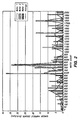
- FIG. 2 shows a comparison of wafer particle counts on wafers processed in a processing chamber having a hot-pressed silicon nitride gas distribution plate during an oxide etching process carried out for 20 seconds at a chamber pressure of 0.667 Pa (5 mTorr), TCP TM power (RF power supplied by antenna 18) at 1215 W, bottom electrode power (RF bias supplied by substrate holder 12) at 950 W with 30 sccm C 2 HF 5 and 20 sccmC 2 F 6 as the process gas.
- TCP TM power RF power supplied by antenna 18
- bottom electrode power RF bias supplied by substrate holder 12
- the silicon nitride gas distribution plate comprises a silicon nitride based material which can include an effective amount of a sintering aid such as a metal oxide sintering aid, e.g., MgO, Al 2 0 3 or SiO2.
- a sintering aid such as a metal oxide sintering aid, e.g., MgO, Al 2 0 3 or SiO2.
- Such sintering aids are preferably provided in an amount of no greater than 3 wt % of the material used to produce the gas distribution plate, thus greatly reducing the aluminum contamination on the wafers compared to the case in which an alumina gas distribution plate is used.
- FIG. 3 shows particle counts for the same process in the case where the gas distribution plate is made of alumina.
- the average particle contamination can be maintained below about 10 particles/wafer during a marathon run of 2000 wafers using the silicon nitride gas distribution plate whereas the average particle contamination was around 150 particles/wafer during a similar run using an alumina gas distribution plate.
- oxide etching polymer continuously builds-up on the alumina gas distribution plate and the built-up polymer flakes off and contaminates the wafers being processed.
- a highly intact and uniform passivating layer forms on the silicon nitride gas distribution plate.
- This passivating layer on the silicon nitride is very uniform in thickness (e.g., less than 10 ⁇ m) and grows very slowly compared to the rate of growth of the polymer build-up on alumina. Thus, the passivating layer on the silicon nitride does not lead to the flaking problem seen with alumina components.
- the gas distribution plate can have various designs such as those shown in FIGS. 4-7 .
- the gas distribution plate 40 shown in FIG. 4 includes eighty-nine holes 41 and four embossments 42 near the center thereof for providing a passage for supply gas between the gas distribution plate and the dielectric window.
- the gas distribution plate 50 shown in FIGS. 5-7 includes thirty-one holes 51, channels 52 for supplying process gas to the holes 51 and the plate is thicker at an outer periphery 54 thereof for purposes of mating with a mounting arrangement of the chamber.
- the gas distribution plate, liner and/or focus ring can be mounted in chambers of the types disclosed in commonly owned U.S. Patent Application Serial Nos. 08/658,261 and 08/658,262 .
- Substrates which are etched in an oxide etching process generally include an underlayer, an oxide layer which is to be etched, and a photoresist layer formed on top of the oxide layer.
- the oxide layer may be one of SiO 2 , BPSG,PSG, or other oxide material.
- the underlayer may be Si, TiN, silicide, or other underlying layer or substrate material.
- the etch selectivity, which is the etch rate of the layer to be etched compared to the photoresist etch rate is preferably around 4:1 or higher.
- the etch selectivity of the oxide layer compared to the underlayer is preferably greater than the oxide:photoresist etch selectively, e.g., 40:1.
- the silicon nitride liner, focus ring and/or gas distribution plate reduces particle contamination of substrates during processing such as etching of dielectric materials such as silicon dioxide (e.g., doped or undoped TEOS, BPSG,USG (undoped spin-on-glass), thermal oxide, plasma oxide, etc.) typically overlying a conductive layer such as silicon, polysilicon, silicide, titanium nitride, aluminum or a nonconductive material such as silicon nitride.
- dielectric materials such as silicon dioxide (e.g., doped or undoped TEOS, BPSG,USG (undoped spin-on-glass), thermal oxide, plasma oxide, etc.) typically overlying a conductive layer such as silicon, polysilicon, silicide, titanium nitride, aluminum or a nonconductive material such as silicon nitride.
- features such as contact holes, vias, trenches, etc.
- substrates such as semiconductor wafers (e.g., 25 or more consecutive wafers) while maintaining particle contamination of the wafers below acceptable levels.
- the chamber pressure is typically below 40 Pa (300 mTorr), preferably 0.13-5.33 Pa (1-40 mTorr)
- the antenna is powered at 200-5000 watts, preferably 300-2500 watts
- the RF bias is ⁇ 6000 watts, preferably 1000-2500 watts
- the He backpressure is 667-5,333 Pa (5-40 Torr), preferably 933-2,666 Pa (7-20 Torr).
- the process gas can include 10-200 sccmCHF 3 , 10-100 sccm C 2 HF 5 and/or 10-100 sccm C 2 F 6 .
- Temperature control of the gas distribution plate 22 can be provided by using channel 24 for circulating a fluid through the antenna 18 from a closed circuit temperature controller 28.
- the temperature controller preferably monitors the window temperature such as by one or more temperature sensors 27 and controls coolant temperature and/or flow rate of coolant through the antenna 18 to maintain the window below a threshold temperature.
- the antenna 18 is preferably in good thermal contact with the window 20 to provide adequate heat transfer between the window and the antenna 18.
- the window is preferably made of a high thermal conductivity dielectric material such as aluminum nitride which maximizes heat transfer from the antenna 18 through the window to the gas distribution plate 22.
- Aluminum nitride Properties of aluminum nitride include thermal conductivity of 100 w/m-k, density of 3.27 g/cm3, heat capacity of 0.2 cal/gm-k, and emissivity of 0.75.
- the heat which is received by the gas distribution plate 22 due to ion bombardment from the plasma is passed through the window 20 and can be removed by passing cooling fluid within the antenna 18, increasing gas pressure between the window and gas distribution plate 22, blowing cooling gas over the antenna and/or adding a light gas such as He to the process gas distributed by the gas distribution plate.
- the antenna 18 can have various shapes and profiles such as a substantially planar profile and/or a spiral shape having one or more (e.g., 3 to 7) turns in the spiral.
- the channel 24 preferably extends through all portions of the antenna 18 from a cooling fluid inlet to a cooling fluid outlet.
- the cooling fluid may flow from the exterior of the spiral antenna 18 toward the center, or from the center to the exterior thereof.
- the antenna may be bonded to the window by any suitable technique such as brazing, adhesive (e.g., RTV), etc., which provides good heat transfer characteristics between the antenna and the window.
- the cooling fluid which is passed through the antenna is preferably a non-conducting liquid such as deionized water, ethylene glycol, a conventional heat exchanger oil, or Fluoroinert (a dielectric fluid made by DuPont).
- the antenna can include a cooling tube which is bonded to a surface, such as a top surface, of the antenna. The cooling fluid is passed through the cooling tube in the same manner as the channel 24.
- the gas distribution plate 22 is preferably formed as a separate piece attachable to the reaction chamber.
- the window 20 and the gas distribution plate 22 may be formed as a single piece.
- higher thermal conductivity of the window/gas distribution plate 22 arrangement can be provided and/or the heat transfer across the window and the gas distribution plate 22 can be made more uniform.
- suitable gas passages and outlet holes can be provided in a green ceramic dielectric material which is later sintered to form a unitary plate.
- the dimensions of the passages and holes are preferably small enough to avoid conditions under which plasma would form during flow of process gas and powering of the antenna.
- the liner, focus ring and/or gas distribution plate can be made of various blends of silicon nitride based powder material having a predominant amount of silicon nitride.
- the total amount of silicon nitride can be at least 90 wt %, preferably ⁇ 95 wt %, and more preferably ⁇ 97 wt %.
- suitable compositions include (1) 97.37% Si 3 N 4 + 1.66 wt % MgO + 0.97% SiO 2 ; (2) 98.366% Si 3 N 4 + 0.908% MgO + 0.726% Al 2 O 3 ; (3) 97.496% Si 3 N 4 + 1.12% MgO + 0.487% SiO 2 + 0.897% Al 2 O 3 ; and (4) 96.639% Si 3 N 4 + 1.331% MgO + 0.966% SiO 2 + 1.064% Al 2 O 3 .
- the silicon and nitrogen are preferably present in amounts to sufficient achieve a nominal Si 3 N 4 stoichiometry.
- Such mixtures can be formed into a desired shape, sintered and machined to desired tolerances and/or surface finishes on surfaces such as vacuum sealing surfaces.
- the gas distribution plate can include any desired hole pattern.
- An example of a suitable pattern is shown in FIG. 4 wherein 89 holes having diameters of 0.051 cm (0.020 inch) are provided.
- the hole pattern includes a center hole, 4 holes on a 5.08 cm (2 inch) diameter, 6 holes on a 7.62 cm (3 inch) diameter, 6 holes on a 10.16 cm (4 inch) diameter, 8 holes on a 12.70 cm (5 inch) diameter, 8 holes on a 15.24 cm (6 inch) diameter, 12 holes on a 17.78 cm (7 inch) diameter, 12 holes on a 20.32 cm (8 inch) diameter, 16 holes on a 22.86 cm (9 inch) diameter, and 16 holes on a 25.4 cm (10 inch) diameter.
- the plate also includes 4 embossments 0.051 cm (0.020 inch) thick near the center of the plate for purposes of separating the plate from the overlying window.
- FIG. 5 shows a gas distribution plate according to the invention having 31 holes with 0.063 cm (0.025 inch) diameters.
- the hole pattern includes a center hole, 4 holes on a 5.08 cm (2 inch) diameter, 6 holes on a 10.16 cm (4 inch) diameter, 8 holes on a 15.24 cm (6 inch) diameter and 12 holes on a 20.32 cm (8 inch) diameter.
- the plate also includes a thicker outer edge thereof as shown in FIG. 6 .
- the surface of the plate facing the overlying window includes a pattern of rectangular grooves therein which distribute process gas to the gas outlets shown in FIG. 5 . As shown in FIG. 7, 6 radially extending grooves are provided which are each 0.038 cm (0.015 inch) deep and 0.889 cm (0.35 inch) wide.
- the antenna is preferably located such that portions thereof do not overlie any outlet holes in the gas distribution plate.
- the antenna comprises a multi-turn coil and the gas distribution plate includes a center hole and various holes located on one more circles at fixed radii from the center hole, the antenna is preferably located such that any turn passing through the circles is located between a pair of adjacent holes located on the circles. Such positioning of the antenna would minimize the possibility of striking a plasma in the holes located closest to the antenna.
- the silicon nitride gas distribution plate according to the invention provides dramatic reduction in particle count on wafers processed during oxide etching and oxygen cleaning steps. For instance, the silicon nitride gas distribution plate also reduces particle contamination during an ashing process wherein 750 sccm oxygen gas can be run for 10 seconds with the TCP TM power at 650 W, the bottom electrode at 750 W and the pressure at 10 mTorr.
- the silicon nitride gas distribution plate Compared to an alumina gas distribution plate which is attacked during the etching and oxygen cleaning steps and causes alumina particles to fall on wafers, the silicon nitride gas distribution plate provides better contamination performance since the bi-products produced when the silicon nitride material is attacked during the etching and oxygen cleaning steps are volatile and thus do not contribute to adding particles on the wafers.
- the silicon nitride gas distribution plate can be made in various ways.
- the silicon nitride can be hot pressed at temperatures above 1500°C using a powder that contains a high percentage of alpha silicon nitride.
- the alpha phase transforms to the beta-modification and transformation and densification is dependent on the pressure, temperature and alpha/beta phase ratio of the starting powders.
- Typical additives for silicon nitride include MgO, Y 2 O 3 , CeO 2 , ZrO 2 and Al 2 O 3 and possibly other rare-earth oxides.
- the hot pressing can be carried by processes such as hot isostatic pressing or gas pressure sintering.
- the gas pressure sintered material may exhibit a coarser structure with high aspect ratio grains whereas the pressed material may have a finer, more equiaxed structure.
- the gas pressure sintering may be conducted using nitrogen gas pressures up to 2 MPa wherein the nitrogen gas suppresses the thermal decomposition of silicon nitride and allows higher sintering temperatures to be used for densification.
- Hot pressed silicon nitride can be formed by the application of heat and uniaxial pressure in graphite dies heated by induction to temperatures in the range of 1650 to 1850°C for 1 to 4 hours under an applied stress of 15 to 30 MPa.
- Another technique involves firing a shaped component of silicon nitride at 1700 to 1800°C under a nitrogen atmosphere at 0.1 MPa.
- Another technique involves adding additives such as MgO or Y 2 O 3 with silicon prior to shaping and then nitration is carried out followed by firing in the range of 1800 to 2000°C under a nitrogen atmosphere.
- additives such as MgO or Y 2 O 3 with silicon prior to shaping and then nitration is carried out followed by firing in the range of 1800 to 2000°C under a nitrogen atmosphere.
- Other techniques for preparing the silicon nitride gas distribution plate according to the invention will be apparent to the skilled artisan.
Landscapes
- Physics & Mathematics (AREA)
- Engineering & Computer Science (AREA)
- Plasma & Fusion (AREA)
- Chemical & Material Sciences (AREA)
- Analytical Chemistry (AREA)
- Drying Of Semiconductors (AREA)
- Plasma Technology (AREA)
- Chemical Vapour Deposition (AREA)
- Physical Or Chemical Processes And Apparatus (AREA)
Applications Claiming Priority (3)
| Application Number | Priority Date | Filing Date | Title |
|---|---|---|---|
| US08/722,371 US5993594A (en) | 1996-09-30 | 1996-09-30 | Particle controlling method and apparatus for a plasma processing chamber |
| US722371 | 1996-09-30 | ||
| PCT/US1997/016133 WO1998014980A1 (en) | 1996-09-30 | 1997-09-17 | Particle controlling method and plasma processing chamber |
Related Child Applications (1)
| Application Number | Title | Priority Date | Filing Date |
|---|---|---|---|
| EP07023367 Division | 2007-12-03 |
Publications (2)
| Publication Number | Publication Date |
|---|---|
| EP0938740A1 EP0938740A1 (en) | 1999-09-01 |
| EP0938740B1 true EP0938740B1 (en) | 2008-12-03 |
Family
ID=24901571
Family Applications (1)
| Application Number | Title | Priority Date | Filing Date |
|---|---|---|---|
| EP97941540A Expired - Lifetime EP0938740B1 (en) | 1996-09-30 | 1997-09-17 | Particle controlling method and plasma processing chamber |
Country Status (7)
| Country | Link |
|---|---|
| US (2) | US5993594A (https=) |
| EP (1) | EP0938740B1 (https=) |
| JP (2) | JP4263245B2 (https=) |
| KR (2) | KR100615067B1 (https=) |
| AT (1) | ATE416474T1 (https=) |
| DE (1) | DE69739145D1 (https=) |
| WO (1) | WO1998014980A1 (https=) |
Families Citing this family (76)
| Publication number | Priority date | Publication date | Assignee | Title |
|---|---|---|---|---|
| US20010049196A1 (en) * | 1997-09-09 | 2001-12-06 | Roger Patrick | Apparatus for improving etch uniformity and methods therefor |
| US6120660A (en) * | 1998-02-11 | 2000-09-19 | Silicon Genesis Corporation | Removable liner design for plasma immersion ion implantation |
| US6129808A (en) * | 1998-03-31 | 2000-10-10 | Lam Research Corporation | Low contamination high density plasma etch chambers and methods for making the same |
| US6123791A (en) * | 1998-07-29 | 2000-09-26 | Applied Materials, Inc. | Ceramic composition for an apparatus and method for processing a substrate |
| US6074953A (en) * | 1998-08-28 | 2000-06-13 | Micron Technology, Inc. | Dual-source plasma etchers, dual-source plasma etching methods, and methods of forming planar coil dual-source plasma etchers |
| US6491042B1 (en) * | 1998-12-07 | 2002-12-10 | Taiwan Semiconductor Manufacturing Company | Post etching treatment process for high density oxide etcher |
| JP3542514B2 (ja) * | 1999-01-19 | 2004-07-14 | 株式会社日立製作所 | ドライエッチング装置 |
| US6408786B1 (en) * | 1999-09-23 | 2002-06-25 | Lam Research Corporation | Semiconductor processing equipment having tiled ceramic liner |
| JP2003533010A (ja) * | 1999-09-30 | 2003-11-05 | ラム リサーチ コーポレーション | 前処理を行なったガス整流板 |
| US6673198B1 (en) * | 1999-12-22 | 2004-01-06 | Lam Research Corporation | Semiconductor processing equipment having improved process drift control |
| US6391146B1 (en) | 2000-04-11 | 2002-05-21 | Applied Materials, Inc. | Erosion resistant gas energizer |
| US6440219B1 (en) * | 2000-06-07 | 2002-08-27 | Simplus Systems Corporation | Replaceable shielding apparatus |
| DE10134806A1 (de) * | 2000-08-10 | 2002-06-13 | Stratos Lightwave Inc N D Ges | Dampfphasenreaktionsvorrichtung mit Diaphragma für variable Stromverteilung |
| US7128804B2 (en) * | 2000-12-29 | 2006-10-31 | Lam Research Corporation | Corrosion resistant component of semiconductor processing equipment and method of manufacture thereof |
| US6805952B2 (en) * | 2000-12-29 | 2004-10-19 | Lam Research Corporation | Low contamination plasma chamber components and methods for making the same |
| JP5079949B2 (ja) * | 2001-04-06 | 2012-11-21 | 東京エレクトロン株式会社 | 処理装置および処理方法 |
| US6720259B2 (en) * | 2001-10-02 | 2004-04-13 | Genus, Inc. | Passivation method for improved uniformity and repeatability for atomic layer deposition and chemical vapor deposition |
| US6942929B2 (en) | 2002-01-08 | 2005-09-13 | Nianci Han | Process chamber having component with yttrium-aluminum coating |
| US7371467B2 (en) | 2002-01-08 | 2008-05-13 | Applied Materials, Inc. | Process chamber component having electroplated yttrium containing coating |
| US7479304B2 (en) * | 2002-02-14 | 2009-01-20 | Applied Materials, Inc. | Gas distribution plate fabricated from a solid yttrium oxide-comprising substrate |
| TWI225668B (en) * | 2002-05-13 | 2004-12-21 | Tokyo Electron Ltd | Substrate processing method |
| US7527706B2 (en) * | 2002-10-10 | 2009-05-05 | Tokyo Electron Limited | Plasma processing apparatus, process vessel for plasma processing apparatus and dielectric plate for plasma processing apparatus |
| US20060226003A1 (en) * | 2003-01-22 | 2006-10-12 | John Mize | Apparatus and methods for ionized deposition of a film or thin layer |
| US6749684B1 (en) | 2003-06-10 | 2004-06-15 | International Business Machines Corporation | Method for improving CVD film quality utilizing polysilicon getterer |
| US7713380B2 (en) * | 2004-01-27 | 2010-05-11 | Taiwan Semiconductor Manufacturing Co., Ltd. | Method and apparatus for backside polymer reduction in dry-etch process |
| US8540843B2 (en) * | 2004-06-30 | 2013-09-24 | Lam Research Corporation | Plasma chamber top piece assembly |
| US7578945B2 (en) * | 2004-09-27 | 2009-08-25 | Lam Research Corporation | Method and apparatus for tuning a set of plasma processing steps |
| US7138067B2 (en) * | 2004-09-27 | 2006-11-21 | Lam Research Corporation | Methods and apparatus for tuning a set of plasma processing steps |
| US20060151116A1 (en) * | 2005-01-12 | 2006-07-13 | Taiwan Semiconductor Manufacturing Co., Ltd. | Focus rings, apparatus in chamber, contact hole and method of forming contact hole |
| US9659758B2 (en) | 2005-03-22 | 2017-05-23 | Honeywell International Inc. | Coils utilized in vapor deposition applications and methods of production |
| US20060278520A1 (en) * | 2005-06-13 | 2006-12-14 | Lee Eal H | Use of DC magnetron sputtering systems |
| US20070079936A1 (en) * | 2005-09-29 | 2007-04-12 | Applied Materials, Inc. | Bonded multi-layer RF window |
| US20070235320A1 (en) * | 2006-04-06 | 2007-10-11 | Applied Materials, Inc. | Reactive sputtering chamber with gas distribution tubes |
| KR100798352B1 (ko) | 2006-05-24 | 2008-01-28 | 주식회사 뉴파워 프라즈마 | 다중 배열된 방전실을 갖는 플라즈마 반응기 및 이를이용한 플라즈마 처리 시스템 |
| US7674662B2 (en) * | 2006-07-19 | 2010-03-09 | Applied Materials, Inc. | Process for making thin film field effect transistors using zinc oxide |
| US7927713B2 (en) * | 2007-04-27 | 2011-04-19 | Applied Materials, Inc. | Thin film semiconductor material produced through reactive sputtering of zinc target using nitrogen gases |
| US10622194B2 (en) | 2007-04-27 | 2020-04-14 | Applied Materials, Inc. | Bulk sintered solid solution ceramic which exhibits fracture toughness and halogen plasma resistance |
| US10242888B2 (en) | 2007-04-27 | 2019-03-26 | Applied Materials, Inc. | Semiconductor processing apparatus with a ceramic-comprising surface which exhibits fracture toughness and halogen plasma resistance |
| US7972471B2 (en) * | 2007-06-29 | 2011-07-05 | Lam Research Corporation | Inductively coupled dual zone processing chamber with single planar antenna |
| WO2009018509A1 (en) * | 2007-08-02 | 2009-02-05 | Applied Materials, Inc. | Thin film transistors using thin film semiconductor materials |
| US8202393B2 (en) * | 2007-08-29 | 2012-06-19 | Lam Research Corporation | Alternate gas delivery and evacuation system for plasma processing apparatuses |
| KR101645043B1 (ko) * | 2007-10-31 | 2016-08-02 | 램 리써치 코포레이션 | 플라즈마 프로세싱 챔버, 플라즈마 프로세싱 콤포넌트 및 플라즈마 식각 챔버 프로세싱 콤포넌트 제조 방법 |
| US8980066B2 (en) * | 2008-03-14 | 2015-03-17 | Applied Materials, Inc. | Thin film metal oxynitride semiconductors |
| WO2009117438A2 (en) | 2008-03-20 | 2009-09-24 | Applied Materials, Inc. | Process to make metal oxide thin film transistor array with etch stopping layer |
| US7879698B2 (en) * | 2008-03-24 | 2011-02-01 | Applied Materials, Inc. | Integrated process system and process sequence for production of thin film transistor arrays using doped or compounded metal oxide semiconductor |
| US8258511B2 (en) | 2008-07-02 | 2012-09-04 | Applied Materials, Inc. | Thin film transistors using multiple active channel layers |
| KR101013511B1 (ko) | 2008-08-12 | 2011-02-10 | 주식회사 맥시스 | 라이너 어셈블리 및 이를 구비하는 플라즈마 처리 장치 |
| US8313612B2 (en) * | 2009-03-24 | 2012-11-20 | Lam Research Corporation | Method and apparatus for reduction of voltage potential spike during dechucking |
| KR101733718B1 (ko) | 2009-09-24 | 2017-05-10 | 어플라이드 머티어리얼스, 인코포레이티드 | 소스 및 드레인 금속 식각을 위해 습식 프로세스를 이용하여 금속 산화물 또는 금속 산질화물 tft들을 제조하는 방법들 |
| US8840763B2 (en) | 2009-09-28 | 2014-09-23 | Applied Materials, Inc. | Methods for stable process in a reactive sputtering process using zinc or doped zinc target |
| JP5592098B2 (ja) | 2009-10-27 | 2014-09-17 | 東京エレクトロン株式会社 | プラズマ処理装置及びプラズマ処理方法 |
| JP5851681B2 (ja) * | 2009-10-27 | 2016-02-03 | 東京エレクトロン株式会社 | プラズマ処理装置 |
| KR101757922B1 (ko) * | 2009-10-27 | 2017-07-14 | 도쿄엘렉트론가부시키가이샤 | 플라즈마 처리 장치 |
| US9313872B2 (en) | 2009-10-27 | 2016-04-12 | Tokyo Electron Limited | Plasma processing apparatus and plasma processing method |
| US9120985B2 (en) | 2010-05-26 | 2015-09-01 | Exxonmobil Research And Engineering Company | Corrosion resistant gasifier components |
| US8562785B2 (en) * | 2011-05-31 | 2013-10-22 | Lam Research Corporation | Gas distribution showerhead for inductively coupled plasma etch reactor |
| JP5617817B2 (ja) * | 2011-10-27 | 2014-11-05 | パナソニック株式会社 | 誘導結合型プラズマ処理装置及び誘導結合型プラズマ処理方法 |
| SG11201402058TA (en) * | 2011-11-24 | 2014-09-26 | Lam Res Corp | Symmetric rf return path liner |
| US10115565B2 (en) | 2012-03-02 | 2018-10-30 | Panasonic Intellectual Property Management Co., Ltd. | Plasma processing apparatus and plasma processing method |
| US20140097752A1 (en) * | 2012-10-09 | 2014-04-10 | Varian Semiconductor Equipment Associates, Inc. | Inductively Coupled Plasma ION Source Chamber with Dopant Material Shield |
| US9314854B2 (en) | 2013-01-30 | 2016-04-19 | Lam Research Corporation | Ductile mode drilling methods for brittle components of plasma processing apparatuses |
| JP2014149983A (ja) * | 2013-02-01 | 2014-08-21 | Toshiba Corp | プラズマ処理装置用電極とその製造方法、及びプラズマ処理装置 |
| US8893702B2 (en) | 2013-02-20 | 2014-11-25 | Lam Research Corporation | Ductile mode machining methods for hard and brittle components of plasma processing apparatuses |
| US20140356985A1 (en) | 2013-06-03 | 2014-12-04 | Lam Research Corporation | Temperature controlled substrate support assembly |
| US10249511B2 (en) * | 2014-06-27 | 2019-04-02 | Lam Research Corporation | Ceramic showerhead including central gas injector for tunable convective-diffusive gas flow in semiconductor substrate processing apparatus |
| US10504700B2 (en) * | 2015-08-27 | 2019-12-10 | Applied Materials, Inc. | Plasma etching systems and methods with secondary plasma injection |
| WO2017127163A1 (en) * | 2016-01-22 | 2017-07-27 | Applied Materials, Inc. | Ceramic showerhead with embedded conductive layers |
| WO2017218044A1 (en) * | 2016-06-15 | 2017-12-21 | Applied Materials, Inc. | Gas distribution plate assembly for high power plasma etch processes |
| US10504720B2 (en) * | 2016-11-29 | 2019-12-10 | Taiwan Semiconductor Manufacturing Company, Ltd. | Etching using chamber with top plate formed of non-oxygen containing material |
| US11183373B2 (en) | 2017-10-11 | 2021-11-23 | Honeywell International Inc. | Multi-patterned sputter traps and methods of making |
| CN107600735A (zh) * | 2017-10-22 | 2018-01-19 | 惠州市通用纸业有限公司 | 一种便于取拿纸巾的环保型双用纸巾包装袋 |
| US11222794B2 (en) * | 2018-03-30 | 2022-01-11 | Taiwan Semiconductor Manufacturing Co., Ltd | Semiconductor fabrication system embedded with effective baking module |
| CN112071733B (zh) * | 2019-06-10 | 2024-03-12 | 中微半导体设备(上海)股份有限公司 | 用于真空处理设备的内衬装置和真空处理设备 |
| JP7426709B2 (ja) * | 2019-10-23 | 2024-02-02 | 株式会社イー・エム・ディー | プラズマ源 |
| US12562355B2 (en) | 2021-04-13 | 2026-02-24 | Applied Materials, Inc. | Isolator for processing chambers |
| KR102646591B1 (ko) * | 2022-05-13 | 2024-03-12 | 세메스 주식회사 | 기판 처리 장치 |
Family Cites Families (30)
| Publication number | Priority date | Publication date | Assignee | Title |
|---|---|---|---|---|
| US5445776A (en) * | 1980-10-20 | 1995-08-29 | Kabushiki Kaisha Kobe Seiko Sho | Method for producing high density sintered silicon nitride (Si3 N.sub.4 |
| US4340462A (en) * | 1981-02-13 | 1982-07-20 | Lam Research Corporation | Adjustable electrode plasma processing chamber |
| US4579618A (en) * | 1984-01-06 | 1986-04-01 | Tegal Corporation | Plasma reactor apparatus |
| DE3662872D1 (en) * | 1986-11-25 | 1989-05-24 | Battelle Memorial Institute | Pulverulent silicon nitride composition reinforced with silicon carbide whiskers and its use for the manufacturing of sintered parts |
| US5262029A (en) * | 1988-05-23 | 1993-11-16 | Lam Research | Method and system for clamping semiconductor wafers |
| JPH02229431A (ja) * | 1989-03-02 | 1990-09-12 | Fujitsu Ltd | 半導体装置の製造方法 |
| GB8905073D0 (en) * | 1989-03-06 | 1989-04-19 | Nordiko Ltd | Ion gun |
| JPH02298024A (ja) * | 1989-05-12 | 1990-12-10 | Tadahiro Omi | リアクティブイオンエッチング装置 |
| US4948458A (en) * | 1989-08-14 | 1990-08-14 | Lam Research Corporation | Method and apparatus for producing magnetically-coupled planar plasma |
| US5304279A (en) * | 1990-08-10 | 1994-04-19 | International Business Machines Corporation | Radio frequency induction/multipole plasma processing tool |
| US5304248A (en) * | 1990-12-05 | 1994-04-19 | Applied Materials, Inc. | Passive shield for CVD wafer processing which provides frontside edge exclusion and prevents backside depositions |
| US5200232A (en) * | 1990-12-11 | 1993-04-06 | Lam Research Corporation | Reaction chamber design and method to minimize particle generation in chemical vapor deposition reactors |
| JPH05198534A (ja) * | 1992-01-20 | 1993-08-06 | Sony Corp | ドライエッチング方法 |
| US5241245A (en) * | 1992-05-06 | 1993-08-31 | International Business Machines Corporation | Optimized helical resonator for plasma processing |
| US5226967A (en) * | 1992-05-14 | 1993-07-13 | Lam Research Corporation | Plasma apparatus including dielectric window for inducing a uniform electric field in a plasma chamber |
| US5460684A (en) * | 1992-12-04 | 1995-10-24 | Tokyo Electron Limited | Stage having electrostatic chuck and plasma processing apparatus using same |
| US5401350A (en) * | 1993-03-08 | 1995-03-28 | Lsi Logic Corporation | Coil configurations for improved uniformity in inductively coupled plasma systems |
| JPH06310065A (ja) * | 1993-04-26 | 1994-11-04 | Nissin Electric Co Ltd | イオン源装置 |
| US5531834A (en) * | 1993-07-13 | 1996-07-02 | Tokyo Electron Kabushiki Kaisha | Plasma film forming method and apparatus and plasma processing apparatus |
| JP3276023B2 (ja) * | 1993-10-20 | 2002-04-22 | 東京エレクトロン株式会社 | プラズマ処理装置の制御方法 |
| US5529657A (en) * | 1993-10-04 | 1996-06-25 | Tokyo Electron Limited | Plasma processing apparatus |
| GB9321489D0 (en) * | 1993-10-19 | 1993-12-08 | Central Research Lab Ltd | Plasma processing |
| TW293983B (https=) * | 1993-12-17 | 1996-12-21 | Tokyo Electron Co Ltd | |
| JP3308091B2 (ja) * | 1994-02-03 | 2002-07-29 | 東京エレクトロン株式会社 | 表面処理方法およびプラズマ処理装置 |
| US5580385A (en) * | 1994-06-30 | 1996-12-03 | Texas Instruments, Incorporated | Structure and method for incorporating an inductively coupled plasma source in a plasma processing chamber |
| US5746875A (en) * | 1994-09-16 | 1998-05-05 | Applied Materials, Inc. | Gas injection slit nozzle for a plasma process reactor |
| US5762714A (en) * | 1994-10-18 | 1998-06-09 | Applied Materials, Inc. | Plasma guard for chamber equipped with electrostatic chuck |
| US5671116A (en) | 1995-03-10 | 1997-09-23 | Lam Research Corporation | Multilayered electrostatic chuck and method of manufacture thereof |
| US5824605A (en) | 1995-07-31 | 1998-10-20 | Lam Research Corporation | Gas dispersion window for plasma apparatus and method of use thereof |
| US5863376A (en) | 1996-06-05 | 1999-01-26 | Lam Research Corporation | Temperature controlling method and apparatus for a plasma processing chamber |
-
1996
- 1996-09-30 US US08/722,371 patent/US5993594A/en not_active Expired - Lifetime
-
1997
- 1997-09-17 KR KR1019997002516A patent/KR100615067B1/ko not_active Expired - Fee Related
- 1997-09-17 JP JP51655898A patent/JP4263245B2/ja not_active Expired - Fee Related
- 1997-09-17 AT AT97941540T patent/ATE416474T1/de not_active IP Right Cessation
- 1997-09-17 EP EP97941540A patent/EP0938740B1/en not_active Expired - Lifetime
- 1997-09-17 DE DE69739145T patent/DE69739145D1/de not_active Expired - Lifetime
- 1997-09-17 KR KR1020057006799A patent/KR100665649B1/ko not_active Expired - Fee Related
- 1997-09-17 WO PCT/US1997/016133 patent/WO1998014980A1/en not_active Ceased
-
1999
- 1999-06-09 US US09/328,793 patent/US6251793B1/en not_active Expired - Lifetime
-
2008
- 2008-04-22 JP JP2008111896A patent/JP4891287B2/ja not_active Expired - Fee Related
Also Published As
| Publication number | Publication date |
|---|---|
| KR100665649B1 (ko) | 2007-01-09 |
| DE69739145D1 (de) | 2009-01-15 |
| WO1998014980A1 (en) | 1998-04-09 |
| JP4891287B2 (ja) | 2012-03-07 |
| KR20060029592A (ko) | 2006-04-06 |
| JP2008235924A (ja) | 2008-10-02 |
| EP0938740A1 (en) | 1999-09-01 |
| US5993594A (en) | 1999-11-30 |
| KR100615067B1 (ko) | 2006-08-22 |
| ATE416474T1 (de) | 2008-12-15 |
| US6251793B1 (en) | 2001-06-26 |
| KR20000048585A (ko) | 2000-07-25 |
| JP4263245B2 (ja) | 2009-05-13 |
| JP2001501379A (ja) | 2001-01-30 |
Similar Documents
| Publication | Publication Date | Title |
|---|---|---|
| EP0938740B1 (en) | Particle controlling method and plasma processing chamber | |
| EP1068632B1 (en) | Contamination controlling method and plasma processing chamber | |
| US6464843B1 (en) | Contamination controlling method and apparatus for a plasma processing chamber | |
| US6033585A (en) | Method and apparatus for preventing lightup of gas distribution holes | |
| EP1145273B1 (en) | Low contamination high density plasma etch chambers and methods for making the same | |
| US6451157B1 (en) | Gas distribution apparatus for semiconductor processing | |
| CN101889329B (zh) | 长寿命可消耗氮化硅-二氧化硅等离子处理部件 | |
| US6048798A (en) | Apparatus for reducing process drift in inductive coupled plasma etching such as oxide layer | |
| TWI417957B (zh) | 具有介電間隔環之邊緣環總成 | |
| US8118936B2 (en) | Method and apparatus for an improved baffle plate in a plasma processing system | |
| US7566368B2 (en) | Method and apparatus for an improved upper electrode plate in a plasma processing system | |
| KR20040038875A (ko) | 유전체 식각 방법 | |
| US20250191893A1 (en) | Spark plasma sintered component for cryo-plasma processing |
Legal Events
| Date | Code | Title | Description |
|---|---|---|---|
| PUAI | Public reference made under article 153(3) epc to a published international application that has entered the european phase |
Free format text: ORIGINAL CODE: 0009012 |
|
| 17P | Request for examination filed |
Effective date: 19990427 |
|
| AK | Designated contracting states |
Kind code of ref document: A1 Designated state(s): AT DE FR GB IE IT |
|
| 17Q | First examination report despatched |
Effective date: 20050118 |
|
| GRAP | Despatch of communication of intention to grant a patent |
Free format text: ORIGINAL CODE: EPIDOSNIGR1 |
|
| GRAS | Grant fee paid |
Free format text: ORIGINAL CODE: EPIDOSNIGR3 |
|
| GRAS | Grant fee paid |
Free format text: ORIGINAL CODE: EPIDOSNIGR3 |
|
| GRAA | (expected) grant |
Free format text: ORIGINAL CODE: 0009210 |
|
| AK | Designated contracting states |
Kind code of ref document: B1 Designated state(s): AT DE FR GB IE IT |
|
| REG | Reference to a national code |
Ref country code: GB Ref legal event code: FG4D |
|
| REG | Reference to a national code |
Ref country code: IE Ref legal event code: FG4D |
|
| REF | Corresponds to: |
Ref document number: 69739145 Country of ref document: DE Date of ref document: 20090115 Kind code of ref document: P |
|
| PG25 | Lapsed in a contracting state [announced via postgrant information from national office to epo] |
Ref country code: AT Free format text: LAPSE BECAUSE OF FAILURE TO SUBMIT A TRANSLATION OF THE DESCRIPTION OR TO PAY THE FEE WITHIN THE PRESCRIBED TIME-LIMIT Effective date: 20081203 |
|
| PLBE | No opposition filed within time limit |
Free format text: ORIGINAL CODE: 0009261 |
|
| STAA | Information on the status of an ep patent application or granted ep patent |
Free format text: STATUS: NO OPPOSITION FILED WITHIN TIME LIMIT |
|
| 26N | No opposition filed |
Effective date: 20090904 |
|
| GBPC | Gb: european patent ceased through non-payment of renewal fee |
Effective date: 20090917 |
|
| PG25 | Lapsed in a contracting state [announced via postgrant information from national office to epo] |
Ref country code: IE Free format text: LAPSE BECAUSE OF NON-PAYMENT OF DUE FEES Effective date: 20090917 |
|
| PG25 | Lapsed in a contracting state [announced via postgrant information from national office to epo] |
Ref country code: GB Free format text: LAPSE BECAUSE OF NON-PAYMENT OF DUE FEES Effective date: 20090917 |
|
| PG25 | Lapsed in a contracting state [announced via postgrant information from national office to epo] |
Ref country code: IT Free format text: LAPSE BECAUSE OF FAILURE TO SUBMIT A TRANSLATION OF THE DESCRIPTION OR TO PAY THE FEE WITHIN THE PRESCRIBED TIME-LIMIT Effective date: 20081203 |
|
| PGFP | Annual fee paid to national office [announced via postgrant information from national office to epo] |
Ref country code: DE Payment date: 20130927 Year of fee payment: 17 |
|
| PGFP | Annual fee paid to national office [announced via postgrant information from national office to epo] |
Ref country code: FR Payment date: 20130919 Year of fee payment: 17 |
|
| REG | Reference to a national code |
Ref country code: DE Ref legal event code: R119 Ref document number: 69739145 Country of ref document: DE |
|
| REG | Reference to a national code |
Ref country code: FR Ref legal event code: ST Effective date: 20150529 |
|
| PG25 | Lapsed in a contracting state [announced via postgrant information from national office to epo] |
Ref country code: DE Free format text: LAPSE BECAUSE OF NON-PAYMENT OF DUE FEES Effective date: 20150401 |
|
| PG25 | Lapsed in a contracting state [announced via postgrant information from national office to epo] |
Ref country code: FR Free format text: LAPSE BECAUSE OF NON-PAYMENT OF DUE FEES Effective date: 20140930 |