EP0924080B1 - Substrat für Tintenstrahlaufzeichnungskopf - Google Patents
Substrat für Tintenstrahlaufzeichnungskopf Download PDFInfo
- Publication number
- EP0924080B1 EP0924080B1 EP98124319A EP98124319A EP0924080B1 EP 0924080 B1 EP0924080 B1 EP 0924080B1 EP 98124319 A EP98124319 A EP 98124319A EP 98124319 A EP98124319 A EP 98124319A EP 0924080 B1 EP0924080 B1 EP 0924080B1
- Authority
- EP
- European Patent Office
- Prior art keywords
- ink jet
- jet recording
- ink
- recording head
- substrate
- Prior art date
- Legal status (The legal status is an assumption and is not a legal conclusion. Google has not performed a legal analysis and makes no representation as to the accuracy of the status listed.)
- Expired - Lifetime
Links
- 239000000758 substrate Substances 0.000 title claims description 60
- 239000005871 repellent Substances 0.000 claims description 35
- 238000000034 method Methods 0.000 claims description 33
- 230000008569 process Effects 0.000 claims description 16
- 229910052731 fluorine Inorganic materials 0.000 claims description 10
- 238000007599 discharging Methods 0.000 claims description 5
- 230000020169 heat generation Effects 0.000 claims description 3
- 229910052715 tantalum Inorganic materials 0.000 claims description 3
- PXGOKWXKJXAPGV-UHFFFAOYSA-N Fluorine Chemical compound FF PXGOKWXKJXAPGV-UHFFFAOYSA-N 0.000 claims description 2
- 239000011737 fluorine Substances 0.000 claims description 2
- GUVRBAGPIYLISA-UHFFFAOYSA-N tantalum atom Chemical compound [Ta] GUVRBAGPIYLISA-UHFFFAOYSA-N 0.000 claims description 2
- 239000010410 layer Substances 0.000 description 30
- 239000007788 liquid Substances 0.000 description 27
- 229910052581 Si3N4 Inorganic materials 0.000 description 10
- 230000015572 biosynthetic process Effects 0.000 description 10
- HQVNEWCFYHHQES-UHFFFAOYSA-N silicon nitride Chemical compound N12[Si]34N5[Si]62N3[Si]51N64 HQVNEWCFYHHQES-UHFFFAOYSA-N 0.000 description 10
- VYPSYNLAJGMNEJ-UHFFFAOYSA-N Silicium dioxide Chemical compound O=[Si]=O VYPSYNLAJGMNEJ-UHFFFAOYSA-N 0.000 description 9
- 229910052814 silicon oxide Inorganic materials 0.000 description 9
- 230000003213 activating effect Effects 0.000 description 8
- 125000001153 fluoro group Chemical group F* 0.000 description 8
- 239000000126 substance Substances 0.000 description 8
- 239000000463 material Substances 0.000 description 7
- XUIMIQQOPSSXEZ-UHFFFAOYSA-N Silicon Chemical compound [Si] XUIMIQQOPSSXEZ-UHFFFAOYSA-N 0.000 description 6
- 238000005229 chemical vapour deposition Methods 0.000 description 6
- 238000009413 insulation Methods 0.000 description 6
- 229910052710 silicon Inorganic materials 0.000 description 6
- 239000010703 silicon Substances 0.000 description 6
- 239000011229 interlayer Substances 0.000 description 5
- 150000002500 ions Chemical class 0.000 description 5
- 238000004140 cleaning Methods 0.000 description 4
- 239000003086 colorant Substances 0.000 description 4
- 238000005187 foaming Methods 0.000 description 4
- 238000004519 manufacturing process Methods 0.000 description 4
- KFZMGEQAYNKOFK-UHFFFAOYSA-N Isopropanol Chemical compound CC(C)O KFZMGEQAYNKOFK-UHFFFAOYSA-N 0.000 description 3
- 238000009825 accumulation Methods 0.000 description 3
- 125000004429 atom Chemical group 0.000 description 3
- 230000008859 change Effects 0.000 description 3
- 238000006243 chemical reaction Methods 0.000 description 3
- 150000001875 compounds Chemical class 0.000 description 3
- 230000007547 defect Effects 0.000 description 3
- 238000009792 diffusion process Methods 0.000 description 3
- 238000005516 engineering process Methods 0.000 description 3
- 239000012535 impurity Substances 0.000 description 3
- 239000005360 phosphosilicate glass Substances 0.000 description 3
- 239000000047 product Substances 0.000 description 3
- 238000011084 recovery Methods 0.000 description 3
- 239000004065 semiconductor Substances 0.000 description 3
- -1 TaN Chemical class 0.000 description 2
- 230000008901 benefit Effects 0.000 description 2
- 230000005540 biological transmission Effects 0.000 description 2
- 238000009835 boiling Methods 0.000 description 2
- 239000011248 coating agent Substances 0.000 description 2
- 238000000576 coating method Methods 0.000 description 2
- 230000007797 corrosion Effects 0.000 description 2
- 238000005260 corrosion Methods 0.000 description 2
- 230000002950 deficient Effects 0.000 description 2
- 238000010790 dilution Methods 0.000 description 2
- 239000012895 dilution Substances 0.000 description 2
- 239000011521 glass Substances 0.000 description 2
- 238000002347 injection Methods 0.000 description 2
- 239000007924 injection Substances 0.000 description 2
- 238000009434 installation Methods 0.000 description 2
- 239000007769 metal material Substances 0.000 description 2
- 230000003647 oxidation Effects 0.000 description 2
- 238000007254 oxidation reaction Methods 0.000 description 2
- 238000000059 patterning Methods 0.000 description 2
- 238000000206 photolithography Methods 0.000 description 2
- 238000005268 plasma chemical vapour deposition Methods 0.000 description 2
- 238000001454 recorded image Methods 0.000 description 2
- 239000011347 resin Substances 0.000 description 2
- 229920005989 resin Polymers 0.000 description 2
- 238000004544 sputter deposition Methods 0.000 description 2
- 229910000838 Al alloy Inorganic materials 0.000 description 1
- 229910018125 Al-Si Inorganic materials 0.000 description 1
- 229910018182 Al—Cu Inorganic materials 0.000 description 1
- 229910018520 Al—Si Inorganic materials 0.000 description 1
- 239000005977 Ethylene Substances 0.000 description 1
- GRYLNZFGIOXLOG-UHFFFAOYSA-N Nitric acid Chemical compound O[N+]([O-])=O GRYLNZFGIOXLOG-UHFFFAOYSA-N 0.000 description 1
- 239000004809 Teflon Substances 0.000 description 1
- 229920006362 Teflon® Polymers 0.000 description 1
- 230000009471 action Effects 0.000 description 1
- 239000012670 alkaline solution Substances 0.000 description 1
- 238000000137 annealing Methods 0.000 description 1
- 238000005345 coagulation Methods 0.000 description 1
- 230000015271 coagulation Effects 0.000 description 1
- 239000004020 conductor Substances 0.000 description 1
- 239000013078 crystal Substances 0.000 description 1
- 238000000354 decomposition reaction Methods 0.000 description 1
- 230000000694 effects Effects 0.000 description 1
- 125000000816 ethylene group Chemical group [H]C([H])([*:1])C([H])([H])[*:2] 0.000 description 1
- 238000001125 extrusion Methods 0.000 description 1
- 150000002222 fluorine compounds Chemical class 0.000 description 1
- 229920002313 fluoropolymer Polymers 0.000 description 1
- 239000004811 fluoropolymer Substances 0.000 description 1
- 238000009499 grossing Methods 0.000 description 1
- 238000010438 heat treatment Methods 0.000 description 1
- 230000006872 improvement Effects 0.000 description 1
- 229910010272 inorganic material Inorganic materials 0.000 description 1
- 239000011147 inorganic material Substances 0.000 description 1
- 239000012212 insulator Substances 0.000 description 1
- 238000005468 ion implantation Methods 0.000 description 1
- 238000011031 large-scale manufacturing process Methods 0.000 description 1
- 239000012528 membrane Substances 0.000 description 1
- 230000005499 meniscus Effects 0.000 description 1
- 229910044991 metal oxide Inorganic materials 0.000 description 1
- 150000004706 metal oxides Chemical class 0.000 description 1
- 125000000956 methoxy group Chemical group [H]C([H])([H])O* 0.000 description 1
- 229910017604 nitric acid Inorganic materials 0.000 description 1
- 150000004767 nitrides Chemical class 0.000 description 1
- 239000012466 permeate Substances 0.000 description 1
- 229920002492 poly(sulfone) Polymers 0.000 description 1
- 229910021420 polycrystalline silicon Inorganic materials 0.000 description 1
- 229920005591 polysilicon Polymers 0.000 description 1
- 230000009467 reduction Effects 0.000 description 1
- 230000000717 retained effect Effects 0.000 description 1
- 238000000926 separation method Methods 0.000 description 1
- 230000035939 shock Effects 0.000 description 1
- 229910000077 silane Inorganic materials 0.000 description 1
- 239000002210 silicon-based material Substances 0.000 description 1
- 239000002904 solvent Substances 0.000 description 1
- 238000004528 spin coating Methods 0.000 description 1
Images


Classifications
-
- B—PERFORMING OPERATIONS; TRANSPORTING
- B41—PRINTING; LINING MACHINES; TYPEWRITERS; STAMPS
- B41J—TYPEWRITERS; SELECTIVE PRINTING MECHANISMS, i.e. MECHANISMS PRINTING OTHERWISE THAN FROM A FORME; CORRECTION OF TYPOGRAPHICAL ERRORS
- B41J2/00—Typewriters or selective printing mechanisms characterised by the printing or marking process for which they are designed
- B41J2/005—Typewriters or selective printing mechanisms characterised by the printing or marking process for which they are designed characterised by bringing liquid or particles selectively into contact with a printing material
- B41J2/01—Ink jet
- B41J2/135—Nozzles
- B41J2/14—Structure thereof only for on-demand ink jet heads
- B41J2/14016—Structure of bubble jet print heads
- B41J2/14088—Structure of heating means
- B41J2/14112—Resistive element
- B41J2/14129—Layer structure
-
- B—PERFORMING OPERATIONS; TRANSPORTING
- B41—PRINTING; LINING MACHINES; TYPEWRITERS; STAMPS
- B41J—TYPEWRITERS; SELECTIVE PRINTING MECHANISMS, i.e. MECHANISMS PRINTING OTHERWISE THAN FROM A FORME; CORRECTION OF TYPOGRAPHICAL ERRORS
- B41J2/00—Typewriters or selective printing mechanisms characterised by the printing or marking process for which they are designed
- B41J2/005—Typewriters or selective printing mechanisms characterised by the printing or marking process for which they are designed characterised by bringing liquid or particles selectively into contact with a printing material
- B41J2/01—Ink jet
- B41J2/135—Nozzles
- B41J2/14—Structure thereof only for on-demand ink jet heads
- B41J2/14016—Structure of bubble jet print heads
- B41J2/14032—Structure of the pressure chamber
-
- B—PERFORMING OPERATIONS; TRANSPORTING
- B41—PRINTING; LINING MACHINES; TYPEWRITERS; STAMPS
- B41J—TYPEWRITERS; SELECTIVE PRINTING MECHANISMS, i.e. MECHANISMS PRINTING OTHERWISE THAN FROM A FORME; CORRECTION OF TYPOGRAPHICAL ERRORS
- B41J2/00—Typewriters or selective printing mechanisms characterised by the printing or marking process for which they are designed
- B41J2/005—Typewriters or selective printing mechanisms characterised by the printing or marking process for which they are designed characterised by bringing liquid or particles selectively into contact with a printing material
- B41J2/01—Ink jet
- B41J2/135—Nozzles
- B41J2/14—Structure thereof only for on-demand ink jet heads
- B41J2/14016—Structure of bubble jet print heads
- B41J2/14072—Electrical connections, e.g. details on electrodes, connecting the chip to the outside...
-
- B—PERFORMING OPERATIONS; TRANSPORTING
- B41—PRINTING; LINING MACHINES; TYPEWRITERS; STAMPS
- B41J—TYPEWRITERS; SELECTIVE PRINTING MECHANISMS, i.e. MECHANISMS PRINTING OTHERWISE THAN FROM A FORME; CORRECTION OF TYPOGRAPHICAL ERRORS
- B41J2/00—Typewriters or selective printing mechanisms characterised by the printing or marking process for which they are designed
- B41J2/005—Typewriters or selective printing mechanisms characterised by the printing or marking process for which they are designed characterised by bringing liquid or particles selectively into contact with a printing material
- B41J2/01—Ink jet
- B41J2/135—Nozzles
- B41J2/16—Production of nozzles
- B41J2/1601—Production of bubble jet print heads
- B41J2/1604—Production of bubble jet print heads of the edge shooter type
-
- B—PERFORMING OPERATIONS; TRANSPORTING
- B41—PRINTING; LINING MACHINES; TYPEWRITERS; STAMPS
- B41J—TYPEWRITERS; SELECTIVE PRINTING MECHANISMS, i.e. MECHANISMS PRINTING OTHERWISE THAN FROM A FORME; CORRECTION OF TYPOGRAPHICAL ERRORS
- B41J2/00—Typewriters or selective printing mechanisms characterised by the printing or marking process for which they are designed
- B41J2/005—Typewriters or selective printing mechanisms characterised by the printing or marking process for which they are designed characterised by bringing liquid or particles selectively into contact with a printing material
- B41J2/01—Ink jet
- B41J2/135—Nozzles
- B41J2/16—Production of nozzles
- B41J2/1606—Coating the nozzle area or the ink chamber
-
- B—PERFORMING OPERATIONS; TRANSPORTING
- B41—PRINTING; LINING MACHINES; TYPEWRITERS; STAMPS
- B41J—TYPEWRITERS; SELECTIVE PRINTING MECHANISMS, i.e. MECHANISMS PRINTING OTHERWISE THAN FROM A FORME; CORRECTION OF TYPOGRAPHICAL ERRORS
- B41J2/00—Typewriters or selective printing mechanisms characterised by the printing or marking process for which they are designed
- B41J2/005—Typewriters or selective printing mechanisms characterised by the printing or marking process for which they are designed characterised by bringing liquid or particles selectively into contact with a printing material
- B41J2/01—Ink jet
- B41J2/135—Nozzles
- B41J2/16—Production of nozzles
- B41J2/1621—Manufacturing processes
- B41J2/1623—Manufacturing processes bonding and adhesion
-
- B—PERFORMING OPERATIONS; TRANSPORTING
- B41—PRINTING; LINING MACHINES; TYPEWRITERS; STAMPS
- B41J—TYPEWRITERS; SELECTIVE PRINTING MECHANISMS, i.e. MECHANISMS PRINTING OTHERWISE THAN FROM A FORME; CORRECTION OF TYPOGRAPHICAL ERRORS
- B41J2/00—Typewriters or selective printing mechanisms characterised by the printing or marking process for which they are designed
- B41J2/005—Typewriters or selective printing mechanisms characterised by the printing or marking process for which they are designed characterised by bringing liquid or particles selectively into contact with a printing material
- B41J2/01—Ink jet
- B41J2/135—Nozzles
- B41J2/16—Production of nozzles
- B41J2/1621—Manufacturing processes
- B41J2/1631—Manufacturing processes photolithography
-
- B—PERFORMING OPERATIONS; TRANSPORTING
- B41—PRINTING; LINING MACHINES; TYPEWRITERS; STAMPS
- B41J—TYPEWRITERS; SELECTIVE PRINTING MECHANISMS, i.e. MECHANISMS PRINTING OTHERWISE THAN FROM A FORME; CORRECTION OF TYPOGRAPHICAL ERRORS
- B41J2/00—Typewriters or selective printing mechanisms characterised by the printing or marking process for which they are designed
- B41J2/005—Typewriters or selective printing mechanisms characterised by the printing or marking process for which they are designed characterised by bringing liquid or particles selectively into contact with a printing material
- B41J2/01—Ink jet
- B41J2/135—Nozzles
- B41J2/16—Production of nozzles
- B41J2/1621—Manufacturing processes
- B41J2/164—Manufacturing processes thin film formation
- B41J2/1642—Manufacturing processes thin film formation thin film formation by CVD [chemical vapor deposition]
-
- B—PERFORMING OPERATIONS; TRANSPORTING
- B41—PRINTING; LINING MACHINES; TYPEWRITERS; STAMPS
- B41J—TYPEWRITERS; SELECTIVE PRINTING MECHANISMS, i.e. MECHANISMS PRINTING OTHERWISE THAN FROM A FORME; CORRECTION OF TYPOGRAPHICAL ERRORS
- B41J2/00—Typewriters or selective printing mechanisms characterised by the printing or marking process for which they are designed
- B41J2/005—Typewriters or selective printing mechanisms characterised by the printing or marking process for which they are designed characterised by bringing liquid or particles selectively into contact with a printing material
- B41J2/01—Ink jet
- B41J2/135—Nozzles
- B41J2/16—Production of nozzles
- B41J2/1621—Manufacturing processes
- B41J2/164—Manufacturing processes thin film formation
- B41J2/1645—Manufacturing processes thin film formation thin film formation by spincoating
-
- B—PERFORMING OPERATIONS; TRANSPORTING
- B41—PRINTING; LINING MACHINES; TYPEWRITERS; STAMPS
- B41J—TYPEWRITERS; SELECTIVE PRINTING MECHANISMS, i.e. MECHANISMS PRINTING OTHERWISE THAN FROM A FORME; CORRECTION OF TYPOGRAPHICAL ERRORS
- B41J2/00—Typewriters or selective printing mechanisms characterised by the printing or marking process for which they are designed
- B41J2/005—Typewriters or selective printing mechanisms characterised by the printing or marking process for which they are designed characterised by bringing liquid or particles selectively into contact with a printing material
- B41J2/01—Ink jet
- B41J2/135—Nozzles
- B41J2/16—Production of nozzles
- B41J2/1621—Manufacturing processes
- B41J2/164—Manufacturing processes thin film formation
- B41J2/1646—Manufacturing processes thin film formation thin film formation by sputtering
-
- B—PERFORMING OPERATIONS; TRANSPORTING
- B41—PRINTING; LINING MACHINES; TYPEWRITERS; STAMPS
- B41J—TYPEWRITERS; SELECTIVE PRINTING MECHANISMS, i.e. MECHANISMS PRINTING OTHERWISE THAN FROM A FORME; CORRECTION OF TYPOGRAPHICAL ERRORS
- B41J2202/00—Embodiments of or processes related to ink-jet or thermal heads
- B41J2202/01—Embodiments of or processes related to ink-jet heads
- B41J2202/03—Specific materials used
-
- B—PERFORMING OPERATIONS; TRANSPORTING
- B41—PRINTING; LINING MACHINES; TYPEWRITERS; STAMPS
- B41J—TYPEWRITERS; SELECTIVE PRINTING MECHANISMS, i.e. MECHANISMS PRINTING OTHERWISE THAN FROM A FORME; CORRECTION OF TYPOGRAPHICAL ERRORS
- B41J2202/00—Embodiments of or processes related to ink-jet or thermal heads
- B41J2202/01—Embodiments of or processes related to ink-jet heads
- B41J2202/13—Heads having an integrated circuit
Definitions
- the present invention relates to an ink jet recording head that records by discharging recording liquid (which may be referred to as ink) from the discharge ports by the utilization of thermal energy to cause ink to adhere to a recording medium, and also, relates to a substrate for use of such head.
- the invention also relates to an ink jet cartridge and an ink jet recording apparatus. More particularly, the invention relates to a substrate of ink jet recording heads used for an ink jet recording head of the kind, which is provided with the heat generating units arranged for it to generate thermal energy, and also, relates to an ink jet recording head formed by use of such substrate, an ink jet cartridge, and an ink jet recording apparatus as well.
- the so-called bubble jet recording method that is, an ink jet recording method whereby to discharge ink from the discharge ports by the utilization of acting force exerted by the abrupt change of state following the creation of bubbles in ink by the application of thermal energy given to ink.
- the ink jet recording apparatus that adopts this bubble jet recording method uses an ink jet recording head provided with discharge ports from which ink is discharged; ink paths communicating with the discharge ports; heat generating devices appling thermal energy to the ink which is distributed in each of the ink paths.
- Each of the heat generating devices is arranged on a silicon substrate formed by means of semiconductor wafer process technologies and techniques.
- Each of the ink paths is structured by bonding a ceiling plate member having the discharge ports and the grooves which are communicated with the discharge ports formed on this plate with the substrate having the heat generating devices arranged on it after having positioned the heat generating devices and the grooves so as to enable them to face each other.
- this recording method it is possible to record images of higher quality at higher speeds with a less amount of noise. At the same time, it becomes possible to arrange the discharge ports of the recording head in a higher density. Among many advantages, therefore, this method has a remarkable advantage that with a smaller apparatus, it is easier to obtain recorded images in higher resolution, and in colors as well. As a result, this recording method has been used widely in recent years for a printer, a copying machine, facsimile equipment, and many other office equipments.
- ink jet recording heads each provided with a substrate having on one and the same substrate the heat generating devices, and the functional devices that form various circuits to control the drivers that drive the heat generating devices, and also, control each driving of the heat generating devices.
- ink or other recording liquid tends to be permeated through such portions when the substrate is used as a recording head, and electrolytic corrosion or electric insulation breakage may take place as the case may be. Also, if the probability of the occurrence of such defective portions is not small on the uppermost layer formed due to the way of manufacture of the substrate, recording liquid may be allowed to permeate through them to make the life of heat generating devices and the electric wiring considerably shorter.
- the first protection film in order to improve the step coverage as to the stepped portions of the second protection film even in a case where each width of wires and the gap between each of them are small.
- the efficiency of heat transfer is lowered between each of the heat generating devices and the surface of the second protection film.
- the efficiency of the electrothermal conversion is also lowered. Therefore, to maintain the thermal energy on the surface of the second protection film, it is necessary to increase the voltage applied to each of the heat generating devices to the extent that the thermal energy may be lost by the presence of the first protection film, and compensate such efficiency of heat transfer thus lowered.
- the thickness of the protection film formed on each heat generating device may be made as small as possible.
- the thinner protection film however, it becomes difficult not only to maintain the step coverage on the stepped portions, but also, lower the probability of the occurrence of defects at least to the extent that such occurrence may be negligible in practice. Further, from the structural viewpoint of the substrate, at least one layer of insulation film is needed. Also, ink of pH 3 to pH 10 is used depending on its use. Therefore, the protection film which should be in contact with ink is not allowed to be dissolved with the pH of 3 to 10.
- SiO 2 film is often used as the first protection film, because it has a comparatively good mechanical strength, and contactness with the cavitation proof film formed by metallic material such as Ta.
- metallic material such as Ta.
- the SiO 2 film is dissolved by the strong base alkaline solution, there is a possibility that if the cavitation proof film of Ta or the like should carry some defects, the SiO 2 film may be in contact with ink and dissolved eventually. Then, the Al that forms electrodes is also dissolved. Lastly, the electric breakage may be caused in some cases.
- Si 3 N 4 film may also be used as the first protection film.
- the film formation temperature is 300°C to 400°C, which is comparatively high as compared with the sputtering method.
- the Si 3 N 4 film may be formed at a lower temperature of 200°C to 300°C, its contactness is lowered with the metallic nitride, such as TaN, which is the formation material of the heat generating devices.
- the Si 3 N 4 film should be formed at a temperature of as high as 300°C to 400°C, the hillocks (extrusions) are developed in the Si 3 N 4 film on the Al layer which is the material of the electrodes. Then, there is a possibility that short circuit is caused to occur with the second protection film which is formed later by metallic material such as Ta.
- the ink jet recording heads of cartridge type having ink tank and head integrally formed for use are sold on the market in a considerable amount recently.
- the recording liquid should be vaporized, and the heat generating devices should be heated to a high temperature in an extremely short period of time.
- JP 61193861A describes a nozzle of an ink jet head having a heat generating element, the nozzle is internally coated with a non-sticky layer of tetrafluore-ethylene.
- the inner wall faces lyophilic with the exception of the regions that correspond to the heat generating portions. In this manner, it becomes possible to maintain the ink supply characteristics in good condition.
- the regions corresponding to the heat generating portions are typically the inner wall faces of the ink paths corresponding to the heat generating resistive layer between pairs of electrodes and portions nearby. Also, the regions corresponding to the heat generating portions are typically formed on the uppermost layer of plural protection layers provided for the heat generating portions. It is preferable to form this uppermost layer with a film containing tantalum. Also, it is a preferable mode if an organic film is formed by means of the liquid-repellent treatment.
- the liquid-repellent treatment it is preferable to adopt a process using fluorine. Also, in order to suppress the fixation of the refractory substances on each of the heat generating devices effectively, it is preferable to perform a process so as to make the contact angle with ink 80° or more or particularly, 100° or more as the liquid-repellent treatment. It is also preferable to make the thickness of the film of the liquid-repellent treatment 5,000 ⁇ or less in order to transfer the heat generated by each of the heat generating devices to ink efficiently.
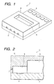
- Fig. 1 is a perspective view which schematically shows an ink jet recording head in accordance with one embodiment of the present invention.
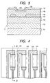
- Fig. 2 is a cross-sectional view which shows the ink jet recording head represented in Fig. 1, taken in the direction of liquid flow paths of the head schematically.
- the ink jet recording head 1 comprises an element substrate 2 provided with a plurality of heat generating devices 3 arranged in parallel (in Fig. 2, only one of them is shown) which generate thermal energy to be utilized for creating bubbles in ink, and a ceiling plate 4 which is bonded to the element substrate 2.
- a plurality of electrode pads 9 are arranged to receive electric signals from the outside in order to drive each of the heat generating devices 3.
- the element substrate 2 is a substrate having silicon material as its base.
- each of the liquid flow paths 5 is formed with each of the heat generating devices 3 correspondingly.
- a plurality of discharge ports 7 each communicated with each of the liquid flow paths 5, and an ink supply opening 8 through which ink is supplied from the outside to the common liquid chamber 6.
- Fig. 3 is a side sectional view which schematically shows the circumference of the heat generating portion of the element substrate of the ink jet recording head represented in Fig. 1.
- Fig. 4 is an upper end view which schematically shows the circumference of the heat generating portion of the element substrate of the ink jet recording head represented in Fig. 3.
- Fig. 3 is a side sectional view which schematically shows the corresponding portion, taken along one dot line 3-3 in Fig. 4.
- the thermally oxidized film 102 which serves as the heat accumulation layer
- the interlayer film 103 which is formed by silicon oxide (SiO 2 ) or silicon nitride (Si 3 N 4 ) and which dually serves as the heat accumulation layer.
- the heat generating resistive layer 104, and the wiring 105 formed by Al or Al alloy such as Al-Si or Al-Cu are patterned respectively.
- the protection layer 106 formed by silicon oxide (SiO 2 ) or silicon nitride (Si 3 N 4 ), and also, the cavitation proof film 107 formed by Ta to protect the protection film 106 from the chemical and physical shocks following the heat generation of the resistive layer 104.
- the region on the heat generating resistive layer 104 where the wiring 105 is not formed that is, the heat generating resistive layer 104 between the wirings 105 which serve as a pair of electrodes, is arranged to function as each of the heat generating devices.
- a reference numeral 108 designates the thermal activating portion where heat acts upon ink.
- each of the layers is formed on the silicon substrate by means of the semiconductor manufacture technologies and techniques to constitute the substrate for use of an ink jet recording head.
- the heat generating resistive layer 104 is structured to contain TaN 0.8,hex .
- the manufactured heat generating resistive layers, each containing TaN 0.8,hex presents smaller variations in its property, and even if a number of heat generating devices 3 are formed on one and the same substrate, its function is stabilized, and, further, the resistance changes are smaller even when its operational condition may change. Therefore, with such functional stability of a number of heat generating devices 3, it is possible to enable each of them to demonstrate the same effect in operation.
- Fig. 5 is a side sectional view schematically showing the element substrate of the ink jet recording head represented in Fig. 3, which is cut vertically.
- the impurity installation such as ion plantation and its diffusion are conducted to form the p-MOS on the n-type well region 402 of the silicon substrate 401, which is p conductor, and the n-MOS 451 on the p-type well region 403, respectively.
- the p-MOS 450 and the n-MOS 451 comprise the gate wiring 415, the source region 405 where the n-type or p-type impurity is implanted, the drain region 406, and some others, which are formed by polysilicon deposited by means of the CVD method in a thickness of 4,000 ⁇ or more and 5,000 ⁇ or less through the gate insulation film 408 of several hundreds ⁇ , respectively.
- the C-MOS logic is constructed by these p-MOS and n-MOS.
- the n-MOS transistor is arranged for use of element driving, which comprises the drain region 411, the source region 412, the gate wiring 413, and others formed also by the process of impurity installation and diffusion or the like.
- the distance L between drain and gate that form one transistor is 10 ⁇ m minimum approximately. This 10 ⁇ m breaks down as follows.
- the Al electrode 417 which is the contact of the source and drain, is 2 x 2 ⁇ m. In practice, however, a half of this contact is shared by the adjacent transistor. Therefore, it is a half of 2 x 2 ⁇ m.
- the gate wiring 413 is also 4 ⁇ m. The total thus makes 10 ⁇ m.
- the oxidized film separation region 453 is formed by means of the field oxidation in a thickness of 5,000 ⁇ to 10,000 ⁇ to separate each of the elements, respectively.
- the field oxidation film functions as the first heat accumulation layer 414 for the thermal activating portion 108.
- the interlayer insulation film 416 formed by PSG (Phospho-Silicate Glass) film, BPSG (Boron-Doped Phospho-Silicate Glass) film, or the like, prepared by the CVD method in a thickness of approximately 7,000 ⁇ . Further, subsequent to the smoothing process or the like that has been executed by heat treatment on the interlayer insulation film 416, wiring is made through the contact hole on the first wiring layer 417 formed by the Al electrodes. Then, the interlayer insulation film 418, which is formed by SiO 2 film or the like prepared in a thickness of 10,000 ⁇ to 15,000 ⁇ , is installed by plasma CVD.
- PSG Phospho-Silicate Glass
- BPSG Bioron-Doped Phospho-Silicate Glass
- the resistive layer 104 which is formed by TaN 0.8,hex film prepared in a thickness of approximately 1,000 ⁇ , is installed by DC sputtering method.
- This resistive layer 104 is partly in contact with the first wiring layer 417 by way of the through hole.
- the second wiring layer is formed with Al electrodes to serve as wiring to each of the heat generating devices.
- the protection film 106 which is formed by Si 3 N 4 film prepared in a thickness of approximately 10,000 ⁇ , is installed by the application of plasma CVD method.
- the cavitation proof film 107 is deposited with Ta or the like in a thickness of approximately 2,500 ⁇ .
- fluororesin film is formed as the water-repellent film 109.
- fluoroalkyl silane CF 3 (CF 2 ) 5 (CH 2 ) 2 Si(OMe) 3
- this compound is diluted with this compound being given as 1, isopropyl alcohol as 50, and nitric acid as 1, and dropped onto a glass Petri dish.
- the film is formed in a thickness of approximately 500 ⁇ by the application of CVD method at the room temperature.
- the contact angle of this water-repellent film with ink is 110°.
- resist is patterned by means of photolithography or the like on the portions other than the heat activating portion and the circumference thereof before the water-repellent film is formed. Then, the water-repellent material is applied to the entire surface. After that, the patterned water-repellent film is formed by the application of lift-off method for peeling off the resist.
- the patterned water-repellent film is formed by the application of lift-off method for peeling off the resist.
- the solvent dilution is conducted for the present embodiment.
- it may be possible to form the film in the plasmic atmosphere after having vaporized fluroroalkyl trimethoxylane (Rf-Si (OCH 3 ) 3 .RF CF 3 (CF 2 ) 7 CH 2 CH 2 ) in vacuum, for example. In this manner, a water-repellent film is formed with the Rf-Si group being bound in network.
- the ceiling plate 4 shown in Fig. 1 and Fig. 2 is positioned to face the element substrate 2 so that the grooves which form the liquid flow paths 5 are allowed to be in agreement with the heat generating devices 3, respectively, and then, bonded to complete the ink jet recording head 1.
- the water-repellent film is formed by the application of CVD method.
- the water-repellent film 109 may be formed by means of resin coating.
- the formation method of the water-repellent film 109 using resin coating there is a method whereby to coat the fluoropolymer film, which has the structure of fluorohetero ring in it, only the thermal activating portion in a thickness of 2,000 ⁇ by the application of spin coating method.
- the fluororesin "Cytop CTX-105" (product name: manufactured by Asahi Glass K.K.), "AF 1600" (product name: manufactured by Du Pont Inc.), or “Teflon AF" (product name: Du Pont Inc.) may be cited.
- the contact angle of this water-repellent film with ink is 100°.
- resist is patterned by means of photolithography or the like on the portions other than the thermal activating portion and the circumference thereof before the formation of the water-repellent film, and then, the water-repellent material is provided for the entire surface. After that, by means of the lift-off method for peeling off the resist, the patterned water-repellent film is formed.
- the patterned water-repellent film it may be possible to form the patterned water-repellent film with patterning subsequent to having formed the water-repellent material on the entire surface of the protection film 106.
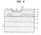
- Fig. 6 is a side sectional view which schematically shows the circumference of the heat activating portion of the element substrate of an ink jet recording head in accordance with the present embodiment.
- fluorine atom is implanted in the cavitation proof film 107 formed by Ta.
- the fluorine atom is induced into the ion source as gaseous compound and ionized by the application of electronic beam.
- the ion which is accelerated by use of the high voltage supply-source of approximately 100 kV, is selected by the mass spectrograph.
- fluorine atom is implanted in a unit of 1.0 x 10 14 to 1.0 x 10 16 atoms/cm 2 . After that, resist is removed.
- the fluorine atom thus implanted at high velocity is caused to elastically collide with Ta atom in the cavitation proof film 107 or it is decelerated by Coulomb's mutual action with electron. Since fluorine atom is comparatively light, this atom penetrates into the crystalline surface of Ta lightly. In order to allow fluorine atom to be stably at rest on the Ta surface by the application of thermal diffusion, the annealing process is executed for 10 to 100 minutes at 300°C to 500°C.
- the water-repellent surface which is formed with the crystal structure having fluorine atom, is arranged only on the heat generating portion.
- the contact angle of this water-repellent surface with ink is 90°.
- the ceiling plate 4 shown in Fig. 1 and Fig. 2 is positioned to face the element substrate 2 so that the grooves which form the liquid flow paths 5 are allowed to be in agreement with the heat generating devices 3, respectively, and then, bonded to complete the ink jet recording head 1.
- the material for the ceiling plate described in each of the above embodiments it is preferable to use polysulfone (contact angle with ink: 60°), silicon (contact angle with ink: 70°), glass (contact angle with ink: 70°), or the like.
- the contact angle with ink of the cavitation proof film 107 formed by Ta is approximately 60°, for example.
- the contact angle with ink slightly changes depending on the kinds of ink or the like, each value mentioned in each of the above embodiments is such as measured by use of ink whose surface tension is 30 dyn/cm.
- the ink which is retained temporarily in the common liquid chamber 6 after being supplied from the ink supply opening 8 to it, is caused to enter each of the liquid flow paths 5 by means of the capillary phenomenon, and from meniscus at each of the discharge ports 7, thus keeping each of the liquid flow paths 5 filled with ink.
- the heat generating devices 3 if each of the heat generating devices 3 is energized through the corresponding electrodes to generate heat, ink on each heat generating devices 3 is abruptly heated to create bubble in the corresponding liquid flow paths 5 by means of film boiling thus exerted. With the development of this bubble, ink is discharged from each of the discharge ports 7, respectively.
- colorant or compound contained in ink is decomposed at the molecular level when heated by each of the heat generating devices 3 to produce refractory substances in some cases. Since the water-repellent film 109 is formed on the uppermost layer of the thermal activating portion 108 that constitutes each of the heat generating devices 3, such refractory substances can hardly be fixed firmly on each of them irrespective of the kinds of ink to be used. Therefore, even when the heat is used for a long time, the heat conversion efficiency is not easily lowered, and the heat thus generated by each of the heat generating devices 3 is transferred to ink evenly to make it possible to stabilize the creation of bubbles and the development thereof as well. As a result, it becomes possible to attain the stable ink discharges.
- Fig. 7 is a perspective view which schematically shows one example of the principal part of the ink jet recording apparatus in accordance with the present invention.
- the lead screw 552 provided with a spiral groove 553 cut around it is axially supported on the main body frame 551 rotatively. Interlocked with the regular and reverse rotations of a driving motor 559, the lead screw 552 is driven to rotate through the driving power transmission gears 560 and 561. Further, the guide rail 554, which guides the carriage 555 slidably, is fixed to the main body frame 551.
- a pin (not shown) that engages with the spiral groove 553 is provided, and the carriage 555 reciprocates in the directions indicated by arrows a and b when the lead screw 552 rotates following the rotation of the driving motor 559.
- the sheet pressure plate 572 is arranged to press a recording medium 590 on the platen roller 573 over the direction in which the carriage 555 travels.
- an ink jet recording head cartridge 580 is mounted on the carriage 555.
- the ink jet recording head cartridge 580 is formed with the ink jet recording head described above which is formed integrally with an ink tank.
- the ink jet recording head cartridge 580 is supported on the carriage 555 fixedly by use of positioning means and electric contacts provided for the carriage 555. At the same time, this cartridge is arranged to be detachably mountable on the carriage 555.
- Photocoupler 557 and 558 constitute home position detecting means to confirm the presence of the lever 556 of the carriage 555 in this region and cause the driving motor 559 to rotate regularly or reversely, among some other operations.
- the cap member 567 that caps the front end (the surface where discharge ports are open) of the ink jet recording head is supported by the supporting member 562, and provided with suction means 566.
- the cap member executes the suction recovery of the ink jet recording head through the aperture 564 in the cap 568.
- a supporting plate 565 is fixed, and the cleaning blade 563, which is slidably supported by this supporting plate 565, is made movable in the forward and backward directions by driving means (not shown).
- the configuration of the cleaning blade 563 is not necessarily limited to the one shown in Fig. 7. It is of course possible to adopt any one of know cleaning blades.
- the lever 570 is arranged to initiate the suction recovery operation of the ink jet recording head. The lever moves along with the movement of the cam 571 which abuts upon the carriage 555, and its movement is controlled by use of the known transmission means such as a clutch or gears, which switches over the driving power from the driving motor 559 as required.
- Each process of these capping, cleaning, and suction recovery operations is executed in the respective positions correspondingly by the function of the lead screw 552 when the carriage 555 arrives in the region on the home position side. If only these operations are made executable as desired at the known timing, any types of arrangement may be adoptable for the present embodiment.
- the ink jet recording apparatus described above is provided with recording signal supply means for supplying recording signals to the ink jet recording head in order to drive the electrothermal converting members of the ink jet recording head mounted on the apparatus.
- the ink jet recording apparatus is also provided with a controller that controls the operations thereof.
- the ink jet recording apparatus of the present embodiment mounts on it the ink jet recording head described above, it is possible to implement the operation thereof with the stabilized ink discharges to attain the provision of images whose quality is rarely degraded.
- the example is shown, in which the ink jet recording head cartridge 580 is detachably mounted on the carriage 555.
- the present invention is not necessarily limited thereto.
- the structure may be such that the ink jet recording head is installed on the carriage 555, while only the ink tank is made detachably mountable on it.
Landscapes
- Engineering & Computer Science (AREA)
- Manufacturing & Machinery (AREA)
- Particle Formation And Scattering Control In Inkjet Printers (AREA)
Claims (14)
- Substrat (2) zum Gebrauch eines Tintenstrahldruckkopfs (1) mit Tintenpfaden (5), die mit Tintenauslassöffnungen (7) zum Auslassen von Tinte in Verbindung sind, mit:gekennzeichnet durchWärmeerzeugungsabschnitten (3), die an den Innenwandflächen der Tintenpfade (5) angeordnet sind, um thermische Energie zu erzeugen, die zum Auslassen von Tinte von den Auslassöffnungen (7) verwendet wird,
eine flüssigkeitsabweisende Behandlung (109), die an den Regionen durchgeführt wurde, die den Wärmeerzeugungsabschnitten (3) der Innenwandflächen der Tintenpfade (5) entsprechen, wobei die den Wärmeerzeugungsabschnitten (3) entsprechenden Regionen, die flüssigkeitsabweisend behandelt sind, die lediglich Bereich der Innenwandflächen der Tintenpfade (5) sind, die sich in Projektion auf die Flächen der Wärmeerzeugungswiderstandschicht (104) zwischen dem Paar Elektroden (105) und unmittelbar daneben angeordneten Abschnitten befinden. - Substrat (2) zum Gebrauch eines Tintenstrahldruckkopfs (1) gemäß Anspruch 1, wobei die Innenwandflächen der Tintenpfade (5) mit Ausnahme der den Wärmeerzeugungsabschnitten (3) entsprechenden Regionen lyophil sind.
- Substrat (2) zum Gebrauch eines Tintenstrahldruckkopfs (1) gemäß Anspruch 1, wobei die den Wärmeerzeugungsabschnitten (3) entsprechenden Regionen auf der obersten Schicht einer Vielzahl von für die Wärmeerzeugungsabschnitte (3) vorgesehenen Schutzschichten ausgebildet sind.
- Substrat (2) zum Gebrauch eines Tintenstrahldruckkopfs (1) gemäß Anspruch 3, wobei die oberste Lage eine Schicht ist, die Tantal enthält.
- Substrat (2) zum Gebrauch eines Tintenstrahldruckkopfs (1) gemäß Anspruch 1, wobei mit Hilfe der flüssigkeitsabweisenden Behandlung eine organische Schicht ausgebildet wird.
- Substrat (2) zum Gebrauch eines Tintenstrahldruckkopfs (1) gemäß Anspruch 1, wobei die flüssigkeitsabweisende Behandlung ein Prozess ist, bei dem Fluor verwendet wird.
- Substrat (2) zum Gebrauch eines Tintenstrahldruckkopfs (1) gemäß Anspruch 1, wobei die flüssigkeitsabweisende Behandlung ein Prozess ist, um den Kontaktwinkel mit Tinte 80° oder größer zu machen.
- Substrat (2) zum Gebrauch eines Tintenstrahldruckkopfs (1) gemäß Anspruch 7, wobei die flüssigkeitsabweisende Behandlung ein Prozess ist, um den Kontaktwinkel mit Tinte 100° oder größer zu machen.
- Substrat (2) zum Gebrauch eines Tintenstrahldruckkopfs (1) gemäß Anspruch 1, wobei die Dicke des mit der flüssigkeitsabweisenden Behandlung vorgesehenen Schicht 5000 Å oder weniger beträgt.
- Substrat (2) zum Gebrauch eines Tintenstrahldruckkopfs (1) gemäß Anspruch 1, wobei an dem Elementsubstrat, das die Wärmeerzeugungsabschnitte (3) darauf angeordnet hat, funktionale Vorrichtungen ausgebildet sind, um die Wärmeerzeugungsabschnitt (3) anzutreiben.
- Tintenstrahldruckkopf (1) mit einem Substrat (2) gemäß einem der Ansprüche 1 bis 10.
- Tintenstrahlkartusche (580) mit:einem Tintenstrahldruckkopf (1) gemäß Anspruch 11, undeinem Tintentank zum Aufnehmen von zu dem Tintenstrahldruckkopf (1) zuzuführender Tinte.
- Tintenstrahldruckgerät mit:wobei das Drucken ausgeführt wird, indem von dem Tintenstrahldruckkopf Tinte in Übereinstimmung mit den Drucksignalen ausgelassen wird.einem Tintenstrahldruckkopf gemäß Anspruch 11, undeiner Einrichtung zum Zuführen von Drucksignalen zum Zuführen von Drucksignalen, um den Tintenstrahldruckkopf anzutreiben,
- Tintenstrahldruckgerät mit:wobei das Drucken durchgeführt wird, indem Tinte von dem Tintenstrahldruckkopf in Übereinstimmung mit Drucksignalen ausgelassen wird.Halteeinrichtungen zum abnehmbaren Halten der Tintenstrahlkartusche gemäß Anspruch 12, undEinrichtungen zum Zuführen von Drucksignalen zum Zuführen von Drucksignalen, um den Tintenstrahldruckkopf anzutreiben,
Applications Claiming Priority (2)
| Application Number | Priority Date | Filing Date | Title |
|---|---|---|---|
| JP35345097 | 1997-12-22 | ||
| JP35345097 | 1997-12-22 |
Publications (3)
| Publication Number | Publication Date |
|---|---|
| EP0924080A2 EP0924080A2 (de) | 1999-06-23 |
| EP0924080A3 EP0924080A3 (de) | 2000-01-12 |
| EP0924080B1 true EP0924080B1 (de) | 2005-10-12 |
Family
ID=18430938
Family Applications (1)
| Application Number | Title | Priority Date | Filing Date |
|---|---|---|---|
| EP98124319A Expired - Lifetime EP0924080B1 (de) | 1997-12-22 | 1998-12-21 | Substrat für Tintenstrahlaufzeichnungskopf |
Country Status (3)
| Country | Link |
|---|---|
| US (1) | US6142606A (de) |
| EP (1) | EP0924080B1 (de) |
| DE (1) | DE69831849T2 (de) |
Families Citing this family (11)
| Publication number | Priority date | Publication date | Assignee | Title |
|---|---|---|---|---|
| US6345881B1 (en) * | 1999-09-29 | 2002-02-12 | Eastman Kodak Company | Coating of printhead nozzle plate |
| US6472125B1 (en) | 1999-11-30 | 2002-10-29 | Canon Kabushiki Kaisha | Method for manufacturing ink jet recording head and ink jet recording head manufactured by such method of manufacture |
| JP4282043B2 (ja) | 1999-12-06 | 2009-06-17 | キヤノン株式会社 | 記録液体供給通路、記録液体収納容器、およびこれらを備える記録液体供給装置、並びにその表面改質方法 |
| JP4125069B2 (ja) | 2002-08-13 | 2008-07-23 | キヤノン株式会社 | インクジェット記録ヘッド用基板、インクジェット記録ヘッドおよび該インクジェット記録ヘッドを用いたインクジェット記録装置 |
| JP4537246B2 (ja) * | 2004-05-06 | 2010-09-01 | キヤノン株式会社 | インクジェット記録ヘッド用基体の製造方法及び該方法により製造された前記基体を用いた記録ヘッドの製造方法 |
| US8227043B2 (en) * | 2004-06-28 | 2012-07-24 | Canon Kabushiki Kaisha | Liquid discharge head manufacturing method, and liquid discharge head obtained using this method |
| JP4459037B2 (ja) * | 2004-12-01 | 2010-04-28 | キヤノン株式会社 | 液体吐出ヘッド |
| JP4103009B2 (ja) * | 2005-03-23 | 2008-06-18 | セイコーエプソン株式会社 | 液滴吐出装置、およびマイクロアレイ製造方法 |
| WO2007105801A1 (ja) * | 2006-03-10 | 2007-09-20 | Canon Kabushiki Kaisha | 液体吐出ヘッド基体、その基体を用いた液体吐出ヘッドおよびそれらの製造方法 |
| US10035346B2 (en) * | 2015-01-27 | 2018-07-31 | Canon Kabushiki Kaisha | Element substrate and liquid ejection head |
| JP6598658B2 (ja) * | 2015-01-27 | 2019-10-30 | キヤノン株式会社 | 液体吐出ヘッドの素子基板及び液体吐出ヘッド |
Family Cites Families (12)
| Publication number | Priority date | Publication date | Assignee | Title |
|---|---|---|---|---|
| JPS5689569A (en) * | 1979-12-19 | 1981-07-20 | Canon Inc | Ink jet recording head |
| JPS5772868A (en) * | 1980-10-23 | 1982-05-07 | Canon Inc | Liquid injecting recording apparatus |
| JPS5772867A (en) * | 1980-10-23 | 1982-05-07 | Canon Inc | Liquid injecting recording apparatus |
| JPH0613219B2 (ja) * | 1983-04-30 | 1994-02-23 | キヤノン株式会社 | インクジェットヘッド |
| DE3446968A1 (de) * | 1983-12-26 | 1985-07-04 | Canon K.K., Tokio/Tokyo | Fluessigkeitsstrahlaufzeichnungskopf |
| JPS60159060A (ja) * | 1984-01-31 | 1985-08-20 | Canon Inc | 液体噴射記録ヘツド |
| JPS61193861A (ja) * | 1985-02-22 | 1986-08-28 | Nec Corp | インクジエツトヘツド |
| WO1991014575A1 (fr) * | 1990-03-27 | 1991-10-03 | Canon Kabushiki Kaisha | Tete enregistreuse a injection de liquide |
| JP2780844B2 (ja) * | 1990-04-28 | 1998-07-30 | キヤノン株式会社 | インクジェット記録ヘッド用基体、該基体を有するインクジェット記録ヘッド及び該記録ヘッドを備えたインクジェット記録装置 |
| JP2882487B2 (ja) * | 1990-04-28 | 1999-04-12 | キヤノン株式会社 | インクジェット記録ヘッド及び該記録ヘッドを備えたインクジェット記録装置 |
| JP2818003B2 (ja) * | 1990-04-28 | 1998-10-30 | キヤノン株式会社 | インクジェット記録ヘッド及び該記録ヘッドを備えたインクジェット記録装置 |
| US5729261A (en) * | 1996-03-28 | 1998-03-17 | Xerox Corporation | Thermal ink jet printhead with improved ink resistance |
-
1998
- 1998-12-17 US US09/215,740 patent/US6142606A/en not_active Expired - Lifetime
- 1998-12-21 DE DE69831849T patent/DE69831849T2/de not_active Expired - Lifetime
- 1998-12-21 EP EP98124319A patent/EP0924080B1/de not_active Expired - Lifetime
Also Published As
| Publication number | Publication date |
|---|---|
| DE69831849D1 (de) | 2006-02-23 |
| EP0924080A3 (de) | 2000-01-12 |
| EP0924080A2 (de) | 1999-06-23 |
| US6142606A (en) | 2000-11-07 |
| DE69831849T2 (de) | 2006-07-13 |
Similar Documents
| Publication | Publication Date | Title |
|---|---|---|
| US8491087B2 (en) | Circuit board for ink jet head, ink jet head having the same, method for cleaning the head and ink jet printing apparatus using the head | |
| US7980656B2 (en) | Liquid ejection head | |
| US6142606A (en) | Ink jet recording head, substrate for use of such head, ink jet cartridge, and ink jet recording apparatus | |
| US6719408B2 (en) | Liquid ejecting head, head cartridge, and liquid ejecting and recording apparatus | |
| US6464342B1 (en) | Liquid discharge head, head cartridge mounted on liquid discharge head and liquid discharge apparatus, and method for manufacturing liquid discharge head | |
| US6382775B1 (en) | Liquid ejecting printing head, production method thereof and production method for base body employed for liquid ejecting printing head | |
| EP0956953B1 (de) | Verfahren zur Herstellung eines Flüssigkeitsausstosskopfes | |
| US6799839B2 (en) | Structure provided with through hole, method of manufacture therefor, and liquid discharge head | |
| US6454379B1 (en) | Liquid discharge head and liquid discharge apparatus that uses the liquid discharge head, and discharge volume correction method for the liquid discharge head | |
| US7018020B2 (en) | Structure with through hole, production method thereof, and liquid discharge head | |
| JPH11240156A (ja) | インクジェット記録ヘッド、該インクジェット記録ヘッド用基体、インクジェットカートリッジおよびインクジェット記録装置 | |
| US20020130927A1 (en) | Substrate for use of ink jet head, ink jet head, and ink jet apparatus | |
| KR20050039625A (ko) | 액체 토출 헤드, 액체 토출 장치 및 액체 토출 헤드의제조 방법 | |
| JP3647316B2 (ja) | 液体吐出ヘッド及び該液体吐出ヘッドを用いた液体吐出装置 | |
| JPH11300977A (ja) | 液体吐出ヘッドの製造方法、液体吐出ヘッド、ヘッドカートリッジ及び液体吐出装置 | |
| JP2000141663A (ja) | 液体吐出ヘッド、液体吐出方法及び液体吐出装置 | |
| JP3710282B2 (ja) | 液体吐出ヘッドの製造方法、液体吐出ヘッド、該液体吐出ヘッドが搭載されたヘッドカートリッジおよび液体吐出装置 | |
| JPH11240157A (ja) | インクジェット記録ヘッド、該ヘッド用基板、該基板の製造方法及びインクジェット記録装置 | |
| JP3173811B2 (ja) | インクジェット記録ヘッド用基体およびインクジェット記録ヘッドの製造方法 | |
| JPH11300972A (ja) | 液体吐出ヘッド、ヘッドカートリッジ、液体吐出記録装置、および液体吐出ヘッドの製造方法 | |
| JP2000006414A (ja) | インクジェット記録ヘッド及び該ヘッドを用いたインクジェット記録装置 | |
| JP2003145767A (ja) | 液体吐出ヘッド、その製造方法及び液体吐出装置 | |
| JPH0596731A (ja) | 記録ヘツド用基体および記録ヘツドの製造方法 | |
| JP2005035234A (ja) | 液体吐出ヘッド、液体吐出装置及び液体吐出ヘッドの製造方法 | |
| JP2002307681A (ja) | 液体吐出ヘッドおよび液体吐出ヘッドの製造方法 |
Legal Events
| Date | Code | Title | Description |
|---|---|---|---|
| PUAI | Public reference made under article 153(3) epc to a published international application that has entered the european phase |
Free format text: ORIGINAL CODE: 0009012 |
|
| AK | Designated contracting states |
Kind code of ref document: A2 Designated state(s): DE ES FR GB IT NL |
|
| AX | Request for extension of the european patent |
Free format text: AL;LT;LV;MK;RO;SI |
|
| PUAL | Search report despatched |
Free format text: ORIGINAL CODE: 0009013 |
|
| AK | Designated contracting states |
Kind code of ref document: A3 Designated state(s): AT BE CH CY DE DK ES FI FR GB GR IE IT LI LU MC NL PT SE |
|
| AX | Request for extension of the european patent |
Free format text: AL;LT;LV;MK;RO;SI |
|
| RIC1 | Information provided on ipc code assigned before grant |
Free format text: 7B 41J 2/16 A, 7B 41J 2/14 B |
|
| 17P | Request for examination filed |
Effective date: 20000605 |
|
| AKX | Designation fees paid |
Free format text: DE ES FR GB IT NL |
|
| 17Q | First examination report despatched |
Effective date: 20020612 |
|
| GRAP | Despatch of communication of intention to grant a patent |
Free format text: ORIGINAL CODE: EPIDOSNIGR1 |
|
| RTI1 | Title (correction) |
Free format text: SUBSTRATE FOR USE IN AN INK JET RECORDING HEAD |
|
| GRAS | Grant fee paid |
Free format text: ORIGINAL CODE: EPIDOSNIGR3 |
|
| GRAA | (expected) grant |
Free format text: ORIGINAL CODE: 0009210 |
|
| AK | Designated contracting states |
Kind code of ref document: B1 Designated state(s): DE ES FR GB IT NL |
|
| PG25 | Lapsed in a contracting state [announced via postgrant information from national office to epo] |
Ref country code: NL Free format text: LAPSE BECAUSE OF FAILURE TO SUBMIT A TRANSLATION OF THE DESCRIPTION OR TO PAY THE FEE WITHIN THE PRESCRIBED TIME-LIMIT Effective date: 20051012 |
|
| REG | Reference to a national code |
Ref country code: GB Ref legal event code: FG4D |
|
| PG25 | Lapsed in a contracting state [announced via postgrant information from national office to epo] |
Ref country code: ES Free format text: LAPSE BECAUSE OF FAILURE TO SUBMIT A TRANSLATION OF THE DESCRIPTION OR TO PAY THE FEE WITHIN THE PRESCRIBED TIME-LIMIT Effective date: 20060123 |
|
| REF | Corresponds to: |
Ref document number: 69831849 Country of ref document: DE Date of ref document: 20060223 Kind code of ref document: P |
|
| NLV1 | Nl: lapsed or annulled due to failure to fulfill the requirements of art. 29p and 29m of the patents act | ||
| PLBE | No opposition filed within time limit |
Free format text: ORIGINAL CODE: 0009261 |
|
| STAA | Information on the status of an ep patent application or granted ep patent |
Free format text: STATUS: NO OPPOSITION FILED WITHIN TIME LIMIT |
|
| 26N | No opposition filed |
Effective date: 20060713 |
|
| PG25 | Lapsed in a contracting state [announced via postgrant information from national office to epo] |
Ref country code: FR Free format text: LAPSE BECAUSE OF FAILURE TO SUBMIT A TRANSLATION OF THE DESCRIPTION OR TO PAY THE FEE WITHIN THE PRESCRIBED TIME-LIMIT Effective date: 20061020 |
|
| EN | Fr: translation not filed | ||
| PG25 | Lapsed in a contracting state [announced via postgrant information from national office to epo] |
Ref country code: FR Free format text: LAPSE BECAUSE OF FAILURE TO SUBMIT A TRANSLATION OF THE DESCRIPTION OR TO PAY THE FEE WITHIN THE PRESCRIBED TIME-LIMIT Effective date: 20051231 |
|
| PG25 | Lapsed in a contracting state [announced via postgrant information from national office to epo] |
Ref country code: FR Free format text: LAPSE BECAUSE OF FAILURE TO SUBMIT A TRANSLATION OF THE DESCRIPTION OR TO PAY THE FEE WITHIN THE PRESCRIBED TIME-LIMIT Effective date: 20051012 |
|
| PGFP | Annual fee paid to national office [announced via postgrant information from national office to epo] |
Ref country code: DE Payment date: 20141231 Year of fee payment: 17 Ref country code: GB Payment date: 20141222 Year of fee payment: 17 |
|
| PGFP | Annual fee paid to national office [announced via postgrant information from national office to epo] |
Ref country code: IT Payment date: 20141204 Year of fee payment: 17 |
|
| REG | Reference to a national code |
Ref country code: DE Ref legal event code: R119 Ref document number: 69831849 Country of ref document: DE |
|
| GBPC | Gb: european patent ceased through non-payment of renewal fee |
Effective date: 20151221 |
|
| PG25 | Lapsed in a contracting state [announced via postgrant information from national office to epo] |
Ref country code: GB Free format text: LAPSE BECAUSE OF NON-PAYMENT OF DUE FEES Effective date: 20151221 Ref country code: DE Free format text: LAPSE BECAUSE OF NON-PAYMENT OF DUE FEES Effective date: 20160701 |
|
| PG25 | Lapsed in a contracting state [announced via postgrant information from national office to epo] |
Ref country code: IT Free format text: LAPSE BECAUSE OF NON-PAYMENT OF DUE FEES Effective date: 20151221 |