EP0921718A2 - Artikelträger und Herstellungsverfahren - Google Patents
Artikelträger und Herstellungsverfahren Download PDFInfo
- Publication number
- EP0921718A2 EP0921718A2 EP98309909A EP98309909A EP0921718A2 EP 0921718 A2 EP0921718 A2 EP 0921718A2 EP 98309909 A EP98309909 A EP 98309909A EP 98309909 A EP98309909 A EP 98309909A EP 0921718 A2 EP0921718 A2 EP 0921718A2
- Authority
- EP
- European Patent Office
- Prior art keywords
- carrier
- tape
- mold
- sides
- Prior art date
- Legal status (The legal status is an assumption and is not a legal conclusion. Google has not performed a legal analysis and makes no representation as to the accuracy of the status listed.)
- Withdrawn
Links
Images


Classifications
-
- H—ELECTRICITY
- H05—ELECTRIC TECHNIQUES NOT OTHERWISE PROVIDED FOR
- H05K—PRINTED CIRCUITS; CASINGS OR CONSTRUCTIONAL DETAILS OF ELECTRIC APPARATUS; MANUFACTURE OF ASSEMBLAGES OF ELECTRICAL COMPONENTS
- H05K13/00—Apparatus or processes specially adapted for manufacturing or adjusting assemblages of electric components
- H05K13/0084—Containers and magazines for components, e.g. tube-like magazines
Definitions
- the invention pertains to product or component carriers. More particularly, the invention pertains to product or component carriers wherein product positioning details are formed on surfaces some of which are directly in contact with the respective product or component.
- embossed plastic carrier tapes for use with surface mount components such as semiconductors including integrated circuits, contact elements or discrete electrical elements such as capacitors and resistors to facilitate automatic handling, insertion and connection to printed circuit boards or other types of substrates is well-recognized.
- Embossed carrier tapes are fabricated to meet standardized requirements with respect, for example, to leader characteristics, pitch, trailer characteristics and cover tape.
- Embossed carrier tapes are specified, for example, in 16 mm and 24 mm sizes in the March, 1991, Standard, EIA-481-2 entitled “16 mm and 24 mm Embossed Carrier Taping of Surface Mount Components for Automatic Handling”.
- Other tapes are specified in EIA-481-3 November of 1991, entitled “32 mm, 44 mm and 56 mm Embossed Carrier Taping of Surface Mount Components for Automatic Handling”.
- EIA-481-1-A, August, 1994, entitled "8 mm and & 12 mm Punched & Embossed Carrier Taping of Surface Mount Components for Automatic Handling” specifies yet other tape sizes.
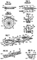
- Figs. 1 through 6 illustrate various deficiencies of known prior art approaches.
- Figs. 1, 2 and 4 illustrate two different prior art carrier tapes.
- Figs. 3 and 5 illustrate molds used to form the types of carrier tapes illustrated in Figs. 1, 2 and 4 and in particular that of Fig. 4.
- Fig. 6 illustrates another form of a prior art mold usable to form tapes of a type illustrated in Fig. 4.
- a prior art two-part molding system includes an upper or cover portion P1 and a lower or detail portion P2.
- the cover portion P1 is shown in Fig. 3 at a slight angle only for purposes of discussing the operation and characteristics thereof.
- the elements P1, P2 would exhibit relative linear motion toward and away form one another during the manufacturing process.
- the elements P1 and P2 cooperate to mold or emboss carrier tape T1, using a known prior art approach.
- Carrier tape T1 is initially a planar flexible thermal plastic tape of a predetermined width and thickness which is positioned between elements P1 and P2 after having been heated to an appropriate temperature. Once the mold elements P1 and P2 are brought together with a section of the carrier tape T1 therebetween, air pressure can be injected via hose H1 into the cavity C1. The air pressure in the cavity C1 forces the portion of the carrier tape T1 between elements P1 and P2 into the pocket defining female molds M1, M2, M3 and M4. This, in turn, forms a plurality of carrier pockets CP1, .. CP4 in the respective region of the tape T1.
- the component carrying pocket for example CPi of Fig. 4 is formed with much less detail or definition due to not having direct contact with the mold cavities M1 .. M4.
- the lack of direct contact by the mold element with the component positioning surfaces being formed limits the tolerances and precision to which those surfaces can be formed. The fact that the tolerances can not be reduced as needed for smaller parts limits the prior art technology.
- the thermal plastic material which makes up the tape T1 stretches. This, in turn, thins the walls of the cavity CPi and introduces wall thickness variations, which are not always of a predictable nature, into the respective cavity.
- each of the pockets formed in the carrier tape suffers from a loss of definition due to an absence of direct contact with the respective mold cavity in the block P2.
- Those pockets also suffer from variable wall thicknesses brought about by the molding process which may be of an unpredictable and random nature. Further, these variations are on the side of the component pocket where it is most desirable to hold the closest tolerances since it is that side of the pocket which ultimately determines the location of the product or component being carried on the tape.
- Rotary molds illustrated in Fig. 6, are also known in the prior art.
- female cavities R1-1, R1-2 .. R1-n, corresponding to the cavities M1 .. M4 of element P2 were formed in a rotary mold element such as element R1.
- Carrier tape T2 would be fed across the mold element R1 at a predetermined rate, consistent with the speed of rotation of the element R1.
- L1 either compressed air can be driven against the adjacent region of the tape T2 using fixture F1 and/or the respective cavity R1-i currently at the location L1 can be evacuated using evacuation conduit E1 to thereupon force-draw the relevant region of the tape T2 into the respective cavity.
- the rotary mold R1 as was the case with the linear mold combination P1, P2 imparts all of the detail of the respective cavity to the outside surfaces of the component carrying pocket being formed, comparable to that pocket illustrated in Fig. 4.
- carrier tape on the order of .016 inches thick can be embossed using air pressure in a range of 39 to 100 psi and molds of the general type illustrated in Figs. 3 and 6. This process results in component carrier pockets wherein positioning tolerances can only be held to within ⁇ .005 inches.
- molds and methods which can be used to produce molded carrier tape to smaller tolerances than has heretofore been possible using the prior art approaches.
- molds and methods can be configured so as to minimize in-pocket variations due to variable wall thicknesses.
- carrier tapes could be manufactured in a way that light incident thereon will be dispersed instead of reflected. Suppression of such reflections is desirable in scanning or optical monitoring systems which can used to check product or component location and contact arrangement in the carrier pocket.
- a product carrier can be formed in a flexible planar plastic member by molding or embossing a product receiving pocket into the member.
- the pocket includes at least one product positioning surface formed in the pocket. The pocket and the surface are formed in response to corresponding surface of a male mold element engaging and deflecting a respective portion of the planar member.
- the male mold element carries product positioning detail which is imparted to the shape of the pocket being formed by bring i ng the male mold element into contact with one side of the respective region of the tape. In this fashion, all of the component or product positioning detail is imparted directly into surfaces formed within the pocket.
- fluid pressure can be applied against the other side of the carrier tape forcing it against the male mold element to more accurately and more faithfully conform the interior surface of the pocket to the exterior surface of the male mold.
- one or more channels can be formed in the male mold. As the carrier tape is being forced around and formed to the male mold, a vacuum can be drawn via the conduit. The low pressure produced by the vacuum creates a greater pressure differential relative to air pressure on the other side of the carrier tape thereby further improving the conformity between the interior of the pocket and the adjacent male mold.
- surfaces on or adjacent to the male mold element can be interrupted by a predetermined pattern, such as cross hatching or corrugations or undulations. These patterns can in turn be transferred to the adjacent regions of the carrier tape and the respective pocket during the molding process. Hence, the finished carrier tape exits the mold not only with detailed product positioning surfaces formed therein but also carrying light dispersing patterns which can be expected to improve the performance of scanning or optical monitoring systems.
- the mold can be formed with multiple spaced apart pocket defining male mold elements. At the end of each molding step wherein a plurality of pockets can be formed at the same time, the mold elements can be withdrawn from the tape and the tape moved to the next position so that the next group of pockets can be formed.
- a rotary mold which carries a plurality if radially extending male mold elements can be used.
- the carrier tape is wound in part around the rotating multi-element mold.
- the tape moves with the rotary mold and at the appropriate station or stations, either fluid under pressure can be injected against the carrier tape thereby driving it against a respective male mold element and/or a conduit or path extending through the mold element can be evacuated thereby increasing a pressure differential against the tape.
- a pressure differential against the tape As a result, the pocket being formed in the region of the tape is brought into greater conformity with the shape of the male mold element.
- an axially extending trough can be formed in an embossed tape relative to an upper or seal surface.
- Spaced apart product positioning features or surfaces can be formed along the trough.
- discrete component carrying pockets are not formed. Instead, the product positioning features preclude axial or lateral component movement relative to the tape. Pocket walls are not needed.
- a seal or cover tape, adhesively attached to the seal surface holds components on the positioning features.
- the trough can be interrupted by embossed laterally extending features or elements between pairs of component positioning features. These laterally extending elements help minimize kinking or distortion as the tape is coiled onto a reel.
- Fig. 7 illustrates an embossed carrier tape 10 in accordance with the present invention.
- the tape 10 as illustrated includes a plurality of different component carrying pockets 12a, 12b .. 12e.
- the pocket 12a .. 12e of the tape 10 are illustrated having different shapes for purposes of explaining the present invention.
- the pockets of the tape 10 are intended to carry, for example, connection pins that are to be automatically inserted into an electronic product.
- Each of the pockets, such as 12a is formed by deflecting a respective surface region of the surface 10-1 of the tape 10 as described below.
- each of the pockets, such as 12a has a respective extension surface, such as 12'a, formed from a respective region of the second surface 10-2.
- the carrier tape 10 is formed from a standard planar, elongated flexible thermal plastic tape.
- the component carrying pockets 12a .. 12e of the tape 10 exhibit lower tolerance characteristics wherein parts can be positioned repeatedly within ⁇ .001 inches.
- light diffusing patterns can be molded into the tape 10 on the product carrying side for purposes of improving the performance of scanning or optical monitoring systems.
- Fig. 8 illustrates a sectional view of pocket 12a with an exemplary connection pin PN of a first orientation to be carried therein.
- the pocket 12a exhibits an internal component carrying pocket surface 14a which includes a product positioning boring and support surface 14b.
- the exemplary tape 10 is intended to be used to carry small electronic connector pins.
- Each pin PN is carried in a separate pocket with a selected orientation.
- the boring and positioning surface 14b would be intended to position and carry the discrete connector pin PN.
- the component carrying pocket 14a is bounded by planar regions 14e, f.
- the regions 14e, f as discussed subsequently, have a thickness corresponding to that of an unprocessed tape.
- Fig. 9 illustrates an alternate form of a pocket 12c.
- the pocket 12c is intended to position and carry the same type of pin PN as was carried by the pocket 12a. However, for illustrative purposes the pin PN is shown with a different orientation in Fig. 9.
- the pocket 12c includes an interior surface 16a, an exterior surface 12'c and a pin receiving and support region 16b.
- the pocket 12c a as illustrated in Fig. 9 includes first and second planar bounding regions 16e, 16 f. Additionally, the pocket 16a includes first and second spaced apart linear depressions 16g, 16h. These depressions provide an elevated support for the positioning surface and boring 16b which receives the pin PN. As a result of the elevation of the region 16b, the part PN does not extend beyond a common terminating surface indicated generally at 16i.
- Fig. 10 and 11 illustrate another carrier 20 in accordance with the present invention but for a different type of a component.
- the carrier tape 20 is formed of a plurality of substantially identical pockets such as 22i.
- the sectional view, Fig. 11, illustrates details of a representative one of the pockets 22i of the carrier tape 20.
- the pocket 22i includes a lower positioning feature or surface 22a, an adjacent pair of product positioning surfaces 22b, c and an upper positioning surface 22d generally parallel to the surface 22a. Spaced apart planar edge regions 22c, 22d bound the pocket 22i.
- a component such as contact element C 1 illustrated in phantom is received within the pocket 22i and positioned by the surfaces 22a . . 22d.
- the surfaces 22a .. 22d could assume a variety of configurations based on the shape of the particular component or portion thereof, such as connector leads, which are to be positioned for subsequent automatic assembly. It will be understood that the configuration of the component to be carried is not a limitation of the present invention.
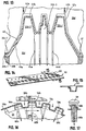
- Fig. 12 illustrates an exemplary multi-part mold system or assembly 30 usable for manufacturing the tape 10, for example.
- a similar mold assembly could be used, with elements having different shapes, to manufacture the tape 20.
- This system 30 includes three elements.
- Element 30a carries the detail, in the form of a male mold element to be formed into a component carrying pocket.
- 30b is a clamping ring which slideably receives the element 30a during the molding or embossing process.
- Element 30c illustrated at an angle in Fig. 12 for purposes of explanation only, carries a plurality of female mold cavities each of which is intended to mate with a respective one of the male mold elements from the element 30a during the molding process.
- the element 30a carries four different male molds, 32a .. 32d, for exemplary purposes only.
- the molds 32a.. 32d correspond to the interior shapes of the pockets 12a .. 12d.
- the clamping element 30b defined a plurality of identical spaced apart bores 34a .. 34d which slidably receive respective ones of the male elements 32a .. 32d.
- a planar clamping surface 30b-1 surrounds each of the bores 34a .. 34d.
- the element 30c carries a plurality of female molds 36a .. 36d which are intended to substantially conform to and mate with the male molds 32a .. 32d. As described subsequently, when so arranged, therein a predetermined space therebetween for the molded material which forms the respective pocket, such as 12a .. 12d.
- a planar clamping surface 30c-1 surrounds each of the cavities 36a .. 36d.
- a fluid pressure hose H1 extends from the female element 30c.
- An evacuation-hose H2 extends from the male element 30a.
- the carrier tape 10 is preheated to a predetermined temperature in the order of 325° - 340° F. prior to entering the mold station 30. With the elements 30a and 30c retracted, the tape 10 is positioned in the mold station 30 adjacent to the element 30b.
- the mold elements 30b, 30c are moved linearly relatively toward one another, for example by holding the element 30b fixed and moving the element 30c theretoward.
- the tape 10 is clamped therebetween by the surfaces 30b-1 and 30c-1.
- the tape 10 is still in a planar state.
- the mold element 30a is forced toward and into the surface 10-1 of the tape 10.
- Pneumatic or hydraulic actuators can be used. for example, pneumatic pressure on the order of 100 psi can be used.
- This relative movement of the element 30a toward the female mold element 30c drives each of the respective defining male extensions 32a, 32b, 32c, 32d into the tape 10 thereby deforming same in accordance with the surfaces on each of the respective male mold elements.
- the regions of the deforming tape 10 are driven into the respective female elements such as 36a, 36b .. 36d by the surfaces of the respective male mold elements 32a .. 32d.
- the adjacent planar regions of the carrier tape 10, such as 14c, 14f, are clamped between surfaces 30b-1 and 30c-1 and are held substantially stationary. This results in a stretching and a deforming of the portions of the carrier tape 10 which are bounded by the openings 34a .. 34d which are aligned with the female molds 36a .. 36d.
- the portions of the carrier 10 adjacent to each of the respective regions are forced by the respective male mold elements, such as the element 32a, into the respective female mold such as the mold 36a.
- External surfaces of the pocket 12a are in part formed by the respective female mold 36a.
- Fig. 13 Further details of the molding process are illustrated in Fig. 13. As illustrated in Fig. 13, with respect to the mold element 32d, the spacing between the male mold element 32d and the respective female cavity 36d is on the order .016 inches. This spacing corresponds to the thickness of the carrier tape 10 in its normal unembossed state. Hence, in the regions where the surfaces 30b-1 and 30c-1 clamp the tape 10, the spacing between those elements is in the order of .016 inches. The regions 10' of the carrier 10 which are trapped therebetween do not move appreciably during the embossing or molding process.
- the developing wall of the pocket 12c is stretched, deformed and thinned.
- the side wall thickness of the pocket 12c will be reduced from .016 inches to about .006-.007 inches leaving a gap 40 between the surface 12'c thereof and the female mold element 36d.
- Fluids such as air or hydraulic fluid can be injected into the gap 40 via conduits 42a, 42b coupled to hose H1 to apply pressure to the surface 12'c thereby forcing the respective portion of the carrier against the surfaces of the male mold element 32d thereby more closely replicating the features thereof.
- a vacuum can be drawn relative to the carrier tape material between the mold elements 32d and 36d. This increases the gradient or pressure different between the exterior surface 12'c of the pocket 12c thereupon further forcing the carrier tape material in the regions between the two mold elements against the male mold element 32d.
- pneumatic pressure is injected via the conduits 42a, 42b, air pressure on the order to 30-150 PSI can be used for the purpose of conforming the carrier tape material to the exterior surfaces of each of the male mold elements 32a .. 32d.
- the shape of the carrier pocket 12c is precisely defined by the features and surfaces of the male mold element 32d against which that material is forced.
- wall variations which may occur during the molding process, as illustrated by thicker wall region 46a and thinner wall regions 46b, will appear on the outer surface 12'c of the pocket.
- the variability of the wall thickness of the respective pocket which has now been translated to the outer surface thereof, has been eliminated as a source of variability of the position of the electronic component being carried by the molded pocket and boring 16b.
- product positioning detail can be molded into the component pocket with a tolerance in the order of ⁇ .001 inches.
- the mold system 30 can be configured with multiple pocket molds. For example, a four-element mold as is illustrated in Fig. 12, depending upon pitch, can generate up to 200 meters per hour of embossed tape.
- Figs. 14 and 15 illustrate a carrier structure 50 made in accordance with a rotary mold 56 as illustrated in Figs. 16 and 17.
- the carrier 50 is formed of a plurality of spaced apart component receiving pockets, for example pocket 50i.
- While the carrier 50 can be manufactured using mold system of the type illustrated in Figs. 12 and 13, it can alternately be manufactured using a rotary mold as illustrated in Fig. 16.
- the mold 56 of Fig 16 is formed with a plurality of angularly disposed, substantially identical, male mold elements 56a, b, c, d.
- a linear incoming carrier tape having a planar region 58a is drawn against the rotating mold 56 along a curve.
- the tape 58a which has been preheated is then forced against mold element 56b by fluid pressure 59 which could be either pneumatic, hydraulic at a work station thereby forming the respective component receiving pocket, such as 50i.
- the mold 56 can be provided with a plurality of evacuation channels 60a .. 60d whereby a vacuum can be applied to the interior of the pocket being formed by the mold element 56b in the region 58b thereby increasing a pressure differential between the exterior and interior size of the pocket. This differential in turn draws the carrier tape in the region 58b against the features and surfaces of the mold element 56b thereupon imparting the features of those surfaces to the inside of the respective component carrying pocket 50i.
- Fig. 18 illustrates a molding system usable for manufacturing product carrier tapes, such as the tape 20.
- the system 70 includes a tape feed reel 72 from which planar carrier tape 74 is fed.
- the tape 74 passes through a heating station indicated generally at 76. Subsequently it passes through a multiple unit molding station, which includes for example a mold system such as the mold system 30 in Fig. 12. Subsequent to leaving the molding station 30, the embossed or molded tape 20 is wound onto a take-up reel 78.
- a control element 80 coupled to the various components of the system 70 can be used to monitor and oversee system operation.
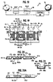
- Fig. 19 is a top plan view of yet another, carrier tape 84.
- the tape 84 is formed with a planar plastic upper or seal surface 86.
- Embossed in the seal surface 86 is a plurality of product receiving recesses or depressions 86-1, 86-2 .. 86-n.
- the embossed tape 84 could be formed using rotary mold 56 for example.
- a representative depression 86-2 in the tape 84 is defined by a bottom 87a and axially extending side regions 87b, c. Depression 86-2 is further defined by embossed, laterally extending ridges or shoulders 87d, e.
- the ridges or shoulders 87d, e are depressed relative to seal surface 86 (best seen in Fig. 20).
- the ridges 87d, c extend between pairs of component positioning elements such as 86-1a, 1b; 86-2a, 2b and 86-3a, 3b.
- a component C2 (see Fig. 24) might for example sit on top surfaces of 86-2a, 2b and have contacts that extend, in part, along front and back edges such as 86-2f, 2g.
- the top surfaces of 86-2a, 2b in combination with side surfaces such as 86-2f, 2g will thus lock C2 into a fixed position in depression 86-2.
- the spacing shoulders 87d, 87e are not intended to position C2.
- the lateral protrusions 87d, e are intended to facilitate coiling tape 84 in a reel such as the reel 78. The function to minimize kinking of the embossed tape.
- the tape 84 can be regarded in Fig. 19 as having been embossed with a continuously extending trough indicated generally at 84a.
- the trough 84a is interrupted by the depressed anti-kinking elements 87d, 87e and component spacing elements 86-2a, 2b.
- trough 84a' can be embossed into tape 84' without the laterally extending elements 87d, 87e. Tape 84' will then be coiled to minimize side-wall kinking even in the absence of the elements 87d, 87e.
- Component C2' (shown in phantom) is illustrated in Fig. 20A positioned on and held in place by elements 86-2a', 2b'.
- Each of the depressions 86-1 ... 86-n carries at least an embossed or molded light reflecting pattern 88a.
- the pattern 88a illustrated on the lower surface 87a of the respective carrier depression 86-1, 86-2 .. 86n, beneficially disperses and reduces reflections of light incident upon the respective depression or region of the carrier tape.
- undulating patterns can be molded into the side walls, such as the corrugated patterns 88b illustrated in Fig. 19. It will be understood that the patterns 88a, 88b can be used alone or in combination.
- the patterns 88a, 88b are imparted into the respective depressions in the trough 84a from the respective male mold elements.
- the undulations 88b not only deflect and diffuse reflected light, they also strengthen the respective pocket or trough side walls thereby minimizing kinking or distortion.
- patterns can be molded or embossed on upper and lower surfaces of the tape 84.
- Pattern 88c illustrated in Fig. 19 can be molded into the edge regions or seal surface 86 of the tape 84 or between carrier pockets, if desired.
- the pattern 88c is imparted to the tape 86 at a molding station from clamping surfaces such as the surfaces 30b-1 and 30c-1. The location and arrangement of the patterns on the respective surfaces 30b-1 and 30c-1 determines where those patterns are imparted to the tape 84.
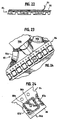
- the seal surface 86 can be roughened (indicated at 84b, Fig. 24) to improve adherence characteristics, as described subsequently, of an adhesively bonded cover tape 89.
- Fig. 22 illustrates the tape 84 with the adhesively attached cover tape 89, illustrated in a partly removed state.
- the removable cover tape 89 can be attached to seal surface 86. That surface in turn can carry patterns 88c or be abraded 84b or otherwise processed to produce a roughened or textured surface during or after the molding step. This processing in turn improves the adherability of the cover tape 89 to the seal surface 86.
- Fig. 23 illustrates a tape, such as the tape 84 which has been loaded with components C2, passing through a scanning or optical monitoring system 90.
- a scanning or optical monitoring system 90 Such systems typically include one or more sources of illumination 90a and an optical scanner 90b.
- a representative pocket which carries a component C2 also carries light diffusing patterns 88a and 88b for the purpose of minimizing reflections from sources 90a.
- Components C2 which register appropriately with the scanning system 90 can in turn be picked up and automatically assembled into a predetermined product.
Landscapes
- Engineering & Computer Science (AREA)
- Manufacturing & Machinery (AREA)
- Microelectronics & Electronic Packaging (AREA)
- Blow-Moulding Or Thermoforming Of Plastics Or The Like (AREA)
- Moulds For Moulding Plastics Or The Like (AREA)
- Packages (AREA)
- Casting Or Compression Moulding Of Plastics Or The Like (AREA)
Applications Claiming Priority (2)
| Application Number | Priority Date | Filing Date | Title |
|---|---|---|---|
| US985505 | 1997-12-05 | ||
| US08/985,505 US6003676A (en) | 1997-12-05 | 1997-12-05 | Product carrier and method of making same |
Publications (2)
| Publication Number | Publication Date |
|---|---|
| EP0921718A2 true EP0921718A2 (de) | 1999-06-09 |
| EP0921718A3 EP0921718A3 (de) | 2000-05-03 |
Family
ID=25531550
Family Applications (1)
| Application Number | Title | Priority Date | Filing Date |
|---|---|---|---|
| EP98309909A Withdrawn EP0921718A3 (de) | 1997-12-05 | 1998-12-03 | Artikelträger und Herstellungsverfahren |
Country Status (3)
| Country | Link |
|---|---|
| US (1) | US6003676A (de) |
| EP (1) | EP0921718A3 (de) |
| BR (1) | BR9816149A (de) |
Cited By (2)
| Publication number | Priority date | Publication date | Assignee | Title |
|---|---|---|---|---|
| WO2006078493A3 (en) * | 2005-01-20 | 2006-11-23 | 3M Innovative Properties Co | Component carrier and method for making |
| US8021628B2 (en) | 2005-01-20 | 2011-09-20 | 3M Innovatice Properties Company | Structured polymer films |
Families Citing this family (17)
| Publication number | Priority date | Publication date | Assignee | Title |
|---|---|---|---|---|
| DE10038163A1 (de) * | 2000-08-04 | 2002-02-14 | Infineon Technologies Ag | Vorrichtung und Verfahren zur Bestückung von Transportgurten |
| US6871394B2 (en) * | 2002-01-31 | 2005-03-29 | Texas Instruments Incorporated | Method for aligning substrates in a tray |
| US6966440B1 (en) * | 2002-08-12 | 2005-11-22 | Autosplice Systems, Inc. | Tape-packaged headed pin contact |
| JP4517856B2 (ja) * | 2004-12-27 | 2010-08-04 | Tdk株式会社 | 電子部品連 |
| EP1963198A1 (de) * | 2005-12-20 | 2008-09-03 | 3M Innovative Properties Company | Trägerband für teile |
| US7611016B2 (en) * | 2007-07-31 | 2009-11-03 | 3M Innovative Properties Company | Non-nesting component carrier tape |
| US8117725B2 (en) * | 2008-10-31 | 2012-02-21 | The Gillette Company | Method of manufacturing a plurality of molded components |
| US8205766B2 (en) * | 2009-05-20 | 2012-06-26 | The Bergquist Company | Method for packaging thermal interface materials |
| US8430264B2 (en) * | 2009-05-20 | 2013-04-30 | The Bergquist Company | Method for packaging thermal interface materials |
| US9090403B2 (en) * | 2011-12-16 | 2015-07-28 | 3M Innovative Properties Company | Carrier tape |
| JP5791532B2 (ja) * | 2012-01-31 | 2015-10-07 | 株式会社ソシオネクスト | 収容体及びリール |
| US8564012B2 (en) | 2012-02-10 | 2013-10-22 | Intersil Americas LLC | Optoelectronic apparatuses and methods for manufacturing optoelectronic apparatuses |
| US8796052B2 (en) | 2012-02-24 | 2014-08-05 | Intersil Americas LLC | Optoelectronic apparatuses with post-molded reflector cups and methods for manufacturing the same |
| JP5790633B2 (ja) * | 2012-12-14 | 2015-10-07 | 株式会社村田製作所 | キャリアテープ、包装用テープおよび電子部品連 |
| CN104308862B (zh) * | 2014-10-21 | 2016-07-06 | 太仓思比科微电子技术有限公司 | 一种可视化真空载具 |
| JP6904738B2 (ja) * | 2017-03-14 | 2021-07-21 | 能美防災株式会社 | エンボステープ |
| JPWO2023203955A1 (de) * | 2022-04-20 | 2023-10-26 |
Family Cites Families (45)
| Publication number | Priority date | Publication date | Assignee | Title |
|---|---|---|---|---|
| DE1155967B (de) * | 1961-08-01 | 1963-10-17 | Karl Lang K G Papierverarbeitu | Verfahren zur Herstellung einer Verpackungseinlage und Vorrichtung zu seiner Durchfuehrung |
| US3311229A (en) * | 1965-01-21 | 1967-03-28 | Nat Patent Dev Corp | Tablet package |
| US3465874A (en) * | 1967-06-12 | 1969-09-09 | Frances Hugle | Carrier for semiconductor devices |
| US3858721A (en) * | 1971-10-01 | 1975-01-07 | Western Electric Co | Loading of compliant tape |
| US3946864A (en) * | 1974-07-01 | 1976-03-30 | Hutson Jearld L | Semiconductor chip package |
| US4272473A (en) * | 1978-12-07 | 1981-06-09 | The Procter & Gamble Company | Method for embossing and perforating a running ribbon of thermoplastic film on a metallic pattern roll |
| JPS5827398A (ja) * | 1981-08-11 | 1983-02-18 | 松下電器産業株式会社 | 電子部品集合体 |
| JPS6092700A (ja) * | 1983-10-26 | 1985-05-24 | 株式会社東芝 | フラツトパツケ−ジ集積回路素子収納装置 |
| JPS60144298U (ja) * | 1984-03-05 | 1985-09-25 | 株式会社村田製作所 | チツプ型電子部品連 |
| US4564880A (en) * | 1984-03-14 | 1986-01-14 | Motorola, Inc. | Apparatus and method for protecting integrated circuits |
| JPS6151896A (ja) * | 1984-08-21 | 1986-03-14 | 株式会社村田製作所 | 電子部品連 |
| US4736841A (en) * | 1985-02-20 | 1988-04-12 | Murata Manufacturing Co., Ltd. | Electronic component series |
| NL8503063A (nl) * | 1985-11-08 | 1987-06-01 | Philips Nv | Bandverpakking voor elektrische en/of elektronische onderdelen. |
| US4819801A (en) * | 1988-01-11 | 1989-04-11 | Savoy Leather Manufacturing Corporation | Storage case |
| US5026303A (en) * | 1988-03-10 | 1991-06-25 | Yamaichi Electric Manufacturing Co., Ltd. | Slotless type IC carrier |
| JPH0219271A (ja) * | 1988-07-06 | 1990-01-23 | Toshiba Corp | 半導体装置用テーピング部品 |
| JPH0245368A (ja) * | 1988-07-23 | 1990-02-15 | Nec Corp | 半導体装置の包装用部材 |
| JPH0257576A (ja) * | 1988-08-12 | 1990-02-27 | Minnesota Mining & Mfg Co <3M> | 電子部品収納用テープ |
| US4966281A (en) * | 1988-09-09 | 1990-10-30 | Nitto Denko Corporation | Electronic component carrier |
| GB8825154D0 (en) * | 1988-10-27 | 1988-11-30 | Reel Service Ltd | Tape for storage of electronic components |
| JPH02127256A (ja) * | 1988-10-28 | 1990-05-15 | Hitachi Ltd | 電子部品搬送テープ |
| US4966282A (en) * | 1989-01-13 | 1990-10-30 | Nitto Denko Corporation | Electronic component carrier |
| US4898275A (en) * | 1989-05-25 | 1990-02-06 | Minnesota Mining And Manufacturing Company | Non nesting component carrier tape |
| US5101975A (en) * | 1990-10-31 | 1992-04-07 | Novapak, Inc. | Electronic component carrier |
| US5066245A (en) * | 1990-11-09 | 1991-11-19 | Amp Incorporated | Retention device for flat pack sockets |
| US5115911A (en) * | 1991-02-04 | 1992-05-26 | Illinois Tool Works Inc. | Carrier tape system |
| US5234104A (en) * | 1991-02-04 | 1993-08-10 | Illinois Tool Works Inc. | Carrier tape system |
| US5361901A (en) * | 1991-02-12 | 1994-11-08 | Minnesota Mining And Manufacturing Company | Carrier tape |
| US5132160A (en) * | 1991-02-21 | 1992-07-21 | Minnesota Mining And Manufacturing Company | Component carrier tape |
| US5265723A (en) * | 1992-09-30 | 1993-11-30 | Advantek, Inc. | Microchip storage tape and cover therefor |
| US5152393A (en) * | 1991-07-08 | 1992-10-06 | Advantek, Inc. | Microchip storage tape |
| US5226226A (en) * | 1991-07-29 | 1993-07-13 | Fierkens Richard H J | Tube-shaped package for a semiconductor device and method therefor |
| JPH0767932B2 (ja) * | 1991-09-13 | 1995-07-26 | 浦和ポリマー株式会社 | キャリアテープの製造方法 |
| US5259500A (en) * | 1991-12-23 | 1993-11-09 | Joseph Alvite | Tape packaging system with removeable covers |
| US5199564A (en) * | 1992-03-13 | 1993-04-06 | Minnesota Mining And Manufacturing Company | Carrier tape for electronic through-hole components |
| US5351821A (en) * | 1992-04-30 | 1994-10-04 | Minnesota Mining And Manufacturing Company | Carrier tape with generic pockets |
| US5396988A (en) * | 1992-04-30 | 1995-03-14 | Minnesota Mining And Manufacturing Company | Electronic component carrier tape with generic pockets |
| DE69303230D1 (de) * | 1992-05-13 | 1996-07-25 | Gold Ind Co Ltd | Verketteter Behälter zum Transportieren von Präzisionsvorrichtungen |
| US5390472A (en) * | 1992-06-19 | 1995-02-21 | Minnesota Mining And Manufacturing Company | Carrier tape with cover strip |
| JPH07101461A (ja) * | 1993-09-30 | 1995-04-18 | Yayoi Kk | エンボスキャリアテープ |
| US5447784A (en) * | 1994-06-01 | 1995-09-05 | Rexham Industries Corp. | Electrostatic dissipating cover tape |
| JPH08104306A (ja) * | 1994-09-30 | 1996-04-23 | Stanley Electric Co Ltd | キャリアエンボステーピング装置 |
| US5524765A (en) * | 1994-11-15 | 1996-06-11 | Tempo G | Carrier tape packaging system utilizing a layer of gel for retaining small components |
| US5526935A (en) * | 1995-02-15 | 1996-06-18 | Minnesota Mining And Manufacturing Company | Component carrier tape |
| US5664680A (en) * | 1996-04-09 | 1997-09-09 | Caritech Inc. | Pockets for microchip carriers |
-
1997
- 1997-12-05 US US08/985,505 patent/US6003676A/en not_active Expired - Lifetime
-
1998
- 1998-12-03 EP EP98309909A patent/EP0921718A3/de not_active Withdrawn
- 1998-12-07 BR BR9816149-0A patent/BR9816149A/pt not_active Application Discontinuation
Cited By (3)
| Publication number | Priority date | Publication date | Assignee | Title |
|---|---|---|---|---|
| WO2006078493A3 (en) * | 2005-01-20 | 2006-11-23 | 3M Innovative Properties Co | Component carrier and method for making |
| US8021628B2 (en) | 2005-01-20 | 2011-09-20 | 3M Innovatice Properties Company | Structured polymer films |
| US8173079B2 (en) | 2005-01-20 | 2012-05-08 | 3M Innovative Properties Company | Method for forming structured polymeric film |
Also Published As
| Publication number | Publication date |
|---|---|
| US6003676A (en) | 1999-12-21 |
| BR9816149A (pt) | 2002-06-25 |
| EP0921718A3 (de) | 2000-05-03 |
Similar Documents
| Publication | Publication Date | Title |
|---|---|---|
| EP0921718A2 (de) | Artikelträger und Herstellungsverfahren | |
| JP3971541B2 (ja) | 半導体装置の製造方法及びこの方法に用いる分割金型 | |
| KR20190135281A (ko) | 적층 코어 제조 장치 | |
| US7846290B2 (en) | Method and apparatus for manufacturing friction plate | |
| JP2772760B2 (ja) | 図柄付き合成樹脂フイルムの図柄拡大方法 | |
| WO2018038356A1 (ko) | 적층 코어의 내경 가열이 가능한 적층 코어 제조 장치 | |
| TW201603670A (zh) | 軟性印刷電路板之製造方法、電路板製造用夾具及電路板製造裝置 | |
| US5800772A (en) | Method for producing embossed carrier tape system | |
| CN113478703B (zh) | 一种四面曲立体光学纹理模芯制做方法 | |
| JP2851205B2 (ja) | 成形同時絵付け用金型と成形同時絵付け方法 | |
| CN112622320A (zh) | 一种层叠式保压盒组 | |
| CN118100492A (zh) | 空心杯电机用绕组线圈、成型方法、电机绕组和成型治具 | |
| JP3742806B2 (ja) | サングラス用偏光レンズの成形方法および成形装置 | |
| KR102358094B1 (ko) | 4d 프린팅 기술을 사용한 곡면형 성형품의 제조 방법 | |
| JP4132300B2 (ja) | エンボスキャリアテープ成形装置 | |
| CN217502206U (zh) | 保压治具及压合装置 | |
| CN214872615U (zh) | 圆形一体式载带成型模具 | |
| JP2610323B2 (ja) | 成形装置 | |
| JPH10321457A (ja) | セラミック積層部品の製造方法及び製造装置 | |
| CN221623141U (zh) | 包装盒成型设备 | |
| JP2004167726A (ja) | エンボスキャリアテープの製造方法、及び、エンボスキャリアテープ製造装置 | |
| JP3210216B2 (ja) | パネル保持装置と枠体付きパネルの製造方法 | |
| JP4248852B2 (ja) | 樹脂成形用金型 | |
| JP2542986B2 (ja) | 成形同時絵付け方法と成形同時絵付け用金型 | |
| KR20240125367A (ko) | 탄성체를 활용하여 단차가 형성된 측면을 가지는 필름을 제조하는 방법 및 시스템 |
Legal Events
| Date | Code | Title | Description |
|---|---|---|---|
| PUAI | Public reference made under article 153(3) epc to a published international application that has entered the european phase |
Free format text: ORIGINAL CODE: 0009012 |
|
| AK | Designated contracting states |
Kind code of ref document: A2 Designated state(s): AT BE DE FI FR GB IE NL SE |
|
| AX | Request for extension of the european patent |
Free format text: AL;LT;LV;MK;RO;SI |
|
| PUAL | Search report despatched |
Free format text: ORIGINAL CODE: 0009013 |
|
| AK | Designated contracting states |
Kind code of ref document: A3 Designated state(s): AT BE CH CY DE DK ES FI FR GB GR IE IT LI LU MC NL PT SE |
|
| AX | Request for extension of the european patent |
Free format text: AL;LT;LV;MK;RO;SI |
|
| RIC1 | Information provided on ipc code assigned before grant |
Free format text: 7H 05K 13/00 A, 7H 05K 13/04 B |
|
| 17P | Request for examination filed |
Effective date: 20001002 |
|
| AKX | Designation fees paid |
Free format text: AT BE DE FI FR GB IE NL SE |
|
| 17Q | First examination report despatched |
Effective date: 20060116 |
|
| STAA | Information on the status of an ep patent application or granted ep patent |
Free format text: STATUS: THE APPLICATION IS DEEMED TO BE WITHDRAWN |
|
| 18D | Application deemed to be withdrawn |
Effective date: 20070724 |