EP0917196A2 - Halbleiterelementmodul und Halbleiter - Google Patents
Halbleiterelementmodul und Halbleiter Download PDFInfo
- Publication number
- EP0917196A2 EP0917196A2 EP98116772A EP98116772A EP0917196A2 EP 0917196 A2 EP0917196 A2 EP 0917196A2 EP 98116772 A EP98116772 A EP 98116772A EP 98116772 A EP98116772 A EP 98116772A EP 0917196 A2 EP0917196 A2 EP 0917196A2
- Authority
- EP
- European Patent Office
- Prior art keywords
- package
- leads
- semiconductor element
- substrate
- element module
- Prior art date
- Legal status (The legal status is an assumption and is not a legal conclusion. Google has not performed a legal analysis and makes no representation as to the accuracy of the status listed.)
- Granted
Links
Images


Classifications
-
- H—ELECTRICITY
- H05—ELECTRIC TECHNIQUES NOT OTHERWISE PROVIDED FOR
- H05K—PRINTED CIRCUITS; CASINGS OR CONSTRUCTIONAL DETAILS OF ELECTRIC APPARATUS; MANUFACTURE OF ASSEMBLAGES OF ELECTRICAL COMPONENTS
- H05K3/00—Apparatus or processes for manufacturing printed circuits
- H05K3/30—Assembling printed circuits with electric components, e.g. with resistors
- H05K3/32—Assembling printed circuits with electric components, e.g. with resistors electrically connecting electric components or wires to printed circuits
- H05K3/34—Assembling printed circuits with electric components, e.g. with resistors electrically connecting electric components or wires to printed circuits by soldering
- H05K3/3447—Lead-in-hole components
-
- H—ELECTRICITY
- H05—ELECTRIC TECHNIQUES NOT OTHERWISE PROVIDED FOR
- H05K—PRINTED CIRCUITS; CASINGS OR CONSTRUCTIONAL DETAILS OF ELECTRIC APPARATUS; MANUFACTURE OF ASSEMBLAGES OF ELECTRICAL COMPONENTS
- H05K3/00—Apparatus or processes for manufacturing printed circuits
- H05K3/30—Assembling printed circuits with electric components, e.g. with resistors
- H05K3/32—Assembling printed circuits with electric components, e.g. with resistors electrically connecting electric components or wires to printed circuits
- H05K3/34—Assembling printed circuits with electric components, e.g. with resistors electrically connecting electric components or wires to printed circuits by soldering
- H05K3/341—Surface mounted components
- H05K3/3421—Leaded components
- H05K3/3426—Leaded components characterised by the leads
-
- H—ELECTRICITY
- H10—SEMICONDUCTOR DEVICES; ELECTRIC SOLID-STATE DEVICES NOT OTHERWISE PROVIDED FOR
- H10W—GENERIC PACKAGES, INTERCONNECTIONS, CONNECTORS OR OTHER CONSTRUCTIONAL DETAILS OF DEVICES COVERED BY CLASS H10
- H10W70/00—Package substrates; Interposers; Redistribution layers [RDL]
- H10W70/40—Leadframes
- H10W70/481—Leadframes for devices being provided for in groups H10D8/00 - H10D48/00
-
- H—ELECTRICITY
- H05—ELECTRIC TECHNIQUES NOT OTHERWISE PROVIDED FOR
- H05K—PRINTED CIRCUITS; CASINGS OR CONSTRUCTIONAL DETAILS OF ELECTRIC APPARATUS; MANUFACTURE OF ASSEMBLAGES OF ELECTRICAL COMPONENTS
- H05K2201/00—Indexing scheme relating to printed circuits covered by H05K1/00
- H05K2201/10—Details of components or other objects attached to or integrated in a printed circuit board
- H05K2201/10431—Details of mounted components
- H05K2201/10568—Integral adaptations of a component or an auxiliary PCB for mounting, e.g. integral spacer element
-
- H—ELECTRICITY
- H05—ELECTRIC TECHNIQUES NOT OTHERWISE PROVIDED FOR
- H05K—PRINTED CIRCUITS; CASINGS OR CONSTRUCTIONAL DETAILS OF ELECTRIC APPARATUS; MANUFACTURE OF ASSEMBLAGES OF ELECTRICAL COMPONENTS
- H05K2201/00—Indexing scheme relating to printed circuits covered by H05K1/00
- H05K2201/10—Details of components or other objects attached to or integrated in a printed circuit board
- H05K2201/10613—Details of electrical connections of non-printed components, e.g. special leads
- H05K2201/10621—Components characterised by their electrical contacts
- H05K2201/10689—Leaded Integrated Circuit [IC] package, e.g. dual-in-line [DIL]
-
- H—ELECTRICITY
- H05—ELECTRIC TECHNIQUES NOT OTHERWISE PROVIDED FOR
- H05K—PRINTED CIRCUITS; CASINGS OR CONSTRUCTIONAL DETAILS OF ELECTRIC APPARATUS; MANUFACTURE OF ASSEMBLAGES OF ELECTRICAL COMPONENTS
- H05K3/00—Apparatus or processes for manufacturing printed circuits
- H05K3/30—Assembling printed circuits with electric components, e.g. with resistors
- H05K3/303—Assembling printed circuits with electric components, e.g. with resistors with surface mounted components
-
- H—ELECTRICITY
- H05—ELECTRIC TECHNIQUES NOT OTHERWISE PROVIDED FOR
- H05K—PRINTED CIRCUITS; CASINGS OR CONSTRUCTIONAL DETAILS OF ELECTRIC APPARATUS; MANUFACTURE OF ASSEMBLAGES OF ELECTRICAL COMPONENTS
- H05K3/00—Apparatus or processes for manufacturing printed circuits
- H05K3/30—Assembling printed circuits with electric components, e.g. with resistors
- H05K3/306—Assembling printed circuits with electric components, e.g. with resistors with lead-in-hole components
-
- H—ELECTRICITY
- H10—SEMICONDUCTOR DEVICES; ELECTRIC SOLID-STATE DEVICES NOT OTHERWISE PROVIDED FOR
- H10W—GENERIC PACKAGES, INTERCONNECTIONS, CONNECTORS OR OTHER CONSTRUCTIONAL DETAILS OF DEVICES COVERED BY CLASS H10
- H10W90/00—Package configurations
- H10W90/701—Package configurations characterised by the relative positions of pads or connectors relative to package parts
- H10W90/751—Package configurations characterised by the relative positions of pads or connectors relative to package parts of bond wires
- H10W90/754—Package configurations characterised by the relative positions of pads or connectors relative to package parts of bond wires between a chip and a stacked insulating package substrate, interposer or RDL
-
- H—ELECTRICITY
- H10—SEMICONDUCTOR DEVICES; ELECTRIC SOLID-STATE DEVICES NOT OTHERWISE PROVIDED FOR
- H10W—GENERIC PACKAGES, INTERCONNECTIONS, CONNECTORS OR OTHER CONSTRUCTIONAL DETAILS OF DEVICES COVERED BY CLASS H10
- H10W90/00—Package configurations
- H10W90/701—Package configurations characterised by the relative positions of pads or connectors relative to package parts
- H10W90/751—Package configurations characterised by the relative positions of pads or connectors relative to package parts of bond wires
- H10W90/756—Package configurations characterised by the relative positions of pads or connectors relative to package parts of bond wires between a chip and a stacked lead frame, conducting package substrate or heat sink
-
- Y—GENERAL TAGGING OF NEW TECHNOLOGICAL DEVELOPMENTS; GENERAL TAGGING OF CROSS-SECTIONAL TECHNOLOGIES SPANNING OVER SEVERAL SECTIONS OF THE IPC; TECHNICAL SUBJECTS COVERED BY FORMER USPC CROSS-REFERENCE ART COLLECTIONS [XRACs] AND DIGESTS
- Y02—TECHNOLOGIES OR APPLICATIONS FOR MITIGATION OR ADAPTATION AGAINST CLIMATE CHANGE
- Y02P—CLIMATE CHANGE MITIGATION TECHNOLOGIES IN THE PRODUCTION OR PROCESSING OF GOODS
- Y02P70/00—Climate change mitigation technologies in the production process for final industrial or consumer products
- Y02P70/50—Manufacturing or production processes characterised by the final manufactured product
Definitions
- the present invention relates to a semiconductor element module and a semiconductor device.
- a semiconductor element is an optical element (light emitting element, light receiving element).
- Fig. 7A is a side view of a conventional semiconductor element module;
- Fig. 7B is a side view of Fig. 7A;
- Fig. 7C is a front view taken in line A - A' in Fig. 7A.
- reference numeral 1 denotes an optical element for converting an electric signal into an optical signal and vice versa; 2 an optical fiber for transmitting the optical signal; 3 a mount for adjusting/fixing the optical axes of the optical element 1 and optical fiber 2; 4 a package for hermetically sealing the optical element; 5 one of wires for connecting the optical element 1 and package 4; 6 one of leads, provided on both sides of the package 4 so that an opening end is oriented to the a package attaching plane, for connecting the optical element and external circuit; and 7 one of brazing materials for connecting the package and the leads 6.
- the wire 5 and leads 6 are electrically connected to each other through the package 4.
- FIG. 8A is a side view of a semiconductor device in which a conventional semiconductor element module is mounted on a substrate through through-holes formed in a substrate.
- Fig. 8B is a front view of Fig. 8A.
- reference numeral 8 denotes a substrate on which a semiconductor element module is mounted; 9 a solder for mounting; and 10 one of through-holes made in the substrate 8.
- Fig. 9A is a side view of a semiconductor device in which a conventional semiconductor element module is mounted on a substrate through conductor patterns formed on a mounting surface of the substrate.
- the conventional semiconductor element module and semiconductor device configured as described above has the following problems.
- the solder used for mounting solder material used to solder the leads 6 through the through-holes 10) is molten owing to heating so that a part of the molten solder flows into a slight gap formed between a package bottom and substrate 8 by a capillary phenomemon, thus short-circuiting the leads 6 to each other.
- the leads 6 when the semiconductor module is mounted on the substrate through the conductor patterns 11 mounted on the mounting surface of the substrate 8, the leads 6 must be shaped at a portion apart from the brazing materials 7 in order to maintain the connecting strength between the package 4 and leads 6. Since the brazing materials 7 are located at a position near the bottom of the package, in order to satisfy the above requirement, the leads 6 will be shaped (outward bending) at a portion thereof apart from the package bottom. This increases the height of the semiconductor device after mounting.
- the present invention has been accomplished in order to solve the above problem, and intends to provide a semiconductor element module and a semiconductor device which can prevent solder for mounting from flowing into a slight gap formed between a package bottom and a substrate by a capillary phenomenon when the semiconductor element module is mounted on the substrate through through-holes formed therein, thus preventing the leads from being short-circuited with each other.
- the leads When the semiconductor element module is mounted on a substrate through a conductor pattern provided on a mounting surface of the substrate, the leads must be shaped at positions apart from the brazing material so that the connecting strength between the package and leads are not attenuated.
- the brazing material is located at a position apart from the bottom of the package, the present invention intends to provide a semiconductor element module and a semiconductor device which permits the lead to be molded at a position near to the package bottom to lower the height after mounting.
- the semiconductor element module according to the first invention is structured so that a level differences is provided on the side of the package attaching plane of each of package sides so that a space is formed from each the plurality of leads.
- the semiconductor device according to the second invention is structured to include a semiconductor element module according to the first invention and a substrate having conductor patterns and through-holes for connecting the conductor patterns to each other wherein each the leads is soldered to the substrate through each the though-holes so that the bottom of the package abuts on a mounting plane.
- the semiconductor device according to the third invention is structured so as to include a semiconductor element module according to the first invention and a substrate having conductor patterns for lead connection on a mounting plane thereof wherein each the leads is soldered to the substrate through each the conductor patterns so that the bottom of the package forms a prescribed space from the mounting plane.
- the semiconductor element module according to the fourth invention is structured to further include brazing materials for connecting the package and each the leads and so that the level difference forms a space permitting each the leads to be shaped at its portion near to the package.
- the semiconductor element module according to the fifth invention is structured so that the level difference formed in the first or fourth invention serves to prevent the short-circuiting between the leads adjacent to each other.
- the semiconductor element module according to the sixth invention is structured so that a level differences is provided at a portion of each the leads not connected to the package so that the width of each the leads on the side where the lead and package are connected is thick and that on the side of its opening end is thin.
- the semiconductor device according to the seventh invention is constructed to includes a semiconductor element module according to the sixth invention and a substrate having conductor patterns and through-holes for connecting the conductor patterns to each other wherein each the leads is soldered to the substrate through each the though-holes so that the level difference of each the leads abuts on a mounting plane of the substrate.
- the semiconductor device according to the eighth invention is structured so as to include a semiconductor element module according to the sixth invention and a substrate having conductor patterns for lead connection on a mounting plane thereof wherein each the leads is soldered to the substrate through each the conductor patterns so that the bottom of the package forms a prescribed space from the mounting plane of the substrate.
- the semiconductor element module according to the ninth invention is structured to further include brazing materials for connecting the package and each the leads and so that the level difference provides different mechanical strengths permitting each the leads to be shaped at its portion near to the package.
- the semiconductor element module according to the tenth invention is structured so that the level difference formed in the semiconductor element module according to the sixth or ninth invention serves to prevent the short-circuiting between the leads adjacent to each other.
- the semiconductor element module according to the eleventh invention is structured so that the semiconductor element is an optical element.
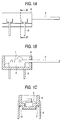
- Fig. 1A is a side view of the first embodiment of the invention; and Fig. 1B is a sectional view of Fig. 1A; Fig. 1A is a front view taken along line A - A' in Fig. 1A.
- reference numerals 1 - 7 refer to like parts in the conventional semiconductor module and semiconductor device.
- Reference numeral 12 denotes one of grooved level differences each forming a space between the lead 6 and the side of the package attaching plane of sides of the package.
- Fig. 2A is a side view showing a semiconductor device in which a semiconductor element module according to the present invention is mounted on a substrate through through-holes provided therein.
- Fig. 2B is a front view thereof.
- reference numerals 1 to 10 refer to like parts in the conventional semiconductor element module and semiconductor device shown in Fig. 8.
- the package 4 is soldered to the substrate 8 through the through-holes 10 so that its bottom abuts on the mounting plane.
- the grooved level difference 12 is formed so that the bottom of the package 4 is not brought into contact with the conductor pattern formed on the periphery of the through-holes and solder used for mounting, when the leads 6 are soldered through the through-holes 10, a part of molten solder will not flow into the slight gap formed between the package bottom and substrate by the capillary phenomenon and hence the leads will not be short-circuited with each other.
- Fig. 3A is a side view of a semiconductor device in which a semiconductor element module according to the present invention is mounted on a substrate through a conductor pattern formed on a mounting plane of the substrate.
- Fig. 3B is a front view thereof.
- reference numerals 1 - 9 and 11 refer to like parts in the conventional semiconductor element module and semiconductor device shown in Fig. 9.
- Reference numeral 12 corresponds to the grooved level differences shown in Figs. 1A to 1C and 2A, 2B.
- the package 4 is soldered to the substrate 8 through the conductor pattern so that its bottom forms a prescribed space from a mounting plane of the substrate.
- the brazing material 7 is located apart from the package bottom.
- the lead can be bent outwardly at a portion thereof near to the package bottom.
- the package can be mounted without attenuating the connecting strength between the package 4 and the lead.
- the height of the semiconductor device after mounting can be lowered compared with the conventional semiconductor device.
- Fig. 4A is a side view showing the third embodiment according to the present invention.
- Fig. 4B is a sectional view of Fig. 4A.
- Fig. 4C is a front view taken in line A - A' of Fig. 4A.
- reference numerals 1 to 7 refer to like parts of the conventional element module and semiconductor device.
- Reference numeral 13 denotes one of lead level differences, provided at a portion of the lead 6 not connected to the package 4 so that the side where the lead 6 and the package 4 are connected is thick while the side of the opening end is thin.
- Fig. 5A is a side view of a semiconductor device in which the semiconductor element module is mounted on the substrate through through-holes therein.
- Fig. 5B is a front view thereof.
- reference numerals 1 to 10 refer to like parts of the conventional semiconductor element module and semiconductor device shown in Figs. 7 and 8.
- the above lead level difference 13 is provided so that its width on the side where the lead 6 and package 4 are connected is larger than the hole diameter of the through-hole 10 and that on the side of its opening end is smaller than that of the through-hole 10.
- the package 4 is soldered to the substrate 8 through the through-holes 10 so that the level difference of the lead 6 abuts on the mounting plane.
- the lead level difference 13 is formed at the portion of the lead 6 not connected to the package 4 so that the bottom of the package 4 is not brought into contact with the conductor pattern formed on the periphery of the through-holes and solder for the lead and through-hole used for mounting.
- Fig. 6A is a side view showing a semiconductor device in which a semiconductor module according to the present invention is mounted on a substrate through a conductor patterns formed therein.
- Fig. 6B is a front view thereof.
- reference numerals 1 to 9 and 11 refer to like parts of the conventional element module and semiconductor device shown in Fig. 9.
- Reference numeral 13 denotes one of lead level differences similar to that in Figs. 4A to 4C and 5A, 5B.
- the package 4 is soldered to the substrate through the conductor patterns 11 so that its bottom forms a prescribed space with a mounting plane (i.e. upper surface of the substrate 8).
- the lead level difference 13 is formed to provide different mechanical strengths according to the diameter of the lead.
- the package 4 can be mounted on the substrate without attenuating the connecting strength between the package 4 and lead 6, thereby decreasing the height after mounting as compared with the case in the prior art.
- first and third embodiments an explanation will be separately given of the case where the lead is soldered to the substrate 8 through the through-hole 10 formed therein (first and third embodiments), and the case where the lead 6 is soldered to the substrate 8 through the conductor pattern (second and fourth embodiment).
- the semiconductor device can provide a more excellent high frequency characteristic.
- the lead(s) requiring the high frequency characteristic may be soldered through the conductor pattern provided on the mounting plane of the substrate while the remaining lead(s) may be soldered through the through-hole located on the substrate to position the semiconductor element module, thus providing the same effect.
- the semiconductor element is an optical element
- the semiconductor element may be an IC to provide the same effect.
- a semiconductor element module and a semiconductor device can be provided which can prevent solder used for mounting from flowing in between the bottom of the package and substrate when the semiconductor element module is mounted on the substrate through the through-holes formed therein.
- a semiconductor element module and a semiconductor device can be provided which can lower the height after mounting when the semiconductor element module is mounted on the substrate through the conductor patterns provided on the mounting plane of the substrate.
Landscapes
- Engineering & Computer Science (AREA)
- Manufacturing & Machinery (AREA)
- Microelectronics & Electronic Packaging (AREA)
- Structures For Mounting Electric Components On Printed Circuit Boards (AREA)
- Optical Couplings Of Light Guides (AREA)
- Lead Frames For Integrated Circuits (AREA)
- Light Receiving Elements (AREA)
Applications Claiming Priority (3)
| Application Number | Priority Date | Filing Date | Title |
|---|---|---|---|
| JP31526097 | 1997-11-17 | ||
| JP315260/97 | 1997-11-17 | ||
| JP31526097A JP3374732B2 (ja) | 1997-11-17 | 1997-11-17 | 半導体素子モジュールおよび半導体装置 |
Publications (3)
| Publication Number | Publication Date |
|---|---|
| EP0917196A2 true EP0917196A2 (de) | 1999-05-19 |
| EP0917196A3 EP0917196A3 (de) | 2003-01-08 |
| EP0917196B1 EP0917196B1 (de) | 2008-03-05 |
Family
ID=18063300
Family Applications (1)
| Application Number | Title | Priority Date | Filing Date |
|---|---|---|---|
| EP98116772A Expired - Lifetime EP0917196B1 (de) | 1997-11-17 | 1998-09-04 | Halbleiterelementmodul und Halbleiter |
Country Status (4)
| Country | Link |
|---|---|
| US (1) | US5986337A (de) |
| EP (1) | EP0917196B1 (de) |
| JP (1) | JP3374732B2 (de) |
| DE (1) | DE69839205T2 (de) |
Cited By (1)
| Publication number | Priority date | Publication date | Assignee | Title |
|---|---|---|---|---|
| EP1320112A1 (de) * | 2001-12-11 | 2003-06-18 | Yazaki Corporation | Relaisvorrichtung und Befestigungsstruktur |
Family Cites Families (20)
| Publication number | Priority date | Publication date | Assignee | Title |
|---|---|---|---|---|
| JPS5758469A (en) * | 1980-09-26 | 1982-04-08 | Hitachi Ltd | Solid-state image sensor |
| EP0218022B1 (de) * | 1985-08-14 | 1992-07-29 | OMRON Corporation | Montagestruktur für einen oberflächenmontierten Bauelementtyp und Verfahren zum Montieren dieses Bauelementtyps auf einer Leiterplatte |
| JPH07120730B2 (ja) * | 1986-01-13 | 1995-12-20 | イビデン 株式会社 | 電子部品を搭載した樹脂基板 |
| US4890152A (en) * | 1986-02-14 | 1989-12-26 | Matsushita Electric Works, Ltd. | Plastic molded chip carrier package and method of fabricating the same |
| DE3780764T2 (de) * | 1986-11-15 | 1992-12-24 | Matsushita Electric Works Ltd | Gegossenes kunststoff-chip-gehaeuse mit steckermuster. |
| JPS63174344A (ja) * | 1987-01-14 | 1988-07-18 | Matsushita Electric Works Ltd | ピングリツドアレイ |
| JPS6439051A (en) * | 1987-08-05 | 1989-02-09 | Matsushita Electric Works Ltd | Pin grid array |
| JPS6460542A (en) * | 1987-08-28 | 1989-03-07 | Hitachi Ltd | Paper conveying tractor mechanism |
| US4890154A (en) * | 1988-03-02 | 1989-12-26 | Lsi Logic Corporation | Semiconductor package profile |
| JPH0229538A (ja) * | 1988-04-14 | 1990-01-31 | Mitsubishi Electric Corp | 空気調和機の制御装置 |
| JPH01307251A (ja) * | 1988-06-03 | 1989-12-12 | Fujitsu Ltd | 表面実装型パッケージ |
| JPH0212861A (ja) * | 1988-06-30 | 1990-01-17 | Nec Corp | 樹脂封止型半導体装置 |
| US5231305A (en) * | 1990-03-19 | 1993-07-27 | Texas Instruments Incorporated | Ceramic bonding bridge |
| JP2721748B2 (ja) * | 1990-10-09 | 1998-03-04 | 三菱重工業株式会社 | Ic用メタルパッケージ |
| JPH04199556A (ja) * | 1990-10-30 | 1992-07-20 | Mitsubishi Electric Corp | ピングリッドアレイ形icパッケージ |
| JPH05102348A (ja) * | 1991-10-04 | 1993-04-23 | Seiko Epson Corp | 半導体装置 |
| JPH05144962A (ja) * | 1991-11-21 | 1993-06-11 | Kyocera Corp | プラグイン型半導体素子収納用パツケージ |
| JPH05218269A (ja) * | 1992-02-03 | 1993-08-27 | Fujitsu Ltd | 半導体装置 |
| JP3093476B2 (ja) * | 1992-08-31 | 2000-10-03 | ローム株式会社 | 電子部品およびその実装方法 |
| US5567984A (en) * | 1994-12-08 | 1996-10-22 | International Business Machines Corporation | Process for fabricating an electronic circuit package |
-
1997
- 1997-11-17 JP JP31526097A patent/JP3374732B2/ja not_active Expired - Lifetime
-
1998
- 1998-08-24 US US09/138,562 patent/US5986337A/en not_active Expired - Lifetime
- 1998-09-04 EP EP98116772A patent/EP0917196B1/de not_active Expired - Lifetime
- 1998-09-04 DE DE69839205T patent/DE69839205T2/de not_active Expired - Lifetime
Cited By (2)
| Publication number | Priority date | Publication date | Assignee | Title |
|---|---|---|---|---|
| EP1320112A1 (de) * | 2001-12-11 | 2003-06-18 | Yazaki Corporation | Relaisvorrichtung und Befestigungsstruktur |
| US6924964B2 (en) | 2001-12-11 | 2005-08-02 | Yazaki Corporation | Relay device and relay device mounting structure |
Also Published As
| Publication number | Publication date |
|---|---|
| JPH11150200A (ja) | 1999-06-02 |
| DE69839205D1 (de) | 2008-04-17 |
| US5986337A (en) | 1999-11-16 |
| JP3374732B2 (ja) | 2003-02-10 |
| EP0917196B1 (de) | 2008-03-05 |
| EP0917196A3 (de) | 2003-01-08 |
| DE69839205T2 (de) | 2009-03-12 |
Similar Documents
| Publication | Publication Date | Title |
|---|---|---|
| US5712767A (en) | Circuit elements mounting | |
| US7170151B2 (en) | Accurate alignment of an LED assembly | |
| US5057805A (en) | Microwave semiconductor device | |
| US5723900A (en) | Resin mold type semiconductor device | |
| US4951124A (en) | Semiconductor device | |
| US4949225A (en) | Circuit board for mounting electronic components | |
| US6344682B1 (en) | Semiconductor device comprising a semiconductor element mounted on a substrate and covered by a wiring board | |
| US6332720B1 (en) | Semiconductor laser coupling device and method for assembling the same on circuit board | |
| US9588313B2 (en) | Optical device package and optical device apparatus | |
| US5398166A (en) | Electronic component and mounting structure thereof | |
| US6833512B2 (en) | Substrate board structure | |
| US5986337A (en) | Semiconductor element module and semiconductor device which prevents short circuiting | |
| US5294749A (en) | Surface mountable molded electronic component | |
| US5442134A (en) | Lead structure of semiconductor device | |
| JP2005165165A (ja) | レセプタクル及びレセプタクルの製造方法 | |
| US6498294B1 (en) | Package for high frequency device | |
| US6787890B2 (en) | Optical package structure | |
| JP2000164970A (ja) | 光素子モジュール | |
| JPH09232709A (ja) | 回路基板装置 | |
| JP3726718B2 (ja) | 半導体装置 | |
| JP2001024143A (ja) | 複合半導体装置 | |
| JP4176217B2 (ja) | 多光軸光電スイッチの回路基板 | |
| KR100450797B1 (ko) | 광통신 모듈용 실리콘 광학 벤치 | |
| JPH11211940A (ja) | 光モジュール | |
| JP2009043909A (ja) | リモコン受光ユニットおよびこれを搭載した電子機器 |
Legal Events
| Date | Code | Title | Description |
|---|---|---|---|
| PUAI | Public reference made under article 153(3) epc to a published international application that has entered the european phase |
Free format text: ORIGINAL CODE: 0009012 |
|
| AK | Designated contracting states |
Kind code of ref document: A2 Designated state(s): AT BE CH CY DE DK ES FI FR GB GR IE IT LI LU MC NL PT SE |
|
| AX | Request for extension of the european patent |
Free format text: AL;LT;LV;MK;RO;SI |
|
| PUAL | Search report despatched |
Free format text: ORIGINAL CODE: 0009013 |
|
| AK | Designated contracting states |
Kind code of ref document: A3 Designated state(s): AT BE CH CY DE DK ES FI FR GB GR IE IT LI LU MC NL PT SE |
|
| AX | Request for extension of the european patent |
Free format text: AL;LT;LV;MK;RO;SI |
|
| RIC1 | Information provided on ipc code assigned before grant |
Free format text: 7H 01L 23/13 A, 7H 01L 23/495 B, 7H 05K 3/34 B |
|
| 17P | Request for examination filed |
Effective date: 20030225 |
|
| AKX | Designation fees paid |
Designated state(s): DE FR GB IT SE |
|
| 17Q | First examination report despatched |
Effective date: 20050705 |
|
| RAP1 | Party data changed (applicant data changed or rights of an application transferred) |
Owner name: MITSUBISHI DENKI KABUSHIKI KAISHA |
|
| 17Q | First examination report despatched |
Effective date: 20050705 |
|
| GRAP | Despatch of communication of intention to grant a patent |
Free format text: ORIGINAL CODE: EPIDOSNIGR1 |
|
| GRAS | Grant fee paid |
Free format text: ORIGINAL CODE: EPIDOSNIGR3 |
|
| GRAA | (expected) grant |
Free format text: ORIGINAL CODE: 0009210 |
|
| AK | Designated contracting states |
Kind code of ref document: B1 Designated state(s): DE FR GB IT SE |
|
| REG | Reference to a national code |
Ref country code: GB Ref legal event code: FG4D |
|
| REF | Corresponds to: |
Ref document number: 69839205 Country of ref document: DE Date of ref document: 20080417 Kind code of ref document: P |
|
| ET | Fr: translation filed | ||
| PG25 | Lapsed in a contracting state [announced via postgrant information from national office to epo] |
Ref country code: SE Free format text: LAPSE BECAUSE OF FAILURE TO SUBMIT A TRANSLATION OF THE DESCRIPTION OR TO PAY THE FEE WITHIN THE PRESCRIBED TIME-LIMIT Effective date: 20080605 |
|
| PLBE | No opposition filed within time limit |
Free format text: ORIGINAL CODE: 0009261 |
|
| STAA | Information on the status of an ep patent application or granted ep patent |
Free format text: STATUS: NO OPPOSITION FILED WITHIN TIME LIMIT |
|
| 26N | No opposition filed |
Effective date: 20081208 |
|
| PG25 | Lapsed in a contracting state [announced via postgrant information from national office to epo] |
Ref country code: IT Free format text: LAPSE BECAUSE OF FAILURE TO SUBMIT A TRANSLATION OF THE DESCRIPTION OR TO PAY THE FEE WITHIN THE PRESCRIBED TIME-LIMIT Effective date: 20080305 |
|
| REG | Reference to a national code |
Ref country code: GB Ref legal event code: 746 Effective date: 20100615 |
|
| PGFP | Annual fee paid to national office [announced via postgrant information from national office to epo] |
Ref country code: GB Payment date: 20120829 Year of fee payment: 15 |
|
| PGFP | Annual fee paid to national office [announced via postgrant information from national office to epo] |
Ref country code: FR Payment date: 20120926 Year of fee payment: 15 Ref country code: DE Payment date: 20120829 Year of fee payment: 15 |
|
| GBPC | Gb: european patent ceased through non-payment of renewal fee |
Effective date: 20130904 |
|
| REG | Reference to a national code |
Ref country code: FR Ref legal event code: ST Effective date: 20140530 |
|
| REG | Reference to a national code |
Ref country code: DE Ref legal event code: R119 Ref document number: 69839205 Country of ref document: DE Effective date: 20140401 |
|
| PG25 | Lapsed in a contracting state [announced via postgrant information from national office to epo] |
Ref country code: GB Free format text: LAPSE BECAUSE OF NON-PAYMENT OF DUE FEES Effective date: 20130904 |
|
| PG25 | Lapsed in a contracting state [announced via postgrant information from national office to epo] |
Ref country code: FR Free format text: LAPSE BECAUSE OF NON-PAYMENT OF DUE FEES Effective date: 20130930 Ref country code: DE Free format text: LAPSE BECAUSE OF NON-PAYMENT OF DUE FEES Effective date: 20140401 |