EP0909937B1 - Halbleiter-Dehnungs-Sensor, Verfahren zu dessen Herstellung und Rastersondenmikroskop - Google Patents
Halbleiter-Dehnungs-Sensor, Verfahren zu dessen Herstellung und Rastersondenmikroskop Download PDFInfo
- Publication number
- EP0909937B1 EP0909937B1 EP98308447A EP98308447A EP0909937B1 EP 0909937 B1 EP0909937 B1 EP 0909937B1 EP 98308447 A EP98308447 A EP 98308447A EP 98308447 A EP98308447 A EP 98308447A EP 0909937 B1 EP0909937 B1 EP 0909937B1
- Authority
- EP
- European Patent Office
- Prior art keywords
- probe
- semiconductor
- schottky junction
- strain sensor
- domain
- Prior art date
- Legal status (The legal status is an assumption and is not a legal conclusion. Google has not performed a legal analysis and makes no representation as to the accuracy of the status listed.)
- Expired - Lifetime
Links
Images


Classifications
-
- G—PHYSICS
- G01—MEASURING; TESTING
- G01Q—SCANNING-PROBE TECHNIQUES OR APPARATUS; APPLICATIONS OF SCANNING-PROBE TECHNIQUES, e.g. SCANNING PROBE MICROSCOPY [SPM]
- G01Q20/00—Monitoring the movement or position of the probe
- G01Q20/04—Self-detecting probes, i.e. wherein the probe itself generates a signal representative of its position, e.g. piezoelectric gauge
-
- B—PERFORMING OPERATIONS; TRANSPORTING
- B82—NANOTECHNOLOGY
- B82Y—SPECIFIC USES OR APPLICATIONS OF NANOSTRUCTURES; MEASUREMENT OR ANALYSIS OF NANOSTRUCTURES; MANUFACTURE OR TREATMENT OF NANOSTRUCTURES
- B82Y35/00—Methods or apparatus for measurement or analysis of nanostructures
-
- G—PHYSICS
- G01—MEASURING; TESTING
- G01Q—SCANNING-PROBE TECHNIQUES OR APPARATUS; APPLICATIONS OF SCANNING-PROBE TECHNIQUES, e.g. SCANNING PROBE MICROSCOPY [SPM]
- G01Q70/00—General aspects of SPM probes, their manufacture or their related instrumentation, insofar as they are not specially adapted to a single SPM technique covered by group G01Q60/00
- G01Q70/16—Probe manufacture
-
- Y—GENERAL TAGGING OF NEW TECHNOLOGICAL DEVELOPMENTS; GENERAL TAGGING OF CROSS-SECTIONAL TECHNOLOGIES SPANNING OVER SEVERAL SECTIONS OF THE IPC; TECHNICAL SUBJECTS COVERED BY FORMER USPC CROSS-REFERENCE ART COLLECTIONS [XRACs] AND DIGESTS
- Y10—TECHNICAL SUBJECTS COVERED BY FORMER USPC
- Y10S—TECHNICAL SUBJECTS COVERED BY FORMER USPC CROSS-REFERENCE ART COLLECTIONS [XRACs] AND DIGESTS
- Y10S977/00—Nanotechnology
- Y10S977/84—Manufacture, treatment, or detection of nanostructure
- Y10S977/849—Manufacture, treatment, or detection of nanostructure with scanning probe
- Y10S977/86—Scanning probe structure
- Y10S977/873—Tip holder
Definitions
- the present invention relates to a semiconductor strain sensor, a method of manufacturing the sensor, and a scanning probe microscope.
- the invention uses a Schottky electrode provided in a probe formed from a semiconductor substrate.
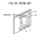
- these probe-type semiconductor strain sensors comprise: a cantilever arm portion (beam portion) 1 having a free end 1a, formed by selectively etching a part of a semiconductor substrate 2 so as to be U-shaped; and a gage portion 3 formed near the fixed end (root) of the cantilever arm portion 1.
- the gage portion 3 detects stress/strain appearing at this portion in response to deflection of the free end 1a, so as to produce an output by converting the strain to an electric signal.
- the gage portion is constructed with a piezo element.
- a resistance bridge circuit such as a Wheatstone bridge or the like.
- US 5279162 discloses a semiconductor sensor comprising a semiconductor cantilever probe with a three terminal field effect transistor used for a Schottky junction.
- WO 97/24915 discloses a microelectronics deformation sensor comprising a single crystal semiconductor base and cantilever probe. A Schottky junction is formed on the base adjacent the supported end of the cantilever.
- An object of the present invention is to provide a semiconductor strain sensor which mitigates the above-mentioned problems and which outputs deflection of the probe with high response speed and with a large signal change. It is an object of the invention to provide a method of manufacturing the sensor. It is also an object of the invention to provide a scanning probe microscope adopting the semiconductor strain sensor for the probe.
- the present invention may be characterised by the following means:
- a cantilever-type semiconductor stress/strain sensor can be produced easily.
- the electric characteristic (diode characteristic) of the Schottky junction changes rapidly.
- the strain is measured with high accuracy as the angle between the surface of the sample and the exploring needle is about 90 degrees.
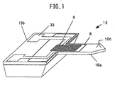
- FIG. 1 is a perspective view showing a general construction of a semiconductor probe according to the present invention.
- a probe 10 comprises an arm portion 10a having a free end, an exploring needle 10c being the tip of the arm portion, a supporting portion 10b holding and fixing the arm portion, a sensor portion 9, and thin film 8 (insulation film 40) formed in the region including at least the sensor portion 9.
- a Schottky junction is used for the sensor portion.
- An electrode for the detecting signal is connected to the sensor portion with wiring 33.
- Low resistance materials such as mainly Al, W, Ti, Ta, Cr, and so on are used for the wiring material. Among these materials, Al is the most generally applicable.
- the thin film 8 functions to pre-stress the sensor portion 9.
- the use of compressive stress is desirable because the direction of the exploring needle 10c is almost perpendicular with respect to the sample and this enables accurate sample observation as the arm portion 10a bends to the under side shown in Fig. 1.
- Layer insulation film 30 can replace the insulation film 40 at the location where stress is applied.
- the thin film 8 can be omitted.
- Stress can be applied to the sensor portion by using a pre-stress material for the wiring 33 so as to replace the thin film 8. Namely, any material except an insulation film can be used if the thin film 8 applies stress to the sensor portion 9 and does not exert a bad influence such as short-circuiting the electric characteristic of the sensor portion 9.
- the shape of the sample can be observed at the tip part of the arm portion 10a without the exploring needle 10c, it is desirable that the exploring needle 10c is formed in order to obtain high accuracy and high resolution. In order to obtain high accuracy and high resolution, it is desirable that the exploring needle 10c is longer than the height of the raggedness of the observed sample and that the diameter of the tip is small.
- Various shapes can be used, such as the substantial rectangular shape shown in Fig. 1, or a U-shape, or the like, so as to allow design in response to the characteristic use of the arm portion 10a.
- Fig. 2A is a plan view of a probe-type semiconductor strain sensor of a first embodiment of the present invention, particularly for describing the arm portion 10b and the sensor portion 9 of Fig. 1.
- Fig. 2B is a cross sectional view taken along line A-A' of Fig. 2A.
- Fig. 2C is a cross sectional view taken along line B-B' of Fig. 2A.
- the insulation 40 (thin film 8) is not shown.
- the probe 10 of this embodiment comprises a U-shaped cantilever arm portion 10a and a supporting portion 10b. At the tip of the cantilever arm portion 10a, an exploring needle 10c for SPM is formed.
- the probe 10 comprises an N-type substrate 31, and on a surface thereof an electrode 32 is Schottky-joined in a U shape along the inside of the arm portion 10a. The electrode 32 is not formed where the layer insulation film 30 is formed.
- an N + contact domain 21 is formed in the surface of the N-type substrate 31 and electrodes 22 are connected thereto. Electrodes 22 are connected to the wiring 33 shown in Fig. 1 and supply bias voltage (current). They carry the detection signal. It is possible to produce the electrodes 22 with the same material as the wiring 33, and both can be formed at the same time.
- An insulation film 40 such as, for example, a SiO 2 film, a Si 3 N 4 film, or the like is provided over the surface of the N-type substrate 31 and can constitute the thin film 8 for pre-stressing the Schottky junction 50. It is desirable to form the insulation film 40 so that the pre-stress/strain is about 1x10 9 Pa. However, the value is determined depending on the structure of the junction portion and the manufacturing procedure.
- the insulation film 40 it is not necessary for the insulation film 40 to be formed over all of the surface of the N-type substrate 31.
- the film may be formed, for example, only over the surface of the cantilever arm portion 10a or only over the part between the arm portion 10a and the supporting portion 10b. The requirement is to pre-stress the Schottky junction 50 between the substrate 31 and the electrode 32.
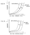
- Figs. 3A and 3B are views showing an example of a diode characteristic of a Schottky junction subjected to stress/strain.
- Fig. 3A shows the forward bias characteristic
- Fig. 3B shows the reverse bias characteristic. It is noted that forward direction current to forward bias changes when stress/strain appears at the Schottky junction 50 during forward bias. During reverse bias too, break voltage changes and leakage current changes too when stress/strain appears.
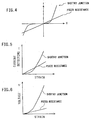
- Figs. 4 to 6 are respective views of the current-voltage (I-V) characteristic of the Schottky junction, current (I) strain characteristic, and voltage (V) strain characteristic compared with a piezo element (referred to as a piezo resistance in the drawings).
- the rate of change of current I and voltage V to stress are larger in the Schottky junction than in the piezo element at larger stress values, as shown in Figs. 5 and 6. Therefore, by forming the Schottky junction 50 at the beam portion of the probe 10 and by detecting the change of the diode characteristic in the region of the larger rate of change as in the present embodiment, detection sensitivity improves so as to correctly measure deflection of the probe 10 without using a difficult to control bridge circuit such as Wheatstone bride and the like.
- the rate of change of the diode characteristic as a result of deflection of the probe is larger for larger deflections, and sufficient detecting sensitivity cannot be obtained when the deflection is small and a small detection region is used.
- signal processing With a small region for detecting stress/strain, signal processing becomes rather complex because the current I changes as a secondary function of stress/strain, as shown in Fig. 5.
- the Schottky junction 50 is pre-stressed by the insulation film 40 (the thin film 8). Therefore, strain appearing transiently depending on displacement during observation and the pre-stress are superimposed. Because of that, larger strain appears compared with the case that the insulation film 40 is not formed. In the large stress/strain region, signal processing at actual observation values becomes easy as the current I changes substantially linearly to stress/strain. The above-mentioned change depends on the structure of the Schottky junction and the manufacturing process. Therefore, changing the quantity of the characteristic is not fixed and can show a similar characteristic as a piezo element depending on conditions.
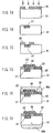
- Figs. 7A to 7F are sectional views of process steps showing a method of manufacturing said probe-type semiconductor strain sensor with the structure described in Fig. 2A.
- Figs. 7A to 7F show a sectional structure taken along the line B-B' of Fig. 2A.
- an N-type semiconductor substrate 31 is etched to the probe shape of Fig. 2, and a resist 81 is applied over the whole of one surface.
- a mask is formed by selectively removing only part of the resist equivalent to the N + contact domain 21. This is achieved using the well-known photo resist technique (Fig. 7A).
- an N-type impurity for example,-phosphorus
- Fig. 7B an N-type impurity
- an SiO 2 insulation film 30 is formed on the surface of the substrate.
- the part equivalent to the N + contact domain 21 and the part equivalent to the Schottky junction 50 are opened so as to expose the N + contact domain 21 and the Schottky junction domain (Fig. 7C).
- the Schottky junction 50 is formed by ohmic contact of an electrode 22 to the N + contact domain 21 and by Schottky-joining an electrode 32 to the Schottky junction domain (Fig. 7D).
- an insulation film 40a is formed to pre-stress the Schottky junction 50 (Fig. 7E). Although the insulation film 40 (40a) is formed as shown in the present embodiment, the insulation film 40 (40b) may be formed on the back of the substrate (Fig. 7F).
- Fig. 8A is a plan view of a semiconductor probe of a second embodiment according to the present invention.
- Fig. 8B is a cross sectional view taken along the line C-C' of Fig. 8A. The same symbols are used as previously to show the same or similar components.
- the present embodiment is characterised in that Schottky junction 50 is actually formed over the whole surface of the arm portion 10a.
- the area of the Schottky junction is comparatively small as the Schottky junction 50 is formed only over a part of the surface of the arm portion 10a. Because of that, while leakage current is small, it is difficult to obtain high sensitivity.
- the second embodiment is characterised in that high sensitivity is obtained even though the leakage current increases a little compared with said first embodiment; as a result of the Schottky junction 50 being formed over the whole surface of the arm portion 10a.
- Said insulation film 40 (thin film 8) for pre-stressing the Shottky junction 50 may be formed on at least one of the front or back surface in any of these embodiments.
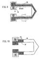
- Fig. 9 is a plan view of a third embodiment of the present invention.
- the same symbols are used as previously to show the same or similar components.
- the embodiment is characterised in that an electrode 32, namely a Schottky junction 50, is formed in a band shape at the center portion of the arm portion 10 so that the Schottky junction is not exposed at end surfaces of the arm portion 10a.
- leakage current generally appears near the end surface of the PN junction, high sensitivity is obtained while leakage current is reduced even though the manufacturing process becomes a little complex.
- Fig. 10 is a plan view of a fourth embodiment of the present invention.
- the same symbols are used as previously to show the same or similar components.
- the present embodiment is based on the fact that strain caused by displacement of the probe 10 is concentrated on the junction between the arm portion 10a and the supporting portion 10b, namely a beam portion of the probe 10, and at all other points the strain is less.
- the present embodiment is characterised in that an electrode 32 (a Schottky junction 50) is formed only at said beam portion. According to the present embodiment, high sensitivity is obtained while leakage current is reduced; since the shottky junction is not formed at any part not contributing to the detection of strain.
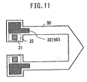
- Fig. 11 is a plan view of a fifth embodiment of the present invention.
- the same symbols are used as previously to show the same or similar components.
- the present embodiment is characterised in that an electrode 32 (a Schottky junction 50) is formed only at the beam portion of the probe 10, and is there formed in a band shape at the center portion of the probe 10; in order to decrease leakage current, similarly to said fourth embodiment.
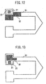
- Figs. 12 and 13 are plan views of a sixth and a seventh embodiment of the present invention, respectively. The same symbols are used as previously to show the same or similar components.
- Each of these embodiments is characterised in that the electrode 32 (the Schottky junction 50) is similar to that of said fourth and fifth embodiments respectively, but is formed only on one of said beam portions. According to the sixth and seventh embodiments, leakage current is sharply decreased, although detection sensitivity decreases a little.
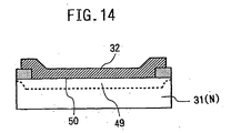
- a metal electrode is connected to the N-type substrate 31 to obtain the Schottky junction in each of the above mentioned embodiments, alternatively a metal electrode may be contacted to a P-type substrate to obtain the Schottky junction.
- leakage current resulting from a spread of the surface charge layer 49, as shown in Fig. 14, increases as a result of reverse bias being applied to the Schottky junction 50.
- leakage current appears at the end portions of the arm portion 10a. Because of that, a new problem may appear in that the measuring sensitivity may decrease. Therefore, in each embodiment of the present invention described below, such an increase of leakage current is suppressed.
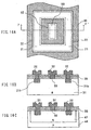
- Fig. 15A is a plan view of an eighth embodiment of the present invention.
- Figs. 15B and 15C are different possible sectional views taken along line E-E' of Fig. 15A. These figures show to enlarged scale the beam bending portion at the base or root of the arm portion 10a.
- an electrode 32 is formed in a band shape at the center of the beam portion of the probe 10 so that the Schottky junction 50 is not exposed at the end surfaces of the probe 10, as shown in Fig. 15A.
- An N + contact domain 21a is formed in a surface of an N-type substrate 31 between the end portion 10a and the Schottky junction 50, which serves to prevent enlargement of the space charge layer.
- N-type semiconductor domain 47 By forming an N-type semiconductor domain 47 in the main surface of a P-type substrate 48 in an island-shape and by forming the above-mentioned configuration in the N-type semiconductor domain 47, leakage current is further suppressed by separation with a PN junction.
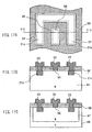
- Fig. 16A is a plan view of a ninth embodiment of the present invention.
- Figs. 16B and 16C are different possible sectional views taken along line F-F' of Fig. 16A. The same symbols are used as previously to show the same or similar components.
- the present embodiment is characterised in that an electrode 32 is formed in a band shape at the center portion of a probe 10 so that the Schottky junction 50 is not exposed at the end surfaces of the probe 10 and an N + contact domain 21b is formed to surround the Schottky junction 50 as shown in Fig. 16A.
- the horizontal spread of the space charge layer 49 is prevented by the N + contact domain 21 so that it does not reach the end portion of the arm portion 10a. Therefore, the measuring sensitivity is kept high because an increase in leakage current is suppressed.
- leakage current is further suppressed by separation with a PN junction.
- Fig. 17A is a plan view of a ninth embodiment of the present invention.
- Figs. 17B and 17C are different possible sectional views taken along line G-G' of Fig. 17A. The same symbols are used as previously to show the same or similar components.
- the present embodiment is characterised in that an electrode 32 is formed at the center portion of a probe 10 so that the Schottky junction 50 is not exposed at the end surfaces of the probe 10 and an N + contact domain 21c is formed to surround the Schottky junction 50 in three directions.
- leakage current appearing at the circumference of the Schottky junction 50 is suppressed by the N + contact domain 21c and the leakage current does not reach the end portions of the probe 10. Therefore, measuring sensitivity is kept high because any increase of leakage current is suppressed.
- leakage current is further suppressed by separation with a PN junction.
- Figs. 18A and 18B show an example in which the sensor of the ninth embodiment of the present invention (Fig. 16) is actually formed on a rectangular arm portion.
- Fig. 18A is a plan view of the embodiment.
- Fig. 18B is a sectional view taken along the line H-H' of Fig. 18A. The same symbols are used as previously to show the same or similar components.
- the width of the sensor becomes wide as the Schottky junction 50 is formed at the center of the sensor portion, and at a circumference portion an N + contact domain 21 is formed. Therefore, in order to make the width of the arm portion 10a small, a rectangular arm is easier than a U-shape arm for the design of the arm portion.
- the thin film for providing the pre-stress is the insulation film 40 in each embodiment, the present invention is not limited thereby.
- the thin film may be a conductive film or a semiconductive film so long as the insulation film is previously formed on the surface of the substrate without providing a pre-stress and the thin film is formed on the insulation film.
- Fig. 19 is a block diagram showing a configuration of a scanning probe microscope using the present invention.
- a sample 52 is set on a three dimensions sample stage 55, and an exploring needle 31 b of the probe 10, configured as described above, is arranged facing the stage.
- the diode characteristic of the Schottky junction formed in the probe 10 is detected at a measuring portion 71 and input to a non-inversion input terminal (+) of a differential amplifier 75 as a bending signal S1.
- a reference value relative to bending of the probe 10 is input to an inversion input terminal (-) of the differential amplifier 75 so that the output of the differential amplifier 75 becomes zero when bending is zero, for example.
- An error signal S2 output from the differential amplifier is input to a control portion 76.
- the control portion 76 controls an actuator driving amplifier 70 so that the error signal S2 approaches zero.
- the output signal of the control portion 76 is also supplied to a CRT as a luminance signal.
- a scanning signal generating portion 78 supplies a differential signal, for slightly moving the sample 52 in XYZ directions, to the actuator driving amplifier 70.
- the scanning signal generating portion 78 also supplies a raster scanning signal to the CRT.
- the present invention has the following advantages:
Landscapes
- Physics & Mathematics (AREA)
- Health & Medical Sciences (AREA)
- General Health & Medical Sciences (AREA)
- General Physics & Mathematics (AREA)
- Nuclear Medicine, Radiotherapy & Molecular Imaging (AREA)
- Radiology & Medical Imaging (AREA)
- Chemical & Material Sciences (AREA)
- Engineering & Computer Science (AREA)
- Nanotechnology (AREA)
- Analytical Chemistry (AREA)
- Crystallography & Structural Chemistry (AREA)
- Measurement Of Length, Angles, Or The Like Using Electric Or Magnetic Means (AREA)
- Length Measuring Devices With Unspecified Measuring Means (AREA)
- Pressure Sensors (AREA)
Claims (11)
- Halbleiterverformungssensor umfassend:eine Halbleiterauslegersonde (10) mit einem Ursprung, welcher in einem Abstand von einem freien Ende desselben angebracht ist;
undeinen Schottky-Übergang (9), welcher an dem Ursprung der Halbleitersonde vorgesehen ist, dadurch gekennzeichnet, dass er
umfasst:einen Hochkonzentrationskontaktbereich (21 ), welcher in einer Oberfläche der Halbleitersonde und getrennt von dem Schottky-Übergang ausgebildet ist; undeine Elektrode (22), welche mit dem Hochkonzentrationskontaktbereich verbunden ist. - Halbleiterverformungssensor nach Anspruch 1, wobei die Elektrode mit dem Hochkonzentrationskontaktbereich ohmsch kontaktiert ist.
- Halbleiterverformungssensor nach Anspruch 1 oder Anspruch 2, wobei der Schottky-Übergang eine Bandform entlang des Endabschnitts der Sonde aufweist.
- Halbleiterverformungssensor nach Anspruch 1 oder Anspruch 2, wobei der Schottky-Übergang im Wesentlichen über der gesamte Oberfläche der Sonde vorgesehen ist.
- Halbleiterverformungssensor nach Anspruch 1 oder Anspruch 2, wobei der Schottky-Übergang in einem Bereich, der von den Endabschnitten der Sonde einen Abstand aufweist, bereitgestellt ist.
- Halbleiterverformungssensor nach Anspruch 5, wobei der Hochkonzentrationskontaktbereich zwischen dem Schottky-Übergang und den Endabschnitten des Substrats ausgebildet ist.
- Halbleiterverformungssensor nach Anspruch 5, wobei der Hochkonzentrationskontaktbereich den Schottky-Übergang in einer Oberfläche des Substrats umgibt.
- Halbleiterverformungssensor nach einem der Ansprüche 5 und 7, wobei die Halbleitersonde so konstruiert ist, dass ein Halbleiterbereich vom leitfähigen Typ verschieden von dem Halbleitersubstrat in dem Halbleitersubstrat ausgebildet ist und eine Elektrode an der Oberfläche des Halbleiterbereichs Schottky-verbunden ist, um den Schottky-Übergang auszubilden.
- Verfahren zum Herstellen eines Halbleiterverformungssensors umfassend die Schritte:Ausbilden einer Halbleitersonde (10) durch Ätzen eines Halbleitersubstrats, um eine Sondenform zu bilden;wahlweises Ausbilden eines Hochkonzentrationsbereichs (21) in der Oberfläche der Halbleitersonde;wahlweises Schottky-Verbinden einer ersten Elektrode (22) mit dem Ursprungsabschnitt (9) der Halbleitersonde an einer von dem Hochkonzentrationskontaktbereich getrennten Position; undVerbinden einer zweiten Elektrode (32) mit dem Hochkonzentrationskontaktbereich.
- Verfahren zum Herstellen eines Halbleiterverformungssensors nach Anspruch 9, ferner umfassen einen Schritt zum Ausbilden eines dünnen Films (8) auf wenigstens einer Oberfläche der Probe, um den Schottky-Übergang einer Druckbelastung auszusetzen.
- Mikroskop mit abtastender Sonde, welches den Halbleiterverformungssensor gemäß einem der Ansprüche 1 bis 8 verwendet.
Applications Claiming Priority (6)
| Application Number | Priority Date | Filing Date | Title |
|---|---|---|---|
| JP28411697 | 1997-10-16 | ||
| JP28411697 | 1997-10-16 | ||
| JP284116/97 | 1997-10-16 | ||
| JP28091098 | 1998-10-02 | ||
| JP280910/98 | 1998-10-02 | ||
| JP28091098A JP3700910B2 (ja) | 1997-10-16 | 1998-10-02 | 半導体歪センサ及びその製造方法ならびに走査プローブ顕微鏡 |
Publications (2)
| Publication Number | Publication Date |
|---|---|
| EP0909937A1 EP0909937A1 (de) | 1999-04-21 |
| EP0909937B1 true EP0909937B1 (de) | 2003-12-10 |
Family
ID=26553978
Family Applications (1)
| Application Number | Title | Priority Date | Filing Date |
|---|---|---|---|
| EP98308447A Expired - Lifetime EP0909937B1 (de) | 1997-10-16 | 1998-10-15 | Halbleiter-Dehnungs-Sensor, Verfahren zu dessen Herstellung und Rastersondenmikroskop |
Country Status (4)
| Country | Link |
|---|---|
| US (1) | US6211540B1 (de) |
| EP (1) | EP0909937B1 (de) |
| JP (1) | JP3700910B2 (de) |
| DE (1) | DE69820380T2 (de) |
Families Citing this family (12)
| Publication number | Priority date | Publication date | Assignee | Title |
|---|---|---|---|---|
| US6632691B1 (en) * | 2002-04-11 | 2003-10-14 | Solid State Measurements, Inc. | Apparatus and method for determining doping concentration of a semiconductor wafer |
| US7763947B2 (en) * | 2002-04-23 | 2010-07-27 | Sharp Laboratories Of America, Inc. | Piezo-diode cantilever MEMS |
| US6647809B1 (en) | 2002-08-29 | 2003-11-18 | The United States Of America As Represented By The Administrator Of The National Aeronautics And Space Administration | Silicon carbide high temperature anemometer and method for assembling the same |
| US7009268B2 (en) * | 2004-04-21 | 2006-03-07 | Hewlett-Packard Development Company, L.P. | Wheatstone bridge scheme for sensor |
| KR100579377B1 (ko) * | 2004-10-28 | 2006-05-12 | 삼성에스디아이 주식회사 | 이차 전지 |
| DE102005038245B4 (de) * | 2005-08-12 | 2010-09-16 | Fraunhofer-Gesellschaft zur Förderung der angewandten Forschung e.V. | Vorrichtung zur Schwingungsanregung eines einseitig in einem Rasterkraftmikroskop befestigten Federbalkens |
| DE102006011660A1 (de) * | 2006-03-12 | 2007-09-13 | Fraunhofer-Gesellschaft zur Förderung der angewandten Forschung e.V. | Verfahren zur Ermittlung einer Dotierungsdichte in einer Halbleiterprobe |
| JP2008151673A (ja) * | 2006-12-19 | 2008-07-03 | Japan Advanced Institute Of Science & Technology Hokuriku | 走査型プローブ顕微鏡用化合物半導体カンチレバー、及びその製造法 |
| WO2011148774A1 (ja) * | 2010-05-24 | 2011-12-01 | 独立行政法人物質・材料研究機構 | 表面応力センサ |
| DE102010030345B4 (de) * | 2010-06-22 | 2019-05-09 | Robert Bosch Gmbh | Verfahren zur Herstellung einer piezoresistiven Sensoranordnung und Sensoranordnung |
| CN102079499B (zh) * | 2010-12-20 | 2012-05-30 | 北京大学 | 一种悬臂梁微量检测传感器及其制备方法 |
| CN114136214B (zh) * | 2021-12-02 | 2024-03-26 | 中国人民解放军军事科学院国防科技创新研究院 | 一种基于双刚度方波状结构的位移传感器 |
Family Cites Families (10)
| Publication number | Priority date | Publication date | Assignee | Title |
|---|---|---|---|---|
| EP0363005B1 (de) * | 1988-09-02 | 1996-06-05 | Honda Giken Kogyo Kabushiki Kaisha | Halbleitermessaufnehmer |
| JPH05196458A (ja) * | 1991-01-04 | 1993-08-06 | Univ Leland Stanford Jr | 原子力顕微鏡用ピエゾ抵抗性片持ばり構造体 |
| US5444244A (en) * | 1993-06-03 | 1995-08-22 | Park Scientific Instruments Corporation | Piezoresistive cantilever with integral tip for scanning probe microscope |
| EP0695927A3 (de) * | 1994-08-01 | 1996-06-26 | Motorola Inc | Detektor-Umformer unter Verwendung eines Schottky-Übergangs mit einer erhöhten Ausgangsspannung |
| US5632841A (en) * | 1995-04-04 | 1997-05-27 | The United States Of America As Represented By The Administrator Of The National Aeronautics And Space Administration | Thin layer composite unimorph ferroelectric driver and sensor |
| US5838005A (en) * | 1995-05-11 | 1998-11-17 | The Regents Of The University Of California | Use of focused ion and electron beams for fabricating a sensor on a probe tip used for scanning multiprobe microscopy and the like |
| US5713667A (en) * | 1995-06-07 | 1998-02-03 | Advanced Micro Devices, Inc. | Temperature sensing probe for microthermometry |
| WO1997009584A1 (en) * | 1995-09-01 | 1997-03-13 | International Business Machines Corporation | Cantilever with integrated deflection sensor |
| IL116536A0 (en) * | 1995-12-24 | 1996-03-31 | Harunian Dan | Direct integration of sensing mechanisms with single crystal based micro-electric-mechanics systems |
| EP0802394B1 (de) * | 1996-04-18 | 2003-06-11 | Seiko Instruments Inc. | Halbleiterdehnungssensoren mit pn Übergang, Rastersondenmikroskop |
-
1998
- 1998-10-02 JP JP28091098A patent/JP3700910B2/ja not_active Expired - Fee Related
- 1998-10-15 DE DE69820380T patent/DE69820380T2/de not_active Expired - Lifetime
- 1998-10-15 EP EP98308447A patent/EP0909937B1/de not_active Expired - Lifetime
- 1998-10-15 US US09/173,035 patent/US6211540B1/en not_active Expired - Lifetime
Also Published As
| Publication number | Publication date |
|---|---|
| JPH11183487A (ja) | 1999-07-09 |
| US6211540B1 (en) | 2001-04-03 |
| JP3700910B2 (ja) | 2005-09-28 |
| DE69820380T2 (de) | 2004-05-27 |
| DE69820380D1 (de) | 2004-01-22 |
| EP0909937A1 (de) | 1999-04-21 |
Similar Documents
| Publication | Publication Date | Title |
|---|---|---|
| EP0584233B1 (de) | Submikron Spitzenanordnung mit gegenüberliegenden Spitzen | |
| EP0909937B1 (de) | Halbleiter-Dehnungs-Sensor, Verfahren zu dessen Herstellung und Rastersondenmikroskop | |
| US5386720A (en) | Integrated AFM sensor | |
| KR100214152B1 (ko) | 원자력 현미경용 압저항 캔틸레버 | |
| US5338932A (en) | Method and apparatus for measuring the topography of a semiconductor device | |
| US6851301B2 (en) | Cantilever for scanning probe microscope | |
| US7520165B2 (en) | Micro structure, cantilever, scanning probe microscope and a method of measuring deformation quantity for the fine structure | |
| JPH11515092A (ja) | 高感度力検出のための超小型化ねじれキャンティレバー | |
| US6383823B1 (en) | Probe for scanning probe microscope (SPM) and SPM device | |
| US6388252B1 (en) | Self-detecting type of SPM probe and SPM device | |
| EP0802394B1 (de) | Halbleiterdehnungssensoren mit pn Übergang, Rastersondenmikroskop | |
| US20020178801A1 (en) | Self-detecting type SPM probe | |
| JPH09304409A (ja) | 力変位センサ付カンチレバー | |
| EP0905475B1 (de) | Halbleiter-Dehnungs-Sensor, Vefahren zu dessen Herstellung und Rastersondenmikroskop | |
| JP2001108605A (ja) | 走査型プローブ顕微鏡用カンチレバー及びその製造方法、並びに走査型プローブ顕微鏡及び表面電荷測定顕微鏡 | |
| JP3433782B2 (ja) | 走査プローブ顕微鏡およびその半導体歪センサならびにその製造方法 | |
| JP3124485B2 (ja) | 半導体歪センサおよび走査型原子間力顕微鏡用カンチレバー | |
| JP3768639B2 (ja) | カンチレバー型プローブ及び該プローブを備えた走査型プローブ顕微鏡 | |
| JPH10282129A (ja) | 半導体歪センサおよびこれを用いた走査型プローブ顕微鏡 | |
| JP3188022B2 (ja) | 集積型afmセンサー駆動回路 | |
| JPH05312562A (ja) | 集積型afmセンサー | |
| JP2000111563A (ja) | 自己検知型spmプロ―ブ | |
| JPH07325092A (ja) | 集積型spmセンサーおよびその温度測定回路 | |
| JP2004055592A (ja) | 半導体力検出装置 | |
| JPH07146301A (ja) | 集積型spmセンサー |
Legal Events
| Date | Code | Title | Description |
|---|---|---|---|
| PUAI | Public reference made under article 153(3) epc to a published international application that has entered the european phase |
Free format text: ORIGINAL CODE: 0009012 |
|
| AK | Designated contracting states |
Kind code of ref document: A1 Designated state(s): CH DE FR GB IT LI NL |
|
| AX | Request for extension of the european patent |
Free format text: AL;LT;LV;MK;RO;SI |
|
| 17P | Request for examination filed |
Effective date: 19991020 |
|
| RIN1 | Information on inventor provided before grant (corrected) |
Inventor name: ICHIHARA, SUSUMU Inventor name: SHIRAKAWABE, YOSHIHARU Inventor name: SHIMIZU, NOBUHIRO Inventor name: TAKAHASHI, HIROSHI Inventor name: DESPONT, MICHEL |
|
| AKX | Designation fees paid |
Free format text: CH DE FR GB IT LI NL |
|
| RAP1 | Party data changed (applicant data changed or rights of an application transferred) |
Owner name: IBM CORPORATION |
|
| 17Q | First examination report despatched |
Effective date: 20020923 |
|
| RAP1 | Party data changed (applicant data changed or rights of an application transferred) |
Owner name: IBM CORPORATION Owner name: SEIKO INSTRUMENTS INC. |
|
| GRAH | Despatch of communication of intention to grant a patent |
Free format text: ORIGINAL CODE: EPIDOS IGRA |
|
| GRAS | Grant fee paid |
Free format text: ORIGINAL CODE: EPIDOSNIGR3 |
|
| GRAA | (expected) grant |
Free format text: ORIGINAL CODE: 0009210 |
|
| AK | Designated contracting states |
Kind code of ref document: B1 Designated state(s): CH DE FR GB IT LI NL |
|
| PG25 | Lapsed in a contracting state [announced via postgrant information from national office to epo] |
Ref country code: NL Free format text: LAPSE BECAUSE OF FAILURE TO SUBMIT A TRANSLATION OF THE DESCRIPTION OR TO PAY THE FEE WITHIN THE PRESCRIBED TIME-LIMIT Effective date: 20031210 Ref country code: IT Free format text: LAPSE BECAUSE OF FAILURE TO SUBMIT A TRANSLATION OF THE DESCRIPTION OR TO PAY THE FEE WITHIN THE PRESCRIBED TIME-LIMIT;WARNING: LAPSES OF ITALIAN PATENTS WITH EFFECTIVE DATE BEFORE 2007 MAY HAVE OCCURRED AT ANY TIME BEFORE 2007. THE CORRECT EFFECTIVE DATE MAY BE DIFFERENT FROM THE ONE RECORDED. Effective date: 20031210 Ref country code: FR Free format text: LAPSE BECAUSE OF FAILURE TO SUBMIT A TRANSLATION OF THE DESCRIPTION OR TO PAY THE FEE WITHIN THE PRESCRIBED TIME-LIMIT Effective date: 20031210 |
|
| REG | Reference to a national code |
Ref country code: GB Ref legal event code: FG4D |
|
| REG | Reference to a national code |
Ref country code: CH Ref legal event code: EP |
|
| REF | Corresponds to: |
Ref document number: 69820380 Country of ref document: DE Date of ref document: 20040122 Kind code of ref document: P |
|
| REG | Reference to a national code |
Ref country code: CH Ref legal event code: NV Representative=s name: PATENTANWAELTE SCHAAD, BALASS, MENZL & PARTNER AG |
|
| NLV1 | Nl: lapsed or annulled due to failure to fulfill the requirements of art. 29p and 29m of the patents act | ||
| PG25 | Lapsed in a contracting state [announced via postgrant information from national office to epo] |
Ref country code: GB Free format text: LAPSE BECAUSE OF NON-PAYMENT OF DUE FEES Effective date: 20041015 |
|
| PLBE | No opposition filed within time limit |
Free format text: ORIGINAL CODE: 0009261 |
|
| STAA | Information on the status of an ep patent application or granted ep patent |
Free format text: STATUS: NO OPPOSITION FILED WITHIN TIME LIMIT |
|
| 26N | No opposition filed |
Effective date: 20040913 |
|
| EN | Fr: translation not filed | ||
| GBPC | Gb: european patent ceased through non-payment of renewal fee |
Effective date: 20041015 |
|
| REG | Reference to a national code |
Ref country code: CH Ref legal event code: PUE Owner name: SII NANO TECHNOLOGY INC. Free format text: SEIKO INSTRUMENTS INC.#8 NAKASE 1-CHOME, MIHAMA-KU#CHIBA-SHI, CHIBA-KEN 261-0023 (JP) $ IBM CORPORATION#NEW ORCHARD ROAD#ARMONK, NY 10504 (US) -TRANSFER TO- SII NANO TECHNOLOGY INC.#8, NAKASE 1-CHOME MIHAMA-KU#CHIBA-SHI, CHIBA (JP) |
|
| REG | Reference to a national code |
Ref country code: CH Ref legal event code: PK |
|
| RAP2 | Party data changed (patent owner data changed or rights of a patent transferred) |
Owner name: INTERNATIONAL BUSINESS MACHINES CORPORATION Owner name: SEIKO INSTRUMENTS INC. |
|
| PGFP | Annual fee paid to national office [announced via postgrant information from national office to epo] |
Ref country code: DE Payment date: 20101013 Year of fee payment: 13 Ref country code: CH Payment date: 20101012 Year of fee payment: 13 |
|
| REG | Reference to a national code |
Ref country code: CH Ref legal event code: PL |
|
| PG25 | Lapsed in a contracting state [announced via postgrant information from national office to epo] |
Ref country code: CH Free format text: LAPSE BECAUSE OF NON-PAYMENT OF DUE FEES Effective date: 20111031 Ref country code: LI Free format text: LAPSE BECAUSE OF NON-PAYMENT OF DUE FEES Effective date: 20111031 Ref country code: DE Free format text: LAPSE BECAUSE OF NON-PAYMENT OF DUE FEES Effective date: 20120501 |
|
| REG | Reference to a national code |
Ref country code: DE Ref legal event code: R119 Ref document number: 69820380 Country of ref document: DE Effective date: 20120501 |