EP0903859B1 - Frequenzteiler mit geringem Stromverbrauch - Google Patents
Frequenzteiler mit geringem Stromverbrauch Download PDFInfo
- Publication number
- EP0903859B1 EP0903859B1 EP98116970A EP98116970A EP0903859B1 EP 0903859 B1 EP0903859 B1 EP 0903859B1 EP 98116970 A EP98116970 A EP 98116970A EP 98116970 A EP98116970 A EP 98116970A EP 0903859 B1 EP0903859 B1 EP 0903859B1
- Authority
- EP
- European Patent Office
- Prior art keywords
- divider
- frequency
- signal
- input
- stage
- Prior art date
- Legal status (The legal status is an assumption and is not a legal conclusion. Google has not performed a legal analysis and makes no representation as to the accuracy of the status listed.)
- Expired - Lifetime
Links
- 230000001419 dependent effect Effects 0.000 claims description 2
- 238000010586 diagram Methods 0.000 description 3
- 230000005611 electricity Effects 0.000 description 2
- 230000009977 dual effect Effects 0.000 description 1
- 238000010079 rubber tapping Methods 0.000 description 1
- 230000001360 synchronised effect Effects 0.000 description 1
Images

Classifications
-
- H—ELECTRICITY
- H03—ELECTRONIC CIRCUITRY
- H03K—PULSE TECHNIQUE
- H03K23/00—Pulse counters comprising counting chains; Frequency dividers comprising counting chains
- H03K23/64—Pulse counters comprising counting chains; Frequency dividers comprising counting chains with a base or radix other than a power of two
- H03K23/66—Pulse counters comprising counting chains; Frequency dividers comprising counting chains with a base or radix other than a power of two with a variable counting base, e.g. by presetting or by adding or suppressing pulses
- H03K23/667—Pulse counters comprising counting chains; Frequency dividers comprising counting chains with a base or radix other than a power of two with a variable counting base, e.g. by presetting or by adding or suppressing pulses by switching the base during a counting cycle
Definitions
- the present invention relates to a frequency divider the preamble of claim 1.
- frequency divider is intended to include so-called “Dual Modulus Prescaler” can be understood as they are in frequency synthesizers of mobile telecommunication systems Find use. Such frequency dividers point between 1 / N and 1 / (N + 1) switchable division factors, where N typically 64 or 128, work with frequencies in the order of 1 GHz and are part of everyone GSM or DECT phones. Because of the usually existing Battery supply for the devices is low power consumption essential.
- An intermediate divider creates from the first Intermediate signal depending on a changeover signal in the case of a desired division factor 1 / N a second intermediate signal with the frequency f / 8 by reducing the frequency with the division factor 1/4 and in the case of a desired division factor 1 / (N + 1) with another second intermediate signal the frequency f / 10 by lowering the frequency with the division factor 1.5.
- a divider extension unit with 2N-2 divider stages delivers an output signal with its penultimate divider stage with the frequency f / N or f / (N + 1), and a logic circuit generated from a control signal and a Output signal of the divider extension unit, the changeover signal.
- the object underlying the invention is one Specify frequency divider of the type specified at the outset, which has a particularly low power consumption. This The object is achieved on the basis of the features of patent claim 1.
- the further claim 2 relates to an advantageous Embodiment of the invention.
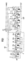
- a frequency divider for the division factors 1/64 and 1/65 is shown by way of example in FIG. 1, this having an input-side frequency halve H, an intermediate divider 4/5 and a divider extension EXT.
- the input-side frequency bisector H generates from an input signal IN with the frequency f an intermediate signal 1 which only has the frequency f / 2.
- a second intermediate signal 2 with the frequency f / 8 is obtained from the first intermediate signal by reducing the frequency with the division factor 1/4 and in the case of a desired division factor 1 / (N + 1) generates the intermediate signal 2 with the frequency f / 10 from the first intermediate signal by reducing the frequency with the division factor 1/5.
- the divider extension EXT has 2 N-2 divider stages (FF5 ... FF8), the penultimate divider stage FF7 of which provides an output signal OUT with the frequency f / N or f / (N + 1).
- the switchover signal U is formed by an AND gate A3 from a negated control signal MOD and from the negated output signals 3 ... 6 of the divider stages FF5 ... FF8.
- the frequency bisector is designed here such that the input signal IN of the frequency divider serves as a clock signal for a D flip-flop FF1, the inverted input of which carries signal 1 and is fed back to the D input.
- the intermediate divider 4/5 contains three flip-flops FF2 ...
- flip-flop FF4 synchronously clocked by the signal 1, the D input of the flip-flop FF2 being connected to an AND gate A1 which combines the switchover signal U with the second signal 2, the D input of flip-flop FF3 is connected to an AND gate A2, which links a negated output signal of flip-flop FF2 with a negated output signal of flip-flop FF4, and the non-inverted output of flip-flop FF3 is connected to the D input of flip-flop FF4 ,
- the flip-flops FF5 ... FF8 of the divider extension EXT are connected here as an asynchronous counter, the clock input of the D-flip-flops FF6 ...
- All flip-flops FF1 ... FF8 are D-type flip-flops with a clock input triggering on positive signal edges.
- the frequency halving on the input side results in a division by 128 or 130 at the output of the last stage of the extension divider EXT.
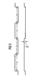
- the output signal OUT is that shown in Figure 1 Circuit shown, the output signal such is that after 34 periods of high level, 32 periods with low level, then again 32 periods high level and finally 32 periods of low level occur again.
- This signal shows next to the desired fundamental wave another signal of half the output frequency and the Amplitude 2/65. This corresponds to an undesired overlay an interference voltage (jitter) with the frequency of the fundamental wave of the output signal.
- FIG. 3 a preferred embodiment of the invention specified, with a modified divider extension EXT 'with a jitter compensation device JK a jitter is avoided at the output OUT.
- the circuit of Figure 3 corresponds except for the modified part extension EXT 'instead the divider extension EXT of the circuit of FIG. 1.
- the jitter compensation device JK exists here, for example in that the inverted output signal 4 of the flip-flop FF6 through a resistor R1 to the clock input of the Flip-flop FF7 is connected and the clock input of the flip-flop A signal 7 is fed to FF7 via a further resistor R2 is that by an AND operation (A4) of the inverted Output signal of the flip-flop FF8 and the inverted control signal MOD is formed.
- This causes the Signal 4 a signal with the amplitude - 2/65 with half Frequency of the output signal admixed and thereby the jitter is eliminated.
- the Jitter compensation device JK generally constructed in such a way that after the first half of the divider stages (FF5, FF6) a dependent on the output signal of the last divider stage (FF8) Signal (7) a clock signal for a first stage (FF7) the second half of the divider stages (FF7, FF8) added becomes.
Landscapes
- Stabilization Of Oscillater, Synchronisation, Frequency Synthesizers (AREA)
- Manipulation Of Pulses (AREA)
Description
- Figur 1
- ein Schaltbild eines beispielhaften Frequenzteilens und
- Figur 2
- Zeitdiagramme zur Erläuterung der Funktionsweise der Schaltung nach Figur 1 und
- Figur 3
- ein Schaltbild eines bevorzugten Ausführungsbeispiels.
Claims (2)
- Frequenzteilerdadurch gekennzeichnet, dassmit einem eingangsseitigen Frequenzhalbierer (H), der aus einem Eingangssignal (IN) mit der Frequenz f ein erstes Zwischensignal (1) bildet, das lediglich die Frequenz f/2 aufweist,mit einem Zwischenteiler (4/5), der, abhängig von einem Umschaltsignal (U), im Falle eines gewünschten Teilungsfaktors 1/N ein zweites Zwischensignal (2) mit der Frequenz f/8 aus dem ersten Zwischensignal durch Herabsetzen der Frequenz mit dem Teilungsfaktor 1/4 erzeugt und im Falle eines gewünschten Teilungsfaktors 1/(N+1) das Zwischensignal (2) mit der Frequenz f/10 aus dem ersten Zwischensignal durch Herabsetzen der Frequenz mit dem Teilungsfaktor 1/5 erzeugt,mit einer Teilererweiterung (EXT) mit 2N-2 Teilerstufen (FF5 ... FF8), deren vorletzte Teilerstufe (FF7) ein Ausgangssignal (OUT) mit der Frequenz f/N bzw. f/(N + 1) liefert undmit einer Verknüpfungsschaltung (A3), die aus einem Steuersignal (MOD) und Ausgangssignalen (3 ... 6) der Teilererweiterung das Umschaltsignal (U) erzeugt,die Teilererweiterung (EXT') eine Jitterkompensationseinrichtung (JK) derart aufweist, dass nach der ersten Hälfte der Teilerstufen (FF5, FF6) ein vom Ausgangssignal der letzten Teilerstufe (FF8) abhängiges Signal (7) einem Taktsignal für eine erste Stufe (FF7) der zweiten Hälfte der Teilerstufen (FF7, FF8) aufaddiert wird.
- Frequenzteiler nach Anspruch 1,bei dem die Teilererweiterung (EXT') einen asynchronen Teiler mit vier Stufen (FF5 ... FF8) aufweist undbei dem die Jitterkompensationseinrichtung (JK) derart aufgebaut ist, dass ein Eingang der dritten Stufe (FF7) über einen ersten Widerstand (R1) mit einem Ausgang (4) der zweiten Stufe (FF6) und über einen zweiten Widerstand (R2) mit einem Ausgang (7) eines UND-Gatters (A4) verbunden ist, dessen erster Eingang mit einem Ausgang einer letzten Stufe (FF8) der Teilererweiterung verbunden ist und dessen zweiter Eingang mit dem invertierten Steuersignal (MOD) beschaltet ist.
Applications Claiming Priority (2)
| Application Number | Priority Date | Filing Date | Title |
|---|---|---|---|
| DE19741210 | 1997-09-18 | ||
| DE19741210 | 1997-09-18 |
Publications (3)
| Publication Number | Publication Date |
|---|---|
| EP0903859A2 EP0903859A2 (de) | 1999-03-24 |
| EP0903859A3 EP0903859A3 (de) | 1999-12-15 |
| EP0903859B1 true EP0903859B1 (de) | 2004-11-24 |
Family
ID=7842840
Family Applications (1)
| Application Number | Title | Priority Date | Filing Date |
|---|---|---|---|
| EP98116970A Expired - Lifetime EP0903859B1 (de) | 1997-09-18 | 1998-09-08 | Frequenzteiler mit geringem Stromverbrauch |
Country Status (4)
| Country | Link |
|---|---|
| US (1) | US6067339A (de) |
| EP (1) | EP0903859B1 (de) |
| JP (1) | JP3571228B2 (de) |
| DE (1) | DE59812296D1 (de) |
Families Citing this family (12)
| Publication number | Priority date | Publication date | Assignee | Title |
|---|---|---|---|---|
| FR2769432B1 (fr) * | 1997-10-03 | 2000-01-28 | Thomson Csf | Diviseur de frequence a modulo variable |
| US6873743B2 (en) * | 2001-03-29 | 2005-03-29 | Fotonation Holdings, Llc | Method and apparatus for the automatic real-time detection and correction of red-eye defects in batches of digital images or in handheld appliances |
| US6751348B2 (en) * | 2001-03-29 | 2004-06-15 | Fotonation Holdings, Llc | Automated detection of pornographic images |
| EP1300950A1 (de) * | 2001-10-05 | 2003-04-09 | Asulab S.A. | Dual Modulus Zähler/Teiler mit Phasenauswahl für einen Frequenzsynthesizer |
| US6760398B2 (en) * | 2001-10-05 | 2004-07-06 | Asulab S.A. | Switched phase dual-modulus prescaler circuit having means for reducing power consumption |
| US6696857B1 (en) | 2003-01-07 | 2004-02-24 | Institute Of Microelectronics | High speed CMOS dual modulus prescaler using pull down transistor |
| US7180341B2 (en) | 2003-05-20 | 2007-02-20 | Nippon Telegraph And Telephone Public Corporation | Variable division method and variable divider |
| US6967507B2 (en) * | 2004-01-15 | 2005-11-22 | Agilent Technologies, Inc. | Dual edge count programmable frequency divider |
| GB2437990B (en) * | 2006-01-24 | 2008-06-25 | Toumaz Technology Ltd | Frequency divider circuits |
| US7486145B2 (en) * | 2007-01-10 | 2009-02-03 | International Business Machines Corporation | Circuits and methods for implementing sub-integer-N frequency dividers using phase rotators |
| CN104113325B (zh) * | 2013-04-19 | 2018-09-28 | 南京中兴软件有限责任公司 | 一种多模可编程分频器 |
| US9679194B2 (en) | 2014-07-17 | 2017-06-13 | At&T Intellectual Property I, L.P. | Automated obscurity for pervasive imaging |
Family Cites Families (8)
| Publication number | Priority date | Publication date | Assignee | Title |
|---|---|---|---|---|
| JPS59181831A (ja) * | 1983-03-31 | 1984-10-16 | Toshiba Corp | 可変分周器 |
| DE3503182A1 (de) * | 1985-01-31 | 1986-08-07 | Deutsche Thomson-Brandt Gmbh, 7730 Villingen-Schwenningen | Programmierbarer zaehler |
| JPS63151217A (ja) * | 1986-12-16 | 1988-06-23 | Fujitsu Ltd | 歯抜け分周回路 |
| JPH034618A (ja) * | 1989-05-31 | 1991-01-10 | Nec Eng Ltd | クロック分周回路 |
| JPH0548433A (ja) * | 1991-08-16 | 1993-02-26 | Nippon Telegr & Teleph Corp <Ntt> | 多段分周器 |
| JPH0590953A (ja) * | 1991-09-30 | 1993-04-09 | Fujitsu Ltd | 半導体論理回路 |
| JPH0645913A (ja) * | 1992-07-24 | 1994-02-18 | Nec Corp | クロック分周回路 |
| JPH07221633A (ja) * | 1994-01-28 | 1995-08-18 | Fujitsu Ltd | 2モジュラスプリスケーラ |
-
1998
- 1998-09-08 EP EP98116970A patent/EP0903859B1/de not_active Expired - Lifetime
- 1998-09-08 DE DE59812296T patent/DE59812296D1/de not_active Expired - Fee Related
- 1998-09-15 US US09/153,060 patent/US6067339A/en not_active Expired - Fee Related
- 1998-09-18 JP JP26493698A patent/JP3571228B2/ja not_active Expired - Fee Related
Also Published As
| Publication number | Publication date |
|---|---|
| EP0903859A3 (de) | 1999-12-15 |
| JP3571228B2 (ja) | 2004-09-29 |
| US6067339A (en) | 2000-05-23 |
| EP0903859A2 (de) | 1999-03-24 |
| JPH11186900A (ja) | 1999-07-09 |
| DE59812296D1 (de) | 2004-12-30 |
Similar Documents
| Publication | Publication Date | Title |
|---|---|---|
| DE60224478T2 (de) | Schaltung zur Serialisierung von synchronen Daten | |
| DE69027152T2 (de) | Hoch-Resolutionsabtast-Taktgenerator mit Deglitcher-Anordnung | |
| DE68915756T2 (de) | Programmierbarer hochgeschwindigkeitsteiler. | |
| DE60103142T2 (de) | Stromgesteuerte cmos schaltungen mit induktiver bandbreitenerweiterung | |
| DE3509904C2 (de) | ||
| DE69215135T2 (de) | Takterzeugungsschaltung eines seriellen digitalen Mehrnormenvideosignals mit automatischer Formaterkennung | |
| DE69414989T2 (de) | Digital phasenmodulierter Taktgeber ermöglichend reduzierte RF Interferenz | |
| EP0903859B1 (de) | Frequenzteiler mit geringem Stromverbrauch | |
| DE69227608T2 (de) | Veränderliche Taktteilerschaltung | |
| DE4008385A1 (de) | Programmierbarer frequenzteiler | |
| DE69502071T2 (de) | Einstellbare Verzögerungsschaltung | |
| DE68926518T2 (de) | Flipflop-Schaltung | |
| DE10251703B4 (de) | Schaltungsanordnung zur Frequenzteilung und Phasenregelschleife mit der Schaltungsanordnung | |
| DE69715409T2 (de) | Seriell-parallel- und parallel-seriell-umsetzer | |
| DE3022746A1 (de) | Digitale phasenkomparatorschaltung | |
| DE3743586C2 (de) | ||
| DE10130123B4 (de) | Verzögerungsregelkreis zur Erzeugung komplementärer Taktsignale | |
| DE10064206A1 (de) | Verzögerungsverriegelungsschleife zur Verwendung bei Halbleiterspeichergeräten | |
| DE19811591C2 (de) | Taktsignal modellierende Schaltung mit negativer Verzögerung | |
| EP0903858B1 (de) | Frequenzteiler mit geringem Stromverbrauch | |
| DE69511628T2 (de) | Pulserzeugung | |
| DE102005051770A1 (de) | Verfahren und Vorrichtung zum Umschalten der Frequenz eines Systemtakts | |
| DE10214070B4 (de) | System und Verfahren zum Reduzieren einer Übergangsrate eines Eingangssignals von zu testenden Geräten beim automatischen Testen | |
| DE69827325T2 (de) | Verfahren zur Frequenzvervielfachung eines Taktsignals mit Tastverhältnissteuerung und entsprechende Vorrichtung | |
| EP0393341B1 (de) | Verfahren und Anordnung zur Umwandlung eines lückenbehafteten Einlesetaktes in einen lückenfreien Auslesetakt |
Legal Events
| Date | Code | Title | Description |
|---|---|---|---|
| PUAI | Public reference made under article 153(3) epc to a published international application that has entered the european phase |
Free format text: ORIGINAL CODE: 0009012 |
|
| AK | Designated contracting states |
Kind code of ref document: A2 Designated state(s): DE FR GB |
|
| AX | Request for extension of the european patent |
Free format text: AL;LT;LV;MK;RO;SI |
|
| PUAL | Search report despatched |
Free format text: ORIGINAL CODE: 0009013 |
|
| AK | Designated contracting states |
Kind code of ref document: A3 Designated state(s): AT BE CH CY DE DK ES FI FR GB GR IE IT LI LU MC NL PT SE |
|
| AX | Request for extension of the european patent |
Free format text: AL;LT;LV;MK;RO;SI |
|
| RIC1 | Information provided on ipc code assigned before grant |
Free format text: 6H 03K 23/66 A, 6H 03K 23/58 B |
|
| 17P | Request for examination filed |
Effective date: 20000121 |
|
| AKX | Designation fees paid |
Free format text: DE FR GB |
|
| RAP1 | Party data changed (applicant data changed or rights of an application transferred) |
Owner name: INFINEON TECHNOLOGIES AG |
|
| 17Q | First examination report despatched |
Effective date: 20021024 |
|
| GRAP | Despatch of communication of intention to grant a patent |
Free format text: ORIGINAL CODE: EPIDOSNIGR1 |
|
| GRAS | Grant fee paid |
Free format text: ORIGINAL CODE: EPIDOSNIGR3 |
|
| GRAA | (expected) grant |
Free format text: ORIGINAL CODE: 0009210 |
|
| AK | Designated contracting states |
Kind code of ref document: B1 Designated state(s): DE FR GB |
|
| PG25 | Lapsed in a contracting state [announced via postgrant information from national office to epo] |
Ref country code: GB Free format text: LAPSE BECAUSE OF FAILURE TO SUBMIT A TRANSLATION OF THE DESCRIPTION OR TO PAY THE FEE WITHIN THE PRESCRIBED TIME-LIMIT Effective date: 20041124 Ref country code: FR Free format text: LAPSE BECAUSE OF NON-PAYMENT OF DUE FEES Effective date: 20041124 |
|
| REG | Reference to a national code |
Ref country code: GB Ref legal event code: FG4D Free format text: NOT ENGLISH |
|
| REF | Corresponds to: |
Ref document number: 59812296 Country of ref document: DE Date of ref document: 20041230 Kind code of ref document: P |
|
| GBV | Gb: ep patent (uk) treated as always having been void in accordance with gb section 77(7)/1977 [no translation filed] |
Effective date: 20041124 |
|
| PLBE | No opposition filed within time limit |
Free format text: ORIGINAL CODE: 0009261 |
|
| STAA | Information on the status of an ep patent application or granted ep patent |
Free format text: STATUS: NO OPPOSITION FILED WITHIN TIME LIMIT |
|
| 26N | No opposition filed |
Effective date: 20050825 |
|
| EN | Fr: translation not filed | ||
| PGFP | Annual fee paid to national office [announced via postgrant information from national office to epo] |
Ref country code: DE Payment date: 20061114 Year of fee payment: 9 |
|
| PG25 | Lapsed in a contracting state [announced via postgrant information from national office to epo] |
Ref country code: DE Free format text: LAPSE BECAUSE OF NON-PAYMENT OF DUE FEES Effective date: 20080401 |